EP4417966A1 - Sensor device - Google Patents
Sensor device Download PDFInfo
- Publication number
- EP4417966A1 EP4417966A1 EP23156911.2A EP23156911A EP4417966A1 EP 4417966 A1 EP4417966 A1 EP 4417966A1 EP 23156911 A EP23156911 A EP 23156911A EP 4417966 A1 EP4417966 A1 EP 4417966A1
- Authority
- EP
- European Patent Office
- Prior art keywords
- nano
- joining portion
- sensor device
- binding
- molecule
- Prior art date
- Legal status (The legal status is an assumption and is not a legal conclusion. Google has not performed a legal analysis and makes no representation as to the accuracy of the status listed.)
- Withdrawn
Links
Images





Classifications
-
- G—PHYSICS
- G01—MEASURING; TESTING
- G01N—INVESTIGATING OR ANALYSING MATERIALS BY DETERMINING THEIR CHEMICAL OR PHYSICAL PROPERTIES
- G01N21/00—Investigating or analysing materials by the use of optical means, i.e. using sub-millimetre waves, infrared, visible or ultraviolet light
- G01N21/62—Systems in which the material investigated is excited whereby it emits light or causes a change in wavelength of the incident light
- G01N21/63—Systems in which the material investigated is excited whereby it emits light or causes a change in wavelength of the incident light optically excited
- G01N21/64—Fluorescence; Phosphorescence
- G01N21/645—Specially adapted constructive features of fluorimeters
- G01N21/6456—Spatial resolved fluorescence measurements; Imaging
- G01N21/6458—Fluorescence microscopy
-
- G—PHYSICS
- G01—MEASURING; TESTING
- G01N—INVESTIGATING OR ANALYSING MATERIALS BY DETERMINING THEIR CHEMICAL OR PHYSICAL PROPERTIES
- G01N21/00—Investigating or analysing materials by the use of optical means, i.e. using sub-millimetre waves, infrared, visible or ultraviolet light
- G01N21/17—Systems in which incident light is modified in accordance with the properties of the material investigated
- G01N21/55—Specular reflectivity
- G01N21/552—Attenuated total reflection
- G01N21/553—Attenuated total reflection and using surface plasmons
-
- G—PHYSICS
- G01—MEASURING; TESTING
- G01N—INVESTIGATING OR ANALYSING MATERIALS BY DETERMINING THEIR CHEMICAL OR PHYSICAL PROPERTIES
- G01N21/00—Investigating or analysing materials by the use of optical means, i.e. using sub-millimetre waves, infrared, visible or ultraviolet light
- G01N21/62—Systems in which the material investigated is excited whereby it emits light or causes a change in wavelength of the incident light
- G01N21/63—Systems in which the material investigated is excited whereby it emits light or causes a change in wavelength of the incident light optically excited
- G01N21/64—Fluorescence; Phosphorescence
- G01N21/6408—Fluorescence; Phosphorescence with measurement of decay time, time resolved fluorescence
-
- G—PHYSICS
- G01—MEASURING; TESTING
- G01N—INVESTIGATING OR ANALYSING MATERIALS BY DETERMINING THEIR CHEMICAL OR PHYSICAL PROPERTIES
- G01N21/00—Investigating or analysing materials by the use of optical means, i.e. using sub-millimetre waves, infrared, visible or ultraviolet light
- G01N21/62—Systems in which the material investigated is excited whereby it emits light or causes a change in wavelength of the incident light
- G01N21/63—Systems in which the material investigated is excited whereby it emits light or causes a change in wavelength of the incident light optically excited
- G01N21/64—Fluorescence; Phosphorescence
- G01N21/6428—Measuring fluorescence of fluorescent products of reactions or of fluorochrome labelled reactive substances, e.g. measuring quenching effects, using measuring "optrodes"
-
- G—PHYSICS
- G01—MEASURING; TESTING
- G01N—INVESTIGATING OR ANALYSING MATERIALS BY DETERMINING THEIR CHEMICAL OR PHYSICAL PROPERTIES
- G01N21/00—Investigating or analysing materials by the use of optical means, i.e. using sub-millimetre waves, infrared, visible or ultraviolet light
- G01N21/62—Systems in which the material investigated is excited whereby it emits light or causes a change in wavelength of the incident light
- G01N21/63—Systems in which the material investigated is excited whereby it emits light or causes a change in wavelength of the incident light optically excited
- G01N21/64—Fluorescence; Phosphorescence
- G01N21/6428—Measuring fluorescence of fluorescent products of reactions or of fluorochrome labelled reactive substances, e.g. measuring quenching effects, using measuring "optrodes"
- G01N2021/6439—Measuring fluorescence of fluorescent products of reactions or of fluorochrome labelled reactive substances, e.g. measuring quenching effects, using measuring "optrodes" with indicators, stains, dyes, tags, labels, marks
- G01N2021/6441—Measuring fluorescence of fluorescent products of reactions or of fluorochrome labelled reactive substances, e.g. measuring quenching effects, using measuring "optrodes" with indicators, stains, dyes, tags, labels, marks with two or more labels
Definitions
- the invention concerns a sensor device for detecting the presence of one or more molecules and/or for detecting the presence of a class of molecules.
- nanosensor systems for the detection of biomolecules such as cytokines are known from for example US 2022/0183562 A1 .
- Such nanosensors as shown therein are commonly based on a tweezer principle, in which a binding of molecules causes a closing of a hinge of the tweezers, which in turn increases a photoacoustic signal provided by such tweezers. The photoacoustic signal is detected by detecting means.
- similar sandwich configurations of such nanosensors are known from for example US 2022/0195421 A1 . In both cases, two arms of the tweezers or sandwich each include at least one binding molecule or receptor. When the molecule to be detected (for instance in the case of US 2022/0183562 A1 : cytokines) binds to the receptors on both arms, the signal provided by the nanosensor is changed such that the presence of the molecule can be detected.
- the detection of the molecule is only possible if the molecule binds to the binding molecules or receptors on both arms. Therefore, the sensitivity of such a sensor is rather low.
- the molecule to be detected needs to be suitably large and needs to comprise at least two sections, especially two epitopes, which can bind to the multiple receptors. Therefore, the sensor is not suitable for the detection of smaller molecules or of molecules comprising only one binding section or epitope.
- a sensor device for detecting the presence of one or more molecules and/or of a class of molecules comprising at least one first (nano-)structure, at least one second structure, at least one joining portion, one binding structure, especially one binding structure per joining portion, and a detecting means.
- the at least one joining portion respectively connects the at least one first (nano-)structure and the at least one second structure.
- the at least one joining portion is respectively configured to allow a relative mobility between the at least one first (nano-)structure and the at least one second structure.
- the at least one joining portion is an element separate from and connected to the at least one first (nano-)structure and the at least one second structure or is formed integrally with the at least one first (nano-)structure and/or with the at least one second structure.
- the one binding structure especially the one binding structure per joining portion, is configured to bind with a molecule, the presence of which is to be detected.
- the binding structure is located on the at least one first (nano-)structure or on the at least one second structure or on the at least one joining portion such that said allowed relative mobility between the at least one first (nano-)structure and the at least one second structure is changed, especially limited, in a bound state of the binding structure as compared to an unbound state of the binding structure.
- the detecting means is configured to detect said relative mobility between the at least one first (nano-)structure and the at least one second structure.
- the relative mobility is changed once the molecule to be detected binds to said exactly one binding structure.
- This change in relative mobility is detected by the detecting means. Therefore, the sensitivity of detection is high and smaller molecules can be detected by the sensor device according to the present invention.
- relative mobility refers to a destruction-free mobility.
- a “restriction of mobility” is to be understood as within the bounds of destruction-free movement.
- the detecting means is configured to detect the relative mobility between the at least one first (nano-)structure and the at least one second structure before and after binding of the molecule(s) to be detected.
- the detecting means is configured to detect a change in the relative mobility between before and after binding of the molecule(s) to be detected.
- the detecting means is configured to detect a time-dependent signal, wherein a value, especially an intensity, of the signal is dependent on a relative mobility and thereby dependent on the binding state of the molecule(s) to be detected. Therefore, by detecting a (especially time-dependent) relative mobility between the respective first (nano-)structure and the second structure, the detecting means is configured to detect the presence of the molecule(s) to be detected.
- each joining portion connects exactly one pair of the at least one first (nano-) structure and the at least one second structure.
- one joining portion is provided connecting the two structures.
- an equal multiple (correspondingly also five) of joining portions is provided connecting each first (nano-)structure to one second structure.
- the number of joining portions corresponds to the number of the multiple first (nano-)structures (or vice versa).
- the at least one first (nano-)structure is a nanostructure.
- the at least one second structure is a nanostructure.
- the at least one joining portion is a nanostructure.
- nanosized or “nanostructure” refers to the respectively referred to element or object having a size in at least one of its dimensions (length, width, height) of at least one or a few to a few tens of nanometers (for example 10 nm to 50 nm), especially less than 1000 nm (less than 1 ⁇ m).
- not all dimensions of said element or object are necessarily “nanosized”.
- a length of one element or object may be equal to or higher than 1000 nm, this element or object nonetheless being referred to as “nanosized” or “nanostructure” due to preferably a width or height thereof being only a few to a few tens or a few hundreds of nanometers.
- no more than one dimension (length, width, height) of the respective object or element as a nanostructure is equal to or higher than 1000 nm.
- at least two of its dimensions (length, width, height) are of at least one or a few to a few tens of nanometers (for example 10 nm to 50 nm), especially less than 1000 nm (less than 1 ⁇ m).
- the nanostructured element or object is formed at least partially or entirely of a DNA origami structure.
- the at least one first (nano-)structure is a rod-like structure.
- the at least one second structure is preferably a plate-shaped structure.
- rod-like structure preferably refers to an object with a length significantly greater than its width and/or height.
- a length of such rod-like structure as a nanostructure may be few tens to few hundreds nm, for example roughly 300 nm to 500 nm, particularly roughly 400 nm, whereas a width and height thereof may respectively be a few nm, for example 5 nm to 10 nm, thereby preferably constituting a rod shape.
- plate-shaped structure preferably refers to an object with a length and width significantly greater than its height.
- length and width thereof are not necessarily equal.
- a length and width of such plate-shaped structure as a nanostructure may be few tens to few hundreds nm, for example 30 nm to 60 nm, whereas a height thereof may be a few nm, for example 2 nm to 10 nm.
- the plate-shaped structure refers to a flat plate-shaped structure, with at least one, especially all, surface(s) thereof being substantially flat.
- the at least one first (nano-)structure and the at least one second structure are both rod-like structures.
- the at least one first rod-like (nano-) structure and the at least one second rod-like structure are connected via one joining portion.
- the at least one first (nano-)structure and the at least one second structure are both plate-shaped structures.
- the at least one first plate-shaped (nano-)structure and the at least one second plate-shaped structure are connected via one joining portion.
- At least one first (nano-)structure is a rod-like structure and at least one second structure is a plate-shaped structure or vice versa.
- at least two, especially many, rod-like first (nano-)structures are connected to one plate-shaped second structure, preferably each via one joining portion.
- the sensor device preferably comprises exactly one second structure.
- the exactly one second structure is a macrostructure, wherein "macrostructure" describes at least one dimension (length, width, height) being preferably larger than aforementioned nanostructure or nanosized dimension.
- a macrostructure preferably at least two dimensions may be 1 ⁇ m or more, preferably 10 ⁇ m or more, more preferably 100 ⁇ m or more.
- the exactly one second structure is preferably a macrosized plate-shaped structure.
- the exactly one second structure is preferably a plate with a length and a width of a few hundred ⁇ m to a few mm, respectively. At least two, especially many, first (nano-)structures may be attached via respective joining portions to such a macrosized plate-shaped structure as the exactly one second structure.
- the at least one joining portion is configured to allow a relative rotation as said relative mobility of the at least one first (nano-)structure relative to the at least one second structure.
- a first axis of rotation is parallel to a plane defined by an extension of a surface of the at least one second structure with which the at least one joining portion is formed integrally or to which the at least one joining portion is connected.
- the binding structure is configured to - in the bound state - limit said allowed relative rotation around the first axis of rotation to a predefined elevation angle.
- the at least one joining portion allows the first (nano-)structure to rotate to a predetermined elevation angle - in the unbound state - of 0° to 180°, preferably of 20° to 160°, more preferably of 45° to 135° and most preferably of between 0° and 90° or of between 0° and 45°.
- the allowed relative rotation around the first axis of rotation is limited to a relative rotation of roughly half of the allowed relative rotation in the unbound state.
- the relative rotation in the bound state of the binding structure is limited by between more than 0° and equal to or less than 90°, more preferably by between more than 0° and equal to or less than 45°, most preferably by between more than 0° and equal to or less than 30°.
- “limited by between X° and Y°” preferably means limiting, in the bound state, the rotatable range of the unbound state by a value between minimum X° and maximum Y° of limitation of the rotatable range (a change or delta of allowable rotation angles).
- the relative rotation may be limited by a value up to 90°.
- a second axis of rotation is perpendicular to a plane defined by an extension of a surface of the at least one second structure with which the at least one joining portion is formed integrally or to which the at least one joining portion is connected.
- the binding structure is configured to - in the bound state - limit said allowed relative rotation around the second axis of rotation to a predefined pivot angle.
- the second axis of rotation is perpendicular to the first axis of rotation.
- the joining portion is configured to allow a relative rotation of the at least one first (nano-)structure relative to the second structure around both the first axis of rotation and the second axis of rotation.
- the joining portion is configured to allow a relative rotation of the at least one first (nano-)structure relative to the second structure only around the first axis of rotation or only around the second axis of rotation.
- the at least one joining portion is a hinge joint.
- such hinge joint is configured to restrict a rotation to one axis of rotation, especially to the first axis of rotation.
- the relative mobility is restricted to one axis of rotation, which simplifies the detection thereof.
- the binding structure is located on an end section, especially on an end face, of the at least one first (nano-)structure adjacent to the at least one joining portion.
- the molecule to be detected is preferably bound to the respective first (nano-)structure such that a relative mobility of the first (nano-)structure is restricted by said bound molecule.
- the bound molecule is preferably disposed between the end section, especially the end face, of the first (nano-)structure and the respective second structure, such that the relative mobility of the first (nano-)structure is limited.
- the binding structure is located on a surface of the at least one second structure.
- the binding structure is located on the surface of the at least one second structure so as to hinder a relative rotation of the at least one first (nano-)structure, especially around the second axis of rotation.
- the binding structure is located on the surface of the at least one second structure adjacent to the at least one joining portion.
- the molecule to be detected is preferably bound to the respective second structure such that a relative mobility of the first (nano-)structure is restricted by said bound molecule.
- the bound molecule is wedged between the at least one first (nano-)structure and the at least one second structure near the joining portion, such that said relative mobility between the at least first (nano-)structure and the at least one second structure is limited by the bound molecule.
- the binding structure is located on or at an interface of at least two out of the at least one first (nano-)structure, the at least one second structure, and the at least one joining portion.
- the binding structure may be located on or at an interface between the at least one first (nano-)structure and the at least one joining portion.
- the binding structure is located only on the at least one first (nano-)structure or only on the at least one second structure or only on the at least one joining portion.
- At least two of the at least one first structure, the at least one second structure, and the at least one joining portion are formed integrally with one another, especially as a continuous (nano-)structure.
- one first (nano-)structure and one second structure are preferably formed as a single continuous (nano-)structure.
- one first structure and one joining portion are preferably formed as a single continuous (nano-)structure.
- one joining portion and one second structure are formed as a single continuous (nano-)structure.
- the aforementioned continuous (nano-)structure is further connected to the other remaining structure or joining portion, which is not a part of the continuous (nano-)structure.
- the continuous nano-structure may preferably be combined with or attached to further macro-structures.
- one first (nano-)structure and one joining portion may be formed as a single continuous (nano-) structure and may be further attached to a macrosized second structure such as a macrosized plate.
- all of the at least one first (nano-)structure, the at least one second structure, and the at least one joining portion are formed integrally, especially as a continuous (nano-) structure.
- the binding structure is configured to bind with a predetermined organic molecule, especially with a predetermined bio-molecule.
- the binding structure is preferably configured to bind with DNA and/or RNA and/or ssDNA (single-stranded DNA) and/or ssRNA (single-stranded RNA) and/or proteins and/or small molecules and/or antibodies.
- each binding structure is configured to bind with exactly one molecule.
- at least one or each binding structure is configured to bind with more than one molecule.
- at least one or each binding structure may comprise multiple receptors, each for one molecule, especially for exactly one molecule.
- multiple receptors (for instance two) of one such binding structure are not configured to bind to a single molecule in common.
- binding structure(s) is/are configured to limit the relative mobility (in a bound state), especially in dependence on the number of bound binding structures.
- the binding structure comprises or consists of ssDNA and/or aptamers and/or nanobodies and/or antibodies and/or proteins and/or small molecules.
- nanobodies is a fragment of an antibody.
- Another example is a single-domain antibody, especially a camelid nanobody from for example a llama or the like.
- the binding structure comprises or consists of ssDNA, wherein the molecule to be detected is ssDNA and/or ssRNA.
- the binding structure comprises or consists of aptamers, wherein the molecule to be detected is preferably one or more proteins. More preferably therein, the molecule to be detected is a small molecule.
- the binding structure comprises or consists of one or more nanobodies, wherein the molecule to be detected is most preferably one or more proteins. Alternatively or in addition thereto, the molecule to be detected is one or more antibodies.
- the binding structure comprises or consists of one or more antibodies, wherein the molecule to be detected is most preferably one or more proteins.
- the binding structure comprises or consists of one or more proteins, wherein the molecule to be detected is most preferably one or more antibodies.
- the binding structure comprises or consists of one or more small molecules, wherein the molecule to be detected is most preferably one or more antibodies.
- At least one of the at least one first (nano-)structure, the at least one second structure, and the at least one joining portion comprises or consists of a nucleic acid structure and/or a protein.
- DNA and RNA are preferable examples of such nucleic acid structures.
- At least two of the at least one first (nano-)structure, the at least one second structure, and the at least one joining portion comprise or consist of DNA or RNA.
- the number of strands (single stranded or double stranded) varies between them.
- the at least one first (nano-)structure may comprise double stranded DNA
- the joining portion may comprise single stranded DNA
- the second structure may comprise double stranded DNA.
- the at least one first (nano-)structure and/or the at least one second structure comprise(s) a marker, especially a fluorescence marker.
- the detecting means is a microscope, in particular preferably a fluorescence microscope.
- the detecting means is preferably configured to detect a movement of said marker.
- the detecting means is configured to detect a (continuous) time-dependent movement of said marker (i.e. a movement over time or time-resolved), which indicates the relative mobility.
- the detecting means is preferably configured to thereby detect the relative mobility of the at least one first (nano-)structure relative to the at least one second structure depending on a binding state of the molecule(s) to be detected.
- the detecting means is configured to detect only a time-dependent movement of said marker(s), especially without detecting or computing absolute intensities or their changes.
- the at least second structure is plate-shaped, and the at least one first (nano-)structure is rod-like, the joining portion being disposed at one end of the rod-like first (nano-)structure and attaching said first (nano-)structure to a surface of the second structure
- the one or more markers, especially fluorescence marker(s) is/are disposed at a distal end of the first (nano-)structure opposite the end to which the joining portion is attached.
- the at least one first (nano-)structure and the at least one second structure each comprise at least one fluorophore.
- the detecting means is configured to detect a Förster Resonance Energy Transfer (FRET) between said fluorophores comprised by the at least one first (nano-)structure and the at least one second structure.
- FRET Förster Resonance Energy Transfer
- the amount of FRET i.e. the amount of energy transferred between the fluorophores, is dependent on the relative mobility between the respective first (nano-)structure and second structure. For example, with higher mobility, i.e. in an unbound state of the molecule(s) to be detected, FRET may be lower than with lower mobility, i.e.
- the detecting means is thereby configured to detect the relative mobility between the respective first (nano-)structure and the second structure and to thereby detect the presence of the molecule(s) to be detected.
- the detecting means is configured to detect a surface plasmon resonance (SPR) between the at least one first (nano-)structure and the at least one second structure.
- SPR surface plasmon resonance
- the SPR signal is time-dependent, wherein the signal, especially its intensity, changes depending on the relative mobility of the respective first (nano-)structure and the second structure. For instance, the SPR signal intensity increases with lower relative mobility, such that the SPR signal increases in intensity under presence of the molecule(s) to be detected.
- At least one of the at least one first (nano-)structure and the at least one second structure comprise(s) a nanoparticle, preferably a gold nanoparticle.
- the nanoparticle is disposed at a distal end of the respective first (nano-)structure, especially opposite the joining portion.
- Fig. 1 shows the sensor device 1 when no molecule 20, the presence of which is to be detected by the sensor device 1, is present.
- Fig. 2 shows the sensor device 1 when said molecule 20 is present in or near the sensor device 1.
- the sensor device 1 is configured to detect the presence of one or more molecules 20 and/or a class of molecules 20.
- the sensor device 1 of the present embodiment comprises one first structure 2 and one second structure 3.
- the first structure 2 is a rod-like structure.
- the second structure 3 is a plate-shaped structure.
- the first structure 2 and the second structure 3 are each nanosized.
- the first structure 2 and the second structure 3 are each entirely nanosized. In other words, all of their respective dimensions (length, width, height) are less than 1000 nm.
- a length 14 of the first structure 2 is 100 nm to 500 nm, especially roughly 400 nm, preferably 436 nm.
- a width 15 of the first structure 2 is 3 nm to 10 nm, preferably roughly 7 nm.
- a height (in depth direction of Fig. 1 ) of the first structure 2 is preferably 3 nm to 10 nm, preferably roughly 7 nm.
- the width 15 and the height of the first structure 2 are equal.
- a length 16 of the second structure 3 is 40 nm to 100 nm, preferably roughly 55 nm.
- a width (in depth direction of Fig. 1 ) of the second structure 3 is 40 nm to 100 nm, preferably roughly 55 nm.
- length 16 and width of the second structure 3 are equal.
- a height 17 of the second structure 3 is 3 nm to 10 nm, preferably roughly 7 nm.
- a height 17 of the second structure 3 is equal to the width 15 and/or a height of the first structure 2.
- the sensor device 1 further comprises a joining portion 4.
- the joining portion 4 connects the first structure 2 to the second structure 3.
- the joining portion 4 is an element separate from the first structure 2 and the second structure 3.
- the joining portion 4 of the present embodiment is not formed integrally with the first structure 2 or with the second structure 3.
- the joining portion 4 is configured to serve as a joint connecting the first structure 2 and the second structure 3.
- the joining portion 4 is configured to allow a relative mobility between the first structure 2 and the second structure 3.
- the relative mobility is an allowed rotation of the first structure 2 relative to the second structure 3 (or vice versa).
- one first axis of rotation 6 is parallel to a plane defined by an extension of a surface 7 of the second structure 3.
- the axis of rotation 6 extends in a depth direction, especially perpendicular to a substantial extension of the first structure 2.
- an elevation angle 8 is defined between the first structure 2 and the second structure 3.
- the elevation angle 8 is defined between the surface 7 of the second structure 3 and the first structure 2.
- the relative mobility of the first structure 2 relative to the second structure 3 is not limited to the aforementioned first axis of rotation 6, i.e. to the elevation angle 8.
- the first structure 2 (or the second structure 3) is also allowed to rotate around a second axis of rotation 9 around a pivot angle 10 (not shown).
- This pivot angle 10 will be described in more detail in view of Figs. 7 to 11 .
- the second axis of rotation 9 is perpendicular to the plane defined by the extension of the surface 7 of the second structure 3.
- the sensor device 1 further comprises a binding structure 5.
- the binding structure 5 is configured to bind with the molecule 20, th e presence of which is to be detected.
- the binding structure 5 is single stranded DNA or RNA (ssDNA, ssRNA), which is configured to bind to further ssDNA or ssRNA.
- the binding structure 5 is located on an end section, particularly on an end face 12 of the first structure 2.
- the relative mobility between the first structure 2 and the second structure 3 is changed, especially limited.
- the elevation angle 8 is limited once the molecule 20 binds with or to the binding structure 5.
- the molecule 20 binds with/to the binding structure 5 and mechanically blocks the relative rotation of the first structure 2 to the second structure 3 (or vice versa) around the first axis of rotation 6.
- the sensor device 1 further comprises a detecting means 100 which is configured to detect the relative mobility between the first structure 2 and the second structure 3.
- the first structure 2 comprises at least one, especially a plurality of, markers 13.
- the markers 13 are fluorescence markers.
- the markers 13 are disposed near a distal end 18 of the first structure 2 opposite the end face 12.
- the markers 13 are disposed within a distal end portion extending roughly 10 % of the overall length 14 of the first structure 2 (i.e. arranged within distal 10 % of the first structure 2).
- the detecting means 100 is especially a fluorescence microscope configured to detect a fluorescence signal emitted by the markers 13. Furthermore, the detecting means 100 is configured to detect said signal over a predetermined period of time. Thereby, the detecting means 100 is configured to detect positions of the markers 13 over time. When the relative mobility of the first structure 2, which comprises the markers 13, is changed or limited by the binding of the molecule 20 with/to the binding structure 5, the detecting means 100 detects a changed signal.
- Figs. 3 and 4 Examples of such signals are shown in Figs. 3 and 4 .
- Fig. 3 shows an illustrative example of a measurement result obtained by the sensor device 1 shown in Fig. 1
- Fig. 4 shows an illustrative example of a measurement result obtained by the sensor device 1 shown in Fig. 2 .
- Fig. 3 shows a measurement result before (or without) binding of the molecule 20 with/to the binding structure 5
- Fig. 4 shows a measurement result after (or with) binding of the molecule 20 with/to the binding structure 5.
- the fluorescence signals emitted by the markers 13 are shown, wherein multiple measurement points are recorded over time and shown with respect to space dimensions X and Y.
- the space dimensions X and Y coincide with the length 16 and the width of the second structure 3.
- the detecting means 100 views a top view onto the first structure 2 and the second structure 3.
- the first structure 2 can freely rotate around the first axis of rotation 6 and the second axis of rotation 9.
- the measurement points theoretically (given sufficient time and measurements) span all points within a circle having a radius roughly equal to the length 14 of the first structure 2.
- the relative rotation of the first structure 2 around the first axis of rotation 6 is limited to a predetermined range of elevation angles 8. Thereby, the measurement points describe a ring, due to further rotation around the second axis of rotation 9 being possible.
- the detecting means 100 is capable of detecting the relative mobility between the first structure 2 and the second structure 3 over time and is therefore capable of detecting a presence of the molecule(s) 20.
- the first structure 2, the second structure 3 and the joining portion 4 are each formed of a DNA origami structure.
- the first structure 2, the second structure 3 and the joining portion 4 may in summary be denoted as "sensor mechanism 2, 3, 4". Therefore, the foregoing described sensor device 1 may also be described as comprising a sensor mechanism 2, 3, 4 and a detecting means 100.
- the foregoing described embodiment comprises one first nanostructure 2, one second nanostructure 3 and one joining portion 4, it should be noted that multiples of at least one or more, especially all, of the foregoing elements 2, 3, 4 can be provided in one sensor device 1.
- the sensor device 1 may comprise multiple sensor mechanisms 2, 3, 4 and one or more detecting means 100.
- the sensor device 1 comprises many (i.e. in the order of hundreds) sensor mechanisms 2, 3, 4 which can for example be disposed within a solution in which the presence of the molecules 20 is to be detected.
- the detecting means 100 is configured to detect the relative mobility between the first structure 2 and the second structure 3 of the sensing mechanisms 2, 3, 4 by for example detecting how the sensing mechanisms 2, 3, 4 disperse in the solution.
- a dispersion capability, detected by measuring for example a dispersion coefficient, of the sensing mechanisms 2, 3, 4 can be higher when the molecules 20 are present, since the sensing mechanisms 2, 3, 4 can for example have (on average) a higher drag when the relative mobility thereof is not limited.
- the second structure 3 may be a rod-like structure.
- one or more of the foregoing elements 2, 3, 4 can be macrosized, i.e. be a macrostructure.
- the second structure 3 is a plate-shaped macrostructure.
- the second structure 3 can comprise a length and/or width of at least 1 ⁇ m, preferably of multiple millimeters.
- a plurality (i.e. 2 to 10), especially many (i.e. in the order of hundreds) of first structures 2 as nanostructures can be disposed and connected thereto, each by one joining portion 4.
- one detecting means 100 may be provided capable of detecting the relative mobility of any one or more, especially of all, such first structures 2.
- a plurality of detecting means 100 may be provided.
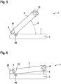
- Figs. 5 and 6 each show a schematic drawing of a sensor device 1 according to a second embodiment of the present invention.
- the detecting means 100 is not shown therein.
- Fig. 5 shows a state in which no molecule 20 is present or bound to the binding structure 5
- Fig. 6 shows a state in which a molecule 20 is bound to the binding structure 5.
- the sensor device 1 of the present embodiment includes the first structure 2, the second structure 3 and a hinge joint 4 as the joining portion 4.
- the hinge joint 4 is configured to allow a relative rotation of the first structure 2 to the second structure 3 (or vice versa) only around the first axis of rotation 6.
- the first axis of rotation 6 coincides with the location of the hinge joint 4.
- the binding structure 5 is disposed on the end face 12 of the first structure 2. Thereby, when a molecule 20, as shown in Fig. 6 , attaches and binds to the binding structure 5, the relative mobility around the first axis of rotation 6 is limited. The range of possible elevation angles 8 is thus reduced. This change in mobility can then be detected by the detecting means 100.
- the first structure 2 and the second structure 3 may both be plate-shaped or rod-like.
- the sensor device 1 of the present embodiment may comprise a rod-like second structure 3.
- any number of sensing mechanisms 2, 3, 4 and/or their constituent elements and/or detecting means 100 may be provided, as elucidated above.
- multiple or many first structures 2 may be provided on a single second structure 3.
- Figs. 7 , 8 and 9 each show a schematic drawing of a sensor device 1 according to a third embodiment of the present invention.
- the detecting means 100 is not shown therein.
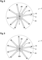
- Fig. 7 shows a general structure of the sensor device 1.
- Fig. 8 shows a state in which no molecule 20 is present or bound with/to the binding structure 5, whereas Fig. 9 shows a state in which a molecule 20 is bound with/to the binding structure 5.
- Figs. 8 and 9 show a top view of the sensor device 1.
- the sensor device 1 of the present embodiment includes the first structure 2 as a rod-like structure and the second structure 3 as a plate-shaped structure. Further, the joining portion 4 rotatably connects the first structure 2 and the second structure 3.
- the first structure 2, the second structure 3 and the joining portion 4 of the present embodiment are constructed similar to a hand of a clock (see also Figs. 8 and 9 ).
- the second axis of rotation 9 is perpendicular to the surface 7 of the second structure 3.
- the relative mobility of the first structure 2 to the second structure 3 (or vice versa) is only around the second axis of rotation 9.
- the joining portion 4 of the present embodiment does not allow a (substantial, destruction-free) rotation around the first axis of rotation 6.
- the binding structure 5 is disposed on the surface 7 of the second structure 3.
- Figs. 8 and 9 a range of mobility of one first structure 2 around the second axis of rotation 9 is shown. Therein, the possible pivot angle 10 of the first structure 2 is limited when the molecule 20 binds with/to the binding structure 5.
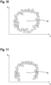
- Examples of measurement results detected by the detecting means 100 are shown in Figs. 10 and 11 .
- Fig. 10 shows an illustrative example of a measurement result obtained by the sensor device 1 shown in Fig. 8 , i.e. without molecule 20 being bound
- Fig. 11 shows an illustrative example of a measurement result obtained by the sensor device 1 shown in Fig. 9 , i.e. with a molecule 20 being bound.
- the detecting means 100 is configured to detect the change in relative mobility from the fluorescence signal emitted by the markers 13.
- the first structure 2 can rotate freely around the second axis of rotation 9.
- the first structure 2 is limited to a predetermined pivot angle 10 by the molecule 20.
- the sensor device 1 of the present embodiment may comprise a rod-like second structure 3.
- any number of sensing mechanisms 2, 3, 4 and/or their constituent elements and/or detecting means 100 may be provided, as elucidated above.
- multiple or many first structures 2 may be provided on a single second structure 3.
- Figs. 12 and 13 each show a schematic drawing of a sensor device 1 according to a fourth embodiment of the present invention.
- Fig. 14 shows an illustrative example of a measurement result obtained by the sensor device 1 shown in Figs. 12 and 13 .
- the general configuration of the first structure 2, the second structure 3 and the joining portion 4 of the present embodiment is similar to that of the second embodiment shown in Figs. 5 and 6 .
- the first structure 2 and the second structure 3 each comprise at least one fluorophore 23.
- the fluorophores 23 are configured to transfer energy between one another via FRET (Förster resonance energy transfer).
- FRET Förster resonance energy transfer
- the fluorophore(s) 23 attached to the first structure 2 may be (a) donor(s)
- the fluorophore(s) 23 attached to the second structure 3 may be (an) acceptor(s).
- the detecting means 100 is configured to detect changes in the fluorescence emitted by the fluorophores 23 and thereby detect changes in the relative mobility between the first structure 2 and the second structure 3 (and vice versa).
- Fig. 14 shows an illustrative measurement result thereof.
- the ordinate 21 is time and the abscissa 22 is the FRET signal detected by the detecting means 100.
- the FRET signal strongly increases. This indicates that a molecule 20 has been bound with/to the binding structure 5, thereby decreasing the mean or average distance between the first structure 2 and the second structure 3 and increasing the energy transfer via FRET.
- Figs. 15 and 16 each show a schematic drawing of a sensor device 1 according to a fifth embodiment of the present invention.
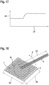
- Fig. 17 shows an illustrative example of a measurement result obtained by the sensor device 1 shown in Figs. 15 and 16 .
- the general configuration of the first structure 2, the second structure 3, and the joining portion 4 is similar to that of the first embodiment shown in Figs. 1 and 2 .
- the detection of relative mobility between the first structure 2 and the second structure 3 is based on surface plasmon resonance (SPR).
- a nanoparticle 19 is deposited on the distal end 18 of the first structure 2.
- the second structure 3 is disposed on a gold surface 24.
- the second structure 3 may be macrosized and consist of or comprise gold.
- the second structure 3 may form the gold surface 24.
- one or more first structures 2 may be attached, each via one joining portion 4, to said second structure 3 as the gold surface 24.
- gold may be deposited on the second structure 3, for example via sputtering, especially on a bottom surface (opposite the first structure 2) thereof.
- the detecting means 100 comprises a light source 101 and a detector 102.
- the light source 101 is configured to emit measurement light.
- the detector 102 is configured to measure light emitted by the light source 101 and reflected by the gold surface 24. Further, the detector 102 is configured to detect a surface plasmon resonance angle 25 of absorbed light due to surface plasmon resonance in the gold surface 24.
- the binding of the molecule 20 with/to the binding structure 5 limits the (mean or average) distance between the first structure 2 and the second structure 3, and thereby limits the distance between the nanoparticle 19 and the gold surface 24. This changes the surface plasmon resonance angle 25 and is detectable by the detector 102 of the detecting means 100.
- Fig. 17 shows an illustrative example of such a measurement result.
- the abscissa 21 is time and the ordinate 22 is a measurement signal readout by the detecting means 100.
- the measurement signal is anti-proportional to the mean or average distance between the nanoparticle 19 and the gold surface 24 (i.e. the surface plasmon resonance angle 25).
- the signal changes over time, thereby indicating a presence of molecule(s) 20.
- the foregoing described means of detection of the present embodiment may be combined with the other foregoing described configurations of the sensor device 1 and/or the other foregoing described means of detection (for example, simultaneous detection of FRET and SPR).
- Fig. 18 shows a schematic drawing of a sensor device 1 according to a sixth embodiment of the present invention.
- Fig. 18 shows an example of the sensor device 1 being formed of DNA origami structures.
- the second structure 3 is preferably a plate made of DNA structures comprising a length 16 and a width 26 of roughly 55 nm, respectively. Further, the length 14 of such a first structure 2 comprising DNA is roughly 400 nm. In one example, the length 14 is 436 nm.
- first structure 2, the second structure 3 and the joining portion 4 may be formed integrally with one another.
- the joining portion 4 may comprise a single strand of DNA or RNA connected to or being a part of (one rung thereof) the first structure 2 and the second structure 3.
- Any of the foregoing described embodiments may be formed of such DNA origami structures shown in Fig. 18 .
Landscapes
- Health & Medical Sciences (AREA)
- Physics & Mathematics (AREA)
- Immunology (AREA)
- Chemical & Material Sciences (AREA)
- General Health & Medical Sciences (AREA)
- Biochemistry (AREA)
- Analytical Chemistry (AREA)
- General Physics & Mathematics (AREA)
- Life Sciences & Earth Sciences (AREA)
- Pathology (AREA)
- Nuclear Medicine, Radiotherapy & Molecular Imaging (AREA)
- Chemical Kinetics & Catalysis (AREA)
- Optics & Photonics (AREA)
- Investigating Or Analyzing Materials By The Use Of Electric Means (AREA)
Abstract
The invention concerns a sensor device (1) for detecting the presence of one or more molecules (20) and/or of a class of molecules (20); comprising at least one first (nano-) structure (2); at least one second structure (3); at least one joining portion (4) respectively connecting the at least one first (nano-)structure (2) and the at least one second structure (3) and configured to allow a relative mobility between the at least one first (nano-)structure (2) and the at least one second structure (3), wherein the at least one joining portion (4) is an element separate from and connected to the at least one first (nano-)structure (2) and the at least one second structure (3) or wherein the at least one joining portion (4) is formed integrally with the at least one first (nano-)structure (2) and/or with the at least one second structure (3); one binding structure (5), especially one binding structure (5) per joining portion (4), configured to bind with a molecule, the presence of which is to be detected, wherein the binding structure (5) is located on the at least one first (nano-)structure (2) or on the at least one second structure (3) or on the at least one joining portion (4) such that said allowed relative mobility between the at least one first (nano-)structure (2) and the at least one second structure (3) is changed, especially limited, in a bound state of the binding structure (5) as compared to an unbound state of the binding structure (5); and a detecting means (100) for detecting said relative mobility between the at least one first (nano-)structure (2) and the at least one second structure (3).
Description
- The invention concerns a sensor device for detecting the presence of one or more molecules and/or for detecting the presence of a class of molecules.
- Conventionally, nanosensor systems for the detection of biomolecules such as cytokines are known from for example
US 2022/0183562 A1 . Such nanosensors as shown therein are commonly based on a tweezer principle, in which a binding of molecules causes a closing of a hinge of the tweezers, which in turn increases a photoacoustic signal provided by such tweezers. The photoacoustic signal is detected by detecting means. Furthermore, similar sandwich configurations of such nanosensors are known from for exampleUS 2022/0195421 A1 . In both cases, two arms of the tweezers or sandwich each include at least one binding molecule or receptor. When the molecule to be detected (for instance in the case ofUS 2022/0183562 A1 : cytokines) binds to the receptors on both arms, the signal provided by the nanosensor is changed such that the presence of the molecule can be detected. - These common solutions have the following disadvantages. Firstly, the detection of the molecule is only possible if the molecule binds to the binding molecules or receptors on both arms. Therefore, the sensitivity of such a sensor is rather low. Secondly, the molecule to be detected needs to be suitably large and needs to comprise at least two sections, especially two epitopes, which can bind to the multiple receptors. Therefore, the sensor is not suitable for the detection of smaller molecules or of molecules comprising only one binding section or epitope.
- It is an object of the present invention to overcome the foregoing described disadvantages of the prior art. In particular, it is an object of the present invention to provide a sensor device with a high sensitivity and which is capable of detecting a larger variety of molecules, especially smaller molecules.
- The solution of this object is achieved by the features of the independent claim. The dependent claims contain advantageous embodiments of the present invention.
- In particular, this object is solved by a sensor device for detecting the presence of one or more molecules and/or of a class of molecules comprising at least one first (nano-)structure, at least one second structure, at least one joining portion, one binding structure, especially one binding structure per joining portion, and a detecting means. Therein, the at least one joining portion respectively connects the at least one first (nano-)structure and the at least one second structure. The at least one joining portion is respectively configured to allow a relative mobility between the at least one first (nano-)structure and the at least one second structure. The at least one joining portion is an element separate from and connected to the at least one first (nano-)structure and the at least one second structure or is formed integrally with the at least one first (nano-)structure and/or with the at least one second structure. Furthermore, the one binding structure, especially the one binding structure per joining portion, is configured to bind with a molecule, the presence of which is to be detected. The binding structure is located on the at least one first (nano-)structure or on the at least one second structure or on the at least one joining portion such that said allowed relative mobility between the at least one first (nano-)structure and the at least one second structure is changed, especially limited, in a bound state of the binding structure as compared to an unbound state of the binding structure. Furthermore, the detecting means is configured to detect said relative mobility between the at least one first (nano-)structure and the at least one second structure.
- Thereby, especially since exactly one binding structure is provided per joining portion, the relative mobility is changed once the molecule to be detected binds to said exactly one binding structure. This change in relative mobility is detected by the detecting means. Therefore, the sensitivity of detection is high and smaller molecules can be detected by the sensor device according to the present invention.
- Herein, "relative mobility" refers to a destruction-free mobility. A "restriction of mobility" is to be understood as within the bounds of destruction-free movement.
- Preferably, the detecting means is configured to detect the relative mobility between the at least one first (nano-)structure and the at least one second structure before and after binding of the molecule(s) to be detected. Preferably, the detecting means is configured to detect a change in the relative mobility between before and after binding of the molecule(s) to be detected. Preferably, the detecting means is configured to detect a time-dependent signal, wherein a value, especially an intensity, of the signal is dependent on a relative mobility and thereby dependent on the binding state of the molecule(s) to be detected. Therefore, by detecting a (especially time-dependent) relative mobility between the respective first (nano-)structure and the second structure, the detecting means is configured to detect the presence of the molecule(s) to be detected.
- Preferably, each joining portion connects exactly one pair of the at least one first (nano-) structure and the at least one second structure. For instance, in the case of one first (nano-)structure and one second structure, one joining portion is provided connecting the two structures. In the case of equally multiple (for instance, five) first (nano-)structures and multiple (correspondingly also five) second structures, an equal multiple (correspondingly also five) of joining portions is provided connecting each first (nano-)structure to one second structure. Further for instance, in case exactly one second structure and multiple first (nano-) structures (or vice versa) are provided, the number of joining portions corresponds to the number of the multiple first (nano-)structures (or vice versa).
- Advantageously, the at least one first (nano-)structure is a nanostructure.
- Preferably, the at least one second structure is a nanostructure.
- Preferably, the at least one joining portion is a nanostructure.
- Herein, unless certain dimensions are further specified, the term "nanosized" or "nanostructure" refers to the respectively referred to element or object having a size in at least one of its dimensions (length, width, height) of at least one or a few to a few tens of nanometers (for example 10 nm to 50 nm), especially less than 1000 nm (less than 1 µm). Preferably, not all dimensions of said element or object are necessarily "nanosized". For example, a length of one element or object may be equal to or higher than 1000 nm, this element or object nonetheless being referred to as "nanosized" or "nanostructure" due to preferably a width or height thereof being only a few to a few tens or a few hundreds of nanometers. Most preferably, no more than one dimension (length, width, height) of the respective object or element as a nanostructure is equal to or higher than 1000 nm. In other words, preferably, at least two of its dimensions (length, width, height) are of at least one or a few to a few tens of nanometers (for example 10 nm to 50 nm), especially less than 1000 nm (less than 1 µm).
- Preferably, the nanostructured element or object, especially the at least one first (nano-) structure, is formed at least partially or entirely of a DNA origami structure.
- In one advantageous embodiment, the at least one first (nano-)structure is a rod-like structure. In addition or alternatively, the at least one second structure is preferably a plate-shaped structure.
- Herein, the term "rod-like structure" preferably refers to an object with a length significantly greater than its width and/or height. For example, a length of such rod-like structure as a nanostructure may be few tens to few hundreds nm, for example roughly 300 nm to 500 nm, particularly roughly 400 nm, whereas a width and height thereof may respectively be a few nm, for example 5 nm to 10 nm, thereby preferably constituting a rod shape.
- Further herein, the term "plate-shaped structure" preferably refers to an object with a length and width significantly greater than its height. Herein, preferably, length and width thereof are not necessarily equal. For example, a length and width of such plate-shaped structure as a nanostructure may be few tens to few hundreds nm, for example 30 nm to 60 nm, whereas a height thereof may be a few nm, for example 2 nm to 10 nm.
- Preferably, the plate-shaped structure refers to a flat plate-shaped structure, with at least one, especially all, surface(s) thereof being substantially flat.
- In some embodiments, the at least one first (nano-)structure and the at least one second structure are both rod-like structures. Preferably, the at least one first rod-like (nano-) structure and the at least one second rod-like structure are connected via one joining portion.
- In some embodiments, the at least one first (nano-)structure and the at least one second structure are both plate-shaped structures. Preferably, the at least one first plate-shaped (nano-)structure and the at least one second plate-shaped structure are connected via one joining portion.
- Preferably, at least one first (nano-)structure is a rod-like structure and at least one second structure is a plate-shaped structure or vice versa. Preferably therein, at least two, especially many, rod-like first (nano-)structures are connected to one plate-shaped second structure, preferably each via one joining portion.
- In a further advantageous embodiment, the sensor device preferably comprises exactly one second structure. Preferably therein, the exactly one second structure is a macrostructure, wherein "macrostructure" describes at least one dimension (length, width, height) being preferably larger than aforementioned nanostructure or nanosized dimension. For example, in a macrostructure, preferably at least two dimensions may be 1 µm or more, preferably 10 µm or more, more preferably 100 µm or more. Therein, for example, the exactly one second structure is preferably a macrosized plate-shaped structure. For example, the exactly one second structure is preferably a plate with a length and a width of a few hundred µm to a few mm, respectively. At least two, especially many, first (nano-)structures may be attached via respective joining portions to such a macrosized plate-shaped structure as the exactly one second structure.
- Preferably, the at least one joining portion is configured to allow a relative rotation as said relative mobility of the at least one first (nano-)structure relative to the at least one second structure.
- In one advantageous embodiment, a first axis of rotation is parallel to a plane defined by an extension of a surface of the at least one second structure with which the at least one joining portion is formed integrally or to which the at least one joining portion is connected. Therein, the binding structure is configured to - in the bound state - limit said allowed relative rotation around the first axis of rotation to a predefined elevation angle.
- Preferably therein, the at least one joining portion allows the first (nano-)structure to rotate to a predetermined elevation angle - in the unbound state - of 0° to 180°, preferably of 20° to 160°, more preferably of 45° to 135° and most preferably of between 0° and 90° or of between 0° and 45°. Preferably, in the bound state, the allowed relative rotation around the first axis of rotation is limited to a relative rotation of roughly half of the allowed relative rotation in the unbound state. Preferably, the relative rotation in the bound state of the binding structure is limited by between more than 0° and equal to or less than 90°, more preferably by between more than 0° and equal to or less than 45°, most preferably by between more than 0° and equal to or less than 30°. Herein, "limited by between X° and Y°" preferably means limiting, in the bound state, the rotatable range of the unbound state by a value between minimum X° and maximum Y° of limitation of the rotatable range (a change or delta of allowable rotation angles). For example, in the preferable case of the joining portion allowing a rotation of 0° to 180° in the unbound state, if limited by between more than 0° and equal to or less than 90° in the bound state, the relative rotation may be limited by a value up to 90°. In the case of limitation by 90°, a rotation in the bound state is allowed between relative positions 0° and 90° or between 90° and 180° or between
relative positions 20° and 110°, for example (180° - 90° = 90°). Further therein, for example, limitation thereof by 70° (being within the range of more than 0° and less than 90°) can allow a relative rotation by between 0° and 110° (180° - 70° = 110°), etc. - Preferably, a second axis of rotation is perpendicular to a plane defined by an extension of a surface of the at least one second structure with which the at least one joining portion is formed integrally or to which the at least one joining portion is connected. The binding structure is configured to - in the bound state - limit said allowed relative rotation around the second axis of rotation to a predefined pivot angle.
- Preferably, the second axis of rotation is perpendicular to the first axis of rotation.
- Preferably, the joining portion is configured to allow a relative rotation of the at least one first (nano-)structure relative to the second structure around both the first axis of rotation and the second axis of rotation.
- Advantageously, the joining portion is configured to allow a relative rotation of the at least one first (nano-)structure relative to the second structure only around the first axis of rotation or only around the second axis of rotation.
- In one advantageous embodiment, the at least one joining portion is a hinge joint. Preferably, such hinge joint is configured to restrict a rotation to one axis of rotation, especially to the first axis of rotation. Thereby, the relative mobility is restricted to one axis of rotation, which simplifies the detection thereof.
- Preferably, the binding structure is located on an end section, especially on an end face, of the at least one first (nano-)structure adjacent to the at least one joining portion. Thereby, the molecule to be detected is preferably bound to the respective first (nano-)structure such that a relative mobility of the first (nano-)structure is restricted by said bound molecule. Therein, the bound molecule is preferably disposed between the end section, especially the end face, of the first (nano-)structure and the respective second structure, such that the relative mobility of the first (nano-)structure is limited.
- Alternatively, the binding structure is located on a surface of the at least one second structure. Therein, the binding structure is located on the surface of the at least one second structure so as to hinder a relative rotation of the at least one first (nano-)structure, especially around the second axis of rotation. Advantageously, the binding structure is located on the surface of the at least one second structure adjacent to the at least one joining portion. Thereby, the molecule to be detected is preferably bound to the respective second structure such that a relative mobility of the first (nano-)structure is restricted by said bound molecule. In both aforementioned cases of the binding structure being located preferably on an end section of the at least one first (nano-)structure or on a surface of the at least one second structure, the bound molecule is wedged between the at least one first (nano-)structure and the at least one second structure near the joining portion, such that said relative mobility between the at least first (nano-)structure and the at least one second structure is limited by the bound molecule.
- Advantageously, the binding structure is located on or at an interface of at least two out of the at least one first (nano-)structure, the at least one second structure, and the at least one joining portion. For example, the binding structure may be located on or at an interface between the at least one first (nano-)structure and the at least one joining portion. Alternatively, in a preferable embodiment, the binding structure is located only on the at least one first (nano-)structure or only on the at least one second structure or only on the at least one joining portion.
- In one advantageous embodiment, at least two of the at least one first structure, the at least one second structure, and the at least one joining portion are formed integrally with one another, especially as a continuous (nano-)structure. For example, one first (nano-)structure and one second structure are preferably formed as a single continuous (nano-)structure. Further for example, one first structure and one joining portion are preferably formed as a single continuous (nano-)structure. Further for example, one joining portion and one second structure are formed as a single continuous (nano-)structure. The aforementioned continuous (nano-)structure is further connected to the other remaining structure or joining portion, which is not a part of the continuous (nano-)structure. The continuous nano-structure may preferably be combined with or attached to further macro-structures. For example, one first (nano-)structure and one joining portion may be formed as a single continuous (nano-) structure and may be further attached to a macrosized second structure such as a macrosized plate.
- Preferably, all of the at least one first (nano-)structure, the at least one second structure, and the at least one joining portion are formed integrally, especially as a continuous (nano-) structure.
- Advantageously, the binding structure is configured to bind with a predetermined organic molecule, especially with a predetermined bio-molecule. For example, the binding structure is preferably configured to bind with DNA and/or RNA and/or ssDNA (single-stranded DNA) and/or ssRNA (single-stranded RNA) and/or proteins and/or small molecules and/or antibodies.
- In one advantageous embodiment, each binding structure is configured to bind with exactly one molecule. In a further advantageous embodiment, at least one or each binding structure is configured to bind with more than one molecule. For example, at least one or each binding structure may comprise multiple receptors, each for one molecule, especially for exactly one molecule. Preferably therein, multiple receptors (for instance two) of one such binding structure are not configured to bind to a single molecule in common. Therein, preferably, such binding structure(s) is/are configured to limit the relative mobility (in a bound state), especially in dependence on the number of bound binding structures.
- Preferably, the binding structure comprises or consists of ssDNA and/or aptamers and/or nanobodies and/or antibodies and/or proteins and/or small molecules. One example of nanobodies is a fragment of an antibody. Another example is a single-domain antibody, especially a camelid nanobody from for example a llama or the like.
- Preferably, the binding structure comprises or consists of ssDNA, wherein the molecule to be detected is ssDNA and/or ssRNA.
- Preferably, the binding structure comprises or consists of aptamers, wherein the molecule to be detected is preferably one or more proteins. More preferably therein, the molecule to be detected is a small molecule.
- Further preferably, the binding structure comprises or consists of one or more nanobodies, wherein the molecule to be detected is most preferably one or more proteins. Alternatively or in addition thereto, the molecule to be detected is one or more antibodies.
- Further preferably, the binding structure comprises or consists of one or more antibodies, wherein the molecule to be detected is most preferably one or more proteins.
- Further preferably, the binding structure comprises or consists of one or more proteins, wherein the molecule to be detected is most preferably one or more antibodies.
- Further preferably, the binding structure comprises or consists of one or more small molecules, wherein the molecule to be detected is most preferably one or more antibodies.
- In one advantageous embodiment, at least one of the at least one first (nano-)structure, the at least one second structure, and the at least one joining portion comprises or consists of a nucleic acid structure and/or a protein. DNA and RNA are preferable examples of such nucleic acid structures.
- Preferably, at least two of the at least one first (nano-)structure, the at least one second structure, and the at least one joining portion comprise or consist of DNA or RNA. Preferably therein, the number of strands (single stranded or double stranded) varies between them. For example, the at least one first (nano-)structure may comprise double stranded DNA, the joining portion may comprise single stranded DNA, and the second structure may comprise double stranded DNA.
- In one advantageous embodiment, the at least one first (nano-)structure and/or the at least one second structure comprise(s) a marker, especially a fluorescence marker. Preferably, the detecting means is a microscope, in particular preferably a fluorescence microscope. The detecting means is preferably configured to detect a movement of said marker. Preferably, the detecting means is configured to detect a (continuous) time-dependent movement of said marker (i.e. a movement over time or time-resolved), which indicates the relative mobility. By detecting a time-dependent movement of the marker, the detecting means is preferably configured to thereby detect the relative mobility of the at least one first (nano-)structure relative to the at least one second structure depending on a binding state of the molecule(s) to be detected. Preferably therein, the detecting means is configured to detect only a time-dependent movement of said marker(s), especially without detecting or computing absolute intensities or their changes.
- Preferably, in a case in which the at least second structure is plate-shaped, and the at least one first (nano-)structure is rod-like, the joining portion being disposed at one end of the rod-like first (nano-)structure and attaching said first (nano-)structure to a surface of the second structure, the one or more markers, especially fluorescence marker(s), is/are disposed at a distal end of the first (nano-)structure opposite the end to which the joining portion is attached.
- Preferably, the at least one first (nano-)structure and the at least one second structure each comprise at least one fluorophore. Therein, the detecting means is configured to detect a Förster Resonance Energy Transfer (FRET) between said fluorophores comprised by the at least one first (nano-)structure and the at least one second structure. Preferably, the amount of FRET, i.e. the amount of energy transferred between the fluorophores, is dependent on the relative mobility between the respective first (nano-)structure and second structure. For example, with higher mobility, i.e. in an unbound state of the molecule(s) to be detected, FRET may be lower than with lower mobility, i.e. in a bound state of the molecule(s) to be detected. Especially by detecting a time-dependent FRET, especially a time-dependent FRET intensity signal, the detecting means is thereby configured to detect the relative mobility between the respective first (nano-)structure and the second structure and to thereby detect the presence of the molecule(s) to be detected.
- Further preferably, the detecting means is configured to detect a surface plasmon resonance (SPR) between the at least one first (nano-)structure and the at least one second structure. Preferably, the SPR signal is time-dependent, wherein the signal, especially its intensity, changes depending on the relative mobility of the respective first (nano-)structure and the second structure. For instance, the SPR signal intensity increases with lower relative mobility, such that the SPR signal increases in intensity under presence of the molecule(s) to be detected.
- Preferably, at least one of the at least one first (nano-)structure and the at least one second structure comprise(s) a nanoparticle, preferably a gold nanoparticle. Preferably, the nanoparticle is disposed at a distal end of the respective first (nano-)structure, especially opposite the joining portion. Thereby, sensitivity to SPR is advantageously increased.
- Further details, advantages, and features of the preferred embodiments of the present invention are described in detail with reference to the figures. Therein:
-
Fig. 1 shows a schematic drawing of a sensor device according to a first embodiment of the present invention; -
Fig. 2 shows a schematic drawing of the sensor device according to the first embodiment of the present invention; -
Fig. 3 shows an illustrative example of a measurement result obtained by the sensor device shown inFig. 1 ; -
Fig. 4 shows an illustrative example of a measurement result obtained by the sensor device shown inFig. 2 ; -
Fig. 5 shows a schematic drawing of a sensor device according to a second embodiment of the present invention; -
Fig. 6 shows a schematic drawing of the sensor device according to the second embodiment of the present invention; -
Fig. 7 shows a schematic drawing of a sensor device according to a third embodiment of the present invention; -
Fig. 8 shows a schematic drawing of the sensor device according to the third embodiment of the present invention; -
Fig. 9 shows a schematic drawing of the sensor device according to the third embodiment of the present invention; -
Fig. 10 shows an illustrative example of a measurement result obtained by the sensor device shown inFig. 8 ; -
Fig. 11 shows an illustrative example of a measurement result obtained by the sensor device shown inFig. 9 ; -
Fig. 12 shows a schematic drawing of a sensor device according to a fourth embodiment of the present invention; -
Fig. 13 shows a schematic drawing of the sensor device according to the fourth embodiment of the present invention; -
Fig. 14 shows an illustrative example of a measurement result obtained by the sensor device shown inFigs. 12 and 13 ; -
Fig. 15 shows a schematic drawing of a sensor device according to a fifth embodiment of the present invention; -
Fig. 16 shows a schematic drawing of the sensor device according to the fifth embodiment of the present invention; -
Fig. 17 shows an illustrative example of a measurement result obtained by the sensor device shown inFigs. 15 and 16 ; and -
Fig. 18 shows a schematic drawing of a sensor device according to a sixth embodiment of the present invention. -
Figs. 1 and 2 each show a schematic drawing of asensor device 1 according to a first embodiment of the present invention. - In particular, as will be explained in more detail below,
Fig. 1 shows thesensor device 1 when nomolecule 20, the presence of which is to be detected by thesensor device 1, is present. -
Fig. 2 shows thesensor device 1 when saidmolecule 20 is present in or near thesensor device 1. - As stated, the
sensor device 1 is configured to detect the presence of one ormore molecules 20 and/or a class ofmolecules 20. - The
sensor device 1 of the present embodiment comprises onefirst structure 2 and onesecond structure 3. Herein, thefirst structure 2 is a rod-like structure. Thesecond structure 3 is a plate-shaped structure. - In particular, in the present embodiment, the
first structure 2 and thesecond structure 3 are each nanosized. In the present embodiment, thefirst structure 2 and thesecond structure 3 are each entirely nanosized. In other words, all of their respective dimensions (length, width, height) are less than 1000 nm. For example, alength 14 of thefirst structure 2 is 100 nm to 500 nm, especially roughly 400 nm, preferably 436 nm. For example, awidth 15 of thefirst structure 2 is 3 nm to 10 nm, preferably roughly 7 nm. For example a height (in depth direction ofFig. 1 ) of thefirst structure 2 is preferably 3 nm to 10 nm, preferably roughly 7 nm. Preferably, thewidth 15 and the height of thefirst structure 2 are equal. For example, alength 16 of thesecond structure 3 is 40 nm to 100 nm, preferably roughly 55 nm. For example, a width (in depth direction ofFig. 1 ) of thesecond structure 3 is 40 nm to 100 nm, preferably roughly 55 nm. Preferably,length 16 and width of thesecond structure 3 are equal. For example, aheight 17 of thesecond structure 3 is 3 nm to 10 nm, preferably roughly 7 nm. Preferably, aheight 17 of thesecond structure 3 is equal to thewidth 15 and/or a height of thefirst structure 2. - The
sensor device 1 further comprises a joiningportion 4. The joiningportion 4 connects thefirst structure 2 to thesecond structure 3. In the present embodiment, the joiningportion 4 is an element separate from thefirst structure 2 and thesecond structure 3. In other words, the joiningportion 4 of the present embodiment is not formed integrally with thefirst structure 2 or with thesecond structure 3. - The joining
portion 4 is configured to serve as a joint connecting thefirst structure 2 and thesecond structure 3. The joiningportion 4 is configured to allow a relative mobility between thefirst structure 2 and thesecond structure 3. - In the present embodiment, the relative mobility is an allowed rotation of the
first structure 2 relative to the second structure 3 (or vice versa). Herein, one first axis ofrotation 6 is parallel to a plane defined by an extension of asurface 7 of thesecond structure 3. As can be taken fromFigs. 1 and 2 , the axis ofrotation 6 extends in a depth direction, especially perpendicular to a substantial extension of thefirst structure 2. - Furthermore, an
elevation angle 8 is defined between thefirst structure 2 and thesecond structure 3. In particular, theelevation angle 8 is defined between thesurface 7 of thesecond structure 3 and thefirst structure 2. - In the present embodiment, as will be explained with respect to
Figs. 3 and 4 , the relative mobility of thefirst structure 2 relative to thesecond structure 3 is not limited to the aforementioned first axis ofrotation 6, i.e. to theelevation angle 8. Herein, the first structure 2 (or the second structure 3) is also allowed to rotate around a second axis ofrotation 9 around a pivot angle 10 (not shown). Thispivot angle 10 will be described in more detail in view ofFigs. 7 to 11 . The second axis ofrotation 9 is perpendicular to the plane defined by the extension of thesurface 7 of thesecond structure 3. - The
sensor device 1 further comprises abinding structure 5. Thebinding structure 5 is configured to bind with themolecule 20, th e presence of which is to be detected. For example, the bindingstructure 5 is single stranded DNA or RNA (ssDNA, ssRNA), which is configured to bind to further ssDNA or ssRNA. - The
binding structure 5 is located on an end section, particularly on anend face 12 of thefirst structure 2. - When a
molecule 20 binds with/to thebinding structure 5, the relative mobility between thefirst structure 2 and thesecond structure 3 is changed, especially limited. In the present embodiment, as a comparison ofFig. 1 withFig. 2 shows, theelevation angle 8 is limited once themolecule 20 binds with or to thebinding structure 5. Preferably, themolecule 20 binds with/to thebinding structure 5 and mechanically blocks the relative rotation of thefirst structure 2 to the second structure 3 (or vice versa) around the first axis ofrotation 6. - Thereby, the presence of molecule(s) 20 has the effect of changing or limiting the relative mobility between the
first structure 2 and thesecond structure 3. - The
sensor device 1 further comprises a detecting means 100 which is configured to detect the relative mobility between thefirst structure 2 and thesecond structure 3. - In the present embodiment, the
first structure 2 comprises at least one, especially a plurality of,markers 13. Herein, themarkers 13 are fluorescence markers. Themarkers 13 are disposed near adistal end 18 of thefirst structure 2 opposite theend face 12. In particular, themarkers 13 are disposed within a distal end portion extending roughly 10 % of theoverall length 14 of the first structure 2 (i.e. arranged within distal 10 % of the first structure 2). - The detecting means 100 is especially a fluorescence microscope configured to detect a fluorescence signal emitted by the
markers 13. Furthermore, the detecting means 100 is configured to detect said signal over a predetermined period of time. Thereby, the detecting means 100 is configured to detect positions of themarkers 13 over time. When the relative mobility of thefirst structure 2, which comprises themarkers 13, is changed or limited by the binding of themolecule 20 with/to thebinding structure 5, the detecting means 100 detects a changed signal. - Examples of such signals are shown in
Figs. 3 and 4 . Therein,Fig. 3 shows an illustrative example of a measurement result obtained by thesensor device 1 shown inFig. 1 , whereasFig. 4 shows an illustrative example of a measurement result obtained by thesensor device 1 shown inFig. 2 . In other words,Fig. 3 shows a measurement result before (or without) binding of themolecule 20 with/to thebinding structure 5, andFig. 4 shows a measurement result after (or with) binding of themolecule 20 with/to thebinding structure 5. - Therein, in each of
Figs. 3 and 4 , the fluorescence signals emitted by themarkers 13 are shown, wherein multiple measurement points are recorded over time and shown with respect to space dimensions X and Y. Herein, the space dimensions X and Y coincide with thelength 16 and the width of thesecond structure 3. In other words, as shown inFigs. 1 and 2 , the detecting means 100 views a top view onto thefirst structure 2 and thesecond structure 3. - As can be taken from
Fig. 3 , when nomolecule 20 is present or bound with/to thebinding structure 5, thefirst structure 2 can freely rotate around the first axis ofrotation 6 and the second axis ofrotation 9. Thereby, the measurement points theoretically (given sufficient time and measurements) span all points within a circle having a radius roughly equal to thelength 14 of thefirst structure 2. - Once the
molecule 20 binds with/to thebinding structure 5, as shown inFig. 2 , the relative rotation of thefirst structure 2 around the first axis ofrotation 6 is limited to a predetermined range of elevation angles 8. Thereby, the measurement points describe a ring, due to further rotation around the second axis ofrotation 9 being possible. - Thus, by measuring the signal emitted by the
markers 13 overtime, the detecting means 100 is capable of detecting the relative mobility between thefirst structure 2 and thesecond structure 3 over time and is therefore capable of detecting a presence of the molecule(s) 20. - Preferably, the
first structure 2, thesecond structure 3 and the joiningportion 4 are each formed of a DNA origami structure. - In the following, for ease of explanation, the
first structure 2, thesecond structure 3 and the joiningportion 4 may in summary be denoted as "sensor mechanism sensor device 1 may also be described as comprising asensor mechanism means 100. - Although the foregoing described embodiment comprises one
first nanostructure 2, onesecond nanostructure 3 and one joiningportion 4, it should be noted that multiples of at least one or more, especially all, of the foregoingelements sensor device 1. - For example, the
sensor device 1 may comprisemultiple sensor mechanisms means 100. In one example, thesensor device 1 comprises many (i.e. in the order of hundreds)sensor mechanisms molecules 20 is to be detected. In such an example, the detecting means 100 is configured to detect the relative mobility between thefirst structure 2 and thesecond structure 3 of thesensing mechanisms sensing mechanisms sensing mechanisms molecules 20 are present, since thesensing mechanisms second structure 3 may be a rod-like structure. - In another example, one or more of the foregoing
elements second structure 3 is a plate-shaped macrostructure. Therein, thesecond structure 3 can comprise a length and/or width of at least 1 µm, preferably of multiple millimeters. On saidsecond macrostructure 3, a plurality (i.e. 2 to 10), especially many (i.e. in the order of hundreds) offirst structures 2 as nanostructures can be disposed and connected thereto, each by one joiningportion 4. Therein, one detecting means 100 may be provided capable of detecting the relative mobility of any one or more, especially of all, suchfirst structures 2. Alternatively, a plurality of detectingmeans 100 may be provided. -
Figs. 5 and 6 each show a schematic drawing of asensor device 1 according to a second embodiment of the present invention. For ease of explanation, the detecting means 100 is not shown therein.Fig. 5 shows a state in which nomolecule 20 is present or bound to thebinding structure 5, whereasFig. 6 shows a state in which amolecule 20 is bound to thebinding structure 5. - The
sensor device 1 of the present embodiment includes thefirst structure 2, thesecond structure 3 and a hinge joint 4 as the joiningportion 4. - Therein, the
hinge joint 4 is configured to allow a relative rotation of thefirst structure 2 to the second structure 3 (or vice versa) only around the first axis ofrotation 6. Herein, the first axis ofrotation 6 coincides with the location of thehinge joint 4. - Similar to the first embodiment, the binding
structure 5 is disposed on theend face 12 of thefirst structure 2. Thereby, when amolecule 20, as shown inFig. 6 , attaches and binds to thebinding structure 5, the relative mobility around the first axis ofrotation 6 is limited. The range of possible elevation angles 8 is thus reduced. This change in mobility can then be detected by the detectingmeans 100. - Preferably, the
first structure 2 and thesecond structure 3 may both be plate-shaped or rod-like. - As also described with respect to the first embodiment, the
sensor device 1 of the present embodiment may comprise a rod-likesecond structure 3. Further, any number ofsensing mechanisms means 100 may be provided, as elucidated above. For example, multiple or manyfirst structures 2 may be provided on a singlesecond structure 3. -
Figs. 7 ,8 and 9 each show a schematic drawing of asensor device 1 according to a third embodiment of the present invention. For ease of explanation, the detecting means 100 is not shown therein.Fig. 7 shows a general structure of thesensor device 1.Fig. 8 shows a state in which nomolecule 20 is present or bound with/to thebinding structure 5, whereasFig. 9 shows a state in which amolecule 20 is bound with/to thebinding structure 5. Further,Figs. 8 and 9 show a top view of thesensor device 1. - As can be taken from
Fig. 7 , thesensor device 1 of the present embodiment includes thefirst structure 2 as a rod-like structure and thesecond structure 3 as a plate-shaped structure. Further, the joiningportion 4 rotatably connects thefirst structure 2 and thesecond structure 3. Thefirst structure 2, thesecond structure 3 and the joiningportion 4 of the present embodiment are constructed similar to a hand of a clock (see alsoFigs. 8 and 9 ). The second axis ofrotation 9 is perpendicular to thesurface 7 of thesecond structure 3. Herein, the relative mobility of thefirst structure 2 to the second structure 3 (or vice versa) is only around the second axis ofrotation 9. The joiningportion 4 of the present embodiment does not allow a (substantial, destruction-free) rotation around the first axis ofrotation 6. - Furthermore, the binding
structure 5 is disposed on thesurface 7 of thesecond structure 3. - In
Figs. 8 and 9 , a range of mobility of onefirst structure 2 around the second axis ofrotation 9 is shown. Therein, thepossible pivot angle 10 of thefirst structure 2 is limited when themolecule 20 binds with/to thebinding structure 5. - Examples of measurement results detected by the detecting means 100 are shown in
Figs. 10 and 11 . -
Fig. 10 shows an illustrative example of a measurement result obtained by thesensor device 1 shown inFig. 8 , i.e. withoutmolecule 20 being bound, andFig. 11 shows an illustrative example of a measurement result obtained by thesensor device 1 shown inFig. 9 , i.e. with amolecule 20 being bound. - As can be taken therefrom, the detecting means 100 is configured to detect the change in relative mobility from the fluorescence signal emitted by the
markers 13. InFigs. 8 and10 , thefirst structure 2 can rotate freely around the second axis ofrotation 9. InFigs. 9 and11 , thefirst structure 2 is limited to apredetermined pivot angle 10 by themolecule 20. - Similar to the description of the first and second embodiments, the
sensor device 1 of the present embodiment may comprise a rod-likesecond structure 3. Further, any number ofsensing mechanisms means 100 may be provided, as elucidated above. For example, multiple or manyfirst structures 2 may be provided on a singlesecond structure 3. -
Figs. 12 and 13 each show a schematic drawing of asensor device 1 according to a fourth embodiment of the present invention.Fig. 14 shows an illustrative example of a measurement result obtained by thesensor device 1 shown inFigs. 12 and 13 . - The general configuration of the
first structure 2, thesecond structure 3 and the joiningportion 4 of the present embodiment is similar to that of the second embodiment shown inFigs. 5 and 6 . - Herein, however, the
first structure 2 and thesecond structure 3 each comprise at least onefluorophore 23. Therein, thefluorophores 23 are configured to transfer energy between one another via FRET (Förster resonance energy transfer). For example, the fluorophore(s) 23 attached to thefirst structure 2 may be (a) donor(s), and the fluorophore(s) 23 attached to thesecond structure 3 may be (an) acceptor(s). - Thereby, when a
molecule 20 binds with/to thebinding structure 5 and thereby limits the relative mobility with respect to theelevation angle 8, a (mean or average) distance between thefluorophores 23 of thefirst structure 2 and thesecond structure 3 decreases, thus increasing the amount of energy transferred via FRET. - The detecting means 100 is configured to detect changes in the fluorescence emitted by the
fluorophores 23 and thereby detect changes in the relative mobility between thefirst structure 2 and the second structure 3 (and vice versa). -
Fig. 14 shows an illustrative measurement result thereof. Therein, theordinate 21 is time and theabscissa 22 is the FRET signal detected by the detectingmeans 100. - As can be taken from
Fig. 14 , over time, the FRET signal strongly increases. This indicates that amolecule 20 has been bound with/to thebinding structure 5, thereby decreasing the mean or average distance between thefirst structure 2 and thesecond structure 3 and increasing the energy transfer via FRET. - The foregoing described detection via FRET can be combined with the other foregoing described embodiments.
-
Figs. 15 and 16 each show a schematic drawing of asensor device 1 according to a fifth embodiment of the present invention.Fig. 17 shows an illustrative example of a measurement result obtained by thesensor device 1 shown inFigs. 15 and 16 . - In the present embodiment, the general configuration of the
first structure 2, thesecond structure 3, and the joiningportion 4 is similar to that of the first embodiment shown inFigs. 1 and 2 . - Herein, however, the detection of relative mobility between the
first structure 2 and thesecond structure 3 is based on surface plasmon resonance (SPR). - In the present embodiment, a
nanoparticle 19 is deposited on thedistal end 18 of thefirst structure 2. - Further, the
second structure 3 is disposed on agold surface 24. Alternatively, thesecond structure 3 may be macrosized and consist of or comprise gold. In other words, thesecond structure 3 may form thegold surface 24. Therein, one or morefirst structures 2 may be attached, each via one joiningportion 4, to saidsecond structure 3 as thegold surface 24. Alternatively to thesecond structure 3 forming thegold surface 24, gold may be deposited on thesecond structure 3, for example via sputtering, especially on a bottom surface (opposite the first structure 2) thereof. - The detecting means 100 comprises a
light source 101 and adetector 102. Thelight source 101 is configured to emit measurement light. Thedetector 102 is configured to measure light emitted by thelight source 101 and reflected by thegold surface 24. Further, thedetector 102 is configured to detect a surfaceplasmon resonance angle 25 of absorbed light due to surface plasmon resonance in thegold surface 24. - Herein, the binding of the
molecule 20 with/to thebinding structure 5 limits the (mean or average) distance between thefirst structure 2 and thesecond structure 3, and thereby limits the distance between thenanoparticle 19 and thegold surface 24. This changes the surfaceplasmon resonance angle 25 and is detectable by thedetector 102 of the detectingmeans 100. -
Fig. 17 shows an illustrative example of such a measurement result. Therein, theabscissa 21 is time and theordinate 22 is a measurement signal readout by the detectingmeans 100. The measurement signal is anti-proportional to the mean or average distance between thenanoparticle 19 and the gold surface 24 (i.e. the surface plasmon resonance angle 25). As can be taken fromFig. 17 , the signal changes over time, thereby indicating a presence of molecule(s) 20. - The foregoing described means of detection of the present embodiment may be combined with the other foregoing described configurations of the
sensor device 1 and/or the other foregoing described means of detection (for example, simultaneous detection of FRET and SPR). -
Fig. 18 shows a schematic drawing of asensor device 1 according to a sixth embodiment of the present invention. - Herein, the general configuration of the
sensor device 1 is similar to the configuration of thesensor device 1 of the first embodiment shown inFigs. 1 and 2 . Herein,Fig. 18 shows an example of thesensor device 1 being formed of DNA origami structures. - Therein, the
second structure 3 is preferably a plate made of DNA structures comprising alength 16 and awidth 26 of roughly 55 nm, respectively. Further, thelength 14 of such afirst structure 2 comprising DNA is roughly 400 nm. In one example, thelength 14 is 436 nm. - Although a detailed structure of the
surface 7 of thesecond structure 3 due to the DNA structure is shown, this is further defined as a flat plate-shape. In other words, in relation to a height of thesecond structure 3, saidsecond structure 3 does not comprise substantial projections or recesses therein. - Further, although not shown, the
first structure 2, thesecond structure 3 and the joiningportion 4 may be formed integrally with one another. For example, the joiningportion 4 may comprise a single strand of DNA or RNA connected to or being a part of (one rung thereof) thefirst structure 2 and thesecond structure 3. - Any of the foregoing described embodiments may be formed of such DNA origami structures shown in
Fig. 18 . - In addition to the foregoing written explanations, it is explicitly referred to
figures 1 to 18 , which in detail show configuration examples of the invention. -
- 1
- sensor device
- 2
- first structure
- 3
- second structure
- 4
- joining portion
- 5
- binding structure
- 6
- first axis of rotation
- 7
- surface
- 8
- elevation angle
- 9
- second axis of rotation
- 10
- pivot angle
- 12
- end face
- 13
- marker
- 14
- length of first structure
- 15
- width of first structure
- 16
- length of second structure
- 17
- height of second structure
- 18
- distal end of first structure
- 19
- nanoparticle
- 20
- molecule
- 21
- abscissa
- 22
- ordinate
- 23
- fluorophore
- 24
- gold surface
- 25
- surface plasmon resonance angle
- 26
- width of second structure
- 100
- detecting means
- 101
- light source
- 102
- detector
Claims (15)
- Sensor device (1) for detecting the presence of one or more molecules (20) and/or of a class of molecules (20); comprising:at least one first (nano-)structure (2);at least one second structure (3);at least one joining portion (4) respectively connecting the at least one first (nano-) structure (2) and the at least one second structure (3) and configured to allow a relative mobility between the at least one first (nano-)structure (2) and the at least one second structure (3), wherein the at least one joining portion (4) is an element separate from and connected to the at least one first (nano-)structure (2) and the at least one second structure (3) or wherein the at least one joining portion (4) is formed integrally with the at least one first (nano-)structure (2) and/or with the at least one second structure (3);one binding structure (5), especially one binding structure (5) per joining portion (4), configured to bind with a molecule, the presence of which is to be detected, whereinthe binding structure (5) is located on the at least one first (nano-)structure (2) or on the at least one second structure (3) or on the at least one joining portion (4) such that said allowed relative mobility between the at least one first (nano-)structure (2) and the at least one second structure (3) is changed, especially limited, in a bound state of the binding structure (5) as compared to an unbound state of the binding structure (5); anda detecting means (100) for detecting said relative mobility between the at least one first (nano-)structure (2) and the at least one second structure (3).
- Sensor device (1) according to claim 1, wherein the at least one first (nano-) structure (2) is a rod-like structure and/or the at least one second structure (3) is a plate-shaped structure.
- Sensor device (1) according to claim 1 or claim 2, wherein the at least one joining portion (4) is configured to allow a relative rotation as said relative mobility of the at least one first (nano-)structure (2) relative to the at least one second structure (3).
- Sensor device (1) according to claim 3, wherein a first axis of rotation (6) is parallel to a plane defined by an extension of a surface (7) of the at least one second structure (3) with which the at least one joining portion (4) is formed integrally or to which the at least one joining portion (4) is connected, and wherein the binding structure (5) is configured to - in the bound state - limit said allowed relative rotation around the first axis of rotation (6) to a predefined elevation angle (8).
- Sensor device (1) according to claim 3 or claim 4, wherein a second axis of rotation (9) is perpendicular to a plane defined by an extension of a surface (7) of the at least one second structure (3) with which the at least one joining portion (4) is formed integrally or to which the at least one joining portion (4) is connected, and wherein the binding structure (5) is configured to - in the bound state - limit said allowed relative rotation around the second axis of rotation (9) to a predefined pivot angle (10).
- Sensor device (1) according to any one of the foregoing claims, wherein the at least one joining portion (4) is a hinge joint.
- Sensor device (1) according to any one of the foregoing claims, wherein the binding structure (5) is located on an end section, especially on an end face (12), of the at least one first (nano-)structure (2) adjacent to the at least one joining portion (4) or is located on a surface (7) of the at least one second structure (3), especially adjacent to the at least one joining portion (4).
- Sensor device (1) according to any one of the foregoing claims, wherein at least two of the at least one first (nano-)structure (2), the at least one second structure (3), and the at least one joining portion (4) are formed integrally with one another, especially as a continuous (nano-)structure.
- Sensor device (1) according to any one of the foregoing claims, wherein the binding structure (5) is configured to bind with a predetermined organic molecule, especially with a predetermined bio-molecule.
- Sensor device (1) according to any one of the foregoing claims, wherein at least one of the at least one first (nano-)structure (2), the at least one second structure (3), and the at least one joining portion (4) comprises or consists of a nucleic acid structure and/or a protein.
- Sensor device (1) according to claim 10, wherein at least two of the at least one first (nano-)structure (2), the at least one second structure (3), and the at least one joining portion (4) comprise or consist of DNA or RNA, and wherein preferably the number of strands varies between two thereof.
- Sensor device (1) according to any one of the foregoing claims, wherein the at least one first (nano-)structure (2) and/or the at least one second structure (3) comprise(s) a marker (13), especially a fluorescence marker, and wherein the detecting means (100) is configured to detect a movement of said marker (13).
- Sensor device (1) according to any one of the foregoing claims, wherein the at least one first (nano-)structure (2) and the at least one second structure (3) each comprise at least one fluorophore, and wherein the detecting means (100) is configured to detect a Förster Resonance Energy Transfer between said fluorophores comprised by the at least one first (nano-)structure (2) and the at least one second structure (3).
- Sensor device (1) according to any one of the foregoing claims, wherein the detecting means (100) is configured to detect a surface (7) plasmon resonance between the at least one first (nano-)structure (2) and the at least one second structure (3).
- Sensor device (1) according to claim 14, wherein at least one of the at least one first (nano-)structure (2) and the at least one second structure (3) comprise(s) a nanoparticle, preferably a gold nanoparticle.
Priority Applications (3)
| Application Number | Priority Date | Filing Date | Title |
|---|---|---|---|
| EP23156911.2A EP4417966A1 (en) | 2023-02-15 | 2023-02-15 | Sensor device |
| EP24704497.7A EP4666057A1 (en) | 2023-02-15 | 2024-02-15 | Sensor device |
| PCT/EP2024/053864 WO2024170682A1 (en) | 2023-02-15 | 2024-02-15 | Sensor device |
Applications Claiming Priority (1)
| Application Number | Priority Date | Filing Date | Title |
|---|---|---|---|
| EP23156911.2A EP4417966A1 (en) | 2023-02-15 | 2023-02-15 | Sensor device |
Publications (1)
| Publication Number | Publication Date |
|---|---|
| EP4417966A1 true EP4417966A1 (en) | 2024-08-21 |
Family
ID=85251901
Family Applications (2)
| Application Number | Title | Priority Date | Filing Date |
|---|---|---|---|
| EP23156911.2A Withdrawn EP4417966A1 (en) | 2023-02-15 | 2023-02-15 | Sensor device |
| EP24704497.7A Pending EP4666057A1 (en) | 2023-02-15 | 2024-02-15 | Sensor device |
Family Applications After (1)
| Application Number | Title | Priority Date | Filing Date |
|---|---|---|---|
| EP24704497.7A Pending EP4666057A1 (en) | 2023-02-15 | 2024-02-15 | Sensor device |
Country Status (2)
| Country | Link |
|---|---|
| EP (2) | EP4417966A1 (en) |
| WO (1) | WO2024170682A1 (en) |
Citations (3)
| Publication number | Priority date | Publication date | Assignee | Title |
|---|---|---|---|---|
| WO2022072850A1 (en) * | 2020-10-02 | 2022-04-07 | Ohio State Innovation Foundation | Dna nanodevice hinge biosensors and methods of use thereof |
| US20220183562A1 (en) | 2020-12-11 | 2022-06-16 | Northeastern University | Systems and Methods using Nucleic Acid Photoacoustic Nanosensors for Cytokine Detection |
| US20220195421A1 (en) | 2017-09-25 | 2022-06-23 | California Institute Of Technology | Bistable polynucleotide devices for the sensing and quantification of molecular events |
-
2023
- 2023-02-15 EP EP23156911.2A patent/EP4417966A1/en not_active Withdrawn
-
2024
- 2024-02-15 WO PCT/EP2024/053864 patent/WO2024170682A1/en not_active Ceased
- 2024-02-15 EP EP24704497.7A patent/EP4666057A1/en active Pending
Patent Citations (3)
| Publication number | Priority date | Publication date | Assignee | Title |
|---|---|---|---|---|
| US20220195421A1 (en) | 2017-09-25 | 2022-06-23 | California Institute Of Technology | Bistable polynucleotide devices for the sensing and quantification of molecular events |
| WO2022072850A1 (en) * | 2020-10-02 | 2022-04-07 | Ohio State Innovation Foundation | Dna nanodevice hinge biosensors and methods of use thereof |
| US20220183562A1 (en) | 2020-12-11 | 2022-06-16 | Northeastern University | Systems and Methods using Nucleic Acid Photoacoustic Nanosensors for Cytokine Detection |
Also Published As
| Publication number | Publication date |
|---|---|
| EP4666057A1 (en) | 2025-12-24 |
| WO2024170682A1 (en) | 2024-08-22 |
Similar Documents
| Publication | Publication Date | Title |
|---|---|---|
| Gopinath | Biosensing applications of surface plasmon resonance-based Biacore technology | |
| EP2732265B1 (en) | Spr sensor device with nanostructure | |
| Xinglong et al. | Simulation and analysis of surface plasmon resonance biosensor based on phase detection | |
| Dostálek et al. | Surface plasmon resonance sensor based on an array of diffraction gratings for highly parallelized observation of biomolecular interactions | |
| Nezami et al. | Nanomaterial-based biosensors and immunosensors for quantitative determination of cardiac troponins | |
| US8693003B2 (en) | Method and apparatus for an interferometric localized surface plasmon resonance (ILSPR) sensor | |
| Cennamo et al. | Spoon-shaped polymer waveguides to excite multiple plasmonic phenomena: A multisensor based on antibody and molecularly imprinted nanoparticles to detect albumin concentrations over eight orders of magnitude | |
| Nagy-Simon et al. | Recent advances on the development of plasmon-assisted biosensors for detection of C-reactive protein | |
| Yalcın et al. | Direct observation of conformation of a polymeric coating with implications in microarray applications | |
| Vindas et al. | Highly parallel remote SPR detection of DNA hybridization by micropillar optical arrays | |
| Hu et al. | Nanomaterial‐based advanced immunoassays | |
| Chan et al. | Self-referenced assay method for photonic crystal biosensors: Application to small molecule analytes | |
| EP4666057A1 (en) | Sensor device | |
| Masson et al. | Monitoring of recombinant survival motor neuron protein using fiber-optic surface plasmon resonance | |
| US20240248084A1 (en) | Method for using biotin-coated solid support in biochemical assays based on interferometry | |
| Gryczynski et al. | Directional two-photon induced surface plasmon-coupled emission | |
| US20170016892A1 (en) | Localized surface plasmon resonance sensing of human performance biomarkers using short peptide recognition elements on optically active metal nanostructures | |
| US20150369801A1 (en) | Method for Detecting and/or Quantifying the Binding Affinities of a Target Molecule to a Plurality of Different Binding Partners by Plasmon Resonance of Nanoparticles and a Position-Encoded Sensor Therefor | |
| Yuk et al. | Analysis of immunoarrays using a gold grating-based dual mode surface plasmon-coupled emission (SPCE) sensor chip | |
| JP7723371B2 (en) | Optical method for detecting target molecules through amplification of interference responses due to refractive index and dispersion | |
| Quintero-Rodriguez et al. | Brief review on Surface Plasmon Resonance biosensors development for Biomedical applications | |
| Ha et al. | Nanostructure and molecular interface for biosensing devices | |
| Yesilkoy et al. | Nanophotonic biosensors: From plasmonic to dielectric metasurfaces | |
| Marzano et al. | Innovative multi-resonant plasmonic cup-shaped biosensors for ultra-wide detection ranges and ultra-low detection limits. The case of interleukin-1β detection | |
| Hamzah | Metal-Insulator-Metal as a Biosensing Platfrom |
Legal Events
| Date | Code | Title | Description |
|---|---|---|---|
| PUAI | Public reference made under article 153(3) epc to a published international application that has entered the european phase |
Free format text: ORIGINAL CODE: 0009012 |
|
| STAA | Information on the status of an ep patent application or granted ep patent |
Free format text: STATUS: THE APPLICATION HAS BEEN PUBLISHED |
|
| AK | Designated contracting states |
Kind code of ref document: A1 Designated state(s): AL AT BE BG CH CY CZ DE DK EE ES FI FR GB GR HR HU IE IS IT LI LT LU LV MC ME MK MT NL NO PL PT RO RS SE SI SK SM TR |
|
| STAA | Information on the status of an ep patent application or granted ep patent |
Free format text: STATUS: THE APPLICATION IS DEEMED TO BE WITHDRAWN |
|
| 18D | Application deemed to be withdrawn |
Effective date: 20250222 |