EP4415483A1 - Driver device with plural output channels - Google Patents
Driver device with plural output channels Download PDFInfo
- Publication number
- EP4415483A1 EP4415483A1 EP23156221.6A EP23156221A EP4415483A1 EP 4415483 A1 EP4415483 A1 EP 4415483A1 EP 23156221 A EP23156221 A EP 23156221A EP 4415483 A1 EP4415483 A1 EP 4415483A1
- Authority
- EP
- European Patent Office
- Prior art keywords
- load
- driver device
- circuit
- terminal
- led2
- Prior art date
- Legal status (The legal status is an assumption and is not a legal conclusion. Google has not performed a legal analysis and makes no representation as to the accuracy of the status listed.)
- Granted
Links
Images



Classifications
-
- H—ELECTRICITY
- H05—ELECTRIC TECHNIQUES NOT OTHERWISE PROVIDED FOR
- H05B—ELECTRIC HEATING; ELECTRIC LIGHT SOURCES NOT OTHERWISE PROVIDED FOR; CIRCUIT ARRANGEMENTS FOR ELECTRIC LIGHT SOURCES, IN GENERAL
- H05B45/00—Circuit arrangements for operating light-emitting diodes [LED]
- H05B45/30—Driver circuits
- H05B45/37—Converter circuits
- H05B45/3725—Switched mode power supply [SMPS]
- H05B45/382—Switched mode power supply [SMPS] with galvanic isolation between input and output
-
- H—ELECTRICITY
- H05—ELECTRIC TECHNIQUES NOT OTHERWISE PROVIDED FOR
- H05B—ELECTRIC HEATING; ELECTRIC LIGHT SOURCES NOT OTHERWISE PROVIDED FOR; CIRCUIT ARRANGEMENTS FOR ELECTRIC LIGHT SOURCES, IN GENERAL
- H05B45/00—Circuit arrangements for operating light-emitting diodes [LED]
- H05B45/40—Details of LED load circuits
- H05B45/44—Details of LED load circuits with an active control inside an LED matrix
- H05B45/46—Details of LED load circuits with an active control inside an LED matrix having LEDs disposed in parallel lines
-
- H—ELECTRICITY
- H05—ELECTRIC TECHNIQUES NOT OTHERWISE PROVIDED FOR
- H05B—ELECTRIC HEATING; ELECTRIC LIGHT SOURCES NOT OTHERWISE PROVIDED FOR; CIRCUIT ARRANGEMENTS FOR ELECTRIC LIGHT SOURCES, IN GENERAL
- H05B45/00—Circuit arrangements for operating light-emitting diodes [LED]
- H05B45/50—Circuit arrangements for operating light-emitting diodes [LED] responsive to malfunctions or undesirable behaviour of LEDs; responsive to LED life; Protective circuits
Definitions
- the invention concerns the field of driver devices for building automation applications, in particular applied in lighting systems.
- a driver device with plural output channels e.g. with plural output channels for selectively operating loads at different voltage ranges and exhibiting an improved output channel monitoring is presented.
- Converter devices e.g. LED converters, implemented in a switch mode power supply (SMPS) circuit topology for generating a load current for driving lighting modules that include one or a plurality of light emitting diodes (LED) form an essential component of temporary lighting systems.
- SMPS switch mode power supply
- the LLC resonant converter topology is a particular example for a converter device applied as a current source to drive LEDs.
- a practical approach is to use a transformer in the LLC resonant converter that provides multiple taps on a secondary winding of the transformer to achieve multiple output voltage ranges using different turn ratios of the transformer.
- Fig. 5 of the accompanying drawings displays a general design example for a secondary side circuitry for such an LLC resonant converter device using the transformer with multiple taps on the secondary winding, and alternative load output terminals LED1+ and LED2+ respectively connected with the corresponding taps of the transformer.
- the LLC resonant converter device has a common load terminal LED- connected with the common return path.
- the common return path may have a current measuring means for measuring the load current for implementing the current regulation control loop.
- Measuring a current in each output channel of the converter device is not necessary for the current regulation and usually avoided for sake of low device complexity, compact design and competitive cost. Measuring the current in each output channel individually may require multiple current transformers portion with differential measurement and is not only expensive with regard to number of components and associated space on the printed circuit board (PCB), but it also results in a much more complex control loop design.
- PCB printed circuit board
- DALI digital addressable lighting interface
- the driver device according to claim 1 and a corresponding building automation system including at least one such driver device provide an advantageous solution addressing the aforementioned issues.
- a first aspect concerns the driver device for generating a load current for at least one load.
- the driver device comprises an isolation barrier for electrically isolating a primary circuit and a secondary circuit of the driver device.
- the secondary circuit comprises at least a first load terminal and a second load terminal, and the secondary circuit further comprises at least one filter circuit connected to one load terminal of the first load terminal and the second load terminal.
- the at least one filter circuit is configured to provide a signal that is generated based on the load current output via the load terminal.
- the driver device represents an economical and simple way of identifying which of the multiple load voltage ranges provided by the output terminals of the driver device actually is connected with the load and in use.
- the current load voltage output to the load is known by determining which output terminal and which corresponding load voltage range actually is in use.
- the driver device achieves this without requiring means for measuring the load current in each output channel individually. Therefore, for the purpose of load current regulation, it is still only necessary to measure the total load current, for example, in the common return path of the plural load output channels.
- the driver device Due to dispensing with the need for measuring the current of each output channel individually, the driver device has only modestly increased count of electric components arranged on the PCB, reduced space requirements on the PCB and limited complexity for designing the control loop for regulating the load current output by the driver device, although the load terminal and therefore the load voltage range currently in use is easily determinable.
- the driver device may implement further advantages functions such as determining load power output and even implement further reporting functions, which present particular advantages for application in advanced lighting systems.
- a further advantageous application of the claimed driver device concerns implementing an individual switch-off of capability for plural load output channels of the driver device.
- a general switch-off capability of the driver device for example, in case an overvoltage occurs at one of the output terminals without determining individually, at which output channel the overvoltage actually occurs, is generally possible, implementing an individual switch-off capability for the plural output channels becomes possible.
- This provides a switch-off capability with an increased accuracy and, more advantageous, individually for the plural load output channels.
- the switch-off capability may base on voltage thresholds individually predetermined for the plural output channels and their corresponding load voltage ranges.
- Measuring the current load voltage may be performed by an electric circuitry (primary circuitry) arranged on the primary side of the transformer of the driver device commonly for all output channels.
- the driver device combines the knowledge on the currently used load output channel and therefore the current load output voltage range based on knowledge on the load voltage terminal currently in use and, thus, the known winding ratio of the transformer currently applicable in order to determine the current load voltage with the measured voltage on the primary side of the transformer.
- the driver device may select a currently applicable predetermined voltage threshold for overvoltage protection based on knowledge on the load terminal currently in use.
- an individual switch-off capability for plural output channels of the driver device becomes implementable with only reduced complexity increase in electronic circuitry.
- the driver device has the filter circuit including an inductor, and the inductor comprises a main winding, and an auxiliary winding configured to provide a signal induced by a current through a main winding of the inductor.
- the filter circuit includes a first capacitor and a second capacitor arranged with the inductor of the filter circuit in a ⁇ -circuit topology.
- the filter circuit may then be further configured to replace a filter capacitor in the secondary circuit of the driver device.
- the driver device may comprises a transformer for providing the isolation barrier between the a primary circuit and a secondary circuit
- the driver device according to the above explained embodiment may have the secondary circuit comprising at least one diode, with the filter circuit is connected between a secondary winding of the transformer and the diode.
- the driver device may include the evaluation circuit configured to determine that the current is output via the load terminal in case of sensing the signal provided by the auxiliary winding.
- the driver device includes the inductor configured to go into saturation in case the load current flows through the main winding of the inductor.
- the driver device may further comprise an evaluation circuit configured to determine whether the current flows through the main winding based on the signal provided by the auxiliary winding, and, further, the evaluation circuit may be configured to determine that the current is output via the load terminal in case of sensing no signal provided by the auxiliary winding.
- the secondary circuit comprises a sensing means for sensing the load current, wherein the sensing means is connected to a common load terminal for connecting the load.
- the driver device has the sensing means configured to generate a signal proportional to the load current for controlling the load current in a control loop of the driver device.
- the driver device may be configured to output the load current in a first voltage range via the first load terminal to the load and to output the load current in a second voltage range via the second load terminal to the load, and the first voltage range and the second voltage range may be different voltage ranges.
- the driver device is configured to determine a load power output by the driver device based on the load current and the signal provided by the filter circuit, and the driver device is configured to output a communication signal encoding the determined load power.
- the driver device is configured output a communication signal encoding the determined load power.
- the driver device is configured to generate the communication signal based on a building automation interface protocol, in particular for a digital addressable lighting interface protocol, a DALI protocol, a DALI-2 protocol or a D4i protocol.
- the driver device is configured to switch off the driver device in case of determining that a load voltage provided by one of the first load terminal and the second terminal exceeds a preset threshold value based on the signal provided by the filter circuit and based on a voltage measured by the primary circuit.
- the driver may be configured to set the preset threshold value individually for the first load terminal and the second load terminal.
- the primary circuit is configured to measure the voltage over the primary winding of the transformer, to determine the load terminal that outputs the load current to the load, to determine the load voltage based on the determined load terminal and a winding ratio of the transformer for the determined load terminal, and to compare the determined load voltage with the preset threshold value for the load terminal.
- the evaluation circuit may be located on the primary side.
- the driver device is a switch mode power supply (SMPS), in particular a switch mode power supply in LLC resonant converter circuit topology.
- SMPS switch mode power supply
- the driver device may be a light driver device, in particular a LED driver device for driving the load that includes at least one LED lighting module.
- a system comprising a driver device and a load, in particular at least one lighting module as the load, according to a second aspect includes at least one driver device according to the first aspect, and the load.
- the system includes the load connected between a common load terminal and one of the first load terminal and the second load terminal of the driver device.
- Fig. 1 shows a schematic circuit diagram that illustrates a driver device 1 according to an embodiment.
- the driver device 1 includes electric circuitry comprising a primary electric circuit 2 arranged on a primary side of an isolation barrier 3 and secondary electric circuit 4 arranged on a secondary side of the isolation barrier 3.
- the isolation barrier 3 galvanically isolates the primary circuit 2 from the secondary circuit 4.
- the driver device 1 implements the isolation barrier 3 of the driver device 1 using a transformer 10.
- the transformer 10 comprises primary windings 10, shown is a single primary winding L10, and secondary windings L20.
- the primary winding 10 is included in the primary circuit 2.
- the secondary winding L20 are included in the secondary circuit 4.
- the secondary windings L20 of the driver device 1 include a first secondary winding L21, a second secondary winding L22, a third secondary winding L23, and a fourth secondary winding L24.
- the driver device 1 is a driver device 1 that generates and outputs a load current I LOAD as load current I LOAD1 in a first load voltage range U LOAD1 or as a second load current I LOAD2 in a second load voltage range U LOAD2 .
- the driver device 1 of fig. 1 is implemented based on a SMPS topology, and, more specifically, in a LLC converter circuit topology. However, the driver device 1 is not restricted to an implementation based on the LLC converter circuit topology for providing plural load output channels.
- the primary circuit 2 of the driver device 1 includes a switch circuit 5 and subsequent resonant tank circuit 6.
- the switch circuit 5 obtains a DC bus voltage U BUS and may include power switches in a full-bridge topology, in particular four power switches, or power switches, in particular two power switches in a in a half-bridge topology.
- the switch circuit 5 generates an output signal with a rectangular waveform.
- a difference between the full-bridge topology and the half-bridge topology is that the full-bridge topology generates a signal with a square waveform without DC offset, and an amplitude equal to the bus voltage U BUS .
- the half-bridge topology emits a signal with the square waveform that is offset by (U BUS / 2). Therefore, the half-bridge topology generates and outputs the signal having half the amplitude of the signal generated by the full bridge topology.
- the switch circuit 5 may include switches implemented by semiconductor switches controlled by a switch control signal with a fundamental switching frequency.
- a control circuit 15 of the primary circuit 2 may generate and output the switch control signal to the switch circuit 5.
- the resonant tank circuit 6 obtains the signal output by the switch circuit 5.
- the resonant tank circuit 6 may include a resonant capacitor and two inductors: a resonant inductor in series with the resonant capacitor and the primary winding L10 of the transformer 10, and a magnetizing inductor in parallel with the resonant capacitor and the primary winding L10.
- the resonant tank circuit 6 performs filtering of the signal provided by the switch circuit 5 for filtering out the harmonics of the signal and thereby generating a signal having a sine waveform of the fundamental switching frequency of the switch circuit 5 to an input, in particular the input terminals of the primary winding L11, of the transformer 10.
- the design considerations for the primary side circuit 2 correspond to the general and well-established design considerations for LLC converter circuits.
- the driver device 1 includes a load interface to an electric load, wherein the load interface includes a common load terminal LED- and a first load terminal LED 1 + and a second load terminal LED2+.
- the load interface provides an output for the first voltage range U LOAD1 and the corresponding first load current I LOAD1 via the first load terminal LED 1 + and the common load terminal LED-.
- the load interface provides an output for the second voltage range U LOAD2 and the corresponding first load current I LOAD2 via the first load terminal LED2+ and the common load terminal LED-.
- the first voltage range U LOAD1 and the second voltage range U LOAD2 may be different voltage ranges.
- an upper voltage of the first voltage range U LOAD1 and the second voltage range U LOAD2 may have different voltage values.
- the secondary circuit 4 of the driver device 1 may arrange, as depicted in fig. 1 , a current sensing means 12 in a common return path of the secondary circuit 4.
- the common return path corresponds to the electric connection from the common load terminal LED- to the winding tap connected with one connection each of the elementary secondary windings 22 and 23 of the secondary winding 20 of the transformer 10.
- the current sensing means 12 may generate a current measurement signal corresponding to, e.g. proportional to the load current I LOAD to a control circuit 13 arranged as a part of the secondary circuit 4 of the driver device 1 on the secondary side of the transformer 10.
- the control circuit 13 may include an integrated circuit (IC), in particular an application specific integrated circuit (ASIC), a microcontroller circuit ( ⁇ C), a microprocessor or any combination of these circuit elements.
- IC integrated circuit
- ASIC application specific integrated circuit
- ⁇ C microcontroller circuit
- microprocessor any combination of these circuit elements.
- the current sensing means 12 may include a shunt (shunt resistor, measuring resistor) arranged in the common return path.
- the secondary circuit 4 may provide a measuring voltage across the shunt resistor directly or indirectly to an analogue input terminal of the control circuit 13 of the driver device 1.
- the control circuit 13 may generate a return signal based on the measuring voltage that depends on a current value of the load current I LOAD and output the return signal to a transfer means 14 that transmits the return signal over the isolation barrier.
- the transfer means 14 may be implemented using an optocoupler or an electric transformer.
- a control circuit 15 of the primary circuit 2 of the driver device 1 receives the return signal from the transfer means 14.
- the control circuit 15 may include an integrated circuit (IC), in particular an application specific integrated circuit (ASIC), a microcontroller circuit ( ⁇ C), a microprocessor or any combination of these circuit elements.
- IC integrated circuit
- ASIC application specific integrated circuit
- ⁇ C microcontroller circuit
- microprocessor any combination of these circuit elements.
- the control circuit 15 generates a switch control signal for controlling the switches of the switch circuit 3 of the primary circuit 2 of the driver device 1 based on the return signal received from the secondary circuit 4.
- control circuit 15 may implement a controller of a control loop for regulating the load current I LOAD to a preset load current value I LOAD_SET .
- the control circuit 15 may receive the preset load current value I LOAD_SET via a communication signal from a communication interface 16 of the primary circuit 2 of the driver device 1.
- the communication interface 16 may provide a bidirectional communication for the driver device 1 via communication terminals COM of the driver device 1 over a communication network based on a predefined communication protocol, e.g. a lighting control protocol including, but not limited to the Digital Addressable Lighting Interface (DALI TM ) series of protocols.
- DALI provides a network-based protocol for controlling lighting.
- the communication protocol may be a predecessor for DALI TM , the 0-10 V lighting control system.
- DALI TM the 0-10 V lighting control system.
- an open standard alternative or one proprietary protocol for building automation may be used in addition or alternative to the DALI protocol.
- the DALI TM protocol may include the DALI TM protocol, a DALI-2 TM and a D4i TM protocol.
- DALI TM is specified by a series of technical standards in IEC 62386.
- the DALI TM refers to devices that comply with a DiiA released testing and certification requirements, and are listed as either registered (DALI version-1) or certified (DALI-2) on a DiiA website.
- the control circuit 16 may generate output signals for transmission via the communication module 16 and the communication network.
- the communication network may be a wired or a wireless network, e.g. a radio communication network.
- the secondary circuit 4 shown in fig. 1 comprises the secondary windings L20 of the transformer 10, a first load path including the first load terminal LED1+, a second load path including the output terminal LED2+ and a common return path including the common terminal LED-.
- the first load path comprises the secondary winding L22 and L23, and the rectifying diodes D2 and D3, a filter capacitor C3 and an output capacitor C1.
- the capacitor C3 is an electrolytic capacitor.
- the second load path comprises the secondary windings L21 and L22, L23 and L24, and the rectifying diodes D1 and D4, output capacitors C1 and C2.
- a filter circuit 11 replaces the filter capacitor C4 included in the second load path in the secondary circuit 4 of the known driver device 50 as illustrated in fig. 5 .
- a first terminal of the filter circuit 11 is connected with the cathode of the diode D1 and the cathode of the diode D4.
- a second terminal of the filter circuit 11 is connected with the second load terminal LED2+, a first terminal of the output capacitor C2 of the second load path and a first terminal of a resistor R1 (output resistor R1) that is connected between the second load terminal LED2+ and the first load terminal LED1+.
- a third terminal of the filter circuit 11 of fig. 1 is connected with the first load terminal LED1+, a first terminal of the output capacitor C1, a first terminal of the filter capacitor C3 of the first load path, a cathode of the rectifier diode D2 and a rectifier diode D3 of the first load path.
- the filter circuit 11 generates an indicator signal U IND based on an electric current through filter circuit 11 and provides the indicator signal U IND to the control circuit 13.
- the control circuit 13 obtains the indicator signal U IND and evaluates the obtained indicator signal U IND in order to determine whether a first load current I LOAD1 is output via the first load terminal LED 1 + or a second load current I LOAD2 is output via the second load terminal LED2+.
- the control circuit 13 includes an evaluation circuit, which determines based on the indicator signal U IND and the current measurement signal provided by the current measurement means 12 arranged in the common return path, whether the first load current I LOAD1 is output via the first load terminal LED 1 + or the second load current I LOAD2 is output via the second load terminal LED2+.
- the filter circuit 11 is arranged in the current path between Diodes D1 and D4 and the second load terminal LED2+.
- the secondary circuit 4 may replace the filter capacitor C3 of the first load path with a further filter circuit 11' in the first load path in an entirely corresponding manner to the filter circuit 11 in the second load path.
- the further filter circuit 11' generates a further indicator signal U IND ' based on the an electric current through the further filter circuit 11' and provides the further indicator signal U IND ' to the control circuit 13.
- the control circuit 13 obtains the indicator signal U IND ' and the indicator signal U IND , and evaluates the obtained indicator signals U IND ' and U IND in order to determine whether a first load current I LOAD1 is output via the first load terminal LED 1 + or a second load current I LOAD2 is output via the second load terminal LED2+.
- the control circuit 13 generates a load indication signal based on the evaluation including information whether the first load current I LOAD1 is output via the first load terminal LED 1 + or a second load current I LOAD2 is output via the second load terminal LED2+ and outputs the load indication signal to the transfer means 14.
- the transfer means 14 transmits the load indication signal over the isolation barrier 3 to the control circuit 15 of the primary circuit 2 for further processing.
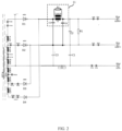
- Fig. 2 shows a more detailed schematic circuit diagram that displays a first example of the secondary circuit 4 of the driver device 1 according to the first embodiment.
- the driver device 1 includes the secondary circuit 4 with the filter circuit 11 arranged in the second load path in a corresponding manner to fig. 1 .
- Fig. 2 provides a particular circuit layout for the filter circuit 11, which will be discussed in more detail.
- the filter circuit 11 of fig. 11 comprises a first capacitor C5, a second capacitor C6, and an inductor.
- the components C5, C6, and L1 are arranged in a ⁇ -filter circuit topology replacing capacitor C4 shown in fig. 5 .
- the main winding L1 of the inductor has first terminal that is connected with the first terminal of the filter circuit 11 and a second terminal that is connected with the second terminal of the filter circuit.
- the main winding L1 is therefore connected in series with a load connected between the second load terminal LED2+ and the common load terminal LED- when a load is connected to the second current path.
- the first capacitor C5 has a first terminal connected with the first terminal of the filter circuit 11, and a second terminal of the first capacitor C5 is connected with the third terminal of the filter circuit 11.
- the second capacitor C6 has a first terminal connected with the second terminal of the filter circuit 11, and a second terminal of the second capacitor C6 is connected with the third terminal of the filter circuit 11.
- the capacitors C5 and C6 are connected in parallel.
- the inductor of the filter circuit 11 includes the main winding L1 and an auxiliary winding L2 AUX .
- a first terminal of the auxiliary winding L2 AUX is connected with a first terminal of the resistor R2 and a second terminal of the auxiliary winding L2 is connected with a second terminal of the resistor R2.
- An electric current through the main winding L2 will induce a voltage in the auxiliary winding L2 AUX .
- the voltage U IND over the resistor R2 may indicate a current flow through the main winding L2 and therefore indicates the load current I LOAD2 output by the second load path via the second load terminal LED2+ to a load connected to the second load terminal LED2+ and the common load terminal LED-.
- the evaluation of the indicator signal U IND by the control circuit 13 may correspond to the embodiment discussed with reference to fig. 1 .
- the control circuit 13 determines that the load is connected via the second load terminal LED2+ and the common load terminal LED-, in case the load current I LOAD is output and the indicator voltage U IND is present at the respective inputs of the control circuit 13 that obtain the indicator voltage U IND . Determining that the indicator voltage U IND is present may correspond to measuring the indicator voltage U IND exceeding a first threshold voltage. In particular, determining that the indicator voltage U IND is present may correspond to determining that the indicator voltage U IND has a voltage value different to o V.
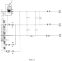
- Fig. 3 depicts a schematic circuit diagram that illustrates a second example of the secondary circuit 4 of the driver device 11 according to the first embodiment.
- the secondary circuit 4 of the driver device 11 includes a filter circuit 11' that differs in its circuit structure and arrangement from the filter circuit 11 displayed in fig. 2 and discussed with reference to fig. 2 .
- the filter circuit 11' comprises an inductor with a main winding L3 and an auxiliary winding L3 AUX .
- a first terminal of the main winding L3 is connected with a first terminal of the filter circuit 11'.
- a second terminal of the main winding L3 is connected with a second terminal of the filter circuit 11'.
- the second example maintains the filter capacitor C4 of the second load path that is connected with the filter capacitor C4 connected to the cathode of the rectifier diode D1 and the cathode of the rectifier diode D4.
- a second terminal of the filter capacitor C4 is connected with the cathode of the rectifier diode D2, the cathode of the rectifier diode D3 and the first load terminal LED1+.
- the filter capacitor C4 may be an electrolytic capacitor.
- a resistor R3 is connected in parallel with the auxiliary winding L3 AUX , and a voltage over the resistor R3 is provided as the indicator voltage U IND to inputs of the control circuit 13 of the secondary circuit 4.
- Fig. 4 illustrates a schematic circuit diagram of a second embodiment of the secondary side circuit 4 of the driver device 1.
- the secondary circuit 4 of the driver device includes a filter circuit 11" that differs in its circuit structure and arrangement from the filter circuit 11 displayed in fig. 2 and corresponds in its general circuit structure to the filter circuit 11' of fig. 3 .
- the embodiment of fig. 4 arranges the filter circuit 11" connected with a first terminal of the filter circuit 11" to a terminal (tap) of the secondary winding L24 of the secondary windings L20 of the transformer 10.
- the second terminal of the filter circuit 11" is connected with the anode of the diode D1 of the second load path.
- the filter circuit 11" comprises an inductor with a main winding L3 an auxiliary winding L3 AUX .
- a first terminal of the induct main winding or L3 is connected with a first terminal of the filter circuit 11".
- a second terminal of the main winding L3 is connected with a second terminal of the filter circuit 11".
- the filter circuit 11" is connected between the transformer 10, in particular between the secondary windings L20 of the transformer 10 and the diode D1.
- the second embodiment maintains the filter capacitor C4 of the second load path that is connected with a first terminal of the filter capacitor C4 to the cathode of the rectifier diode D1 and the cathode of the rectifier diode D4.
- a second terminal of the filter capacitor C4 is connected with the cathode of the rectifier diode D2, the cathode of the rectifier diode D3 and the first load terminal LED1+.
- the filter capacitor C4 may be an electrolytic capacitor.
- a resistor R4 is connected in parallel with the auxiliary winding L3 AUX , and a voltage over the resistor R4 is provided as the indicator voltage U IND to inputs of the control circuit 13 of the secondary circuit 4.
- the main winding L3 may be configured to go into saturation in case a load current I LOAD2 is output via the second load terminal LED2+. In case the main winding L3 goes into saturation, no magnetic flux occurs through the main winding L3 and equally no voltage is induced in the auxiliary winding L3 AUX . Thus, the auxiliary winding L3 AUX provides no measurable voltage to the resistor R4.
- the control circuit 13 of the second embodiment of the filter circuit 11 determines based on the indicator signal, in particular the indicator voltage U IND provided by the auxiliary winding L3 AUX whether the main winding L3 is in saturation.
- the control circuit 13 determines that the load is connected via the second load terminal LED2+ and the common load terminal LED-, in case the load current I LOAD is output, and simultaneously the indicator voltage U IND is not present at the respective inputs of the control circuit 13 that obtains the indicator voltage U IND .
- Determining that the indicator voltage U IND is not present may correspond to measuring the indicator voltage U IND being smaller than a second threshold voltage.
- the second threshold voltage is smaller than the first threshold voltage.
- determining that the indicator voltage U IND is not present may correspond to measuring the indicator voltage U IND is not measurable by the control circuit 13.
- the evaluation circuit 13 may be integrated into control circuit 15 on the primary side (as part of primary circuit 2).
- Fig. 5 shows a schematic circuit diagram that displays an example of a conventional secondary circuit 54 of a known driver device 50 for a comparison with the driver device 1 according to the discussed embodiments.
- the secondary circuit 54 of the known driver device 50 that is implemented in a LLC converter circuit topology of fig. 5 differs from the embodiments shown in figs. 2 , 3 , and 4 by having no filter circuit capable of providing an indicator signal.
- the simple circuit layout of the secondary circuit 54 of fig. 5 does neither acquire nor provide any information, which load terminal of the first and second load terminals LED 1 + and LED2+ of the driver device 50 is connected with an electric load, e.g. a lighting module.
- the lighting module 50 may only provide the capability to implement an emergency shutdown functionality by comparing the primary side voltage over the primary winding L11 of the transformer with a threshold voltage that ensures that neither of the load voltages U LOAD1 and U LOAD2 exceeds an admissible voltage value. Exceeding the admissible voltage value corresponds to determining that an inadmissible overvoltage is present at one of the first load terminal LED1+ and LED2+.
- the lighting module 50 does not provide the capability to calculate the actual output power provided to the connected electric load individually for each of the output channels of the driver device 50.
- the driver device 50 of fig. 5 illustrates at least two key advantages, the driver device 1 provides and which are achieved by any of the particular examples of the filter circuit 11, 11', 11" and its corresponding arrangement in the secondary circuit 4 shown in figs. 2 , 3 , and 4 .
- driver device 1 although the driver device 1 according to the first aspect discusses embodiments using a LLC converter circuit topology with two load output channels and a single filter circuit arranged in one of the two load output channels, the driver device 1 is not limited to this particular structure.
- the driver device 1 may arrange the filter circuit 11, 11', 11" as a first filter circuit 11, 11', 11" in the first load output channel, and a second filter circuit 11, 11', 11" in the second load output channel.
- the circuit topology of the second load output channel that includes the second filter circuit 11, 11', 11" may correspond to the circuit topology of the first load output channel.
- the circuit topology of the second load output channel that includes the second filter circuit 11, 11', 11" and the circuit topology of the second filter circuit 11, 11', 11" may correspond to the circuit topology of any of the embodiments discussed with reference to figs. 2 , 3 , and 4 .
- the driver device 1 may include the secondary circuit 4 comprising multiple (a plurality of) load output channels, e.g. a first load output channel and n second load output channels, wherein n is an integer number of 2 or more.
- the first load output channel and (n-1) second load output channels include each a respective filter circuit 11, 11', 11", e.g. a filter circuit 11, 11', 11" the circuit topology of any of the embodiments discussed with reference to figs. 2 , 3 , and 4 .
- the first load output channel and all n second load output channels include each a respective filter circuit 11, 11', 11", e.g. a filter circuit 11, 11', 11" the circuit topology of any of the embodiments discussed with reference to figs. 2 , 3 , and 4 .
- driver device 1 as well as the building automation system including at least one and more often a large number of such driver devices 1, are susceptible to an advantageous industrial application by implementing an economical and simple way of identifying, which of the multiple load output terminals LED 1 + and LED2+ of the driver device 1 are connected to the load and provide the load current I LOAD , I LOAD1 , I LOAD2 to the load.
Landscapes
- Dc-Dc Converters (AREA)
- Circuit Arrangement For Electric Light Sources In General (AREA)
Abstract
Description
- The invention concerns the field of driver devices for building automation applications, in particular applied in lighting systems. A driver device with plural output channels, e.g. with plural output channels for selectively operating loads at different voltage ranges and exhibiting an improved output channel monitoring is presented.
- Converter devices, e.g. LED converters, implemented in a switch mode power supply (SMPS) circuit topology for generating a load current for driving lighting modules that include one or a plurality of light emitting diodes (LED) form an essential component of temporary lighting systems. The LLC resonant converter topology is a particular example for a converter device applied as a current source to drive LEDs. There exist practical limitations for an achievable load voltage range provided at the load output by the converter device due to considerations concerning device efficiency or switching frequency range, for example.
- In order to overcome the limitations in providing a desired load voltage range, a practical approach is to use a transformer in the LLC resonant converter that provides multiple taps on a secondary winding of the transformer to achieve multiple output voltage ranges using different turn ratios of the transformer.
Fig. 5 of the accompanying drawings displays a general design example for a secondary side circuitry for such an LLC resonant converter device using the transformer with multiple taps on the secondary winding, and alternative load output terminals LED1+ and LED2+ respectively connected with the corresponding taps of the transformer. The LLC resonant converter device has a common load terminal LED- connected with the common return path. The common return path may have a current measuring means for measuring the load current for implementing the current regulation control loop. - Measuring a current in each output channel of the converter device is not necessary for the current regulation and usually avoided for sake of low device complexity, compact design and competitive cost. Measuring the current in each output channel individually may require multiple current transformers portion with differential measurement and is not only expensive with regard to number of components and associated space on the printed circuit board (PCB), but it also results in a much more complex control loop design.
- Nevertheless, for converter devices integrated within a lighting system via a communication network, it may be desirable to implement functions such as power output calculation and reporting the calculated output power via the lighting network, e.g. using a lighting protocol such as digital addressable lighting interface (DALI). This may require determining the load current for each load output individually.
- Thus, it is desirable to provide in the driver device with multiple output channels a capability to determine the output power to a load for different output channels without significantly increasing circuit complexity and cos and cost t.
- The driver device according to
claim 1 and a corresponding building automation system including at least one such driver device provide an advantageous solution addressing the aforementioned issues. - A first aspect concerns the driver device for generating a load current for at least one load. The driver device comprises an isolation barrier for electrically isolating a primary circuit and a secondary circuit of the driver device. The secondary circuit comprises at least a first load terminal and a second load terminal, and the secondary circuit further comprises at least one filter circuit connected to one load terminal of the first load terminal and the second load terminal. The at least one filter circuit is configured to provide a signal that is generated based on the load current output via the load terminal.
- The driver device according to
independent claim 1 represents an economical and simple way of identifying which of the multiple load voltage ranges provided by the output terminals of the driver device actually is connected with the load and in use. The current load voltage output to the load is known by determining which output terminal and which corresponding load voltage range actually is in use. The driver device achieves this without requiring means for measuring the load current in each output channel individually. Therefore, for the purpose of load current regulation, it is still only necessary to measure the total load current, for example, in the common return path of the plural load output channels. Due to dispensing with the need for measuring the current of each output channel individually, the driver device has only modestly increased count of electric components arranged on the PCB, reduced space requirements on the PCB and limited complexity for designing the control loop for regulating the load current output by the driver device, although the load terminal and therefore the load voltage range currently in use is easily determinable. Thus, the driver device may implement further advantages functions such as determining load power output and even implement further reporting functions, which present particular advantages for application in advanced lighting systems. - A further advantageous application of the claimed driver device concerns implementing an individual switch-off of capability for plural load output channels of the driver device. Although a general switch-off capability of the driver device, for example, in case an overvoltage occurs at one of the output terminals without determining individually, at which output channel the overvoltage actually occurs, is generally possible, implementing an individual switch-off capability for the plural output channels becomes possible. This provides a switch-off capability with an increased accuracy and, more advantageous, individually for the plural load output channels. If it is known which of the load output channels is currently active, the switch-off capability may base on voltage thresholds individually predetermined for the plural output channels and their corresponding load voltage ranges. Measuring the current load voltage may be performed by an electric circuitry (primary circuitry) arranged on the primary side of the transformer of the driver device commonly for all output channels. The driver device combines the knowledge on the currently used load output channel and therefore the current load output voltage range based on knowledge on the load voltage terminal currently in use and, thus, the known winding ratio of the transformer currently applicable in order to determine the current load voltage with the measured voltage on the primary side of the transformer. The driver device may select a currently applicable predetermined voltage threshold for overvoltage protection based on knowledge on the load terminal currently in use. Thus, an individual switch-off capability for plural output channels of the driver device becomes implementable with only reduced complexity increase in electronic circuitry.
- The driver device according to an embodiment has the filter circuit including an inductor, and the inductor comprises a main winding, and an auxiliary winding configured to provide a signal induced by a current through a main winding of the inductor.
- According to one embodiment of the driver device, the filter circuit includes a first capacitor and a second capacitor arranged with the inductor of the filter circuit in a π-circuit topology. In that case, the filter circuit may then be further configured to replace a filter capacitor in the secondary circuit of the driver device.
- Further, the driver device, may comprises a transformer for providing the isolation barrier between the a primary circuit and a secondary circuit, and the driver device according to the above explained embodiment may have the secondary circuit comprising at least one diode, with the filter circuit is connected between a secondary winding of the transformer and the diode.
- The driver device according to the above described embodiment may include the evaluation circuit configured to determine that the current is output via the load terminal in case of sensing the signal provided by the auxiliary winding.
- The driver device according to another embodiment includes the inductor configured to go into saturation in case the load current flows through the main winding of the inductor.
- According to this embodiment of the driver device, the driver device may further comprise an evaluation circuit configured to determine whether the current flows through the main winding based on the signal provided by the auxiliary winding, and, further, the evaluation circuit may be configured to determine that the current is output via the load terminal in case of sensing no signal provided by the auxiliary winding.
- According to an embodiment of the driver device, the secondary circuit comprises a sensing means for sensing the load current, wherein the sensing means is connected to a common load terminal for connecting the load.
- The driver device according to an embodiment has the sensing means configured to generate a signal proportional to the load current for controlling the load current in a control loop of the driver device.
- In an embodiment, the driver device may be configured to output the load current in a first voltage range via the first load terminal to the load and to output the load current in a second voltage range via the second load terminal to the load, and the first voltage range and the second voltage range may be different voltage ranges.
- According to an embodiment of the driver device, the driver device is configured to determine a load power output by the driver device based on the load current and the signal provided by the filter circuit, and the driver device is configured to output a communication signal encoding the determined load power.
- The driver device according to an embodiment is configured output a communication signal encoding the determined load power.
- According to an embodiment of the driver device, the driver device is configured to generate the communication signal based on a building automation interface protocol, in particular for a digital addressable lighting interface protocol, a DALI protocol, a DALI-2 protocol or a D4i protocol.
- The driver device according to one embodiment is configured to switch off the driver device in case of determining that a load voltage provided by one of the first load terminal and the second terminal exceeds a preset threshold value based on the signal provided by the filter circuit and based on a voltage measured by the primary circuit.
- The driver may be configured to set the preset threshold value individually for the first load terminal and the second load terminal.
- According to an embodiment of the driver device, the primary circuit is configured to measure the voltage over the primary winding of the transformer, to determine the load terminal that outputs the load current to the load, to determine the load voltage based on the determined load terminal and a winding ratio of the transformer for the determined load terminal, and to compare the determined load voltage with the preset threshold value for the load terminal.
- In an alternative embodiment, the evaluation circuit may be located on the primary side.
- The driver device according to an embodiment is a switch mode power supply (SMPS), in particular a switch mode power supply in LLC resonant converter circuit topology.
- The driver device may be a light driver device, in particular a LED driver device for driving the load that includes at least one LED lighting module.
- A system comprising a driver device and a load, in particular at least one lighting module as the load, according to a second aspect includes at least one driver device according to the first aspect, and the load. The system includes the load connected between a common load terminal and one of the first load terminal and the second load terminal of the driver device.
- The following description of embodiments refers to the attached figures, in which
- Fig. 1
- shows a schematic circuit diagram that illustrates a driver device according to a first embodiment;
- Fig. 2
- shows a schematic circuit diagram that displays a first example of the secondary side circuit of the driver device according to the first embodiment;
- Fig. 3
- shows a schematic circuit diagram that displays a second example of the secondary side circuit of the driver device according to the first embodiment;
- Fig. 4
- shows a schematic circuit diagram that displays an example of the secondary side circuit of the driver device according to the second embodiment; and
- Fig. 5
- shows a schematic circuit diagram that displays an example of the secondary side circuit corresponding to a detail of a driver device according to prior art for comparison with the driver device according to the embodiments.
- In the figures same reference signs denote same or corresponding elements. The discussion of the figures omits a repetitive discussion of same reference signs for different figures wherever deemed possible without adversely affecting comprehensibility.
-
Fig. 1 shows a schematic circuit diagram that illustrates adriver device 1 according to an embodiment. - The
driver device 1 includes electric circuitry comprising a primaryelectric circuit 2 arranged on a primary side of anisolation barrier 3 and secondaryelectric circuit 4 arranged on a secondary side of theisolation barrier 3. - The
isolation barrier 3 galvanically isolates theprimary circuit 2 from thesecondary circuit 4. - The
driver device 1 implements theisolation barrier 3 of thedriver device 1 using atransformer 10. Thetransformer 10 comprisesprimary windings 10, shown is a single primary winding L10, and secondary windings L20. The primary winding 10 is included in theprimary circuit 2. The secondary winding L20 are included in thesecondary circuit 4. - The secondary windings L20 of the
driver device 1 include a first secondary winding L21, a second secondary winding L22, a third secondary winding L23, and a fourth secondary winding L24. - The
driver device 1 is adriver device 1 that generates and outputs a load current ILOAD as load current ILOAD1 in a first load voltage range ULOAD1 or as a second load current ILOAD2 in a second load voltage range ULOAD2. - The
driver device 1 offig. 1 is implemented based on a SMPS topology, and, more specifically, in a LLC converter circuit topology. However, thedriver device 1 is not restricted to an implementation based on the LLC converter circuit topology for providing plural load output channels. - According to the known LLC converter circuit topology, the
primary circuit 2 of thedriver device 1 includes aswitch circuit 5 and subsequent resonant tank circuit 6. - The
switch circuit 5 obtains a DC bus voltage UBUS and may include power switches in a full-bridge topology, in particular four power switches, or power switches, in particular two power switches in a in a half-bridge topology. Theswitch circuit 5 generates an output signal with a rectangular waveform. A difference between the full-bridge topology and the half-bridge topology is that the full-bridge topology generates a signal with a square waveform without DC offset, and an amplitude equal to the bus voltage UBUS. The half-bridge topology emits a signal with the square waveform that is offset by (UBUS / 2). Therefore, the half-bridge topology generates and outputs the signal having half the amplitude of the signal generated by the full bridge topology. - The
switch circuit 5 may include switches implemented by semiconductor switches controlled by a switch control signal with a fundamental switching frequency. Acontrol circuit 15 of theprimary circuit 2 may generate and output the switch control signal to theswitch circuit 5. - The resonant tank circuit 6 obtains the signal output by the
switch circuit 5. The resonant tank circuit 6 may include a resonant capacitor and two inductors: a resonant inductor in series with the resonant capacitor and the primary winding L10 of thetransformer 10, and a magnetizing inductor in parallel with the resonant capacitor and the primary winding L10. The resonant tank circuit 6 performs filtering of the signal provided by theswitch circuit 5 for filtering out the harmonics of the signal and thereby generating a signal having a sine waveform of the fundamental switching frequency of theswitch circuit 5 to an input, in particular the input terminals of the primary winding L11, of thetransformer 10. - The design considerations for the
primary side circuit 2 correspond to the general and well-established design considerations for LLC converter circuits. - The
driver device 1 includes a load interface to an electric load, wherein the load interface includes a common load terminal LED- and a first load terminal LED1+ and a second load terminal LED2+. - The load interface provides an output for the first voltage range ULOAD1 and the corresponding first load current ILOAD1 via the first load terminal LED1+ and the common load terminal LED-.
- The load interface provides an output for the second voltage range ULOAD2 and the corresponding first load current ILOAD2 via the first load terminal LED2+ and the common load terminal LED-.
- The first voltage range ULOAD1 and the second voltage range ULOAD2 may be different voltage ranges. In particular, an upper voltage of the first voltage range ULOAD1 and the second voltage range ULOAD2 may have different voltage values.
- The
secondary circuit 4 of thedriver device 1 may arrange, as depicted infig. 1 , a current sensing means 12 in a common return path of thesecondary circuit 4. The common return path corresponds to the electric connection from the common load terminal LED- to the winding tap connected with one connection each of the elementary secondary windings 22 and 23 of the secondary winding 20 of thetransformer 10. - The current sensing means 12 may generate a current measurement signal corresponding to, e.g. proportional to the load current ILOAD to a
control circuit 13 arranged as a part of thesecondary circuit 4 of thedriver device 1 on the secondary side of thetransformer 10. - The
control circuit 13 may include an integrated circuit (IC), in particular an application specific integrated circuit (ASIC), a microcontroller circuit (µC), a microprocessor or any combination of these circuit elements. - The current sensing means 12 may include a shunt (shunt resistor, measuring resistor) arranged in the common return path. The
secondary circuit 4 may provide a measuring voltage across the shunt resistor directly or indirectly to an analogue input terminal of thecontrol circuit 13 of thedriver device 1. - The
control circuit 13 may generate a return signal based on the measuring voltage that depends on a current value of the load current ILOAD and output the return signal to a transfer means 14 that transmits the return signal over the isolation barrier. - The transfer means 14 may be implemented using an optocoupler or an electric transformer.
- A
control circuit 15 of theprimary circuit 2 of thedriver device 1 receives the return signal from the transfer means 14. Thecontrol circuit 15 may include an integrated circuit (IC), in particular an application specific integrated circuit (ASIC), a microcontroller circuit (µC), a microprocessor or any combination of these circuit elements. - The
control circuit 15 generates a switch control signal for controlling the switches of theswitch circuit 3 of theprimary circuit 2 of thedriver device 1 based on the return signal received from thesecondary circuit 4. - In particular, the
control circuit 15 may implement a controller of a control loop for regulating the load current ILOAD to a preset load current value ILOAD_SET. - The
control circuit 15 may receive the preset load current value ILOAD_SET via a communication signal from acommunication interface 16 of theprimary circuit 2 of thedriver device 1. - The
communication interface 16 may provide a bidirectional communication for thedriver device 1 via communication terminals COM of thedriver device 1 over a communication network based on a predefined communication protocol, e.g. a lighting control protocol including, but not limited to the Digital Addressable Lighting Interface (DALI™) series of protocols. DALI provides a network-based protocol for controlling lighting. - The communication protocol may be a predecessor for DALI™, the 0-10 V lighting control system. Alternatively, an open standard alternative or one proprietary protocol for building automation may be used in addition or alternative to the DALI protocol.
- The DALI™ protocol may include the DALI™ protocol, a DALI-2™ and a D4i™ protocol.
- DALI™ is specified by a series of technical standards in IEC 62386. The DALI™ refers to devices that comply with a DiiA released testing and certification requirements, and are listed as either registered (DALI version-1) or certified (DALI-2) on a DiiA website.
- The
control circuit 16 may generate output signals for transmission via thecommunication module 16 and the communication network. - The communication network may be a wired or a wireless network, e.g. a radio communication network.
- The
secondary circuit 4 shown infig. 1 comprises the secondary windings L20 of thetransformer 10, a first load path including the first load terminal LED1+, a second load path including the output terminal LED2+ and a common return path including the common terminal LED-. - The first load path comprises the secondary winding L22 and L23, and the rectifying diodes D2 and D3, a filter capacitor C3 and an output capacitor C1. The capacitor C3 is an electrolytic capacitor.
- The second load path comprises the secondary windings L21 and L22, L23 and L24, and the rectifying diodes D1 and D4, output capacitors C1 and C2.
- In the embodiment of
fig.1 , afilter circuit 11 replaces the filter capacitor C4 included in the second load path in thesecondary circuit 4 of the knowndriver device 50 as illustrated infig. 5 . - In the specific example of the first embodiment of the invention illustrated in
fig. 1 , a first terminal of thefilter circuit 11 is connected with the cathode of the diode D1 and the cathode of the diode D4. A second terminal of thefilter circuit 11 is connected with the second load terminal LED2+, a first terminal of the output capacitor C2 of the second load path and a first terminal of a resistor R1 (output resistor R1) that is connected between the second load terminal LED2+ and the first load terminal LED1+. - A third terminal of the
filter circuit 11 offig. 1 is connected with the first load terminal LED1+, a first terminal of the output capacitor C1, a first terminal of the filter capacitor C3 of the first load path, a cathode of the rectifier diode D2 and a rectifier diode D3 of the first load path. - The
filter circuit 11 generates an indicator signal UIND based on an electric current throughfilter circuit 11 and provides the indicator signal UIND to thecontrol circuit 13. Thecontrol circuit 13 obtains the indicator signal UIND and evaluates the obtained indicator signal UIND in order to determine whether a first load current ILOAD1 is output via the first load terminal LED1+ or a second load current ILOAD2 is output via the second load terminal LED2+. - The
control circuit 13 includes an evaluation circuit, which determines based on the indicator signal UIND and the current measurement signal provided by the current measurement means 12 arranged in the common return path, whether the first load current ILOAD1 is output via the first load terminal LED1+ or the second load current ILOAD2 is output via the second load terminal LED2+. - A specific circuit example of the
filter circuit 11 will be discussed with reference tofig. 2 . Thefilter circuit 11 is arranged in the current path between Diodes D1 and D4 and the second load terminal LED2+. - In an alternative variant, the
secondary circuit 4 may replace the filter capacitor C3 of the first load path with a further filter circuit 11' in the first load path in an entirely corresponding manner to thefilter circuit 11 in the second load path. In this embodiment, the further filter circuit 11' generates a further indicator signal UIND' based on the an electric current through the further filter circuit 11' and provides the further indicator signal UIND' to thecontrol circuit 13. Thecontrol circuit 13 obtains the indicator signal UIND' and the indicator signal UIND, and evaluates the obtained indicator signals UIND' and UIND in order to determine whether a first load current ILOAD1 is output via the first load terminal LED1+ or a second load current ILOAD2 is output via the second load terminal LED2+. - The
control circuit 13 generates a load indication signal based on the evaluation including information whether the first load current ILOAD1 is output via the first load terminal LED1+ or a second load current ILOAD2 is output via the second load terminal LED2+ and outputs the load indication signal to the transfer means 14. The transfer means 14 transmits the load indication signal over theisolation barrier 3 to thecontrol circuit 15 of theprimary circuit 2 for further processing. -
Fig. 2 shows a more detailed schematic circuit diagram that displays a first example of thesecondary circuit 4 of thedriver device 1 according to the first embodiment. - The
driver device 1 includes thesecondary circuit 4 with thefilter circuit 11 arranged in the second load path in a corresponding manner tofig. 1 .Fig. 2 provides a particular circuit layout for thefilter circuit 11, which will be discussed in more detail. - The
filter circuit 11 of fig. 11 comprises a first capacitor C5, a second capacitor C6, and an inductor. The components C5, C6, and L1 are arranged in a π-filter circuit topology replacing capacitor C4 shown infig. 5 . - In particular, the main winding L1 of the inductor has first terminal that is connected with the first terminal of the
filter circuit 11 and a second terminal that is connected with the second terminal of the filter circuit. The main winding L1 is therefore connected in series with a load connected between the second load terminal LED2+ and the common load terminal LED- when a load is connected to the second current path. The first capacitor C5 has a first terminal connected with the first terminal of thefilter circuit 11, and a second terminal of the first capacitor C5 is connected with the third terminal of thefilter circuit 11. The second capacitor C6 has a first terminal connected with the second terminal of thefilter circuit 11, and a second terminal of the second capacitor C6 is connected with the third terminal of thefilter circuit 11. The capacitors C5 and C6 are connected in parallel. - The inductor of the
filter circuit 11 includes the main winding L1 and an auxiliary winding L2AUX. A first terminal of the auxiliary winding L2 AUX is connected with a first terminal of the resistor R2 and a second terminal of the auxiliary winding L2 is connected with a second terminal of the resistor R2. An electric current through the main winding L2 will induce a voltage in the auxiliary winding L2AUX. The voltage UIND over the resistor R2 may indicate a current flow through the main winding L2 and therefore indicates the load current ILOAD2 output by the second load path via the second load terminal LED2+ to a load connected to the second load terminal LED2+ and the common load terminal LED-. - The evaluation of the indicator signal UIND by the
control circuit 13 may correspond to the embodiment discussed with reference tofig. 1 . - The
control circuit 13 determines that the load is connected via the second load terminal LED2+ and the common load terminal LED-, in case the load current ILOAD is output and the indicator voltage UIND is present at the respective inputs of thecontrol circuit 13 that obtain the indicator voltage UIND. Determining that the indicator voltage UIND is present may correspond to measuring the indicator voltage UIND exceeding a first threshold voltage. In particular, determining that the indicator voltage UIND is present may correspond to determining that the indicator voltage UIND has a voltage value different to o V. -
Fig. 3 depicts a schematic circuit diagram that illustrates a second example of thesecondary circuit 4 of thedriver device 11 according to the first embodiment. - The
secondary circuit 4 of thedriver device 11 includes a filter circuit 11' that differs in its circuit structure and arrangement from thefilter circuit 11 displayed infig. 2 and discussed with reference tofig. 2 . - The filter circuit 11' comprises an inductor with a main winding L3 and an auxiliary winding L3AUX. A first terminal of the main winding L3 is connected with a first terminal of the filter circuit 11'. A second terminal of the main winding L3 is connected with a second terminal of the filter circuit 11'. Contrary to the first example, the second example maintains the filter capacitor C4 of the second load path that is connected with the filter capacitor C4 connected to the cathode of the rectifier diode D1 and the cathode of the rectifier diode D4. A second terminal of the filter capacitor C4 is connected with the cathode of the rectifier diode D2, the cathode of the rectifier diode D3 and the first load terminal LED1+. The filter capacitor C4 may be an electrolytic capacitor.
- A resistor R3 is connected in parallel with the auxiliary winding L3AUX, and a voltage over the resistor R3 is provided as the indicator voltage UIND to inputs of the
control circuit 13 of thesecondary circuit 4. -
Fig. 4 illustrates a schematic circuit diagram of a second embodiment of thesecondary side circuit 4 of thedriver device 1. - The
secondary circuit 4 of the driver device includes afilter circuit 11" that differs in its circuit structure and arrangement from thefilter circuit 11 displayed infig. 2 and corresponds in its general circuit structure to the filter circuit 11' offig. 3 . - Contrary to
figs. 2 and3 , the embodiment offig. 4 arranges thefilter circuit 11" connected with a first terminal of thefilter circuit 11" to a terminal (tap) of the secondary winding L24 of the secondary windings L20 of thetransformer 10. The second terminal of thefilter circuit 11" is connected with the anode of the diode D1 of the second load path. - The
filter circuit 11" comprises an inductor with a main winding L3 an auxiliary winding L3AUX. A first terminal of the induct main winding or L3 is connected with a first terminal of thefilter circuit 11". A second terminal of the main winding L3 is connected with a second terminal of thefilter circuit 11". Thus, thefilter circuit 11" is connected between thetransformer 10, in particular between the secondary windings L20 of thetransformer 10 and the diode D1. - Contrary to the first example of the first embodiment, the second embodiment maintains the filter capacitor C4 of the second load path that is connected with a first terminal of the filter capacitor C4 to the cathode of the rectifier diode D1 and the cathode of the rectifier diode D4. A second terminal of the filter capacitor C4 is connected with the cathode of the rectifier diode D2, the cathode of the rectifier diode D3 and the first load terminal LED1+. The filter capacitor C4 may be an electrolytic capacitor.
- A resistor R4 is connected in parallel with the auxiliary winding L3AUX, and a voltage over the resistor R4 is provided as the indicator voltage UIND to inputs of the
control circuit 13 of thesecondary circuit 4. - The main winding L3 may be configured to go into saturation in case a load current ILOAD2 is output via the second load terminal LED2+. In case the main winding L3 goes into saturation, no magnetic flux occurs through the main winding L3 and equally no voltage is induced in the auxiliary winding L3AUX. Thus, the auxiliary winding L3AUX provides no measurable voltage to the resistor R4. The
control circuit 13 of the second embodiment of thefilter circuit 11 determines based on the indicator signal, in particular the indicator voltage UIND provided by the auxiliary winding L3AUX whether the main winding L3 is in saturation. - Contrary to the first embodiment of the
filter circuit 11 or 11', thecontrol circuit 13 determines that the load is connected via the second load terminal LED2+ and the common load terminal LED-, in case the load current ILOAD is output, and simultaneously the indicator voltage UIND is not present at the respective inputs of thecontrol circuit 13 that obtains the indicator voltage UIND. - Determining that the indicator voltage UIND is not present may correspond to measuring the indicator voltage UIND being smaller than a second threshold voltage. The second threshold voltage is smaller than the first threshold voltage. In particular, determining that the indicator voltage UIND is not present may correspond to measuring the indicator voltage UIND is not measurable by the
control circuit 13. - In an alternative embodiment valid for all examples explained above, the
evaluation circuit 13 may be integrated intocontrol circuit 15 on the primary side (as part of primary circuit 2). -
Fig. 5 shows a schematic circuit diagram that displays an example of a conventional secondary circuit 54 of a knowndriver device 50 for a comparison with thedriver device 1 according to the discussed embodiments. - The secondary circuit 54 of the known
driver device 50 that is implemented in a LLC converter circuit topology offig. 5 differs from the embodiments shown infigs. 2 ,3 , and4 by having no filter circuit capable of providing an indicator signal. The simple circuit layout of the secondary circuit 54 offig. 5 does neither acquire nor provide any information, which load terminal of the first and second load terminals LED1+ and LED2+ of thedriver device 50 is connected with an electric load, e.g. a lighting module. - In consequence of the simple layout, the
lighting module 50 may only provide the capability to implement an emergency shutdown functionality by comparing the primary side voltage over the primary winding L11 of the transformer with a threshold voltage that ensures that neither of the load voltages ULOAD1 and ULOAD2 exceeds an admissible voltage value. Exceeding the admissible voltage value corresponds to determining that an inadmissible overvoltage is present at one of the first load terminal LED1+ and LED2+. - Furthermore, the simple layout of the
driver device 50 offig. 5 , thelighting module 50 does not provide the capability to calculate the actual output power provided to the connected electric load individually for each of the output channels of thedriver device 50. - The
driver device 50 offig. 5 illustrates at least two key advantages, thedriver device 1 provides and which are achieved by any of the particular examples of thefilter circuit secondary circuit 4 shown infigs. 2 ,3 , and4 . - It is noted that, although the
driver device 1 according to the first aspect discusses embodiments using a LLC converter circuit topology with two load output channels and a single filter circuit arranged in one of the two load output channels, thedriver device 1 is not limited to this particular structure. - Alternatively, the
driver device 1 may arrange thefilter circuit first filter circuit second filter circuit - The circuit topology of the second load output channel that includes the
second filter circuit second filter circuit second filter circuit figs. 2 ,3 , and4 . - Alternatively, the
driver device 1 may include thesecondary circuit 4 comprising multiple (a plurality of) load output channels, e.g. a first load output channel and n second load output channels, wherein n is an integer number of 2 or more. In this particular embodiment, the first load output channel and (n-1) second load output channels include each arespective filter circuit filter circuit figs. 2 ,3 , and4 . In a further alternative embodiment, the first load output channel and all n second load output channels include each arespective filter circuit filter circuit figs. 2 ,3 , and4 . - The embodiments of the
driver device 1, as well as the building automation system including at least one and more often a large number ofsuch driver devices 1, are susceptible to an advantageous industrial application by implementing an economical and simple way of identifying, which of the multiple load output terminals LED1+ and LED2+ of thedriver device 1 are connected to the load and provide the load current ILOAD, ILOAD1, ILOAD2 to the load.
Claims (16)
- Driver device for generating a load current (ILOAD1, ILOAD2) for at least one load, the driver device comprisingan isolation barrier (3) for electrically isolating a primary circuit (2) and a secondary circuit (4) of the driver device,the secondary circuit (4) comprises at least a first load terminal (LED1+) and a second load terminal (LED2+), andthe secondary circuit (4) comprising a filter circuit (11 ,11', 11") connected with one load terminal (LED2+) of the first load terminal (LED1+) and the second load terminal (LED2+),the filter circuit (11 ,11', 11") is configured to provide a signal (UIND) that is generated based on the load current (ILOAD1, ILOAD2) output via the connected load terminal (LED2+).
- The driver device according to claim 1, whereinthe filter circuit (11, 11', 11") includes an inductor, andthe inductor comprises a main winding (L1, L2, L3) and an auxiliary winding (L1AUX, L2AUX, L3AUX) configured to provide a signal induced by a current through the main winding (L1, L2, L3) of the inductor.
- The driver device according to claim 2, wherein
the filter circuit (11) includes a first capacitor (C5) and a second capacitor (C6) arranged with the inductor of the filter circuit (11) in a π-circuit topology. - The driver device according to claim 2 or 3, wherein
the evaluation circuit (13) is configured to determine that the current (ILOAD1, ILOAD2) is output via the load terminal (LED2+) connected to the filter circuit (11, 11') in case of sensing the signal (UIND) provided by the auxiliary winding (L1AUX, L2AUX). - The driver device according to any one of the preceding claims, wherein
the secondary circuit (4) comprises at least one diode (D1), and the filter circuit (11, 11') is connected between the diode (D1) and the load terminal (LED2+). - The driver device according to claims 2, wherein
the main winding (L3) is configured to go into saturation in case the load current (ILOAD) flows through the main winding (L3) of the inductor. - The driver device according to claim 6, wherein
the evaluation circuit (13) is configured to determine that the current (ILOAD1, ILOAD2) is output via the connected load terminal (LED2+) in case of sensing no signal provided by the auxiliary winding (L3AUX). - The driver device according to any one of claims 2 toy, wherein
the driver device (1) comprises an evaluation circuit (13) configured to determine whether the current (ILOAD1, ILOAD2) flows through the main winding (L1, L2, L3) based on the signal (UIND) provided by the auxiliary winding (L1AUX, L2AUX, L3AUX). - The driver device according to any of the claims 6 to 8, wherein
the driver (1) comprises a transformer (10) for providing the isolation barrier (3) between the primary circuit (2) and the secondary circuit (4) and at least one diode (D1), and the filter circuit (11") is connected between a secondary winding (L20) of the transformer (10) and the diode (D1). - The driver device according to any one of the preceding claims, wherein
the secondary circuit (4) comprises a sensing means (12) for sensing the load current (ILOAD1, ILOAD2), wherein the sensing means (12) is connected with a common load terminal (LED-) for connecting the load. - The driver device according to claim 10, wherein
the sensing means (12) is configured to generate a signal proportional to the load current (ILOAD) for controlling the load current (ILOAD1, ILOAD2) in a control loop of the driver device. - The driver device according to any one of the preceding claims, wherein
the driver device is configured to output the load current (ILOAD1) in a first voltage range via the first load terminal (LED1+) to the load and to output the load current (ILOAD2) in a second voltage range via the second load terminal (LED2+) to the load. - The driver device according to claim 12, wherein
the first voltage range and the second voltage range differ. - The driver device according to any one of the preceding claims, wherein
the driver device is configured to determine a load power output by the driver device based on the load current (ILOAD1, ILOAD2) and the signal (UIND) provided by the filter circuit (11, 11', 11"). - The driver device according to any one of the preceding claims, whereinthe driver device (1) is configured to switch off the driver device (1) in case of determining that a load voltage (ULOAD1, ULOAD2) provided by one of the first load terminal (LED1+) and the second terminal (LED2+) exceeds a preset threshold value based on the signal (UIND) provided by the filter circuit (11) and based on a voltage (USENSE) measured by the primary circuit (2),wherein the driver device (1) is configured to set the preset threshold value individually for the first load terminal (LED1+) and the second load terminal (LED2+).
- The driver device according to any one of the preceding claims, whereinthe primary circuit (2) is configured to measure the voltage over the primary winding (L10) of the transformer (10),to determine the load terminal (LED1+, LED2+) that outputs the load current (ILOAD1, ILOAD2) to the load,to determine the load voltage (ULOAD) based on the determined load terminal (LED1+, LED2+) and a winding ratio of the transformer (10) for the determined load terminal (LED1+, LED2+), andto compare the determined load voltage (ILOAD1, ILOAD2) with the preset threshold value for the determined load terminal (LED1+, LED2+).
Priority Applications (1)
| Application Number | Priority Date | Filing Date | Title |
|---|---|---|---|
| EP23156221.6A EP4415483B1 (en) | 2023-02-13 | 2023-02-13 | Driver device with plural output channels |
Applications Claiming Priority (1)
| Application Number | Priority Date | Filing Date | Title |
|---|---|---|---|
| EP23156221.6A EP4415483B1 (en) | 2023-02-13 | 2023-02-13 | Driver device with plural output channels |
Publications (2)
| Publication Number | Publication Date |
|---|---|
| EP4415483A1 true EP4415483A1 (en) | 2024-08-14 |
| EP4415483B1 EP4415483B1 (en) | 2025-04-02 |
Family
ID=85227145
Family Applications (1)
| Application Number | Title | Priority Date | Filing Date |
|---|---|---|---|
| EP23156221.6A Active EP4415483B1 (en) | 2023-02-13 | 2023-02-13 | Driver device with plural output channels |
Country Status (1)
| Country | Link |
|---|---|
| EP (1) | EP4415483B1 (en) |
Citations (4)
| Publication number | Priority date | Publication date | Assignee | Title |
|---|---|---|---|---|
| US20110309758A1 (en) * | 2010-06-22 | 2011-12-22 | TPV Electronics (Fujian) Co., Ltd. | Driving circuit for led lamp |
| US20140167634A1 (en) * | 2012-12-17 | 2014-06-19 | Infineon Technologies North America Corp. | Method and Circuit for LED Driver Dimming |
| US9414462B1 (en) * | 2015-03-24 | 2016-08-09 | City University Of Hong Kong | Inductive power transfer for driving multiple organic light emitting diode panels |
| US20220086978A1 (en) * | 2020-09-17 | 2022-03-17 | ERP Power, LLC | Led driver with integrated led lighting for human centric black body dimming |
-
2023
- 2023-02-13 EP EP23156221.6A patent/EP4415483B1/en active Active
Patent Citations (4)
| Publication number | Priority date | Publication date | Assignee | Title |
|---|---|---|---|---|
| US20110309758A1 (en) * | 2010-06-22 | 2011-12-22 | TPV Electronics (Fujian) Co., Ltd. | Driving circuit for led lamp |
| US20140167634A1 (en) * | 2012-12-17 | 2014-06-19 | Infineon Technologies North America Corp. | Method and Circuit for LED Driver Dimming |
| US9414462B1 (en) * | 2015-03-24 | 2016-08-09 | City University Of Hong Kong | Inductive power transfer for driving multiple organic light emitting diode panels |
| US20220086978A1 (en) * | 2020-09-17 | 2022-03-17 | ERP Power, LLC | Led driver with integrated led lighting for human centric black body dimming |
Also Published As
| Publication number | Publication date |
|---|---|
| EP4415483B1 (en) | 2025-04-02 |
Similar Documents
| Publication | Publication Date | Title |
|---|---|---|
| US8080947B2 (en) | Current-sharing transformer and power supply circuit having such current-sharing transformer | |
| US8890424B2 (en) | Illumination device, illumination system, and lamp | |
| EP1988633A1 (en) | Integrated gate driver for controlling and protecting power modules | |
| US20090195169A1 (en) | Power supply circuit with current sharing for driving multiple sets of dc loads | |
| CN105794316A (en) | Driver circuit for lighting means, especially light-emitting diodes | |
| CN101930059A (en) | AC detection circuit for power supply | |
| US8063577B2 (en) | Method and a driver circuit for LED operation | |
| GB2567346A (en) | Ripple current generation circuit | |
| US5930124A (en) | Switching power supply | |
| US11940856B2 (en) | Output load identification method and the apparatus incorporating the same | |
| EP4415483B1 (en) | Driver device with plural output channels | |
| WO2009128025A1 (en) | Switched mode power supply | |
| US20110006605A1 (en) | Current-sharing supply circuit for driving multiple sets of dc loads | |
| US6169491B1 (en) | Multiport power monitor | |
| CN222283525U (en) | LED drive circuit and lamps | |
| US7095158B2 (en) | A/D converter with adjustable internal connection and method for the sameoperating | |
| EP3435740A1 (en) | Lighting system | |
| EP4084583B1 (en) | Circuitry and method for determining a mains voltage in an isolated switched driver device | |
| CN117767776A (en) | Alternating current detection circuit and power converter comprising same | |
| CN215646627U (en) | Power supply | |
| US12040719B2 (en) | Isolated primary side switched converter | |
| CN109194121B (en) | Power supply control circuit | |
| CN221529107U (en) | Constant current source circuit and electronic equipment thereof | |
| JP2011171336A (en) | Led driving circuit | |
| KR101033364B1 (en) | LED Driving Circuit |
Legal Events
| Date | Code | Title | Description |
|---|---|---|---|
| PUAI | Public reference made under article 153(3) epc to a published international application that has entered the european phase |
Free format text: ORIGINAL CODE: 0009012 |
|
| STAA | Information on the status of an ep patent application or granted ep patent |
Free format text: STATUS: THE APPLICATION HAS BEEN PUBLISHED |
|
| AK | Designated contracting states |
Kind code of ref document: A1 Designated state(s): AL AT BE BG CH CY CZ DE DK EE ES FI FR GB GR HR HU IE IS IT LI LT LU LV MC ME MK MT NL NO PL PT RO RS SE SI SK SM TR |
|
| STAA | Information on the status of an ep patent application or granted ep patent |
Free format text: STATUS: REQUEST FOR EXAMINATION WAS MADE |
|
| 17P | Request for examination filed |
Effective date: 20240903 |
|
| RBV | Designated contracting states (corrected) |
Designated state(s): AL AT BE BG CH CY CZ DE DK EE ES FI FR GB GR HR HU IE IS IT LI LT LU LV MC ME MK MT NL NO PL PT RO RS SE SI SK SM TR |
|
| GRAP | Despatch of communication of intention to grant a patent |
Free format text: ORIGINAL CODE: EPIDOSNIGR1 |
|
| STAA | Information on the status of an ep patent application or granted ep patent |
Free format text: STATUS: GRANT OF PATENT IS INTENDED |
|
| INTG | Intention to grant announced |
Effective date: 20250103 |
|
| GRAS | Grant fee paid |
Free format text: ORIGINAL CODE: EPIDOSNIGR3 |
|
| GRAA | (expected) grant |
Free format text: ORIGINAL CODE: 0009210 |
|
| STAA | Information on the status of an ep patent application or granted ep patent |
Free format text: STATUS: THE PATENT HAS BEEN GRANTED |
|
| AK | Designated contracting states |
Kind code of ref document: B1 Designated state(s): AL AT BE BG CH CY CZ DE DK EE ES FI FR GB GR HR HU IE IS IT LI LT LU LV MC ME MK MT NL NO PL PT RO RS SE SI SK SM TR |
|
| REG | Reference to a national code |
Ref country code: GB Ref legal event code: FG4D |
|
| REG | Reference to a national code |
Ref country code: CH Ref legal event code: EP |
|
| P01 | Opt-out of the competence of the unified patent court (upc) registered |
Free format text: CASE NUMBER: APP_11227/2025 Effective date: 20250306 |
|
| REG | Reference to a national code |
Ref country code: IE Ref legal event code: FG4D |
|
| REG | Reference to a national code |
Ref country code: DE Ref legal event code: R096 Ref document number: 602023002639 Country of ref document: DE |
|
| REG | Reference to a national code |
Ref country code: DE Ref legal event code: R084 Ref document number: 602023002639 Country of ref document: DE |
|
| REG | Reference to a national code |
Ref country code: NL Ref legal event code: MP Effective date: 20250402 |
|
| PG25 | Lapsed in a contracting state [announced via postgrant information from national office to epo] |
Ref country code: NL Free format text: LAPSE BECAUSE OF FAILURE TO SUBMIT A TRANSLATION OF THE DESCRIPTION OR TO PAY THE FEE WITHIN THE PRESCRIBED TIME-LIMIT Effective date: 20250402 |
|
| REG | Reference to a national code |
Ref country code: AT Ref legal event code: MK05 Ref document number: 1782581 Country of ref document: AT Kind code of ref document: T Effective date: 20250402 |
|
| PG25 | Lapsed in a contracting state [announced via postgrant information from national office to epo] |
Ref country code: FI Free format text: LAPSE BECAUSE OF FAILURE TO SUBMIT A TRANSLATION OF THE DESCRIPTION OR TO PAY THE FEE WITHIN THE PRESCRIBED TIME-LIMIT Effective date: 20250402 Ref country code: ES Free format text: LAPSE BECAUSE OF FAILURE TO SUBMIT A TRANSLATION OF THE DESCRIPTION OR TO PAY THE FEE WITHIN THE PRESCRIBED TIME-LIMIT Effective date: 20250402 Ref country code: PT Free format text: LAPSE BECAUSE OF FAILURE TO SUBMIT A TRANSLATION OF THE DESCRIPTION OR TO PAY THE FEE WITHIN THE PRESCRIBED TIME-LIMIT Effective date: 20250804 |
|
| REG | Reference to a national code |
Ref country code: LT Ref legal event code: MG9D |
|
| PG25 | Lapsed in a contracting state [announced via postgrant information from national office to epo] |
Ref country code: NO Free format text: LAPSE BECAUSE OF FAILURE TO SUBMIT A TRANSLATION OF THE DESCRIPTION OR TO PAY THE FEE WITHIN THE PRESCRIBED TIME-LIMIT Effective date: 20250702 Ref country code: GR Free format text: LAPSE BECAUSE OF FAILURE TO SUBMIT A TRANSLATION OF THE DESCRIPTION OR TO PAY THE FEE WITHIN THE PRESCRIBED TIME-LIMIT Effective date: 20250703 |
|
| PG25 | Lapsed in a contracting state [announced via postgrant information from national office to epo] |
Ref country code: PL Free format text: LAPSE BECAUSE OF FAILURE TO SUBMIT A TRANSLATION OF THE DESCRIPTION OR TO PAY THE FEE WITHIN THE PRESCRIBED TIME-LIMIT Effective date: 20250402 |
|
| PG25 | Lapsed in a contracting state [announced via postgrant information from national office to epo] |
Ref country code: BG Free format text: LAPSE BECAUSE OF FAILURE TO SUBMIT A TRANSLATION OF THE DESCRIPTION OR TO PAY THE FEE WITHIN THE PRESCRIBED TIME-LIMIT Effective date: 20250402 |
|
| PG25 | Lapsed in a contracting state [announced via postgrant information from national office to epo] |
Ref country code: HR Free format text: LAPSE BECAUSE OF FAILURE TO SUBMIT A TRANSLATION OF THE DESCRIPTION OR TO PAY THE FEE WITHIN THE PRESCRIBED TIME-LIMIT Effective date: 20250402 |
|
| PG25 | Lapsed in a contracting state [announced via postgrant information from national office to epo] |
Ref country code: AT Free format text: LAPSE BECAUSE OF FAILURE TO SUBMIT A TRANSLATION OF THE DESCRIPTION OR TO PAY THE FEE WITHIN THE PRESCRIBED TIME-LIMIT Effective date: 20250402 |
|
| PG25 | Lapsed in a contracting state [announced via postgrant information from national office to epo] |
Ref country code: RS Free format text: LAPSE BECAUSE OF FAILURE TO SUBMIT A TRANSLATION OF THE DESCRIPTION OR TO PAY THE FEE WITHIN THE PRESCRIBED TIME-LIMIT Effective date: 20250702 |
|
| PG25 | Lapsed in a contracting state [announced via postgrant information from national office to epo] |
Ref country code: IS Free format text: LAPSE BECAUSE OF FAILURE TO SUBMIT A TRANSLATION OF THE DESCRIPTION OR TO PAY THE FEE WITHIN THE PRESCRIBED TIME-LIMIT Effective date: 20250802 |
|
| PG25 | Lapsed in a contracting state [announced via postgrant information from national office to epo] |
Ref country code: LV Free format text: LAPSE BECAUSE OF FAILURE TO SUBMIT A TRANSLATION OF THE DESCRIPTION OR TO PAY THE FEE WITHIN THE PRESCRIBED TIME-LIMIT Effective date: 20250402 |
|
| REG | Reference to a national code |
Ref country code: DE Ref legal event code: R097 Ref document number: 602023002639 Country of ref document: DE |
|
| PG25 | Lapsed in a contracting state [announced via postgrant information from national office to epo] |
Ref country code: SM Free format text: LAPSE BECAUSE OF FAILURE TO SUBMIT A TRANSLATION OF THE DESCRIPTION OR TO PAY THE FEE WITHIN THE PRESCRIBED TIME-LIMIT Effective date: 20250402 Ref country code: DK Free format text: LAPSE BECAUSE OF FAILURE TO SUBMIT A TRANSLATION OF THE DESCRIPTION OR TO PAY THE FEE WITHIN THE PRESCRIBED TIME-LIMIT Effective date: 20250402 |
|
| PG25 | Lapsed in a contracting state [announced via postgrant information from national office to epo] |
Ref country code: CZ Free format text: LAPSE BECAUSE OF FAILURE TO SUBMIT A TRANSLATION OF THE DESCRIPTION OR TO PAY THE FEE WITHIN THE PRESCRIBED TIME-LIMIT Effective date: 20250402 |
|
| PG25 | Lapsed in a contracting state [announced via postgrant information from national office to epo] |
Ref country code: EE Free format text: LAPSE BECAUSE OF FAILURE TO SUBMIT A TRANSLATION OF THE DESCRIPTION OR TO PAY THE FEE WITHIN THE PRESCRIBED TIME-LIMIT Effective date: 20250402 |
|
| PG25 | Lapsed in a contracting state [announced via postgrant information from national office to epo] |
Ref country code: SK Free format text: LAPSE BECAUSE OF FAILURE TO SUBMIT A TRANSLATION OF THE DESCRIPTION OR TO PAY THE FEE WITHIN THE PRESCRIBED TIME-LIMIT Effective date: 20250402 |
|
| PG25 | Lapsed in a contracting state [announced via postgrant information from national office to epo] |
Ref country code: IT Free format text: LAPSE BECAUSE OF FAILURE TO SUBMIT A TRANSLATION OF THE DESCRIPTION OR TO PAY THE FEE WITHIN THE PRESCRIBED TIME-LIMIT Effective date: 20250402 |
|
| PLBE | No opposition filed within time limit |
Free format text: ORIGINAL CODE: 0009261 |
|
| STAA | Information on the status of an ep patent application or granted ep patent |
Free format text: STATUS: NO OPPOSITION FILED WITHIN TIME LIMIT |
|
| REG | Reference to a national code |
Ref country code: CH Ref legal event code: L10 Free format text: ST27 STATUS EVENT CODE: U-0-0-L10-L00 (AS PROVIDED BY THE NATIONAL OFFICE) Effective date: 20260211 |
|
| 26N | No opposition filed |
Effective date: 20260105 |
|
| PGFP | Annual fee paid to national office [announced via postgrant information from national office to epo] |
Ref country code: DE Payment date: 20260220 Year of fee payment: 4 |
|
| PGFP | Annual fee paid to national office [announced via postgrant information from national office to epo] |
Ref country code: FR Payment date: 20260224 Year of fee payment: 4 |
|
| PG25 | Lapsed in a contracting state [announced via postgrant information from national office to epo] |
Ref country code: LT Free format text: LAPSE BECAUSE OF FAILURE TO SUBMIT A TRANSLATION OF THE DESCRIPTION OR TO PAY THE FEE WITHIN THE PRESCRIBED TIME-LIMIT Effective date: 20250402 |
|
| PG25 | Lapsed in a contracting state [announced via postgrant information from national office to epo] |
Ref country code: SE Free format text: LAPSE BECAUSE OF FAILURE TO SUBMIT A TRANSLATION OF THE DESCRIPTION OR TO PAY THE FEE WITHIN THE PRESCRIBED TIME-LIMIT Effective date: 20250402 |