EP4415266A1 - Charge pumps, logic circuits including charge pumps, logic devices including logic circuits, and methods of operating logic circuits - Google Patents
Charge pumps, logic circuits including charge pumps, logic devices including logic circuits, and methods of operating logic circuits Download PDFInfo
- Publication number
- EP4415266A1 EP4415266A1 EP23195920.6A EP23195920A EP4415266A1 EP 4415266 A1 EP4415266 A1 EP 4415266A1 EP 23195920 A EP23195920 A EP 23195920A EP 4415266 A1 EP4415266 A1 EP 4415266A1
- Authority
- EP
- European Patent Office
- Prior art keywords
- transistor
- voltage
- gate
- pull
- coupled
- Prior art date
- Legal status (The legal status is an assumption and is not a legal conclusion. Google has not performed a legal analysis and makes no representation as to the accuracy of the status listed.)
- Pending
Links
- 238000000034 method Methods 0.000 title description 8
- 239000003990 capacitor Substances 0.000 claims abstract description 27
- 229910002601 GaN Inorganic materials 0.000 description 28
- 238000010586 diagram Methods 0.000 description 6
- 239000000758 substrate Substances 0.000 description 4
- 238000012986 modification Methods 0.000 description 2
- 230000004048 modification Effects 0.000 description 2
- JMASRVWKEDWRBT-UHFFFAOYSA-N Gallium nitride Chemical compound [Ga]#N JMASRVWKEDWRBT-UHFFFAOYSA-N 0.000 description 1
- 238000007599 discharging Methods 0.000 description 1
- 238000004519 manufacturing process Methods 0.000 description 1
- 239000004557 technical material Substances 0.000 description 1
Images

Classifications
-
- H—ELECTRICITY
- H03—ELECTRONIC CIRCUITRY
- H03K—PULSE TECHNIQUE
- H03K19/00—Logic circuits, i.e. having at least two inputs acting on one output; Inverting circuits
- H03K19/01—Modifications for accelerating switching
- H03K19/017—Modifications for accelerating switching in field-effect transistor circuits
- H03K19/01707—Modifications for accelerating switching in field-effect transistor circuits in asynchronous circuits
- H03K19/01714—Modifications for accelerating switching in field-effect transistor circuits in asynchronous circuits by bootstrapping, i.e. by positive feed-back
-
- H—ELECTRICITY
- H03—ELECTRONIC CIRCUITRY
- H03K—PULSE TECHNIQUE
- H03K19/00—Logic circuits, i.e. having at least two inputs acting on one output; Inverting circuits
- H03K19/0175—Coupling arrangements; Interface arrangements
- H03K19/0185—Coupling arrangements; Interface arrangements using field effect transistors only
- H03K19/018507—Interface arrangements
- H03K19/018535—Interface arrangements of Schottky barrier type [MESFET]
-
- H—ELECTRICITY
- H03—ELECTRONIC CIRCUITRY
- H03K—PULSE TECHNIQUE
- H03K19/00—Logic circuits, i.e. having at least two inputs acting on one output; Inverting circuits
- H03K19/20—Logic circuits, i.e. having at least two inputs acting on one output; Inverting circuits characterised by logic function, e.g. AND, OR, NOR, NOT circuits
-
- H—ELECTRICITY
- H02—GENERATION; CONVERSION OR DISTRIBUTION OF ELECTRIC POWER
- H02M—APPARATUS FOR CONVERSION BETWEEN AC AND AC, BETWEEN AC AND DC, OR BETWEEN DC AND DC, AND FOR USE WITH MAINS OR SIMILAR POWER SUPPLY SYSTEMS; CONVERSION OF DC OR AC INPUT POWER INTO SURGE OUTPUT POWER; CONTROL OR REGULATION THEREOF
- H02M3/00—Conversion of DC power input into DC power output
- H02M3/02—Conversion of DC power input into DC power output without intermediate conversion into AC
- H02M3/04—Conversion of DC power input into DC power output without intermediate conversion into AC by static converters
- H02M3/06—Conversion of DC power input into DC power output without intermediate conversion into AC by static converters using resistors or capacitors, e.g. potential divider
- H02M3/07—Conversion of DC power input into DC power output without intermediate conversion into AC by static converters using resistors or capacitors, e.g. potential divider using capacitors charged and discharged alternately by semiconductor devices with control electrode, e.g. charge pumps
-
- H—ELECTRICITY
- H02—GENERATION; CONVERSION OR DISTRIBUTION OF ELECTRIC POWER
- H02M—APPARATUS FOR CONVERSION BETWEEN AC AND AC, BETWEEN AC AND DC, OR BETWEEN DC AND DC, AND FOR USE WITH MAINS OR SIMILAR POWER SUPPLY SYSTEMS; CONVERSION OF DC OR AC INPUT POWER INTO SURGE OUTPUT POWER; CONTROL OR REGULATION THEREOF
- H02M1/00—Details of apparatus for conversion
- H02M1/0003—Details of control, feedback or regulation circuits
- H02M1/0006—Arrangements for supplying an adequate voltage to the control circuit of converters
-
- H—ELECTRICITY
- H02—GENERATION; CONVERSION OR DISTRIBUTION OF ELECTRIC POWER
- H02M—APPARATUS FOR CONVERSION BETWEEN AC AND AC, BETWEEN AC AND DC, OR BETWEEN DC AND DC, AND FOR USE WITH MAINS OR SIMILAR POWER SUPPLY SYSTEMS; CONVERSION OF DC OR AC INPUT POWER INTO SURGE OUTPUT POWER; CONTROL OR REGULATION THEREOF
- H02M1/00—Details of apparatus for conversion
- H02M1/0003—Details of control, feedback or regulation circuits
- H02M1/0012—Control circuits using digital or numerical techniques
-
- H—ELECTRICITY
- H02—GENERATION; CONVERSION OR DISTRIBUTION OF ELECTRIC POWER
- H02M—APPARATUS FOR CONVERSION BETWEEN AC AND AC, BETWEEN AC AND DC, OR BETWEEN DC AND DC, AND FOR USE WITH MAINS OR SIMILAR POWER SUPPLY SYSTEMS; CONVERSION OF DC OR AC INPUT POWER INTO SURGE OUTPUT POWER; CONTROL OR REGULATION THEREOF
- H02M1/00—Details of apparatus for conversion
- H02M1/08—Circuits specially adapted for the generation of control voltages for semiconductor devices incorporated in static converters
-
- H—ELECTRICITY
- H03—ELECTRONIC CIRCUITRY
- H03K—PULSE TECHNIQUE
- H03K17/00—Electronic switching or gating, i.e. not by contact-making and –breaking
- H03K17/10—Modifications for increasing the maximum permissible switched voltage
- H03K17/102—Modifications for increasing the maximum permissible switched voltage in field-effect transistor switches
-
- H—ELECTRICITY
- H03—ELECTRONIC CIRCUITRY
- H03K—PULSE TECHNIQUE
- H03K17/00—Electronic switching or gating, i.e. not by contact-making and –breaking
- H03K17/51—Electronic switching or gating, i.e. not by contact-making and –breaking characterised by the components used
- H03K17/56—Electronic switching or gating, i.e. not by contact-making and –breaking characterised by the components used by the use, as active elements, of semiconductor devices
- H03K17/687—Electronic switching or gating, i.e. not by contact-making and –breaking characterised by the components used by the use, as active elements, of semiconductor devices the devices being field-effect transistors
- H03K17/6871—Electronic switching or gating, i.e. not by contact-making and –breaking characterised by the components used by the use, as active elements, of semiconductor devices the devices being field-effect transistors the output circuit comprising more than one controlled field-effect transistor
-
- H—ELECTRICITY
- H03—ELECTRONIC CIRCUITRY
- H03K—PULSE TECHNIQUE
- H03K19/00—Logic circuits, i.e. having at least two inputs acting on one output; Inverting circuits
- H03K19/0008—Arrangements for reducing power consumption
- H03K19/0013—Arrangements for reducing power consumption in field effect transistor circuits
-
- H—ELECTRICITY
- H03—ELECTRONIC CIRCUITRY
- H03K—PULSE TECHNIQUE
- H03K19/00—Logic circuits, i.e. having at least two inputs acting on one output; Inverting circuits
- H03K19/01—Modifications for accelerating switching
- H03K19/017—Modifications for accelerating switching in field-effect transistor circuits
- H03K19/01707—Modifications for accelerating switching in field-effect transistor circuits in asynchronous circuits
- H03K19/01721—Modifications for accelerating switching in field-effect transistor circuits in asynchronous circuits by means of a pull-up or down element
-
- H—ELECTRICITY
- H03—ELECTRONIC CIRCUITRY
- H03K—PULSE TECHNIQUE
- H03K19/00—Logic circuits, i.e. having at least two inputs acting on one output; Inverting circuits
- H03K19/02—Logic circuits, i.e. having at least two inputs acting on one output; Inverting circuits using specified components
- H03K19/08—Logic circuits, i.e. having at least two inputs acting on one output; Inverting circuits using specified components using semiconductor devices
- H03K19/094—Logic circuits, i.e. having at least two inputs acting on one output; Inverting circuits using specified components using semiconductor devices using field-effect transistors
- H03K19/0944—Logic circuits, i.e. having at least two inputs acting on one output; Inverting circuits using specified components using semiconductor devices using field-effect transistors using MOSFET or insulated gate field-effect transistors, i.e. IGFET
- H03K19/09441—Logic circuits, i.e. having at least two inputs acting on one output; Inverting circuits using specified components using semiconductor devices using field-effect transistors using MOSFET or insulated gate field-effect transistors, i.e. IGFET of the same canal type
- H03K19/09443—Logic circuits, i.e. having at least two inputs acting on one output; Inverting circuits using specified components using semiconductor devices using field-effect transistors using MOSFET or insulated gate field-effect transistors, i.e. IGFET of the same canal type using a combination of enhancement and depletion transistors
Definitions
- An electronic system includes one or more logic circuits to perform predetermined logical operations.
- Conventional logic circuits may have a relatively slow operation speed to perform the logical operations, or consume a relatively large amount of electric power during the operations, or both, and thus fail to satisfy the requirements of the electronic system.
- Embodiments of the present disclosure relate to charge pumps, logic circuits including charge pumps, logic devices including logic circuits, and methods of operating logic circuits.
- embodiments of the present disclosure relate to GaN-based logic circuits, GaN-based logic devices, and methods of operating GaN-based logic circuits.
- a charge pump for a GaN logic circuit includes a first transistor pulling up an output voltage in response to an input voltage, and a second transistor having a first gate, a second gate, and an output terminal coupled to a gate of the first transistor.
- a GaN logic circuit includes an input node receiving an input voltage, a first pull up transistor pulling up an output voltage in response to the input voltage, and a first depletion mode transistor having a first gate to which a first gate voltage is applied and a second gate to which a second gate voltage is applied.
- the first depletion mode transistor may control the first pull up transistor in response to a gate voltage difference between the first gate voltage and the second gate voltage.
- the logic circuit may further include a capacitor having a first end coupled to the first depletion mode transistor and a second end coupled to the first pull up transistor.
- a logic device includes a logic gate receiving a pair of input signals and performing a logic operation on the received input signals to generate an intermediate signal, and a GaN inverter receiving the intermediate signal and generating an output signal.
- the inverter includes an input node receiving the intermediate signal, a pull up transistor configured to pull up the output signal in response to the intermediate signal, and a depletion mode transistor having a first gate to which a first gate voltage applies and a second gate to which a second gate voltage applies.
- the depletion mode transistor may control the pull up transistor in response to a gate voltage difference between the first gate voltage and the second gate voltage.
- the inverter may further include a capacitor having a first end coupled to the depletion mode transistor and a second end coupled to the pull up transistor.
- a method of operating a GaN logic circuit includes receiving an input voltage, adjusting a pinch off voltage and a first saturation current of a depletion mode transistor in response to a gate voltage difference between a first gate voltage and a second gate voltage, providing the first saturation current to pull down an output voltage to a third level when the input voltage has a first level and to pull up the output voltage to a fourth level when the input voltage has a second level, discharging a second saturation current to ground when the input voltage has the first level, and providing the second saturation current to the depletion mode transistor to adjust the gate voltage difference when the input voltage has the second level.
- the logic circuit may include the depletion mode transistor having a first gate to which the first gate voltage is applied and a second gate to which the second gate voltage is applied, and the first level may be higher than the second level.
- Embodiments of the present disclosure relate to logic circuits, logic devices including one or more logic circuits, and methods of operating logic circuits.
- embodiments of the present disclosure relate to GaN-based logic circuits, GaN-based logic devices, and methods of operating GaN-based logic circuits.
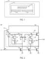
- FIG. 1 illustrates a schematic diagram of a logic device 100 according to an embodiment.
- the logic device 100 may be a driver for a power transistor, or a latch, or any one of various logic gates such as a NAND gate, a NOR gate, a buffer, an OR gate, and an AND gate.
- the logic device 100 in FIG. 1 includes one or more logic circuits 110.
- the logic circuit 110 may be an inverter.
- the logic circuit 110 in FIG. 1 includes a charge pump 140, and the charge pump 140 may include a depletion mode transistor 120, a first current source 136, and a second current source 138.
- the depletion mode transistor 120 has first and second gates to control a pinch off voltage and a first saturation current thereof.
- the depletion mode transistor 120 keeps each of the pinch off voltage and the first saturation current substantially constant when an input voltage has a first level.
- the first current source 136 in FIG. 1 discharges a second saturation current
- the second current source 138 in FIG. 1 discharges the first saturation current.
- Each of the first saturation current and the second saturation current may have a relatively small magnitude, thereby reducing power consumption of the logic circuit 110 during the operation.
- the first current source 136 in FIG. 1 provides the second saturation current to the depletion mode transistor 120 to increase a gate voltage difference between a first gate voltage applied to the first gate and a second gate voltage applied to the second gate.
- Each of the pinch off voltage and the first saturation current of the depletion mode transistor 120 increases in a given manner with the increased gate voltage difference to increase an output voltage of the logic circuit 110, which further increases the gate voltage difference and the first saturation current in turn.
- Such a positive feedback makes the output voltage of the logic circuit 110 reach a target level in a relatively short period, thereby increasing an operation speed of the logic circuit 110.
- FIG. 2 illustrates an inverter 210 suitable for use as the logic circuit 110 in FIG. 1 according to an embodiment.
- the inverter 210 in FIG. 2 includes a substrate including GaN on which one or more circuit elements are implemented.
- the inverter 210 in FIG. 2 includes a first transistor 220, a second transistor 212, a third transistor 222, a first resistor 214, and a second resistor 224.
- the first transistor 220 in FIG. 2 is a depletion mode transistor having first and second gates G1 and G2 to adjust a saturation current and a pinch off voltage thereof.
- the saturation current and the pinch off voltage of the first transistor 220 may be adjusted in response to a gate voltage difference V G1 -V G2 between a first gate voltage V G1 applied to the first gate G1 and a second gate voltage V G2 applied to the second gate G2.
- the third transistor 222 in FIG. 2 is a depletion mode transistor having a drain coupled to a second node N2, a source coupled to a first end of the second resistor 224, and a gate coupled to a second end of the second resistor 224.
- the inverter 210 in FIG. 2 further includes a first pull up transistor 218, a second pull up transistor 232, a capacitor 216, a first pull down transistor 226, a second pull down transistor 228, and a third pull down transistor 230.
- the first pull up transistor 218 in FIG. 2 is an enhancement mode transistor having a drain coupled to a power supply voltage V DD , a source coupled to an output node N OUT generating an output signal (e.g., an output voltage) OUT, and a gate coupled to the second node N2.
- the second pull down transistor 228 in FIG. 2 is a depletion mode transistor having a drain coupled to the power supply voltage V DD , a source coupled to the first node N1, and a gate coupled to an input node N IN receiving an input signal (e.g., an input voltage) IN.
- the capacitor 216 in FIG. 2 has a first end coupled to the first node N1 and a second end coupled to the output node N OUT .
- the first pull down transistor 226 in FIG. 2 is an enhancement mode transistor having a drain coupled to the second end of the first resistor 214, a source coupled to ground, and a gate coupled to the input node N IN .
- the third pull down transistor 230 in FIG. 2 is an enhancement mode transistor having a drain coupled to the output node N OUT , a source coupled to the ground, and a gate coupled to the input node N IN .
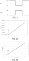
- FIG. 3 is a waveform diagram illustrating an operation of the inverter 210 in FIG. 2 according to an embodiment.
- FIGS. 4A and 4B illustrate a first saturation current I sat1 and a pinch off voltage V pinch of the first transistor 220 in FIG. 2 , respectively, as a function of a gate voltage difference V G1 -V G2 between a first gate voltage V G1 and a second gate voltage V G2 of the first transistor 220 according to an embodiment.
- the first pull down transistor 226 When the input voltage IN has a first level indicative of a logic high value (e.g., V DD ), the first pull down transistor 226 is turned on to pull down the first gate voltage V G1 of the first transistor 220 to ground (e.g., 0V) or substantially ground, and the second pull up transistor 232 is turned on to pull up a voltage at the first node N1 to the power supply voltage V DD .
- the second transistor 212 and the first resistor 214 together function as a first current source 236 to discharge a second saturation current I sat2 to ground.
- the first resistor 214 has a relatively high resistance value to make the second saturation current I sat2 have a relatively small magnitude.
- the resistance value of the first resistor 214 may be in a range from to 10 kohm (kS2) to 1 Megaohm (M ⁇ ).
- kS2 kohm
- M ⁇ Megaohm
- the first gate voltage V G1 at the first gate G1 of the first transistor 220 is maintained at a level equal to or substantially equal to ground.
- the second gate G2 of the first transistor 220 is coupled to ground, and thus a second gate voltage V G2 has a level equal to or substantially equal to ground.
- the first saturation current I sat1 of the first transistor 220 has a substantially constant and relatively small magnitude (e.g., about 1 ⁇ A) and the pinch off voltage V pinch of the first transistor 220 has a substantially constant and relatively small level (e.g., about 0.5V).
- the first saturation current I sat1 having a relatively small magnitude flows through the first transistor 220, and a voltage at the second node N2 becomes substantially equal to the pinch off voltage V pinch having a relatively small level.
- the second pull down transistor 228 When the input voltage IN has the first level, the second pull down transistor 228 is turned on.
- the first saturation current I sat1 has a relatively small magnitude, and the third transistor 222 and the second resistor 224 together function as a second current source 238 to discharge the first saturation current I sat1 to ground.
- the voltage at the second node N2 is maintained at a level sufficiently small to keep the first pull up transistor 218 turned off.
- the voltage at the second node N2 may be maintained at a level substantially equal to or less than 50%, 25%, or 10% of a threshold voltage of the first pull up transistor 218.
- the output voltage OUT is pulled down to a third level (e.g., ground or substantially ground). Since each of the first saturation current I sat1 and the second saturation current I sat2 has a relatively small magnitude, power consumption of the inverter 210 may be reduced during the operation.
- the second pull up transistor 232 When the input voltage IN has a second level indicative of a logic low value (e.g., 0 V), the second pull up transistor 232 is turned off to make the first end of the capacitor 216 float.
- the first, second, and third pull down transistors 226, 228, and 230 are turned off to electrically disconnect the second ends of the first and second resistors 214 and 224 from the ground and make the second end of the capacitor 216 float.
- the second saturation current I sat2 flows through the second transistor 212 and the first resistor 214 into the first gate G1 of the first transistor 220 to increase the first gate voltage V G1 as well as the gate voltage difference V G1 -V G2 . Referring to FIGS.
- the charge pump 240 includes the first transistor 220, the first pull up transistor 218, the capacitor 216, the first current source 236, the second current source 238, the first node N1, the second node N2, and the output node N OUT .
- the first transistor 220 provides the first saturation current I sat1 to pull up the output voltage OUT from the third level (e.g., 0V) to a fourth level (e.g., the power supply voltage V DD ) when the input voltage has the second level.
- the first saturation current I sat1 flowing through the first transistor 220 increases and the third transistor 222 and the second resistors 224 are electrically disconnected from the ground, and thus the voltage at the gate of the first pull up transistor 218 increases sufficiently to turn on the first pull up transistor 218.
- the first pull up transistor 218 increases the output voltage OUT at the output node N OUT , which increases a voltage at the second end of the capacitor 216 coupled to the output node N OUT as well as a voltage at the first end of the capacitor 216.
- a voltage at the first node N1 coupled to the first end of the capacitor 216 also increases to further increase the first gate voltage V G1 of the first transistor 220, leading to a further increase in the gate voltage difference V G1 -V G2 as well as a further increase in the first saturation current I sat1 in turn.
- Such a positive feedback of the charge pump 240 makes the output voltage OUT reach the power supply voltage V DD in a relatively short period, thereby increasing an operation speed of the inverter 210.
- the first saturation current I sat1 of the first transistor 220 has a substantially constant and relatively small magnitude and the pinch off voltage V pinch of the first transistor 220 has a substantially constant and relatively small level when the gate voltage difference V G1 -V G2 is less than a threshold voltage Vth.
- each of the first saturation current I sat1 and the pinch off voltage V pinch of the first transistor 220 increases substantially linearly with the gate voltage difference V G1 - V G2 when the gate voltage difference V G1 - V G2 is equal to or greater than the threshold voltage Vth.
- embodiments of the present disclosure are not limited thereto.
- each of the first saturation current I sat1 and the pinch off voltage V pinch of the first transistor 220 increases substantially exponentially with the gate voltage difference V G1 - V G2 when the gate voltage difference V G1 - V G2 is equal to or greater than the threshold voltage Vth, thereby making the output voltage OUT reach the power supply voltage V DD faster compared to when the first saturation current I sat1 increases substantially linearly with the gate voltage difference V G1 - V G2 .
- FIG. 5 illustrates an inverter 510 suitable for use as the inverter 110 in FIG. 1 according to an embodiment.
- FIG. 6 is a waveform diagram illustrating an operation of the inverter 510 according to an embodiment.
- the inverter 510 in FIG. 5 includes similar elements to those of the inverter 210 in FIG. 2 , and an operation of the inverter 510 in FIG. 5 is similar to that of the inverter 210 in FIG. 2 . Accordingly, detailed descriptions on these similar elements and operation may be omitted in the following disclosure in the interest of brevity.
- the inverter 510 of FIG. 5 differs from the inverter 210 of FIG. 2 in that the inverter 510 includes a first pull up transistor 518 having a drain coupled to a second power supply voltage Vcc, rather than a first power supply voltage V DD .
- the operation of the inverter 510 in FIG. 5 differs from that of the inverter 210 in FIG. 2 in that the output voltage OUT has a level substantially equal to the second power supply voltage Vcc, rather than the first power supply voltage V DD , when the input voltage IN has a logic low value (e.g., 0V).
- the second power supply voltage Vcc has a level different from that of the first power supply voltage V DD , such that the inverter 510 functions as a level shifter circuit.
- the second power supply voltage Vcc may have a level that is greater (e.g., about twice as great as) than that of the first power supply voltage V DD .
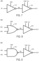
- FIG. 7 illustrates a buffer 700 according to an embodiment.
- the buffer 700 includes a substrate including GaN on which one or more circuit elements are implemented.
- the buffer 700 in FIG. 7 includes a first inverter 710 and a second inverter 720.
- the first inverter 710 may be similar or identical to the inverter 210 in FIG. 2
- the second inverter 720 may be similar or identical to the inverter 510 in FIG. 5 .
- the first inverter 710 in FIG. 7 receives an input signal (e.g., an input voltage) IN and outputs an intermediate signal (e.g., an intermediate voltage) IM changing between ground and a first power supply voltage V DD .
- the second inverter 720 in FIG. 7 receives the intermediate signal IM and outputs an output signal (e.g., an output voltage) OUT changing between ground and a second power supply voltage Vcc.
- FIG. 8 illustrates an OR gate 800 according to an embodiment.
- the OR gate 800 includes a substrate including GaN on which one or more circuit elements are implemented.
- the OR gate 800 in FIG. 8 includes a NOR gate 810 and an inverter 820.
- the inverter 820 may be similar or identical to the inverter 510 in FIG. 5 .
- the NOR gate 850 in FIG. 8 receives a first input signal IN1 and a second input signal IN2 and performs an NOR operation on the first and second input signals IN1 and IN2 to output an intermediate signal IM changing between ground and a first power supply voltage V DD .
- the inverter 820 in FIG. 8 receives the intermediate signal IM and outputs an output signal OUT changing between ground and a second power supply voltage Vcc.
- FIG. 9 illustrates an AND gate 900 according to an embodiment.
- the AND gate 900 includes a substrate including GaN on which one or more circuit elements are implemented.
- the AND gate 900 in FIG. 9 includes a NAND gate 910 and an inverter 920.
- the inverter 920 may be similar or identical to the inverter 510 in FIG. 5 .
- the NAND gate 910 in FIG. 9 receives a first input signal IN1 and a second input signal IN2 and performs a NAND operation on the first and second input signals IN1 and IN2 to output an intermediate signal IM changing between ground and a first power supply voltage V DD .
- the inverter 920 in FIG. 9 receives the intermediate signal IM and outputs an output signal OUT changing between ground and a second power supply voltage Vcc.
- a charge pump for a GaN logic circuit comprising: a first transistor configured to pull up an output voltage in response to an input voltage; and a second transistor having a first gate, a second gate, and an output terminal coupled to a gate of the first transistor.
- the charge pump of embodiment 3 or 4 further comprising: a first current source configured to discharge a second saturation current to ground when the input voltage has a first level, and to provide the second saturation current to the depletion mode transistor to adjust the gate voltage difference when the input voltage has a second level.
- the depletion mode transistor is a first depletion mode transistor
- the first current source includes: a first resistor having a first end and a second end, the second end coupled to the first gate of the first depletion mode transistor; and a second depletion mode transistor having a source coupled to the first end of the first resistor, a gate coupled to the second end of the first resistor, and a drain coupled to the drain of the first depletion mode transistor.
- the second current source includes: a second resistor having a first end and a second end; and a third depletion mode transistor having a drain coupled to the source of the first depletion mode transistor, a source coupled to the first end of the second resistor, a gate coupled to the second end of the second resistor.
- a GaN logic circuit comprising: an input node configured to receive an input voltage; a first pull up transistor configured to pull up an output voltage in response to the input voltage; a first depletion mode transistor having a first gate to which a first gate voltage is applied and a second gate to which a second gate voltage is applied, the first depletion mode transistor configured to control the first pull up transistor in response to a gate voltage difference between the first gate voltage and the second gate voltage; and a capacitor having a first end coupled to the first depletion mode transistor and a second end coupled to the first pull up transistor.
- the first current source includes: a first resistor having a first end and a second end, the second end coupled to the first gate of the first depletion mode transistor; and a second depletion mode transistor having a source coupled to the first end of the first resistor, a gate coupled to the second end of the first resistor, and a drain coupled to a drain of the first depletion mode transistor.
- a logic device comprising: a logic gate configured to receive a pair of input signals and performs a logic operation on the received input signals to generate an intermediate signal; and a GaN inverter configured to receive the intermediate signal and generate an output signal, the inverter comprising: an input node configured to receive the intermediate signal; a pull up transistor configured to pull up the output signal in response to the intermediate signal; a depletion mode transistor having a first gate to which a first gate voltage applies and a second gate to which a second gate voltage applies, the depletion mode transistor configured to control the pull up transistor in response to a gate voltage difference between the first gate voltage and the second gate voltage; and a capacitor having a first end coupled to the depletion mode transistor and a second end coupled to the pull up transistor.
- the term "include” and its variants may be interpreted as meaning that an embodiment includes stated features, while not necessarily excluding the presence of other features that are not explicitly stated.
Landscapes
- Engineering & Computer Science (AREA)
- Computer Hardware Design (AREA)
- Physics & Mathematics (AREA)
- Computing Systems (AREA)
- General Engineering & Computer Science (AREA)
- Mathematical Physics (AREA)
- Power Engineering (AREA)
- Logic Circuits (AREA)
Abstract
A GaN logic circuit (210) may include an input node (IN) receiving an input voltage, a first pull up transistor (218) pulling up an output voltage (OUT) in response to the input voltage (IN), and a first depletion mode transistor (220) having a first gate (G1) to which a first gate voltage (VG1) is applied and a second gate (G2) to which a second gate voltage (VG2) is applied. The first depletion mode transistor (220) may control the first pull up transistor (218) in response to a gate voltage difference (VG1 - VG2) between the first gate voltage (VG1) and the second gate voltage (VG2). The logic device may further include a capacitor (216) having a first end coupled to the first depletion mode transistor and a second end coupled to the first pull up transistor.
Description
- An electronic system includes one or more logic circuits to perform predetermined logical operations. Conventional logic circuits may have a relatively slow operation speed to perform the logical operations, or consume a relatively large amount of electric power during the operations, or both, and thus fail to satisfy the requirements of the electronic system.
- Embodiments of the present disclosure relate to charge pumps, logic circuits including charge pumps, logic devices including logic circuits, and methods of operating logic circuits. In particular, embodiments of the present disclosure relate to GaN-based logic circuits, GaN-based logic devices, and methods of operating GaN-based logic circuits.
- In an embodiment, a charge pump for a GaN logic circuit includes a first transistor pulling up an output voltage in response to an input voltage, and a second transistor having a first gate, a second gate, and an output terminal coupled to a gate of the first transistor.
- In an embodiment, a GaN logic circuit includes an input node receiving an input voltage, a first pull up transistor pulling up an output voltage in response to the input voltage, and a first depletion mode transistor having a first gate to which a first gate voltage is applied and a second gate to which a second gate voltage is applied. The first depletion mode transistor may control the first pull up transistor in response to a gate voltage difference between the first gate voltage and the second gate voltage. The logic circuit may further include a capacitor having a first end coupled to the first depletion mode transistor and a second end coupled to the first pull up transistor.
- In an embodiment, a logic device includes a logic gate receiving a pair of input signals and performing a logic operation on the received input signals to generate an intermediate signal, and a GaN inverter receiving the intermediate signal and generating an output signal. The inverter includes an input node receiving the intermediate signal, a pull up transistor configured to pull up the output signal in response to the intermediate signal, and a depletion mode transistor having a first gate to which a first gate voltage applies and a second gate to which a second gate voltage applies. The depletion mode transistor may control the pull up transistor in response to a gate voltage difference between the first gate voltage and the second gate voltage. The inverter may further include a capacitor having a first end coupled to the depletion mode transistor and a second end coupled to the pull up transistor.
- In an embodiment, a method of operating a GaN logic circuit includes receiving an input voltage, adjusting a pinch off voltage and a first saturation current of a depletion mode transistor in response to a gate voltage difference between a first gate voltage and a second gate voltage, providing the first saturation current to pull down an output voltage to a third level when the input voltage has a first level and to pull up the output voltage to a fourth level when the input voltage has a second level, discharging a second saturation current to ground when the input voltage has the first level, and providing the second saturation current to the depletion mode transistor to adjust the gate voltage difference when the input voltage has the second level. The logic circuit may include the depletion mode transistor having a first gate to which the first gate voltage is applied and a second gate to which the second gate voltage is applied, and the first level may be higher than the second level.
-
-
FIG. 1 illustrates a schematic diagram of a logic device according to an embodiment. -
FIG. 2 illustrates an inverter suitable for use as the logic circuit inFIG. 1 according to an embodiment. -
FIG. 3 is a waveform diagram illustrating an operation of the inverter inFIG. 2 according to an embodiment. -
FIGS. 4A and 4B illustrate a saturation current and a pinch off voltage of a depletion mode transistor, respectively, as a function of a gate voltage difference between a first gate voltage and a second gate voltage of the depletion mode transistor according to an embodiment. -
FIG. 5 illustrates an inverter suitable for use as the logic circuit inFIG. 1 according to an embodiment. -
FIG. 6 is a waveform diagram illustrating an operation of the inverter inFIG. 5 according to an embodiment. -
FIG. 7 illustrates a buffer according to an embodiment. -
FIG. 8 illustrates an OR gate according to an embodiment. -
FIG. 9 illustrates an AND gate according to an embodiment. - Embodiments of the present disclosure relate to logic circuits, logic devices including one or more logic circuits, and methods of operating logic circuits. In particular, embodiments of the present disclosure relate to GaN-based logic circuits, GaN-based logic devices, and methods of operating GaN-based logic circuits.
- A detailed description of embodiments is provided below along with accompanying figures. The scope of this disclosure is limited by the claims and encompasses numerous alternatives, modifications and equivalents. Although steps of various processes are presented in a given order, embodiments are not necessarily limited to being performed in the listed order. In some embodiments, certain operations may be performed simultaneously, in an order other than the described order, or not performed at all.
- Numerous specific details are set forth in the following description. These details are provided to promote a thorough understanding of the scope of this disclosure by way of specific examples, and embodiments may be practiced according to the claims without some of these specific details. Accordingly, the specific embodiments of this disclosure are illustrative, and are not intended to be exclusive or limiting. For the purpose of clarity, technical material that is known in the technical fields related to this disclosure has not been described in detail so that the disclosure is not unnecessarily obscured.
-
FIG. 1 illustrates a schematic diagram of alogic device 100 according to an embodiment. For example, thelogic device 100 may be a driver for a power transistor, or a latch, or any one of various logic gates such as a NAND gate, a NOR gate, a buffer, an OR gate, and an AND gate. - The
logic device 100 inFIG. 1 includes one ormore logic circuits 110. For example, thelogic circuit 110 may be an inverter. - The
logic circuit 110 inFIG. 1 includes acharge pump 140, and thecharge pump 140 may include adepletion mode transistor 120, a firstcurrent source 136, and a secondcurrent source 138. In an embodiment, thedepletion mode transistor 120 has first and second gates to control a pinch off voltage and a first saturation current thereof. - When an input voltage has a first level, the
depletion mode transistor 120 keeps each of the pinch off voltage and the first saturation current substantially constant when an input voltage has a first level. The firstcurrent source 136 inFIG. 1 discharges a second saturation current, and the secondcurrent source 138 inFIG. 1 discharges the first saturation current. Each of the first saturation current and the second saturation current may have a relatively small magnitude, thereby reducing power consumption of thelogic circuit 110 during the operation. - When the input voltage has a second level, the first
current source 136 inFIG. 1 provides the second saturation current to thedepletion mode transistor 120 to increase a gate voltage difference between a first gate voltage applied to the first gate and a second gate voltage applied to the second gate. Each of the pinch off voltage and the first saturation current of thedepletion mode transistor 120 increases in a given manner with the increased gate voltage difference to increase an output voltage of thelogic circuit 110, which further increases the gate voltage difference and the first saturation current in turn. Such a positive feedback makes the output voltage of thelogic circuit 110 reach a target level in a relatively short period, thereby increasing an operation speed of thelogic circuit 110. -
FIG. 2 illustrates aninverter 210 suitable for use as thelogic circuit 110 inFIG. 1 according to an embodiment. In an embodiment, theinverter 210 inFIG. 2 includes a substrate including GaN on which one or more circuit elements are implemented. - The
inverter 210 inFIG. 2 includes afirst transistor 220, asecond transistor 212, athird transistor 222, afirst resistor 214, and asecond resistor 224. In an embodiment, thefirst transistor 220 inFIG. 2 is a depletion mode transistor having first and second gates G1 and G2 to adjust a saturation current and a pinch off voltage thereof. For example, the saturation current and the pinch off voltage of thefirst transistor 220 may be adjusted in response to a gate voltage difference VG1-VG2 between a first gate voltage VG1 applied to the first gate G1 and a second gate voltage VG2 applied to the second gate G2. Thesecond transistor 212 inFIG. 2 is a depletion mode transistor having a drain coupled to a first node N1, a source coupled to a first end of thefirst resistor 214, and a gate coupled to a second end of thefirst resistor 214. Thethird transistor 222 inFIG. 2 is a depletion mode transistor having a drain coupled to a second node N2, a source coupled to a first end of thesecond resistor 224, and a gate coupled to a second end of thesecond resistor 224. - The
inverter 210 inFIG. 2 further includes a firstpull up transistor 218, a second pull uptransistor 232, acapacitor 216, a first pull downtransistor 226, a second pull downtransistor 228, and a third pull downtransistor 230. The firstpull up transistor 218 inFIG. 2 is an enhancement mode transistor having a drain coupled to a power supply voltage VDD, a source coupled to an output node NOUT generating an output signal (e.g., an output voltage) OUT, and a gate coupled to the second node N2. The second pull uptransistor 232 inFIG. 2 is a depletion mode transistor having a drain coupled to the power supply voltage VDD, a source coupled to the first node N1, and a gate coupled to an input node NIN receiving an input signal (e.g., an input voltage) IN. Thecapacitor 216 inFIG. 2 has a first end coupled to the first node N1 and a second end coupled to the output node NOUT. The first pull downtransistor 226 inFIG. 2 is an enhancement mode transistor having a drain coupled to the second end of thefirst resistor 214, a source coupled to ground, and a gate coupled to the input node NIN. The second pull downtransistor 228 inFIG. 2 is an enhancement mode transistor having a drain coupled to the second end of thesecond resistor 224, a source coupled to the ground, and a gate coupled to the input node NIN. The third pull downtransistor 230 inFIG. 2 is an enhancement mode transistor having a drain coupled to the output node NOUT, a source coupled to the ground, and a gate coupled to the input node NIN. -
FIG. 3 is a waveform diagram illustrating an operation of theinverter 210 inFIG. 2 according to an embodiment.FIGS. 4A and 4B illustrate a first saturation current Isat1 and a pinch off voltage Vpinch of thefirst transistor 220 inFIG. 2 , respectively, as a function of a gate voltage difference VG1-VG2 between a first gate voltage VG1 and a second gate voltage VG2 of thefirst transistor 220 according to an embodiment. - When the input voltage IN has a first level indicative of a logic high value (e.g., VDD), the first pull down
transistor 226 is turned on to pull down the first gate voltage VG1 of thefirst transistor 220 to ground (e.g., 0V) or substantially ground, and the second pull uptransistor 232 is turned on to pull up a voltage at the first node N1 to the power supply voltage VDD. Thesecond transistor 212 and thefirst resistor 214 together function as a firstcurrent source 236 to discharge a second saturation current Isat2 to ground. In an embodiment, thefirst resistor 214 has a relatively high resistance value to make the second saturation current Isat2 have a relatively small magnitude. For example, the resistance value of thefirst resistor 214 may be in a range from to 10 kohm (kS2) to 1 Megaohm (MΩ). As a result, the first gate voltage VG1 at the first gate G1 of thefirst transistor 220 is maintained at a level equal to or substantially equal to ground. The second gate G2 of thefirst transistor 220 is coupled to ground, and thus a second gate voltage VG2 has a level equal to or substantially equal to ground. - Referring to
FIGS. 4A and 4B , when the first gate voltage VG1 and a second gate voltage VG2 each have a level substantially equal to 0V, the first saturation current Isat1 of thefirst transistor 220 has a substantially constant and relatively small magnitude (e.g., about 1 µA) and the pinch off voltage Vpinch of thefirst transistor 220 has a substantially constant and relatively small level (e.g., about 0.5V). As a result, referring back toFIG. 2 , the first saturation current Isat1 having a relatively small magnitude flows through thefirst transistor 220, and a voltage at the second node N2 becomes substantially equal to the pinch off voltage Vpinch having a relatively small level. - When the input voltage IN has the first level, the second pull down
transistor 228 is turned on. The first saturation current Isat1 has a relatively small magnitude, and thethird transistor 222 and thesecond resistor 224 together function as a secondcurrent source 238 to discharge the first saturation current Isat1 to ground. As a result, the voltage at the second node N2 is maintained at a level sufficiently small to keep the first pull uptransistor 218 turned off. In an embodiment, the voltage at the second node N2 may be maintained at a level substantially equal to or less than 50%, 25%, or 10% of a threshold voltage of the first pull uptransistor 218. Since the first pull uptransistor 218 is turned off and the third pull downtransistor 230 is turned on in response to the input voltage IN having the first level, the output voltage OUT is pulled down to a third level (e.g., ground or substantially ground). Since each of the first saturation current Isat1 and the second saturation current Isat2 has a relatively small magnitude, power consumption of theinverter 210 may be reduced during the operation. - When the input voltage IN has a second level indicative of a logic low value (e.g., 0 V), the second pull up
transistor 232 is turned off to make the first end of thecapacitor 216 float. The first, second, and third pull downtransistors second resistors capacitor 216 float. The second saturation current Isat2 flows through thesecond transistor 212 and thefirst resistor 214 into the first gate G1 of thefirst transistor 220 to increase the first gate voltage VG1 as well as the gate voltage difference VG1-VG2. Referring toFIGS. 4A and 4B , when the increased gate voltage difference VG1-VG2 reaches a threshold voltage Vth of thefirst transistor 220, the first saturation current Isat1 and the pinch off voltage Vpinch of thefirst transistor 220 start to increase substantially linearly with the gate voltage difference VG1-VG2. - Referring back to
FIG. 2 , thecharge pump 240 includes thefirst transistor 220, the first pull uptransistor 218, thecapacitor 216, the firstcurrent source 236, the secondcurrent source 238, the first node N1, the second node N2, and the output node NOUT. Thefirst transistor 220 provides the first saturation current Isat1 to pull up the output voltage OUT from the third level (e.g., 0V) to a fourth level (e.g., the power supply voltage VDD) when the input voltage has the second level. For example, the first saturation current Isat1 flowing through thefirst transistor 220 increases and thethird transistor 222 and thesecond resistors 224 are electrically disconnected from the ground, and thus the voltage at the gate of the first pull uptransistor 218 increases sufficiently to turn on the first pull uptransistor 218. The first pull uptransistor 218 increases the output voltage OUT at the output node NOUT, which increases a voltage at the second end of thecapacitor 216 coupled to the output node NOUT as well as a voltage at the first end of thecapacitor 216. A voltage at the first node N1 coupled to the first end of thecapacitor 216 also increases to further increase the first gate voltage VG1 of thefirst transistor 220, leading to a further increase in the gate voltage difference VG1-VG2 as well as a further increase in the first saturation current Isat1 in turn. Such a positive feedback of thecharge pump 240 makes the output voltage OUT reach the power supply voltage VDD in a relatively short period, thereby increasing an operation speed of theinverter 210. - According to the embodiment shown in
FIGS. 4A and 4B , the first saturation current Isat1 of thefirst transistor 220 has a substantially constant and relatively small magnitude and the pinch off voltage Vpinch of thefirst transistor 220 has a substantially constant and relatively small level when the gate voltage difference VG1-VG2 is less than a threshold voltage Vth. In contrast, each of the first saturation current Isat1 and the pinch off voltage Vpinch of thefirst transistor 220 increases substantially linearly with the gate voltage difference VG1 - VG2 when the gate voltage difference VG1 - VG2 is equal to or greater than the threshold voltage Vth. However, embodiments of the present disclosure are not limited thereto. In other embodiments, each of the first saturation current Isat1 and the pinch off voltage Vpinch of thefirst transistor 220 increases substantially exponentially with the gate voltage difference VG1 - VG2 when the gate voltage difference VG1 - VG2 is equal to or greater than the threshold voltage Vth, thereby making the output voltage OUT reach the power supply voltage VDD faster compared to when the first saturation current Isat1 increases substantially linearly with the gate voltage difference VG1 - VG2. Details of the structure of thefirst transistor 220 and the fabrication method thereof can be found in pendingU.S. Patent Application Ser. No. 17/819,980, entitled "INTEGRATED DEPLETION AND ENHANCEMENT MODE GALLIUM NITRIDE HIGH-ELECTRON MOBILITY TRANSISTORS" and filed on August 16, 2022 U.S. Patent Application Ser. No. 17/902,463, entitled "HIGH-ELECTRON-MOBILITY TRANSISTOR" and filed on February 2, 2022 -
FIG. 5 illustrates aninverter 510 suitable for use as theinverter 110 inFIG. 1 according to an embodiment.FIG. 6 is a waveform diagram illustrating an operation of theinverter 510 according to an embodiment. Theinverter 510 inFIG. 5 includes similar elements to those of theinverter 210 inFIG. 2 , and an operation of theinverter 510 inFIG. 5 is similar to that of theinverter 210 inFIG. 2 . Accordingly, detailed descriptions on these similar elements and operation may be omitted in the following disclosure in the interest of brevity. - The
inverter 510 ofFIG. 5 differs from theinverter 210 ofFIG. 2 in that theinverter 510 includes a first pull uptransistor 518 having a drain coupled to a second power supply voltage Vcc, rather than a first power supply voltage VDD. As a result, the operation of theinverter 510 inFIG. 5 differs from that of theinverter 210 inFIG. 2 in that the output voltage OUT has a level substantially equal to the second power supply voltage Vcc, rather than the first power supply voltage VDD, when the input voltage IN has a logic low value (e.g., 0V). In an embodiment, the second power supply voltage Vcc has a level different from that of the first power supply voltage VDD, such that theinverter 510 functions as a level shifter circuit. For example, the second power supply voltage Vcc may have a level that is greater (e.g., about twice as great as) than that of the first power supply voltage VDD. -
FIG. 7 illustrates abuffer 700 according to an embodiment. In an embodiment, thebuffer 700 includes a substrate including GaN on which one or more circuit elements are implemented. - The
buffer 700 inFIG. 7 includes afirst inverter 710 and asecond inverter 720. In an embodiment, thefirst inverter 710 may be similar or identical to theinverter 210 inFIG. 2 , and thesecond inverter 720 may be similar or identical to theinverter 510 inFIG. 5 . For example, thefirst inverter 710 inFIG. 7 receives an input signal (e.g., an input voltage) IN and outputs an intermediate signal (e.g., an intermediate voltage) IM changing between ground and a first power supply voltage VDD. Thesecond inverter 720 inFIG. 7 receives the intermediate signal IM and outputs an output signal (e.g., an output voltage) OUT changing between ground and a second power supply voltage Vcc. -
FIG. 8 illustrates anOR gate 800 according to an embodiment. In an embodiment, theOR gate 800 includes a substrate including GaN on which one or more circuit elements are implemented. - The OR
gate 800 inFIG. 8 includes a NORgate 810 and aninverter 820. In an embodiment, theinverter 820 may be similar or identical to theinverter 510 inFIG. 5 . For example, the NOR gate 850 inFIG. 8 receives a first input signal IN1 and a second input signal IN2 and performs an NOR operation on the first and second input signals IN1 and IN2 to output an intermediate signal IM changing between ground and a first power supply voltage VDD. Theinverter 820 inFIG. 8 receives the intermediate signal IM and outputs an output signal OUT changing between ground and a second power supply voltage Vcc. -
FIG. 9 illustrates an ANDgate 900 according to an embodiment. In an embodiment, the ANDgate 900 includes a substrate including GaN on which one or more circuit elements are implemented. - The AND
gate 900 inFIG. 9 includes aNAND gate 910 and aninverter 920. In an embodiment, theinverter 920 may be similar or identical to theinverter 510 inFIG. 5 . For example, theNAND gate 910 inFIG. 9 receives a first input signal IN1 and a second input signal IN2 and performs a NAND operation on the first and second input signals IN1 and IN2 to output an intermediate signal IM changing between ground and a first power supply voltage VDD. Theinverter 920 inFIG. 9 receives the intermediate signal IM and outputs an output signal OUT changing between ground and a second power supply voltage Vcc. - Aspects of the present disclosure have been described in conjunction with the specific embodiments thereof that are proposed as examples. Numerous alternatives, modifications, and variations to the embodiments as set forth herein may be made without departing from the scope of the claims set forth below. Accordingly, embodiments as set forth herein are intended to be illustrative and not limiting.
- In summary, the following embodiments are explicitly disclosed.
- A charge pump for a GaN logic circuit, comprising: a first transistor configured to pull up an output voltage in response to an input voltage; and a second transistor having a first gate, a second gate, and an output terminal coupled to a gate of the first transistor.
- The charge pump of
embodiment 1, wherein the second transistor is a depletion mode transistor, and the output terminal of the depletion mode transistor is controlled by a gate voltage difference between a first gate voltage applied to the first gate and a second gate voltage applied to the second gate, the charge pump further comprising: a capacitor having a first end coupled to the second transistor and a second end coupled to the first transistor. - The charge pump of
embodiment 2, wherein the depletion mode transistor adjusts a pinch off voltage and a first saturation current in response to the gate voltage difference. - The charge pump of
embodiment 3, wherein the output terminal of the depletion mode transistor is a source coupled to the gate of the first transistor, and the depletion mode transistor further has a drain coupled to the first end of the capacitor. - The charge pump of
embodiment - The charge pump of
embodiment 5, wherein the depletion mode transistor is a first depletion mode transistor, and wherein the first current source includes: a first resistor having a first end and a second end, the second end coupled to the first gate of the first depletion mode transistor; and a second depletion mode transistor having a source coupled to the first end of the first resistor, a gate coupled to the second end of the first resistor, and a drain coupled to the drain of the first depletion mode transistor. - The charge pump of
embodiment 6, further comprising: a second current source configured to discharge the first saturation current to the ground when the input voltage has the first level. - The charge pump of
embodiment 7, wherein the second current source includes: a second resistor having a first end and a second end; and a third depletion mode transistor having a drain coupled to the source of the first depletion mode transistor, a source coupled to the first end of the second resistor, a gate coupled to the second end of the second resistor. - A GaN logic circuit, comprising: an input node configured to receive an input voltage; a first pull up transistor configured to pull up an output voltage in response to the input voltage; a first depletion mode transistor having a first gate to which a first gate voltage is applied and a second gate to which a second gate voltage is applied, the first depletion mode transistor configured to control the first pull up transistor in response to a gate voltage difference between the first gate voltage and the second gate voltage; and a capacitor having a first end coupled to the first depletion mode transistor and a second end coupled to the first pull up transistor.
- The GaN logic circuit of embodiment 9, wherein the first depletion mode transistor adjusts a pinch off voltage and a first saturation current in response to the gate voltage difference, and provides the first saturation current to pull down the output voltage to a third level when the input voltage has a first level and to pull up the output voltage to a fourth level when the input voltage has a second level, the first level being higher than the second level.
- The GaN logic circuit of embodiment 10, wherein the first depletion mode transistor keeps each of the pinch off voltage and the first saturation current substantially constant to pull down the output voltage to the third level when the input voltage has the first level, and increases each of the pinch off voltage and the first saturation current substantially linearly with the gate voltage difference to pull up the output voltage to the fourth level when the input voltage has the second level.
- The GaN logic circuit of one of embodiments 10 or 11, wherein a power supply voltage has the fourth level, and the first pull up transistor is further configured to receive the first saturation current from the first depletion transistor and to pull up the output voltage to the power supply voltage when the input voltage has the second level, the circuit further comprising: a second pull up transistor configured to pull up a voltage at the first end of the capacitor to the power supply voltage when the input voltage has the first level, and make the first end of the capacitor float when the input voltage has the second level.
- The GaN logic circuit of embodiment 12, wherein the first pull up transistor has a drain coupled to the power supply voltage, a gate coupled to a source of the first depletion mode transistor, and a source coupled to the output node, and wherein the second pull up transistor has a drain coupled to the power supply voltage, a gate coupled to the input node, and a source coupled to the first end of the capacitor.
- The GaN logic circuit of one of embodiments 9 to 13, wherein the power supply voltage is a first power supply voltage, the circuit further comprising: a second pull up transistor configured to pull up a voltage at the first end of the capacitor to a second power supply voltage when the input voltage has the first level, and make the first end of the capacitor float when the input voltage has the second level, the second power supply voltage having a level different from that of the first power supply voltage.
- The GaN logic circuit of one of embodiments 9 to 14, further comprising: a first current source configured to discharge a second saturation current to ground when the input voltage has the first level, and to provide the second saturation current to the first depletion mode transistor to adjust the gate voltage difference when the input voltage has the second level.
- The GaN logic circuit of embodiment 15, wherein the first current source includes: a first resistor having a first end and a second end, the second end coupled to the first gate of the first depletion mode transistor; and a second depletion mode transistor having a source coupled to the first end of the first resistor, a gate coupled to the second end of the first resistor, and a drain coupled to a drain of the first depletion mode transistor.
- The GaN logic circuit of embodiment 16, wherein the first resistor has a resistance value in a range from 10 kohm (kS2) to 1 Megaohm (MΩ).
- The GaN logic circuit of embodiment 16 or 17, further comprising: a first pull down transistor having a drain coupled to the second end of the first resistor, a gate coupled to the input node, and a source coupled to the ground.
- The GaN logic circuit of one of embodiment 15 to 18, further comprising: a second current source configured to discharge the first saturation current to the ground when the input voltage has the first level.
- A logic device, comprising: a logic gate configured to receive a pair of input signals and performs a logic operation on the received input signals to generate an intermediate signal; and a GaN inverter configured to receive the intermediate signal and generate an output signal, the inverter comprising: an input node configured to receive the intermediate signal; a pull up transistor configured to pull up the output signal in response to the intermediate signal; a depletion mode transistor having a first gate to which a first gate voltage applies and a second gate to which a second gate voltage applies, the depletion mode transistor configured to control the pull up transistor in response to a gate voltage difference between the first gate voltage and the second gate voltage; and a capacitor having a first end coupled to the depletion mode transistor and a second end coupled to the pull up transistor.
- At least in the embodiments above, the term "include" and its variants may be interpreted as meaning that an embodiment includes stated features, while not necessarily excluding the presence of other features that are not explicitly stated.
Claims (15)
- A charge pump for a GaN logic circuit, comprising:a first transistor configured to pull up an output voltage in response to an input voltage; anda second transistor having a first gate, a second gate, and an output terminal coupled to a gate of the first transistor.
- The charge pump of claim 1, wherein the second transistor is a depletion mode transistor, and the output terminal of the depletion mode transistor is controlled by a gate voltage difference between a first gate voltage applied to the first gate and a second gate voltage applied to the second gate, the charge pump further comprising:
a capacitor having a first end coupled to the second transistor and a second end coupled to the first transistor. - The charge pump of claim 2, wherein the depletion mode transistor adjusts a pinch off voltage and a first saturation current in response to the gate voltage difference, the output terminal of the depletion mode transistor preferably being a source coupled to the gate of the first transistor and the depletion mode transistor preferably further having a drain coupled to the first end of the capacitor.
- The charge pump of claim 3, further comprising:
a first current source configured to discharge a second saturation current to ground when the input voltage has a first level, and to provide the second saturation current to the depletion mode transistor to adjust the gate voltage difference when the input voltage has a second level. - The charge pump of claim 4, wherein the depletion mode transistor is a first depletion mode transistor, and
wherein the first current source includes:a first resistor having a first end and a second end, the second end coupled to the first gate of the first depletion mode transistor; anda second depletion mode transistor having a source coupled to the first end of the first resistor, a gate coupled to the second end of the first resistor, and a drain coupled to the drain of the first depletion mode transistor. - The charge pump of claim 5, further comprising:
a second current source configured to discharge the first saturation current to the ground when the input voltage has the first level,
wherein the second current source preferably includes:a second resistor having a first end and a second end; anda third depletion mode transistor having a drain coupled to the source of the first depletion mode transistor, a source coupled to the first end of the second resistor, a gate coupled to the second end of the second resistor. - A GaN logic circuit, comprising:an input node configured to receive an input voltage;the charge pump of one of claims 1 to 6,wherein the first transistor of the charge pump is a first pull up transistor of the GaN logic circuit, the first pull up transistor being configured to pull up an output voltage in response to the input voltage, andwherein the second transistor of the charge pump is a first depletion mode transistor of the GaN logic circuit, the first depletion mode transistor having the first gate for receiving a first gate voltage and the second gate for receiving a second gate voltage; anda capacitor having a first end coupled to the first depletion mode transistor and a second end coupled to the first pull up transistor,wherein the first depletion mode transistor of the GaN logic circuit is configured to control the first pull up transistor in response to a gate voltage difference between the first gate voltage and the second gate voltage.
- The GaN logic circuit of claim 7, wherein the first depletion mode transistor adjusts a pinch off voltage and a first saturation current in response to the gate voltage difference, and provides the first saturation current to pull down the output voltage to a third level when the input voltage has a first level and to pull up the output voltage to a fourth level when the input voltage has a second level, the first level being higher than the second level.
- The GaN logic circuit of claim 8, wherein the first depletion mode transistor keeps each of the pinch off voltage and the first saturation current substantially constant to pull down the output voltage to the third level when the input voltage has the first level, and increases each of the pinch off voltage and the first saturation current substantially linearly with the gate voltage difference to pull up the output voltage to the fourth level when the input voltage has the second level.
- The GaN logic circuit of claim 8 or 9, wherein a power supply voltage has the fourth level, andwherein the first pull up transistor is further configured to receive the first saturation current from the first depletion transistor and to pull up the output voltage to the power supply voltage when the input voltage has the second level,the circuit further comprising:
a second pull up transistor configured to pull up a voltage at the first end of the capacitor to the power supply voltage when the input voltage has the first level, and make the first end of the capacitor float when the input voltage has the second level. - The GaN logic circuit of claim 10, wherein the first pull up transistor has a drain coupled to the power supply voltage, a gate coupled to a source of the first depletion mode transistor, and a source coupled to the output node, and
wherein the second pull up transistor has a drain coupled to the power supply voltage, a gate coupled to the input node, and a source coupled to the first end of the capacitor. - The GaN logic circuit of claim 10 or 11, wherein the power supply voltage is a first power supply voltage, and
wherein the second pull up transistor is further configured to pull up the voltage at the first end of the capacitor to a second power supply voltage when the input voltage has the first level, the second power supply voltage having a level different from that of the first power supply voltage. - The GaN logic circuit of one of claims 7 to 12, further comprising:
a first current source configured to discharge a second saturation current to ground when the input voltage has the first level, and to provide the second saturation current to the first depletion mode transistor to adjust the gate voltage difference when the input voltage has the second level. - The GaN logic circuit of claim 13, wherein the first current source includes:a first resistor having a first end and a second end, the second end coupled to the first gate of the first depletion mode transistor, the first resistor preferably having a resistance value in a range from 10 kohm (kS2) to 1 Megaohm (MS2); anda second depletion mode transistor having a source coupled to the first end of the first resistor, a gate coupled to the second end of the first resistor, and a drain coupled to a drain of the first depletion mode transistor, andthe GaN logic circuit preferably further comprising a first pull down transistor having a drain coupled to the second end of the first resistor, a gate coupled to the input node, and a source coupled to the ground.
- A logic device, comprising:a logic gate configured to receive a pair of input signals and performs a logic operation on the received input signals to generate an intermediate signal; anda GaN inverter configured to receive the intermediate signal and generate an output signal, the GaN inverter comprising the GaN logic circuit of one of claims 7 to 14,wherein the input node is configured to receive the intermediate signal as the input voltage, andwherein the first pull up transistor is configured to pull up the output signal in response to the intermediate signal.
Applications Claiming Priority (1)
| Application Number | Priority Date | Filing Date | Title |
|---|---|---|---|
| US18/167,279 US12323143B2 (en) | 2023-02-10 | 2023-02-10 | Charge pumps, logic circuits including charge pumps, logic devices including logic circuits, and methods of operating logic circuits |
Publications (1)
| Publication Number | Publication Date |
|---|---|
| EP4415266A1 true EP4415266A1 (en) | 2024-08-14 |
Family
ID=87971976
Family Applications (1)
| Application Number | Title | Priority Date | Filing Date |
|---|---|---|---|
| EP23195920.6A Pending EP4415266A1 (en) | 2023-02-10 | 2023-09-07 | Charge pumps, logic circuits including charge pumps, logic devices including logic circuits, and methods of operating logic circuits |
Country Status (4)
| Country | Link |
|---|---|
| US (1) | US12323143B2 (en) |
| EP (1) | EP4415266A1 (en) |
| CN (1) | CN118487489A (en) |
| TW (1) | TWI897190B (en) |
Families Citing this family (1)
| Publication number | Priority date | Publication date | Assignee | Title |
|---|---|---|---|---|
| US12323143B2 (en) * | 2023-02-10 | 2025-06-03 | Globalfoundries U.S. Inc. | Charge pumps, logic circuits including charge pumps, logic devices including logic circuits, and methods of operating logic circuits |
Citations (3)
| Publication number | Priority date | Publication date | Assignee | Title |
|---|---|---|---|---|
| US9461126B2 (en) * | 2013-09-13 | 2016-10-04 | Semiconductor Energy Laboratory Co., Ltd. | Transistor, clocked inverter circuit, sequential circuit, and semiconductor device including sequential circuit |
| US20210211128A1 (en) * | 2020-01-06 | 2021-07-08 | Diodes Incorporated | Gate Drive Apparatus and Control Method |
| CN113922812A (en) * | 2021-10-13 | 2022-01-11 | 西交利物浦大学 | NAND gate logic circuit and preparation method thereof |
Family Cites Families (17)
| Publication number | Priority date | Publication date | Assignee | Title |
|---|---|---|---|---|
| US7518352B2 (en) * | 2007-05-11 | 2009-04-14 | Freescale Semiconductor, Inc. | Bootstrap clamping circuit for DC/DC regulators and method thereof |
| JPWO2011064955A1 (en) * | 2009-11-30 | 2013-04-11 | パナソニック株式会社 | Bidirectional switch |
| JP2012004253A (en) * | 2010-06-15 | 2012-01-05 | Panasonic Corp | Bidirectional switch, two-wire ac switch, switching power circuit, and method for driving bidirectional switch |
| FR2988535B1 (en) | 2012-03-23 | 2014-03-07 | Soitec Silicon On Insulator | TRANSISTOR LOAD PUMP CIRCUIT WITH DOUBLE PHASE DOORS AND METHOD OF OPERATING SAID CIRCUIT. |
| US9985626B2 (en) * | 2015-01-30 | 2018-05-29 | Navitas Semiconductor, Inc. | Bidirectional GaN switch with built-in bias supply and integrated gate drivers |
| US10530360B2 (en) * | 2016-02-29 | 2020-01-07 | Infineon Technologies Austria Ag | Double gate transistor device and method of operating |
| US11257811B2 (en) * | 2017-07-14 | 2022-02-22 | Cambridge Enterprise Limited | Power semiconductor device with an auxiliary gate structure |
| US10536070B1 (en) | 2018-08-01 | 2020-01-14 | Infineon Technologies Ag | Driver for switching gallium nitride (GaN) devices |
| JP7357206B2 (en) * | 2018-11-08 | 2023-10-06 | パナソニックIpマネジメント株式会社 | Electrical equipment and multilevel inverters |
| US10554112B1 (en) | 2019-04-04 | 2020-02-04 | Navitas Semiconductor, Inc. | GaN driver circuit |
| US10454481B1 (en) | 2019-04-04 | 2019-10-22 | Navitas Semiconductor, Inc | GaN logic circuits |
| US12382651B2 (en) * | 2019-05-07 | 2025-08-05 | Cambridge Gan Devices Limited | Power semiconductor device with an auxiliary gate structure |
| US12396196B2 (en) * | 2022-08-19 | 2025-08-19 | Globalfoundries U.S. Inc. | Protective structure with depletion-mode and enhancement-mode transistors |
| US12206321B2 (en) * | 2022-09-21 | 2025-01-21 | Semiconductor Components Industries, Llc | Bootstrap clamp circuit and method |
| US12143112B2 (en) * | 2022-10-12 | 2024-11-12 | Globalfoundries U.S. Inc. | Circuit for controlling the slew rate of a transistor |
| US20240145469A1 (en) * | 2022-10-26 | 2024-05-02 | Globalfoundries U.S. Inc. | One time programmable device |
| US12323143B2 (en) * | 2023-02-10 | 2025-06-03 | Globalfoundries U.S. Inc. | Charge pumps, logic circuits including charge pumps, logic devices including logic circuits, and methods of operating logic circuits |
-
2023
- 2023-02-10 US US18/167,279 patent/US12323143B2/en active Active
- 2023-09-07 EP EP23195920.6A patent/EP4415266A1/en active Pending
-
2024
- 2024-01-10 TW TW113101091A patent/TWI897190B/en active
- 2024-01-10 CN CN202410041828.5A patent/CN118487489A/en active Pending
Patent Citations (3)
| Publication number | Priority date | Publication date | Assignee | Title |
|---|---|---|---|---|
| US9461126B2 (en) * | 2013-09-13 | 2016-10-04 | Semiconductor Energy Laboratory Co., Ltd. | Transistor, clocked inverter circuit, sequential circuit, and semiconductor device including sequential circuit |
| US20210211128A1 (en) * | 2020-01-06 | 2021-07-08 | Diodes Incorporated | Gate Drive Apparatus and Control Method |
| CN113922812A (en) * | 2021-10-13 | 2022-01-11 | 西交利物浦大学 | NAND gate logic circuit and preparation method thereof |
Also Published As
| Publication number | Publication date |
|---|---|
| US20240275385A1 (en) | 2024-08-15 |
| CN118487489A (en) | 2024-08-13 |
| US12323143B2 (en) | 2025-06-03 |
| KR20240125438A (en) | 2024-08-19 |
| TWI897190B (en) | 2025-09-11 |
| TW202448126A (en) | 2024-12-01 |
Similar Documents
| Publication | Publication Date | Title |
|---|---|---|
| KR930003926B1 (en) | Semiconductor integrated circuit | |
| CN105446923B (en) | Differential driver with pull-up booster and pull-down booster | |
| KR100991383B1 (en) | Output driver of semiconductor device | |
| US7812660B2 (en) | Level shift circuit | |
| JP3905401B2 (en) | Semiconductor integrated circuit | |
| US10903840B2 (en) | Pad tracking circuit for high-voltage input-tolerant output buffer | |
| US5684738A (en) | Analog semiconductor memory device having multiple-valued comparators and floating-gate transistor | |
| US10284201B1 (en) | High range positive voltage level shifter using low voltage devices | |
| WO2019042189A1 (en) | Shift register circuit, driving method, gate drive circuit, and display device | |
| US20230238953A1 (en) | Circuit and method | |
| KR100528858B1 (en) | Amplitude converting circuit | |
| US12323143B2 (en) | Charge pumps, logic circuits including charge pumps, logic devices including logic circuits, and methods of operating logic circuits | |
| CN113196660A (en) | Comparator for power and high speed applications | |
| US8482317B2 (en) | Comparator and method with adjustable speed and power consumption | |
| US7969217B2 (en) | Output buffer with slew-rate enhancement output stage | |
| US20120098584A1 (en) | Circuit and method for improvement of a level shifter | |
| US20230188127A1 (en) | Pre-driven bootstrapping drivers | |
| US7679419B2 (en) | Level shifter device with write assistance and method thereof | |
| US7468600B2 (en) | Voltage regulation unit with Zener diode and voltage regulation device thereof | |
| US9831879B2 (en) | Low core power leakage structure in IO receiver during IO power down | |
| US12149232B2 (en) | Multi-voltage bootstrapping drivers | |
| US6556048B1 (en) | High speed low skew LVTTL output buffer with invert capability | |
| CN221765975U (en) | A voltage comparison circuit | |
| JP2000165227A (en) | Logic output circuit | |
| US6548995B1 (en) | High speed bias voltage generating circuit |
Legal Events
| Date | Code | Title | Description |
|---|---|---|---|
| PUAI | Public reference made under article 153(3) epc to a published international application that has entered the european phase |
Free format text: ORIGINAL CODE: 0009012 |
|
| STAA | Information on the status of an ep patent application or granted ep patent |
Free format text: STATUS: REQUEST FOR EXAMINATION WAS MADE |
|
| 17P | Request for examination filed |
Effective date: 20230907 |
|
| AK | Designated contracting states |
Kind code of ref document: A1 Designated state(s): AL AT BE BG CH CY CZ DE DK EE ES FI FR GB GR HR HU IE IS IT LI LT LU LV MC ME MK MT NL NO PL PT RO RS SE SI SK SM TR |