EP4415052A1 - Semiconductor switching device - Google Patents
Semiconductor switching device Download PDFInfo
- Publication number
- EP4415052A1 EP4415052A1 EP24155182.9A EP24155182A EP4415052A1 EP 4415052 A1 EP4415052 A1 EP 4415052A1 EP 24155182 A EP24155182 A EP 24155182A EP 4415052 A1 EP4415052 A1 EP 4415052A1
- Authority
- EP
- European Patent Office
- Prior art keywords
- region
- cell
- jfet
- semiconductor device
- width
- Prior art date
- Legal status (The legal status is an assumption and is not a legal conclusion. Google has not performed a legal analysis and makes no representation as to the accuracy of the status listed.)
- Pending
Links
- 239000004065 semiconductor Substances 0.000 title claims abstract description 183
- 210000004027 cell Anatomy 0.000 description 225
- HBMJWWWQQXIZIP-UHFFFAOYSA-N silicon carbide Chemical compound [Si+]#[C-] HBMJWWWQQXIZIP-UHFFFAOYSA-N 0.000 description 22
- 229910010271 silicon carbide Inorganic materials 0.000 description 20
- 230000005684 electric field Effects 0.000 description 15
- 230000001413 cellular effect Effects 0.000 description 9
- 239000000758 substrate Substances 0.000 description 8
- 230000015556 catabolic process Effects 0.000 description 7
- 238000007796 conventional method Methods 0.000 description 5
- 238000000034 method Methods 0.000 description 5
- VYPSYNLAJGMNEJ-UHFFFAOYSA-N Silicium dioxide Chemical compound O=[Si]=O VYPSYNLAJGMNEJ-UHFFFAOYSA-N 0.000 description 4
- 238000009825 accumulation Methods 0.000 description 4
- 230000005669 field effect Effects 0.000 description 4
- 230000007774 longterm Effects 0.000 description 4
- 238000004519 manufacturing process Methods 0.000 description 4
- 230000002441 reversible effect Effects 0.000 description 4
- 210000000746 body region Anatomy 0.000 description 3
- 230000003247 decreasing effect Effects 0.000 description 3
- 229910052751 metal Inorganic materials 0.000 description 3
- 239000002184 metal Substances 0.000 description 3
- XUIMIQQOPSSXEZ-UHFFFAOYSA-N Silicon Chemical compound [Si] XUIMIQQOPSSXEZ-UHFFFAOYSA-N 0.000 description 2
- 238000006731 degradation reaction Methods 0.000 description 2
- 230000006870 function Effects 0.000 description 2
- 239000000463 material Substances 0.000 description 2
- 230000000737 periodic effect Effects 0.000 description 2
- 230000008569 process Effects 0.000 description 2
- 229910052710 silicon Inorganic materials 0.000 description 2
- 239000010703 silicon Substances 0.000 description 2
- 235000012239 silicon dioxide Nutrition 0.000 description 2
- 239000000377 silicon dioxide Substances 0.000 description 2
- PIGFYZPCRLYGLF-UHFFFAOYSA-N Aluminum nitride Chemical compound [Al]#N PIGFYZPCRLYGLF-UHFFFAOYSA-N 0.000 description 1
- JBRZTFJDHDCESZ-UHFFFAOYSA-N AsGa Chemical compound [As]#[Ga] JBRZTFJDHDCESZ-UHFFFAOYSA-N 0.000 description 1
- JMASRVWKEDWRBT-UHFFFAOYSA-N Gallium nitride Chemical compound [Ga]#N JMASRVWKEDWRBT-UHFFFAOYSA-N 0.000 description 1
- 238000003491 array Methods 0.000 description 1
- 230000000903 blocking effect Effects 0.000 description 1
- 239000000969 carrier Substances 0.000 description 1
- 238000001816 cooling Methods 0.000 description 1
- 229910003460 diamond Inorganic materials 0.000 description 1
- 239000010432 diamond Substances 0.000 description 1
- 229910052732 germanium Inorganic materials 0.000 description 1
- GNPVGFCGXDBREM-UHFFFAOYSA-N germanium atom Chemical compound [Ge] GNPVGFCGXDBREM-UHFFFAOYSA-N 0.000 description 1
- 230000001788 irregular Effects 0.000 description 1
- 238000001465 metallisation Methods 0.000 description 1
- 238000005457 optimization Methods 0.000 description 1
- 238000002161 passivation Methods 0.000 description 1
- 230000009467 reduction Effects 0.000 description 1
- 230000007480 spreading Effects 0.000 description 1
- 238000003892 spreading Methods 0.000 description 1
Images



Classifications
-
- H—ELECTRICITY
- H10—SEMICONDUCTOR DEVICES; ELECTRIC SOLID-STATE DEVICES NOT OTHERWISE PROVIDED FOR
- H10D—INORGANIC ELECTRIC SEMICONDUCTOR DEVICES
- H10D30/00—Field-effect transistors [FET]
- H10D30/60—Insulated-gate field-effect transistors [IGFET]
- H10D30/63—Vertical IGFETs
-
- H—ELECTRICITY
- H10—SEMICONDUCTOR DEVICES; ELECTRIC SOLID-STATE DEVICES NOT OTHERWISE PROVIDED FOR
- H10D—INORGANIC ELECTRIC SEMICONDUCTOR DEVICES
- H10D62/00—Semiconductor bodies, or regions thereof, of devices having potential barriers
- H10D62/10—Shapes, relative sizes or dispositions of the regions of the semiconductor bodies; Shapes of the semiconductor bodies
- H10D62/102—Constructional design considerations for preventing surface leakage or controlling electric field concentration
- H10D62/103—Constructional design considerations for preventing surface leakage or controlling electric field concentration for increasing or controlling the breakdown voltage of reverse-biased devices
- H10D62/105—Constructional design considerations for preventing surface leakage or controlling electric field concentration for increasing or controlling the breakdown voltage of reverse-biased devices by having particular doping profiles, shapes or arrangements of PN junctions; by having supplementary regions, e.g. junction termination extension [JTE]
- H10D62/109—Reduced surface field [RESURF] PN junction structures
-
- H—ELECTRICITY
- H10—SEMICONDUCTOR DEVICES; ELECTRIC SOLID-STATE DEVICES NOT OTHERWISE PROVIDED FOR
- H10D—INORGANIC ELECTRIC SEMICONDUCTOR DEVICES
- H10D30/00—Field-effect transistors [FET]
- H10D30/60—Insulated-gate field-effect transistors [IGFET]
- H10D30/64—Double-diffused metal-oxide semiconductor [DMOS] FETs
- H10D30/66—Vertical DMOS [VDMOS] FETs
-
- H—ELECTRICITY
- H10—SEMICONDUCTOR DEVICES; ELECTRIC SOLID-STATE DEVICES NOT OTHERWISE PROVIDED FOR
- H10D—INORGANIC ELECTRIC SEMICONDUCTOR DEVICES
- H10D62/00—Semiconductor bodies, or regions thereof, of devices having potential barriers
- H10D62/10—Shapes, relative sizes or dispositions of the regions of the semiconductor bodies; Shapes of the semiconductor bodies
- H10D62/124—Shapes, relative sizes or dispositions of the regions of semiconductor bodies or of junctions between the regions
-
- H—ELECTRICITY
- H10—SEMICONDUCTOR DEVICES; ELECTRIC SOLID-STATE DEVICES NOT OTHERWISE PROVIDED FOR
- H10D—INORGANIC ELECTRIC SEMICONDUCTOR DEVICES
- H10D62/00—Semiconductor bodies, or regions thereof, of devices having potential barriers
- H10D62/10—Shapes, relative sizes or dispositions of the regions of the semiconductor bodies; Shapes of the semiconductor bodies
- H10D62/124—Shapes, relative sizes or dispositions of the regions of semiconductor bodies or of junctions between the regions
- H10D62/126—Top-view geometrical layouts of the regions or the junctions
- H10D62/127—Top-view geometrical layouts of the regions or the junctions of cellular field-effect devices, e.g. multicellular DMOS transistors or IGBTs
-
- H—ELECTRICITY
- H10—SEMICONDUCTOR DEVICES; ELECTRIC SOLID-STATE DEVICES NOT OTHERWISE PROVIDED FOR
- H10D—INORGANIC ELECTRIC SEMICONDUCTOR DEVICES
- H10D62/00—Semiconductor bodies, or regions thereof, of devices having potential barriers
- H10D62/10—Shapes, relative sizes or dispositions of the regions of the semiconductor bodies; Shapes of the semiconductor bodies
- H10D62/13—Semiconductor regions connected to electrodes carrying current to be rectified, amplified or switched, e.g. source or drain regions
- H10D62/149—Source or drain regions of field-effect devices
- H10D62/151—Source or drain regions of field-effect devices of IGFETs
-
- H—ELECTRICITY
- H10—SEMICONDUCTOR DEVICES; ELECTRIC SOLID-STATE DEVICES NOT OTHERWISE PROVIDED FOR
- H10D—INORGANIC ELECTRIC SEMICONDUCTOR DEVICES
- H10D62/00—Semiconductor bodies, or regions thereof, of devices having potential barriers
- H10D62/10—Shapes, relative sizes or dispositions of the regions of the semiconductor bodies; Shapes of the semiconductor bodies
- H10D62/13—Semiconductor regions connected to electrodes carrying current to be rectified, amplified or switched, e.g. source or drain regions
- H10D62/149—Source or drain regions of field-effect devices
- H10D62/151—Source or drain regions of field-effect devices of IGFETs
- H10D62/152—Source regions of DMOS transistors
-
- H—ELECTRICITY
- H10—SEMICONDUCTOR DEVICES; ELECTRIC SOLID-STATE DEVICES NOT OTHERWISE PROVIDED FOR
- H10D—INORGANIC ELECTRIC SEMICONDUCTOR DEVICES
- H10D62/00—Semiconductor bodies, or regions thereof, of devices having potential barriers
- H10D62/10—Shapes, relative sizes or dispositions of the regions of the semiconductor bodies; Shapes of the semiconductor bodies
- H10D62/17—Semiconductor regions connected to electrodes not carrying current to be rectified, amplified or switched, e.g. channel regions
- H10D62/213—Channel regions of field-effect devices
- H10D62/221—Channel regions of field-effect devices of FETs
- H10D62/235—Channel regions of field-effect devices of FETs of IGFETs
- H10D62/292—Non-planar channels of IGFETs
-
- H—ELECTRICITY
- H10—SEMICONDUCTOR DEVICES; ELECTRIC SOLID-STATE DEVICES NOT OTHERWISE PROVIDED FOR
- H10D—INORGANIC ELECTRIC SEMICONDUCTOR DEVICES
- H10D62/00—Semiconductor bodies, or regions thereof, of devices having potential barriers
- H10D62/10—Shapes, relative sizes or dispositions of the regions of the semiconductor bodies; Shapes of the semiconductor bodies
- H10D62/17—Semiconductor regions connected to electrodes not carrying current to be rectified, amplified or switched, e.g. channel regions
- H10D62/393—Body regions of DMOS transistors or IGBTs
-
- H—ELECTRICITY
- H10—SEMICONDUCTOR DEVICES; ELECTRIC SOLID-STATE DEVICES NOT OTHERWISE PROVIDED FOR
- H10D—INORGANIC ELECTRIC SEMICONDUCTOR DEVICES
- H10D62/00—Semiconductor bodies, or regions thereof, of devices having potential barriers
- H10D62/80—Semiconductor bodies, or regions thereof, of devices having potential barriers characterised by the materials
- H10D62/83—Semiconductor bodies, or regions thereof, of devices having potential barriers characterised by the materials being Group IV materials, e.g. B-doped Si or undoped Ge
- H10D62/832—Semiconductor bodies, or regions thereof, of devices having potential barriers characterised by the materials being Group IV materials, e.g. B-doped Si or undoped Ge being Group IV materials comprising two or more elements, e.g. SiGe
- H10D62/8325—Silicon carbide
-
- H—ELECTRICITY
- H10—SEMICONDUCTOR DEVICES; ELECTRIC SOLID-STATE DEVICES NOT OTHERWISE PROVIDED FOR
- H10D—INORGANIC ELECTRIC SEMICONDUCTOR DEVICES
- H10D84/00—Integrated devices formed in or on semiconductor substrates that comprise only semiconducting layers, e.g. on Si wafers or on GaAs-on-Si wafers
- H10D84/80—Integrated devices formed in or on semiconductor substrates that comprise only semiconducting layers, e.g. on Si wafers or on GaAs-on-Si wafers characterised by the integration of at least one component covered by groups H10D12/00 or H10D30/00, e.g. integration of IGFETs
- H10D84/82—Integrated devices formed in or on semiconductor substrates that comprise only semiconducting layers, e.g. on Si wafers or on GaAs-on-Si wafers characterised by the integration of at least one component covered by groups H10D12/00 or H10D30/00, e.g. integration of IGFETs of only field-effect components
- H10D84/83—Integrated devices formed in or on semiconductor substrates that comprise only semiconducting layers, e.g. on Si wafers or on GaAs-on-Si wafers characterised by the integration of at least one component covered by groups H10D12/00 or H10D30/00, e.g. integration of IGFETs of only field-effect components of only insulated-gate FETs [IGFET]
Definitions
- This disclosure generally relates to semiconductor power devices, such as silicon carbide power devices, and more particularly to a semiconductor device cell having a layout that enables improved semiconductor device performance.
- MOSFETs metal-oxide-semiconductor field-effect transistor
- IGBTs insulated gate bipolar transistors
- MOSFETs can be fabricated as discrete transistor packages for high power applications, or as chips with millions of transistors. Many thousands of these transistor "cells" can be combined into one device in order to handle relatively high currents and voltages.
- MOSFETs use a vertical structure with source and drain terminals at opposite sides of a chip.
- the vertical orientation eliminates crowding at the gate and offers larger channel widths.
- the on-state resistance of the device represents its conduction loss, which impacts the efficiency of the device and its cost. That is, conventional semiconductor device cells include a number of internal components that can create resistance to the current flowing through the device.
- aspects of the disclosure can be implemented in any environment, apparatus, or method for cooling a heat-generating module regardless of the function performed by the heat-generating module.
- the term “set” or a “set” of elements can be any number of elements, including only one.
- the articles “a,” “an,” and “the” are intended to mean that there are one or more of the elements.
- the terms “comprising,” “including,” and “having” are intended to be inclusive and mean that there may be additional elements other than the listed elements. Additionally, it should be understood that references to “one aspect” or “an aspect” of the present disclosure are not intended to be interpreted as excluding the existence of additional aspects that also incorporate the recited features.
- the shapes, positions, and alignments of features presently disclosed are, for the sake of simplicity, illustrated and described as being relatively ideal (e.g., square, rectangular, and hexagonal cells and shielding regions with perfectly straight and aligned features).
- process variations and technical limitations may result in cellular designs with less than ideal shapes or irregular features may still be in accordance with the present disclosure.
- the term "substantially" as used herein to describe a shape, a position, or an alignment of a feature is meant to encompass ideal or target shapes, positions, and alignments as well as imperfectly implemented shapes, positions, and alignments resulting from variability in the semiconductor fabrication process, as may be appreciated by one skilled in the art.
- semiconductor device cells are described herein as being disposed or fabricated “at the surface,” “in the surface,” “on the surface,” or “along the surface” of a semiconductor layer, which is intended to include semiconductor device cells having portions disposed within the bulk of the semiconductor layer, portions disposed proximate to the surface of the semiconducting layer, portions disposed even with the surface of the semiconductor layer, and/or portions disposed above or on top of the surface of the semiconductor layer.
- All directional references e.g., radial, axial, upper, lower, upward, downward, left, right, lateral, front, back, top, bottom, above, below, vertical, horizontal, clockwise, counterclockwise
- Connection references e.g., attached, coupled, connected, and joined
- connection references are to be construed broadly and can include intermediate members between a collection of elements and relative movement between elements unless otherwise indicated. As such, connection references do not necessarily infer that two elements are directly connected and in fixed relation to each other.
- connections or disconnections can be selectively configured to provide, enable, disable, or the like, an electrical connection between respective elements.
- the exemplary drawings are for purposes of illustration only and the dimensions, positions, order and relative sizes reflected in the drawings attached hereto can vary.
- a controllable switching element or a "switch” is an electrical device that can be controllable to toggle between a first mode of operation, wherein the switch is very low resistance state or in an "ON" state, or otherwise in a conducting mode, intending to transmit current from a switch input to a switch output, and a second mode of operation, wherein the switch is very high resistance state or in an OFF state, or otherwise in a non-conducting mode, intending to prevent current from transmitting between the switch input and switch output.
- connections or disconnections such as connections enabled or disabled by the controllable switching element, can be selectively configured to provide, enable, disable, or the like, an electrical connection between respective elements.
- SiC MOSFETs complementary metal-oxide-semiconductor
- UMOSFETs UMOSFETs
- VMOSFETs VMOSFETs
- various material systems e.g., silicon (Si), germanium (Ge), aluminum nitride (AlN), gallium nitride (GaN), gallium arsenide (GaAs), diamond (C), or any other suitable wide band-gap semiconductor
- Si silicon
- Ge germanium
- AlN aluminum nitride
- GaN gallium nitride
- GaAs gallium arsenide
- C diamond
- MOSFET One of the most common solid-state semiconductor switching devices used in modern power electronics is the MOSFET device. While an ideal switch would conduct electrical current with zero electrical resistance when in a low resistance "ON" or conducting state, a MOSFET will always exhibit a finite electrical resistance. Thus, it is generally desirable to reduce the total resistance (e.g., an on-state resistance) to the minimum possible value. It is also desirable to minimize the ON-state resistance of the MOSFET, without reducing the OFF-state resistance, the switching speed of the device, or both.
- the total resistance e.g., an on-state resistance
- MOSFETs typically consist of arrays of periodic unit cells.
- Each unit cell can have a respective electrical resistance, and the MOSFET on-state electrical resistance can be defined by the sum of the respective cell resistances in a parallel electrical circuit. Additionally, each unit cell resistance can be defined by a set of respective resistance values of the structural components of the cell coupled in series. The on-state resistance of a particular MOSFET can thus be defined based at least in part on the relative geometric structures of the various functional components within the respective cells.
- Each respective MOSFET unit cell surface can include four mutually exclusive, non-overlapping regions referred to herein as the source contact region, the n+/p-well region, the channel /accumulation ("channel") region, and the junction field-effect transistor (“JFET”) region.
- the four regions can be coupled electrically in series, and can occupy substantially the entire area of the respective cell.
- the resistive contributions of the source contact and the channel regions to the on-state electrical resistance of the MOSFET are inversely proportional to their respective areas.
- the resistive contribution of the n+/p-well region to the on-state electrical resistance of the MOSFET is roughly directly proportional to its area. Since the resistive contribution of the channel region is relatively greater than that of the n+/p-well, or the source contact region, the on-state electrical resistance of the MOSFET can be reduced by maximizing the relative area of the channel region in the unit cell with respect to the n+/p-well, or the source contact region.
- conventional techniques typically employ MOSFET structures with a maximized relative proportion of the channel region area by arranging the cell geometries to minimize the relative proportion of the n+/p-well region area, or the source contact region area, or both, with respect to the channel region, JFET region or both.
- the cells can be arranged to increase the relative proportion of the JFET region between adjacent aligned cells, while maintaining the relative geometry of channel region with respect to the JFET region at the cell corners.
- aspects as described herein can thereby arrange a greater net relative proportion of the JFET region area with respect to the source contact region or size n+ region, or both, compared to conventional techniques, and thereby achieve an improved (i.e., lower) on-state resistance for the respective cell than conventional devices.
- by maintaining the geometry of channel region with respect to the JFET region at the cell corners while enlarging the JFET region between the corners can avoid the off-state breakdown voltage degradation at the cell corners of some prior art solutions.
- an undesirable increase in on-state resistance resulting from the increased area of the n+/p-well region can be negated or overcome within a predetermined dimensional range, due to the decrease in on-state resistance achieved by the corresponding increased area of the JFET region, thereby resulting in a net decrease in the on-state resistance of the respective cell compared to conventional designs.
- FIG. 1 illustrates an active cell of a conventional planar n-channel field-effect transistor, such as a DMOSFET, hereinafter MOSFET device 10.
- MOSFET device 10 a conventional planar n-channel field-effect transistor, such as a DMOSFET, hereinafter MOSFET device 10. It may be appreciated that, in order to more clearly illustrate and describe certain components of the MOSFET device 10, as well as other devices discussed hereinbelow, certain commonly understood design elements (e.g., top metallization, passivation, edge termination, and so forth) may be omitted.
- the illustrated conventional MOSFET device 10 of FIG. 1 includes a semiconductor layer 2 (e.g., an epitaxial SiC semiconductor layer) having a first surface 4 and a second surface 6.
- the semiconductor layer 2 includes a drift region 16 having a first conductivity type (e.g., an n-type drift region 16), a well region 18 having a second conductivity type (e.g., a p-well region 18) disposed adjacent to the drift region 16 and proximal to the first surface 4.
- the semiconductor layer 2 also includes a source region 20 having the first conductivity type (e.g., an n-type source region 20) adjacent to the well region 18 and proximal to the first surface 4.
- a source contact 22 is disposed on top of the first surface 4, partially covering source region 20 and well region 18.
- a dielectric layer 24 (also referred to as a gate insulating layer or gate dielectric layer) is disposed on a portion of the first surface 4 of the semiconductor layer 2, and a gate electrode 26 is disposed on the dielectric layer 24.
- the second surface 6 of the semiconductor layer 2 is a substrate layer 14 (e.g., a SiC substrate layer), and the drain contact 12 is disposed on the bottom of the MOSFET device 10 along the substrate layer 14.
- a substrate layer 14 e.g., a SiC substrate layer
- an appropriate gate voltage e.g., at or beyond a threshold voltage (V TH ) of the MOSFET device 10) can cause an inversion layer to be formed in a channel region 28, as well as a conductive path to be enhanced in a junction field-effect transistor (JFET) region 29 due to accumulation of carriers, allowing current to flow from the drain contact 12 (i.e., the drain electrode) to the source contact 22 (i.e., the source electrode).
- the channel region 28 may be generally defined as an upper portion of the well region 18 disposed below the gate electrode 26 and the dielectric layer 24.
- FIG. 2 is a schematic cross-sectional view of the conventional MOSFET device 10 of FIG. 1 .
- the source contacts 22 of the MOSFET device 10 illustrated in FIG. 2 generally provide an ohmic connection to the source electrode, and are disposed over both a portion of the source regions 20 and a portion of the well regions 18.
- the source contact 22 is generally a metallic interface comprising one or more metal layers situated between these semiconductor portions of the MOSFET device 10 and the metallic source electrode.
- the portion of the source region 20 (e.g., an n+ source region 20) of the MOSFET device 10 disposed below the source contact 22 may be more specifically referred to herein as a source contact region 42 of the MOSFET device 10.
- a portion of the well region 18 (e.g., a p-well region 18) of the MOSFET device 10, which may be p+ doped at a higher level than the remainder of the well region 18, may be more specifically referred to herein as a body region 44 (e.g., p+ body region 44) of the MOSFET device 10.
- the portion of the body region 44 that is disposed below (e.g., covered by, directly electrically connected to) the source contact 22, may be more specifically referred to herein as the body contact region 44 (e.g., p+ body contact region 44) of the MOSFET device 10.
- portions of the source contact 22 may be designated herein based on the portion of the semiconductor device that is disposed below the source contact 22.
- the portion of the source contact 22 disposed above the body contact region 44 may be referred to herein as the body contact portion of the source contact 22.
- the portion of the source contact 22 disposed above a source contact region 42 of the MOSFET device 10 may be referred to herein as a source contact portion of the source contact 22.
- the various regions of the MOSFET device 10 may each have an associated resistance, and a total resistance (e.g., an ON-state resistance, Rds(on)) of the MOSFET device 10, which may be represented as a sum of each of these resistances.
- ON-state resistance, Rds(on) of the MOSFET device 10 may be approximated as a sum of: a source region resistance 30 (e.g., Rs, a resistance of source region 20 and a resistance of the source contact 22); an inversion channel resistance 32 (e.g., Rch, an resistance of the channel region 28 illustrated in FIG.
- an accumulation layer resistance 34 e.g., Race, a resistance of an accumulation layer between the dielectric layer 24 and portion of drift region 16 located between well regions 18
- a JFET region resistance 36 e.g., RJFET, resistance of undepleted neck region between well regions 18
- a drift region resistance 38 e.g., Rdrift, the resistance about the drift region 16
- a substrate layer resistance 48 e.g., Rsub, the resistance about the substrate layer 14
- one or two resistance components illustrated in FIG. 2 may dominate conduction losses of the MOSFET device 10, and addressing these factors can significantly impact the ON-state resistance Rds(on).
- the channel resistance 32 may account for a significant portion of device conduction losses.
- JFET region resistance 36 may account for a significant portion of total conduction losses.
- the MOSFET channel and JFET can comprise approximately 55% of a typical semiconductor device on-state resistance.
- FIG. 3 a chart depicting an example of the relative resistance contributions of the various regions of the MOSFET device structure of FIG. 2 is illustrated.
- the relative resistance for each region is depicted as a function of the respective region distance (e.g., path length).
- the inversion channel resistance 32 of the channel region 28 can be the largest contributor to the ON-state resistance Rds(on) of the MOSFET device 10
- the source region resistance 30 e.g., a resistance of source region 20 and a resistance of the source contact 22
- substrate layer resistance 48 e.g., the resistance about the substrate layer 14
- FIG. 4 illustrates a top-down view of a conventional semiconductor layer 2 including a MOSFET device structure 41 having a conventional stripe cell layout. (i.e., a non-cellular layout).
- the illustrated stripe layout of FIG. 4 includes: the channel regions 28, source regions 20, source contact regions 42, body contact regions 44, and JFET region 29. It may be appreciated that a set of source contact regions 42 and a set of body contact regions 44 can be formed as continuous stripes along the surface of the semiconductor for the illustrated stripe layout of FIG. 4 .
- the conventional MOSFET device structure 41 may be described as having the channel region 28 having a particular channel length 43, a distance 45 from channel region 28 to source region 20, a width 47 of the source and body contact regions 42, 44, and a width 49 of the JFET region 29. While the conventional stripe cell layout illustrated in FIG. 4 offers good reliability (e.g., long term and high temperature performance), the relatively high channel resistance 32 and JFET resistance 36 of the MOSFET device structure 41 results in a relatively high ON-state resistance Rds(on), which diminishes the electrical performance of the device. An example of another conventional device layout is illustrated in FIG.
- FIG. 5 which is a top-down or plan view of a stripe ladder device layout 40 (i.e., a non-cellular layout) with segmented source/body contacts.
- the illustrated stripe ladder device layout 40 includes: channel regions 28, source regions 20, a set of segmented source/body contacts 46 (including the body contact region 44 and the source contact region 42) and JFET region 29.
- FIG. 1 is a top-down or plan view of a stripe ladder device layout 40 (i.e., a non-cellular layout) with segmented source/body contacts.
- the illustrated stripe ladder device layout 40 includes: channel regions 28, source regions 20, a set of segmented source/body contacts 46 (including the body contact region 44 and the source contact region 42) and JFET region 29.
- the stripe ladder device layout 40 further illustrates dimensions of the stripe ladder device layout 40, including: the channel region 28 having a channel length 43, the distance 45 from the channel to the source region 20, the width 47 of the source and body contact regions 42, 44, the width 49 of the JFET region 29, segment length 51 of the source contact region 42, segment length 52 of the body contact region 44, subset of device area 53, and a width 55 of a JFET area 54 within subset of device area 53for the illustrated stripe ladder device layout 40.
- FIG. 6 For further comparison, another example of a conventional device layout is illustrated in FIG. 6 . It may be appreciated that the layouts illustrated herein using a few device cells that represent a subset of the numerous device cells of a semiconductor device on the surface of the semiconductor layer 2. It may be further appreciated that for FIGS. 4-6 , as well as for the top-down views of device cells presented below, certain features of the device cells (e.g., gate electrode 26, dielectric layer 24, source contact 22) can be omitted to provide an unobstructed view of the surface of the semiconductor layer 2. In particular, FIG. 6 illustrates a set of device cells 50 in an aligned layout, that is, where the device cells 50 are not staggered or offset from each other.
- the device cells 50 are not staggered or offset from each other.
- the illustrated conventional cell design and layout illustrated in FIG. 6 can enable reduced values of Rd (on) by reducing both channel resistance 32 and the JFET resistance relative to a conventional stripe cell layout, as illustrated in FIG. 5 .
- the device cells 50 of FIG. 6 provide an approximately 20% lower Rd (on) than the stripe MOSFET device structure 41 of FIG. 5 assuming similar fabrication process-limited dimensions.
- the illustrated conventional device cell 50 includes the body contact region 44 disposed in the center region 65 of each cell that, as illustrated in FIG. 1B, can be part of the well region 18.
- the body contact region 44 is surrounded by the source region 20. More specifically, the body contact region 44 of each cell 50 may be surrounded by the source contact region 42 of the source region 20, wherein the doping of the source contact region 42 may be the same as the remainder of the source region 20.
- the source region 20 of each cell 50 is surrounded by a channel region 28, which also is part of the well region 18, as illustrated in FIG. l.
- the channel region 28 is, in turn, surrounded by the JFET region 29.
- the device layout illustrated in FIG. 6 may enable lower ON-state resistance Rds(on) relative to a stripe cell layout, as illustrated in FIG. 5 , it is recognized that such designs can have a substantially higher electric field in portions of the JFET region 29 between the corners of the well regions 18 of neighboring device cells 50 under blocking conditions.
- the electric field in the dielectric layer 24 e.g., silicon dioxide (SiO2)
- SiO2 silicon dioxide
- the electric field present in the widest portion of the JFET region 29 between respective adjacent corners 28a of the channel regions 28 of neighboring device cells 50, at the corner 69 where neighboring device cells 50 meet is substantially higher than in other portions of the JFET region 29. Accordingly, it would be desirable to reduce the size of the JFET region 29 between the corners 28a of the channel regions 28 of neighboring device cells 50.
- FIG. 7 is a graph 70 that plots the strength of the electric field (in arbitrary units (au)) for portions of a conventional SiC device cell 50 under reverse bias, wherein the portions are linearly disposed along the diagonal arrow 66 illustrated in FIG. 6 .
- the graph 70 of FIG. 7 includes a first curve 72 illustrating the electric field in the semiconductor layer 2, and includes a second curve 74 illustrating the electric field in the dielectric layer 24 disposed over the semiconductor layer 2 (shown in FIG. l).
- the electric field is low, and, moving diagonally through the corner of the conventional device cell 50, the electric field increases to a peak field strength in the middle of the JFET region 29.
- the peak or maximum electric field between cell corners i.e., distance 60, along the diagonal arrow 66 of FIG. 6
- the peak or maximum electric field between parallel portions of the device cells 50 i.e., width 49, along the arrow 64 of FIG. 3 ).
- the peak electric field in the dielectric layer 24 is greater between the corners of the well regions 18 of neighboring device cells 50 (e.g., between the corners of the channel regions 28 of neighboring device cells 50, at the corner 69 where neighboring device cells 50 meet), which may result in long term reliability issues for such unshielded device cells 50.
- aspects as disclosed herein are configured to reduce the electric field in the JFET regions 29 (as well as in the dielectric layer 24 illustrated in FIG. 1 ) in locations where the corners 69 of neighboring device cells 50 meet without significantly increasing the ON-state resistance Rds (on) of the semiconductor device cell 50.
- the presently disclosed aspects are arranged having portions of the JFET region 29 with an increased width relative to the portions of the JFET region 29 at the cell corners 69, so that the distance between channel regions 28 at the corners 69 of neighboring device cells 50 is less than the distance between parallel portions of the channel regions 28 of the neighboring device cells 50. Therefore, the present aspects can ensure no portion of the JFET region 29 is wider than the width of the JFET region 29 between parallel portions of the channel regions 28 of neighboring device cells 50.
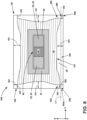
- FIG. 8 depicts a top-down or plan view illustrating an example of a non-limiting aspect of a single semiconductor device cell 150 in accordance with a non-limiting aspect.
- the semiconductor device cell 150 can be configured to enable a reduced ON-state resistance Rds(on) of the MOSFET device 10 compared to conventional techniques.
- Rds(on) the ON-state resistance of the MOSFET device 10
- FIG. 8 depicts a semiconductor device cell 150 having a square geometry, other aspects are not so limited.
- the device cells 150 can have any other desired geometry or shape including, without limitation, elongated rectangular, hexagonal, polygonal, rounded, curved, varying width, elongated or distorted shapes, and various combinations thereof.
- the semiconductor device cell 150 can be disposed at the first surface 4 of a semiconductor layer 2 (e.g., a silicon carbide (SiC) semiconductor layer).
- the semiconductor device cell 150 can include a drift region 16 having the first conductivity type (as illustrated in FIG 1 ).
- the semiconductor device cell 150 can have a cell periphery 155 or boundary, and a center region 65.
- the cell periphery 155 can define a set of cell corners 69.
- the set of cell corners 69 can include a first cell corner 69a and a second cell corner 69b.
- the semiconductor device cell 150 can further include the body contact region 44, the source contact region 42, the source region 20, the channel region 28, the well region 18, and the JFET region 29. It may be appreciated that the semiconductor layer 2, the source region 20, including the source contact region 42, and the JFET region 29 can have a first conductivity type (e.g., n-type), while well region 18, including the body contact region 44 and the channel region 28 can have a second conductivity type (e.g., p-type).
- first conductivity type e.g., n-type
- well region 18, including the body contact region 44 and the channel region 28 can have a second conductivity type (e.g., p-type).
- the body contact region 44 can be disposed in the center region 65 that, as illustrated in FIG. 1 , can be part of the well region 18.
- the body contact region 44 can be surrounded by the source region 20 of the first conductivity type (e.g., an n-type. or a p-type).
- a periphery of the source region 20 can be surrounded by well region 18, which can in turn be surrounded by the channel region 28 of the second conductivity type. It may be appreciated that, in some aspects, portions of the source region 20 disposed below the source contact 22 can serve as portions of the source contact region 42 of the semiconductor device cell 150.
- the body contact region 44 of the semiconductor device cell 150 may be surrounded by the source contact region 42 of the source region 20, wherein the doping of the source contact region 42 may be the same as the remainder of the source region 20.
- the channel region 28 can be, in turn, surrounded by the JFET region 29.
- the JFET region 29 can be arranged about the cell periphery155 of the semiconductor device cell 150.
- the JFET region 29 can be adjacent the channel region 28 at the cell periphery 155.
- the JFET region 29 can include a set of corners disposed at and defining the cell corners 69.
- the JFET region 29 can include a first corner region 29a and a second corner region 29b.
- the JFET region 29 can define the cell periphery 155, or the cell corners 69, or both.
- At least a portion of the JFET region 29 can define a longitudinal axis L1 along a length or side of the periphery 155.
- the JFET region 29 along the length or side of the periphery 155 includes a first corner region 29a and an opposing second corner region 29b separated by a JFET intermediate region 29c.
- the channel region 28 can define one or more corners 28a, 28b.
- the corners 28a, 28b can define a right angle.
- each of the corners 28a, 28b can be proximal to a corresponding JFET corner region 29a, 29b.
- a respective first corner 28a of the channel region 28 can be proximal to the JFET region first corner region 29a, and a second corner 28b of the channel region 28 can be proximal to the JFET region second corner region 29b.
- the JFET intermediate region 29c can define a first width W1.
- the first width W1 can extend across the JFET intermediate region 29c orthogonal to the longitudinal axis L1.
- the first width W1 can extend from an edge of the JFET intermediate region 29c abutting a periphery 128 of the channel region 28 to the cell periphery 155.
- At least one of the first corner region 29a and second corner region 29b can define a second width W2.
- the second width W2 can extend across the JFET region 29 orthogonal to the longitudinal axis L1.
- the second width W2 can extend from an edge of one of the first corner region 29a or second corner region 29b of the JFET region 29 abutting the periphery 128 of the channel region 28 to the cell periphery 155.
- the first width W1 is greater than the second width W2.
- the first width W1 can be about 0.7 microns, and the second width W2 can be about 0.25 microns.
- the first width W1 can be within a range of 0.3 - 1.2 microns, and the second width W2 can be within a range of 0.07- 0.4 microns.
- the first width W1 can be at least 20% wider that the second width W2.
- first width W1 and second width W2 can vary as desired for various applications without departing from the scope of the disclosure herein. Regardless of the dimensions, or relative dimensions with respect to each other, or both, of the first width W1 and second width W2 are arranged or defined with the particular purpose of decreasing the ON-state resistance contribution of the JFET region 29, while maintaining robustness to breakdown voltages between the corners of neighboring semiconductor device cells 150, as illustrated in FIG. 9 .
- FIG. 9 depicts a top-down or plan view illustrating a system 170 (e.g., a cellular semiconductor device 160 such as a MOSFET) comprising a cellular array of square semiconductor device cells 150 in accordance with a non-limiting aspect.
- the non-limiting aspect of FIG. 9 is similar to the aspect depicted in FIG. 8 , with one difference being that FIG. 9 comprises a set of semiconductor device cells 150 arranged in an aligned cellular type layout.
- two semiconductor device cells 150 may be referred to as neighboring cells or adjacent cells when any portion of the boundaries of the two cells abut or touch (e.g., along a portion of the cell periphery 155 or at a corner 69, or both, of the semiconductor device cells 150).
- each square semiconductor device cell 150 of FIG. 9 can have eight neighboring or adjacent semiconductor device cells 150.
- the set of semiconductor device cells 150 can include a first, a second, a third and a fourth adjacent cell 151, 152, 153, 155 and second adjacent cell 152. It should be appreciated that while the illustrated example of FIG. 9 depicts a set of semiconductor device cells 150 having a rectangular or square geometry, other aspects are not so limited. In other non-limiting aspects, the semiconductor device cells 150 can have any other desired geometry or shape including, without limitation elongated rectangular, hexagonal, rounded, curved, varying width, elongated or distorted shapes, and various combinations thereof. As described in more detail herein, the semiconductor device cells 150 can be configured to enable a reduced ON-state resistance Rds(on) of the semiconductor device 160. Each semiconductor device cell 150 can be disposed at the first surface 4 of a semiconductor layer 2 (e.g., a silicon carbide (SiC) semiconductor layer).
- a semiconductor layer 2 e.g., a silicon carbide (SiC) semiconductor layer
- the JFET region 29 can be arranged about the cell periphery 155 of each respective semiconductor device cell 150.
- the first and second corner regions 29a, 29b of the JFET region 29 can be defined at the cell periphery 155 and can define the corners 69 for each semiconductor device cell 150.
- At least a portion of the JFET region 29 about the cell periphery 155 of at least one of the adjacent semiconductor device cells 150, (e.g., the first adjacent cell 151) can define the longitudinal axis L1 and have the first corner region 29a and opposing second corner region 29b separated by the JFET intermediate region 29c.
- a respective first corner 28a of the channel region 28 of the first adjacent cell can be proximal to the JFET first corner region 29a, and a second corner 28b of the channel region 28 can be proximal to the JFET second corner region 29b.
- the JFET region 29 of two adjacent semiconductor device cells 150 can abut along a portion of the cell periphery 155 of the first and second adjacent cells 151, 152. In this way, the abutting JFET regions 29 of the first adjacent cell 151 and the second adjacent cell 152, can define a shared JFET region 29d.
- the abutting JFET regions 29 (i.e., the shared JFET region 29d) can define a third width W3.
- the third width W3 can extend across abutting JFET intermediate regions 29c of the first and second adjacent cells 151, 152, orthogonal to the longitudinal axis L1.
- the third width W3 can extend from edge of the periphery of the JFET intermediate region 29c abutting the channel region 28 of the first adjacent cell 151, across the abutting JFET regions 29 of the first and second adjacent cells 151, 152 to the periphery 128 of the channel region 28 of the second adjacent cell 152.
- the third width W3 can be defined as the shortest distance across the JFET region 29 of the first adjacent cell 151 and JFET region 29 of the second adjacent cell 152, between regions (e.g., channel regions 28) having the opposite doping type (e.g., p -type) compared that of the JFET region 29 (e.g., n-type).
- the abutting JFET regions 29 can define a fourth width W4.
- the fourth width W4 can extend across the JFET regions 29 of the first and second adjacent cells 151, 152, orthogonal to the longitudinal axis L 1 and proximal to at least one of the first corner region 29a and second corner regions 29b of the first and second adjacent cells 151, 152.
- the fourth width W4 can extend from an edge of the periphery of the channel region 28 (e.g., at a respective first or second corner 28a, 28b) of a particular first adjacent cell 151, across the JFET region to the periphery of the channel region 28 of a second adjacent cell 152 (e.g., at a corresponding first or second corner 28a, 28b).
- the fourth width W4 can extend from an edge of one of the first corner region 29a or second corner region 29b of the JFET region 29 abutting the periphery of the channel region 28 of the first adjacent cell 151, across the JFET regions 29 of the first and second adjacent cells 151, 152, to the periphery of the channel region 28 of the second adjacent cell 152.
- the fourth width W4 can be defined as the shortest distance across the JFET region 29 of the first adjacent cell 151 and JFET region 29 of the second adjacent cell 152, from a corner 28a, 28b of the channel region 28 of the first adjacent cell 151 having the opposite doping type (e.g., p -type) compared that of JFET region 29 (e.g., n-type) to a corner 28a, 28b of the channel region 28of the second adjacent cell 152 having the opposite doping type ( e.g., p -type) compared that of JFET region 29 (e.g., n-type).
- the opposite doping type e.g., p -type
- the third width W3 can be equal to a sum of a respective first width W1 of the first adjacent cell and the first width W1 of the second adjacent cell 152.
- the fourth width W4 can equal to a sum of respective second width W2 of the first adjacent cell and the second width W2 of the second adjacent cell 152.
- the fourth width W4 defined by the first and second adjacent cells 151, 152 can be greater than the third width W3 defined by the first and second adjacent cells 151, 152.
- the third width W3 can be about 1.3 microns, and the fourth width W4 can be about 0.45 microns. In other aspects, the third width W3 can be within a range of 0.5-2.2 microns, and the fourth width W4 can be within a range of 0.2-0.9 microns. In still other aspects, the third width W3 can be at least 20% wider than the fourth width W4.
- the dimensions of the third width W3, or the fourth width W4, or both can vary as desired for various applications without departing from the scope of the disclosure herein. Regardless of the dimensions, or relative dimensions with respect to each other, or both, of the third width W3 and fourth width W4 are arranged or defined with the particular purpose of decreasing the ON-state resistance contribution of the respective JFET regions 29 of the set of semiconductor device cells 150, while maintaining robustness to breakdown voltages between the corners of neighboring device cells 150.
- the disclosed aspects provide for a reduction in ON state resistance of semiconductor device cells 150 over conventional techniques by increasing a width of the JFET region 29 at the cell periphery 155, away from the first and second corner regions 29a, 29b without modifying (e.g., reducing or increasing) the dimensions of the channel region corners 28a, 28b proximal to the respective corners 69 of the cell, thereby avoiding or reducing an increase in the of electric field at the respective corners 69 of the cell which may result in improved long-term reliability for these semiconductor device cells 150.
- the presently disclosed semiconductor device cell 150 reduces device conduction losses (e.g., minimizes the ON-state resistance Rds(on)) by providing increased width of portions of the JFET region without decreasing the distance between the channel regions 28 at the corners 69 of adjacent semiconductor device cells 150.
- a system (160) comprising: a semiconductor device cell (150) comprising a semiconductor layer (2) including a drift region (16) having a first conductivity type; a well region (18) having a second conductivity type disposed adjacent to the drift region (16); a source region (20) having the first conductivity type disposed adjacent to and surrounded by the well region (18); a channel region (28) having the second conductivity type, disposed around and adjacent to the well region (18); and a JFET region (29) abutting a periphery of the channel region (128) and defining a semiconductor cell periphery (155) the JFET region having at least a first corner (69a), a second corner (69b), separated by a JFET intermediate region (29c), wherein a first width W1 of the JFET intermediate region (29c) extending from an edge of the JFET intermediate region (29c) abutting the periphery of the channel region (128) to the semiconductor cell periphery (155) is greater than a second width W2 of
- each of the first corner region (269a) and the second corner region (29b) define a right angle.
- channel region (28) defines a third corner region (28a) proximal to the first corner region 29a.
- channel region (28) defines a fourth corner region (28b), proximal the second corner region (29b).
- JFET region (29) extends from the channel region (28) to the semiconductor cell periphery (155).
- each device cell respectively comprises: semiconductor layer (2) including a drift region (16) having a first conductivity type; a well region (18) having a second conductivity type disposed adjacent to the drift region (16); a source region (20) having the first conductivity type disposed adjacent to and surrounded by the well region (18); a channel region (28) having the second conductivity type, disposed around and adjacent to the well region (18); and a JFET region (29) abutting a periphery of the channel region (128) and defining a semiconductor cell periphery (155) the JFET region having at least a first corner (69a), a second corner (69b), separated by a JFET intermediate region (29c), wherein a first width W1 of the JFET intermediate region (29c) extending from an edge of the JFET intermediate region (29
- each semiconductor device cell (150) comprises a respective semiconductor cell periphery (155) aligned with a respective semiconductor cell periphery (155) of an adjacent semiconductor device cell (150).
- a third width (W3) of the shared JFET region is greater than a fourth width (W4) between the respective channel regions (28) of the first semiconductor device cell (151) and the second semiconductor device cell (152) at at least one of the respective first corner region (29a) and the second corner region (29b).
- the third width W3 is equal to a sum of a respective first width (W1) the first semiconductor device 151 and a respective first width (W1) of the second semiconductor device cell 152.
- the fourth width (W4) is equal to a sum of a respective second width (W2) the first semiconductor device cell (151) and a respective second width (W2) of the second semiconductor device cell (152).
- a semiconductor device cell (150) comprising: a semiconductor layer (2) including a drift region(16) having a first conductivity type; a well region (18) having a second conductivity type disposed adjacent to the drift region (16); a source region (20) having the first conductivity type disposed adjacent to and surrounded by the well region (18); a channel region (28) having the second conductivity type, disposed around and adjacent to the well region (18); and a JFET region (29) abutting a periphery of the channel region (128) and defining a semiconductor cell periphery (155) the JFET region having at least a first corner (69a),a second corner (69b), and a JFET intermediate region (29c) having a first end disposed (29a) proximal the first corner (69a) and an opposing second end (29b) proximal the second corner (69b), wherein a first width W1 of the JFET intermediate region (29c) extending from an edge of the JFET intermediate region (29c)
- each of the first corner region (29a) and second corner region (29b) define a right angle.
- a system (160) comprising: a set of semiconductor device cells (150) at least partially disposed in a semiconductor layer (2) having a first conductivity type, wherein each device cell (150) respectively comprises: a semiconductor layer (2) including a drift region (16) having a first conductivity type; a well region (18) having a second conductivity type disposed adjacent to the drift region; a source region (20) having the first conductivity type disposed adjacent to and surrounded by the well region (18); a channel region (28) having the second conductivity type, disposed around and adjacent to the well region (18), the channel region (28); and a JFET region (29) abutting a periphery (128) of the channel region (28) and defining a semiconductor cell periphery (155) and having at least a first corner (69a),a second corner(69b), and a JFET intermediate region (29c) having a first end disposed (29a) proximal the first corner (69a) and an opposing second end (29b) proximal the second corner
- each semiconductor device cell (150) comprises a respective semiconductor cell periphery (155) aligned with a respective semiconductor cell periphery (155) of an adjacent semiconductor device cell (150).
- a third width (W3) of the shared JFET region (29d) is greater than a fourth width (W4) between the respective channel regions (28) of the first semiconductor device cell (151) and the second semiconductor device cell (152) at at least one of the first corner region (29a) and the second corner region (29b).
- the third width W3 is equal to a sum of a respective first width (W1) of the first semiconductor device 151 and a respective first width (W1) of the second semiconductor device cell 152.
- the fourth width (W4) is equal to a sum of a respective second width (W2) the first semiconductor device cell (151) and a respective second width (W2) of the second semiconductor device cell (152).
Landscapes
- Insulated Gate Type Field-Effect Transistor (AREA)
- Electrodes Of Semiconductors (AREA)
- Junction Field-Effect Transistors (AREA)
Abstract
A semiconductor device cell (150) includes a JFET region (29) adjacent a channel region (28) and defines a periphery of the semiconductor device cell (150). The JFET region (29) includes a JFET segment (29c) having a first end (29a) disposed proximal a first corner (69a) of the semiconductor device cell (150) and an opposing second end (29b) proximal a second corner (69b) of the semiconductor device cell (150). The JFET segment (29c) has a first width (W1) between the first end (29a) and the second end (29b) that is greater than a second width (W2) of the JFET region (29) the first end (29a) and the second end (29b).
Description
- This disclosure generally relates to semiconductor power devices, such as silicon carbide power devices, and more particularly to a semiconductor device cell having a layout that enables improved semiconductor device performance.
- Semiconductor devices, such as silicon carbide (SiC) power devices, are widely used in conventional electrical systems to switch or convert electrical power for consumption by a load. Many electronics systems utilize various semiconductor devices and components, such as thyristors, diodes, and various types of transistors (e.g., metal-oxide-semiconductor field-effect transistor (MOSFETs), insulated gate bipolar transistors (IGBTs), and other suitable transistors). For example, MOSFETs can be fabricated as discrete transistor packages for high power applications, or as chips with millions of transistors. Many thousands of these transistor "cells" can be combined into one device in order to handle relatively high currents and voltages.
- Many conventional MOSFETs use a vertical structure with source and drain terminals at opposite sides of a chip. The vertical orientation eliminates crowding at the gate and offers larger channel widths. Generally, when a semiconductor device is conducting current, the on-state resistance of the device represents its conduction loss, which impacts the efficiency of the device and its cost. That is, conventional semiconductor device cells include a number of internal components that can create resistance to the current flowing through the device.
- In the drawings:
-
FIG. 1 is a schematic of a typical planar MOSFET device. -
FIG. 2 is a schematic illustrating resistance for various regions of a typical MOSFET device. -
FIG. 3 is a chart depicting the relative resistance contributions of the regions of the MOSFET device structure ofFIG. 2 . -
FIG. 4 is a top-down view of a surface of a SiC layer that includes a typical MOSFET device structure having a stripe cell layout. -
FIG. 5 is a top-down view of a surface of a SiC layer that includes a typical MOSFET device structure having a stripe cell layout. -
FIG. 6 is a top-down view of a surface of a SiC layer that includes a typical MOSFET device structure having a cellular layout. -
FIG. 7 is a graph depicting normalized electric field strength in a portion of a SiC layer and in a portion of a dielectric layer disposed over the SiC layer, wherein the portion of the SiC layer is disposed between the corners of the well regions of conventional square device cells under reverse bias. -
FIG. 8 is a top-down view of a single semiconductor device cell in accordance with various aspects described herein. -
FIG. 9 is a top-down view of a system comprising a cellular array of semiconductor device cells in accordance with various aspects described herein. - Aspects of the disclosure can be implemented in any environment, apparatus, or method for cooling a heat-generating module regardless of the function performed by the heat-generating module.
- As used herein, the term "set" or a "set" of elements can be any number of elements, including only one. When introducing elements of various embodiments of the present disclosure, the articles "a," "an," and "the" are intended to mean that there are one or more of the elements. The terms "comprising," "including," and "having" are intended to be inclusive and mean that there may be additional elements other than the listed elements. Additionally, it should be understood that references to "one aspect" or "an aspect" of the present disclosure are not intended to be interpreted as excluding the existence of additional aspects that also incorporate the recited features.
- It may be appreciated that the shapes, positions, and alignments of features presently disclosed are, for the sake of simplicity, illustrated and described as being relatively ideal (e.g., square, rectangular, and hexagonal cells and shielding regions with perfectly straight and aligned features). However, as may be appreciated by one of skill in the art, process variations and technical limitations may result in cellular designs with less than ideal shapes or irregular features may still be in accordance with the present disclosure. As such, the term "substantially" as used herein to describe a shape, a position, or an alignment of a feature is meant to encompass ideal or target shapes, positions, and alignments as well as imperfectly implemented shapes, positions, and alignments resulting from variability in the semiconductor fabrication process, as may be appreciated by one skilled in the art.
- Additionally, semiconductor device cells are described herein as being disposed or fabricated "at the surface," "in the surface," "on the surface," or "along the surface" of a semiconductor layer, which is intended to include semiconductor device cells having portions disposed within the bulk of the semiconductor layer, portions disposed proximate to the surface of the semiconducting layer, portions disposed even with the surface of the semiconductor layer, and/or portions disposed above or on top of the surface of the semiconductor layer.
- While terms such as "voltage", "current", and "power" can be used herein, it will be evident to one skilled in the art that these terms can be interrelated when describing aspects of the electrical circuit, or circuit operations.
- All directional references (e.g., radial, axial, upper, lower, upward, downward, left, right, lateral, front, back, top, bottom, above, below, vertical, horizontal, clockwise, counterclockwise) are used for identification purposes to aid the reader's understanding of the disclosure, and do not create limitations, particularly as to the position, orientation, or use thereof. Connection references (e.g., attached, coupled, connected, and joined) are to be construed broadly and can include intermediate members between a collection of elements and relative movement between elements unless otherwise indicated. As such, connection references do not necessarily infer that two elements are directly connected and in fixed relation to each other. In non-limiting examples, connections or disconnections can be selectively configured to provide, enable, disable, or the like, an electrical connection between respective elements. The exemplary drawings are for purposes of illustration only and the dimensions, positions, order and relative sizes reflected in the drawings attached hereto can vary.
- As used herein, a controllable switching element, or a "switch" is an electrical device that can be controllable to toggle between a first mode of operation, wherein the switch is very low resistance state or in an "ON" state, or otherwise in a conducting mode, intending to transmit current from a switch input to a switch output, and a second mode of operation, wherein the switch is very high resistance state or in an OFF state, or otherwise in a non-conducting mode, intending to prevent current from transmitting between the switch input and switch output. In non-limiting examples, connections or disconnections, such as connections enabled or disabled by the controllable switching element, can be selectively configured to provide, enable, disable, or the like, an electrical connection between respective elements.
- Furthermore, for ease of description and understanding, while various aspects may be discussed below in the context of SiC MOSFET devices, it should be appreciated the present approach may be applicable to other types of MOSFETS, such as, but not limited to SiC DMOSFETs, UMOSFETs, and VMOSFETs. It is contemplated that various material systems (e.g., silicon (Si), germanium (Ge), aluminum nitride (AlN), gallium nitride (GaN), gallium arsenide (GaAs), diamond (C), or any other suitable wide band-gap semiconductor) can be used. It is further contemplated that other types of device structures (e.g., UMOSFET, VMOSFETs, insulated gate bipolar transistors (IGBT), insulated base MOS-controlled thyristors (IBMCT), or any other suitable FET and/or MOS device)) utilizing n-channel or p-channel designs can be used in various non-limiting aspects.
- One of the most common solid-state semiconductor switching devices used in modern power electronics is the MOSFET device. While an ideal switch would conduct electrical current with zero electrical resistance when in a low resistance "ON" or conducting state, a MOSFET will always exhibit a finite electrical resistance. Thus, it is generally desirable to reduce the total resistance (e.g., an on-state resistance) to the minimum possible value. It is also desirable to minimize the ON-state resistance of the MOSFET, without reducing the OFF-state resistance, the switching speed of the device, or both.
- Conventional MOSFETs typically consist of arrays of periodic unit cells. Each unit cell can have a respective electrical resistance, and the MOSFET on-state electrical resistance can be defined by the sum of the respective cell resistances in a parallel electrical circuit. Additionally, each unit cell resistance can be defined by a set of respective resistance values of the structural components of the cell coupled in series. The on-state resistance of a particular MOSFET can thus be defined based at least in part on the relative geometric structures of the various functional components within the respective cells.
- When a MOSFET is in a conducting or ON-state, electrons flow through each individual cell from a "source metal" on the top surface of a SiC semiconductor body, through various structures defined within the SiC semiconductor body, and into a "drain metal" on the back surface of the body. Each respective MOSFET unit cell surface can include four mutually exclusive, non-overlapping regions referred to herein as the source contact region, the n+/p-well region, the channel /accumulation ("channel") region, and the junction field-effect transistor ("JFET") region. The four regions can be coupled electrically in series, and can occupy substantially the entire area of the respective cell.
- The resistive contributions of the source contact and the channel regions to the on-state electrical resistance of the MOSFET are inversely proportional to their respective areas. The resistive contribution of the n+/p-well region to the on-state electrical resistance of the MOSFET is roughly directly proportional to its area. Since the resistive contribution of the channel region is relatively greater than that of the n+/p-well, or the source contact region, the on-state electrical resistance of the MOSFET can be reduced by maximizing the relative area of the channel region in the unit cell with respect to the n+/p-well, or the source contact region. Thus, conventional techniques typically employ MOSFET structures with a maximized relative proportion of the channel region area by arranging the cell geometries to minimize the relative proportion of the n+/p-well region area, or the source contact region area, or both, with respect to the channel region, JFET region or both.
- However, for SiC MOSFETs, current fabrication technology can limit such optimization. For example, conventional techniques have focused on reducing MOSFET on-state resistance using periodic cells produced by surrounding a minimum size source contact region with a minimum size n+ region, relative to the channel region. However, the minimum fabricable source contact region dimensions (using conventional fabrication techniques) can be larger than a calculated or determined optimized area. Additionally, enlarging the channel region of adj acent cells can result in off-state breakdown voltage degradation at the cell corners.
- Accordingly, as described in more detail herein, in non-limiting aspects, the cells can be arranged to increase the relative proportion of the JFET region between adjacent aligned cells, while maintaining the relative geometry of channel region with respect to the JFET region at the cell corners. In this way, aspects as described herein can thereby arrange a greater net relative proportion of the JFET region area with respect to the source contact region or size n+ region, or both, compared to conventional techniques, and thereby achieve an improved (i.e., lower) on-state resistance for the respective cell than conventional devices. Furthermore, by maintaining the geometry of channel region with respect to the JFET region at the cell corners, while enlarging the JFET region between the corners can avoid the off-state breakdown voltage degradation at the cell corners of some prior art solutions.
- As will be described in more detail herein, an undesirable increase in on-state resistance resulting from the increased area of the n+/p-well region (e.g., in the alternating bands), can be negated or overcome within a predetermined dimensional range, due to the decrease in on-state resistance achieved by the corresponding increased area of the JFET region, thereby resulting in a net decrease in the on-state resistance of the respective cell compared to conventional designs.
-
FIG. 1 illustrates an active cell of a conventional planar n-channel field-effect transistor, such as a DMOSFET, hereinafterMOSFET device 10. It may be appreciated that, in order to more clearly illustrate and describe certain components of theMOSFET device 10, as well as other devices discussed hereinbelow, certain commonly understood design elements (e.g., top metallization, passivation, edge termination, and so forth) may be omitted. - The illustrated
conventional MOSFET device 10 ofFIG. 1 includes a semiconductor layer 2 (e.g., an epitaxial SiC semiconductor layer) having afirst surface 4 and asecond surface 6. Thesemiconductor layer 2 includes adrift region 16 having a first conductivity type (e.g., an n-type drift region 16), awell region 18 having a second conductivity type (e.g., a p-well region 18) disposed adjacent to thedrift region 16 and proximal to thefirst surface 4. Thesemiconductor layer 2 also includes asource region 20 having the first conductivity type (e.g., an n-type source region 20) adjacent to thewell region 18 and proximal to thefirst surface 4. - A
source contact 22 is disposed on top of thefirst surface 4, partially coveringsource region 20 andwell region 18. - A dielectric layer 24 (also referred to as a gate insulating layer or gate dielectric layer) is disposed on a portion of the
first surface 4 of thesemiconductor layer 2, and agate electrode 26 is disposed on thedielectric layer 24. - The
second surface 6 of thesemiconductor layer 2 is a substrate layer 14 (e.g., a SiC substrate layer), and thedrain contact 12 is disposed on the bottom of theMOSFET device 10 along thesubstrate layer 14. - During on-state operation, an appropriate gate voltage (e.g., at or beyond a threshold voltage (VTH) of the MOSFET device 10) can cause an inversion layer to be formed in a
channel region 28, as well as a conductive path to be enhanced in a junction field-effect transistor (JFET)region 29 due to accumulation of carriers, allowing current to flow from the drain contact 12 (i.e., the drain electrode) to the source contact 22 (i.e., the source electrode). It should be appreciated that, for the MOSFET devices discussed herein, thechannel region 28 may be generally defined as an upper portion of thewell region 18 disposed below thegate electrode 26 and thedielectric layer 24. -
FIG. 2 is a schematic cross-sectional view of theconventional MOSFET device 10 ofFIG. 1 . Thesource contacts 22 of theMOSFET device 10 illustrated inFIG. 2 generally provide an ohmic connection to the source electrode, and are disposed over both a portion of thesource regions 20 and a portion of thewell regions 18. Thesource contact 22 is generally a metallic interface comprising one or more metal layers situated between these semiconductor portions of theMOSFET device 10 and the metallic source electrode. - For clarity, the portion of the source region 20 (e.g., an n+ source region 20) of the
MOSFET device 10 disposed below thesource contact 22 may be more specifically referred to herein as asource contact region 42 of theMOSFET device 10. Similarly, a portion of the well region 18 (e.g., a p-well region 18) of theMOSFET device 10, which may be p+ doped at a higher level than the remainder of thewell region 18, may be more specifically referred to herein as a body region 44 (e.g., p+ body region 44) of theMOSFET device 10. For clarity, the portion of thebody region 44 that is disposed below (e.g., covered by, directly electrically connected to) thesource contact 22, may be more specifically referred to herein as the body contact region 44 (e.g., p+ body contact region 44) of theMOSFET device 10. - For consistency, portions of the
source contact 22 may be designated herein based on the portion of the semiconductor device that is disposed below thesource contact 22. For example, the portion of thesource contact 22 disposed above thebody contact region 44 may be referred to herein as the body contact portion of thesource contact 22. Similarly, the portion of thesource contact 22 disposed above asource contact region 42 of theMOSFET device 10 may be referred to herein as a source contact portion of thesource contact 22. - As illustrated schematically in
FIG. 2 , the various regions of theMOSFET device 10 may each have an associated resistance, and a total resistance (e.g., an ON-state resistance, Rds(on)) of theMOSFET device 10, which may be represented as a sum of each of these resistances. For example, as illustrated inFIG. 2 , ON-state resistance, Rds(on), of theMOSFET device 10 may be approximated as a sum of: a source region resistance 30 (e.g., Rs, a resistance ofsource region 20 and a resistance of the source contact 22); an inversion channel resistance 32 (e.g., Rch, an resistance of thechannel region 28 illustrated inFIG. 2 ); an accumulation layer resistance 34 (e.g., Race, a resistance of an accumulation layer between thedielectric layer 24 and portion ofdrift region 16 located between well regions 18); a JFET region resistance 36 (e.g., RJFET, resistance of undepleted neck region between well regions 18); a drift region resistance 38 (e.g., Rdrift, the resistance about the drift region 16); and a substrate layer resistance 48 (e.g., Rsub, the resistance about the substrate layer 14). Note that the resistances illustrated inFIG. 2 are not intended to be exhaustive, and that other resistances (e.g., drain contact resistance, spreading resistance, etc.) could potentially be present within theMOSFET device 10. - In certain cases, one or two resistance components illustrated in
FIG. 2 may dominate conduction losses of theMOSFET device 10, and addressing these factors can significantly impact the ON-state resistance Rds(on). For example, for devices in which thedrift resistance 38, thesubstrate layer resistance 48 and the contact resistance are negligible, such as low-voltage devices or devices suffering from low inversion layer mobility (e.g., SiC devices), thechannel resistance 32 may account for a significant portion of device conduction losses. - By further example, in medium-voltage and high-voltage devices,
JFET region resistance 36 may account for a significant portion of total conduction losses. In some cases, the MOSFET channel and JFET can comprise approximately 55% of a typical semiconductor device on-state resistance. - With reference to
FIG. 3 , a chart depicting an example of the relative resistance contributions of the various regions of the MOSFET device structure ofFIG. 2 is illustrated. The relative resistance for each region is depicted as a function of the respective region distance (e.g., path length). It can be seen that theinversion channel resistance 32 of thechannel region 28 can be the largest contributor to the ON-state resistance Rds(on) of theMOSFET device 10, while the source region resistance 30 (e.g., a resistance ofsource region 20 and a resistance of the source contact 22), and substrate layer resistance 48 (e.g., the resistance about the substrate layer 14), contribute the least resistance to the ON-state resistance Rds(on) of theMOSFET device 10. -
FIG. 4 illustrates a top-down view of aconventional semiconductor layer 2 including a MOSFET device structure 41 having a conventional stripe cell layout. (i.e., a non-cellular layout). The illustrated stripe layout ofFIG. 4 includes: thechannel regions 28,source regions 20,source contact regions 42,body contact regions 44, andJFET region 29. It may be appreciated that a set ofsource contact regions 42 and a set ofbody contact regions 44 can be formed as continuous stripes along the surface of the semiconductor for the illustrated stripe layout ofFIG. 4 . - In terms of dimensions, the conventional MOSFET device structure 41 may be described as having the
channel region 28 having aparticular channel length 43, adistance 45 fromchannel region 28 to sourceregion 20, awidth 47 of the source andbody contact regions width 49 of theJFET region 29. While the conventional stripe cell layout illustrated inFIG. 4 offers good reliability (e.g., long term and high temperature performance), the relativelyhigh channel resistance 32 andJFET resistance 36 of the MOSFET device structure 41 results in a relatively high ON-state resistance Rds(on), which diminishes the electrical performance of the device.
An example of another conventional device layout is illustrated inFIG. 5 , which is a top-down or plan view of a stripe ladder device layout 40 (i.e., a non-cellular layout) with segmented source/body contacts. The illustrated stripeladder device layout 40 includes:channel regions 28,source regions 20, a set of segmented source/body contacts 46 (including thebody contact region 44 and the source contact region 42) andJFET region 29.FIG. 5 further illustrates dimensions of the stripeladder device layout 40, including: thechannel region 28 having achannel length 43, thedistance 45 from the channel to thesource region 20, thewidth 47 of the source andbody contact regions width 49 of theJFET region 29,segment length 51 of thesource contact region 42,segment length 52 of thebody contact region 44, subset ofdevice area 53, and awidth 55 of a JFET area 54 within subset of device area 53for the illustrated stripeladder device layout 40. - For further comparison, another example of a conventional device layout is illustrated in
FIG. 6 . It may be appreciated that the layouts illustrated herein using a few device cells that represent a subset of the numerous device cells of a semiconductor device on the surface of thesemiconductor layer 2. It may be further appreciated that forFIGS. 4-6 , as well as for the top-down views of device cells presented below, certain features of the device cells (e.g.,gate electrode 26,dielectric layer 24, source contact 22) can be omitted to provide an unobstructed view of the surface of thesemiconductor layer 2. In particular,FIG. 6 illustrates a set ofdevice cells 50 in an aligned layout, that is, where thedevice cells 50 are not staggered or offset from each other. - In general, the illustrated conventional cell design and layout illustrated in
FIG. 6 can enable reduced values of Rd (on) by reducing bothchannel resistance 32 and the JFET resistance relative to a conventional stripe cell layout, as illustrated inFIG. 5 . For example, thedevice cells 50 ofFIG. 6 provide an approximately 20% lower Rd (on) than the stripe MOSFET device structure 41 ofFIG. 5 assuming similar fabrication process-limited dimensions. - In
FIG. 6 , the illustratedconventional device cell 50 includes thebody contact region 44 disposed in thecenter region 65 of each cell that, as illustrated in FIG. 1B, can be part of thewell region 18. Thebody contact region 44 is surrounded by thesource region 20. More specifically, thebody contact region 44 of eachcell 50 may be surrounded by thesource contact region 42 of thesource region 20, wherein the doping of thesource contact region 42 may be the same as the remainder of thesource region 20. Thesource region 20 of eachcell 50 is surrounded by achannel region 28, which also is part of thewell region 18, as illustrated in FIG. l. Thechannel region 28 is, in turn, surrounded by theJFET region 29. - While the device layout illustrated in
FIG. 6 may enable lower ON-state resistance Rds(on) relative to a stripe cell layout, as illustrated inFIG. 5 , it is recognized that such designs can have a substantially higher electric field in portions of theJFET region 29 between the corners of thewell regions 18 of neighboringdevice cells 50 under blocking conditions. For SiC MOS devices, the electric field in the dielectric layer 24 (e.g., silicon dioxide (SiO2)) disposed over the JFET region 29 (illustrated inFIGS. 1 and2 ) can be around ten times higher compared to that in silicon devices when thedevice cells 50 operate under reverse bias. While SiC is generally robust toward higher electric fields, thedielectric layer 24 may experience breakdown during long term operation, resulting in reliability issues with thedevice cells 50. - In particular, in a SiC MOSFET under reverse bias, the electric field present in the widest portion of the
JFET region 29 between respectiveadjacent corners 28a of thechannel regions 28 of neighboringdevice cells 50, at thecorner 69 where neighboringdevice cells 50 meet (illustrated adistance 60, along thediagonal arrow 66 inFIGS. 6 ) is substantially higher than in other portions of theJFET region 29. Accordingly, it would be desirable to reduce the size of theJFET region 29 between thecorners 28a of thechannel regions 28 of neighboringdevice cells 50. -
FIG. 7 is agraph 70 that plots the strength of the electric field (in arbitrary units (au)) for portions of a conventionalSiC device cell 50 under reverse bias, wherein the portions are linearly disposed along thediagonal arrow 66 illustrated inFIG. 6 . Thegraph 70 ofFIG. 7 includes afirst curve 72 illustrating the electric field in thesemiconductor layer 2, and includes asecond curve 74 illustrating the electric field in thedielectric layer 24 disposed over the semiconductor layer 2 (shown in FIG. l). - As illustrated in
FIG. 7 , at the center of the conventional SiC device cell 50 (i.e., at x=0 µm) the electric field is low, and, moving diagonally through the corner of theconventional device cell 50, the electric field increases to a peak field strength in the middle of theJFET region 29. The peak or maximum electric field between cell corners (i.e.,distance 60, along thediagonal arrow 66 ofFIG. 6 ) is approximately 20% higher than the peak or maximum electric field would be between parallel portions of the device cells 50 (i.e.,width 49, along the arrow 64 ofFIG. 3 ). As a result, as shown inFIG. 7 , the peak electric field in thedielectric layer 24 is greater between the corners of thewell regions 18 of neighboring device cells 50 (e.g., between the corners of thechannel regions 28 of neighboringdevice cells 50, at thecorner 69 where neighboringdevice cells 50 meet), which may result in long term reliability issues for suchunshielded device cells 50. - With the foregoing in mind, present aspects are directed toward semiconductor device designs and layouts that enable improved semiconductor device performance. In particular, aspects as disclosed herein are configured to reduce the electric field in the JFET regions 29 (as well as in the
dielectric layer 24 illustrated inFIG. 1 ) in locations where thecorners 69 of neighboringdevice cells 50 meet without significantly increasing the ON-state resistance Rds (on) of thesemiconductor device cell 50. - Accordingly, the presently disclosed aspects are arranged having portions of the
JFET region 29 with an increased width relative to the portions of theJFET region 29 at thecell corners 69, so that the distance betweenchannel regions 28 at thecorners 69 of neighboringdevice cells 50 is less than the distance between parallel portions of thechannel regions 28 of the neighboringdevice cells 50. Therefore, the present aspects can ensure no portion of theJFET region 29 is wider than the width of theJFET region 29 between parallel portions of thechannel regions 28 of neighboringdevice cells 50. -
FIG. 8 , depicts a top-down or plan view illustrating an example of a non-limiting aspect of a singlesemiconductor device cell 150 in accordance with a non-limiting aspect. As described in more detail herein, thesemiconductor device cell 150 can be configured to enable a reduced ON-state resistance Rds(on) of theMOSFET device 10 compared to conventional techniques. It should be appreciated that while the illustrated example ofFIG. 8 depicts asemiconductor device cell 150 having a square geometry, other aspects are not so limited. In other non-limiting aspects, thedevice cells 150 can have any other desired geometry or shape including, without limitation, elongated rectangular, hexagonal, polygonal, rounded, curved, varying width, elongated or distorted shapes, and various combinations thereof. - The
semiconductor device cell 150 can be disposed at thefirst surface 4 of a semiconductor layer 2 (e.g., a silicon carbide (SiC) semiconductor layer). Thesemiconductor device cell 150 can include adrift region 16 having the first conductivity type (as illustrated inFIG 1 ). Thesemiconductor device cell 150 can have acell periphery 155 or boundary, and acenter region 65. In non-limiting aspects, thecell periphery 155 can define a set ofcell corners 69. For example, the set ofcell corners 69 can include a first cell corner 69a and asecond cell corner 69b. - The
semiconductor device cell 150 can further include thebody contact region 44, thesource contact region 42, thesource region 20, thechannel region 28, thewell region 18, and theJFET region 29. It may be appreciated that thesemiconductor layer 2, thesource region 20, including thesource contact region 42, and theJFET region 29 can have a first conductivity type (e.g., n-type), whilewell region 18, including thebody contact region 44 and thechannel region 28 can have a second conductivity type (e.g., p-type). - As illustrated in
FIG. 8 , thebody contact region 44 can be disposed in thecenter region 65 that, as illustrated inFIG. 1 , can be part of thewell region 18. Thebody contact region 44 can be surrounded by thesource region 20 of the first conductivity type (e.g., an n-type. or a p-type). A periphery of thesource region 20 can be surrounded bywell region 18, which can in turn be surrounded by thechannel region 28 of the second conductivity type. It may be appreciated that, in some aspects, portions of thesource region 20 disposed below thesource contact 22 can serve as portions of thesource contact region 42 of thesemiconductor device cell 150. More specifically, thebody contact region 44 of thesemiconductor device cell 150 may be surrounded by thesource contact region 42 of thesource region 20, wherein the doping of thesource contact region 42 may be the same as the remainder of thesource region 20. Thechannel region 28 can be, in turn, surrounded by theJFET region 29. - The
JFET region 29 can be arranged about the cell periphery155 of thesemiconductor device cell 150. TheJFET region 29 can be adjacent thechannel region 28 at thecell periphery 155. TheJFET region 29 can include a set of corners disposed at and defining thecell corners 69. For example, theJFET region 29 can include afirst corner region 29a and asecond corner region 29b. As such, theJFET region 29 can define thecell periphery 155, or thecell corners 69, or both. At least a portion of theJFET region 29 can define a longitudinal axis L1 along a length or side of theperiphery 155. TheJFET region 29 along the length or side of theperiphery 155 includes afirst corner region 29a and an opposingsecond corner region 29b separated by a JFETintermediate region 29c. - In non-limiting aspects, the
channel region 28 can define one ormore corners corners corners JFET corner region first corner 28a of thechannel region 28 can be proximal to the JFET regionfirst corner region 29a, and asecond corner 28b of thechannel region 28 can be proximal to the JFET regionsecond corner region 29b. - The JFET
intermediate region 29c can define a first width W1. The first width W1 can extend across the JFETintermediate region 29c orthogonal to the longitudinal axis L1. In aspects, the first width W1 can extend from an edge of the JFETintermediate region 29c abutting aperiphery 128 of thechannel region 28 to thecell periphery 155. - At least one of the
first corner region 29a andsecond corner region 29b can define a second width W2. The second width W2 can extend across theJFET region 29 orthogonal to the longitudinal axis L1. In aspects, the second width W2 can extend from an edge of one of thefirst corner region 29a orsecond corner region 29b of theJFET region 29 abutting theperiphery 128 of thechannel region 28 to thecell periphery 155. - In non-limiting aspects, the first width W1 is greater than the second width W2. In non-limiting aspects, the first width W1 can be about 0.7 microns, and the second width W2 can be about 0.25 microns. In other aspects, the first width W1 can be within a range of 0.3 - 1.2 microns, and the second width W2 can be within a range of 0.07- 0.4 microns. In still other aspects, the first width W1 can be at least 20% wider that the second width W2.
- Other aspects are not so limited, and the dimensions of the first width W1, or the second width W2, or both, can vary as desired for various applications without departing from the scope of the disclosure herein. Regardless of the dimensions, or relative dimensions with respect to each other, or both, of the first width W1 and second width W2 are arranged or defined with the particular purpose of decreasing the ON-state resistance contribution of the
JFET region 29, while maintaining robustness to breakdown voltages between the corners of neighboringsemiconductor device cells 150, as illustrated inFIG. 9 . -
FIG. 9 depicts a top-down or plan view illustrating a system 170 (e.g., acellular semiconductor device 160 such as a MOSFET) comprising a cellular array of squaresemiconductor device cells 150 in accordance with a non-limiting aspect. The non-limiting aspect ofFIG. 9 is similar to the aspect depicted inFIG. 8 , with one difference being thatFIG. 9 comprises a set ofsemiconductor device cells 150 arranged in an aligned cellular type layout. As used herein, twosemiconductor device cells 150 may be referred to as neighboring cells or adjacent cells when any portion of the boundaries of the two cells abut or touch (e.g., along a portion of thecell periphery 155 or at acorner 69, or both, of the semiconductor device cells 150). As such, it may be appreciated that, each squaresemiconductor device cell 150 ofFIG. 9 can have eight neighboring or adjacentsemiconductor device cells 150. - As illustrated in
FIG. 9 , the set ofsemiconductor device cells 150 can include a first, a second, a third and a fourthadjacent cell adjacent cell 152. It should be appreciated that while the illustrated example ofFIG. 9 depicts a set ofsemiconductor device cells 150 having a rectangular or square geometry, other aspects are not so limited. In other non-limiting aspects, thesemiconductor device cells 150 can have any other desired geometry or shape including, without limitation elongated rectangular, hexagonal, rounded, curved, varying width, elongated or distorted shapes, and various combinations thereof. As described in more detail herein, thesemiconductor device cells 150 can be configured to enable a reduced ON-state resistance Rds(on) of thesemiconductor device 160. Eachsemiconductor device cell 150 can be disposed at thefirst surface 4 of a semiconductor layer 2 (e.g., a silicon carbide (SiC) semiconductor layer). - As shown, the
JFET region 29 can be arranged about thecell periphery 155 of each respectivesemiconductor device cell 150. The first andsecond corner regions JFET region 29 can be defined at thecell periphery 155 and can define thecorners 69 for eachsemiconductor device cell 150. At least a portion of theJFET region 29 about thecell periphery 155 of at least one of the adjacentsemiconductor device cells 150, (e.g., the first adjacent cell 151) can define the longitudinal axis L1 and have thefirst corner region 29a and opposingsecond corner region 29b separated by the JFETintermediate region 29c. In non-limiting aspects, a respectivefirst corner 28a of thechannel region 28 of the first adjacent cell can be proximal to the JFETfirst corner region 29a, and asecond corner 28b of thechannel region 28 can be proximal to the JFETsecond corner region 29b. - When arranged as an aligned cellular array, the
JFET region 29 of two adjacentsemiconductor device cells 150, for example, the firstadjacent cell 151 and the secondadjacent cell 152, can abut along a portion of thecell periphery 155 of the first and secondadjacent cells JFET regions 29 of the firstadjacent cell 151 and the secondadjacent cell 152, can define a sharedJFET region 29d. - The abutting JFET regions 29 (i.e., the shared
JFET region 29d) can define a third width W3. The third width W3 can extend across abutting JFETintermediate regions 29c of the first and secondadjacent cells intermediate region 29c abutting thechannel region 28 of the firstadjacent cell 151, across the abuttingJFET regions 29 of the first and secondadjacent cells periphery 128 of thechannel region 28 of the secondadjacent cell 152. In general, the third width W3 can be defined as the shortest distance across theJFET region 29 of the firstadjacent cell 151 andJFET region 29 of the secondadjacent cell 152, between regions (e.g., channel regions 28) having the opposite doping type (e.g., p -type) compared that of the JFET region 29 (e.g., n-type). - The abutting
JFET regions 29 can define a fourth width W4. The fourth width W4 can extend across theJFET regions 29 of the first and secondadjacent cells first corner region 29a andsecond corner regions 29b of the first and secondadjacent cells second corner adjacent cell 151, across the JFET region to the periphery of thechannel region 28 of a second adjacent cell 152 (e.g., at a corresponding first orsecond corner first corner region 29a orsecond corner region 29b of theJFET region 29 abutting the periphery of thechannel region 28 of the firstadjacent cell 151, across theJFET regions 29 of the first and secondadjacent cells channel region 28 of the secondadjacent cell 152. In general, the fourth width W4 can be defined as the shortest distance across theJFET region 29 of the firstadjacent cell 151 andJFET region 29 of the secondadjacent cell 152, from acorner channel region 28 of the firstadjacent cell 151 having the opposite doping type (e.g., p -type) compared that of JFET region 29 (e.g., n-type) to acorner adjacent cell 152 having the opposite doping type ( e.g., p -type) compared that of JFET region 29 (e.g., n-type). - In non-limiting aspects, the third width W3 can be equal to a sum of a respective first width W1 of the first adjacent cell and the first width W1 of the second
adjacent cell 152. Similarly, in non-limiting aspects, the fourth width W4 can equal to a sum of respective second width W2 of the first adjacent cell and the second width W2 of the secondadjacent cell 152. In non-limiting aspects, the fourth width W4 defined by the first and secondadjacent cells adjacent cells - In non-limiting aspects, the third width W3 can be about 1.3 microns, and the fourth width W4 can be about 0.45 microns. In other aspects, the third width W3 can be within a range of 0.5-2.2 microns, and the fourth width W4 can be within a range of 0.2-0.9 microns. In still other aspects, the third width W3 can be at least 20% wider than the fourth width W4.
- Other aspects are not so limited, and the dimensions of the third width W3, or the fourth width W4, or both, can vary as desired for various applications without departing from the scope of the disclosure herein. Regardless of the dimensions, or relative dimensions with respect to each other, or both, of the third width W3 and fourth width W4 are arranged or defined with the particular purpose of decreasing the ON-state resistance contribution of the
respective JFET regions 29 of the set ofsemiconductor device cells 150, while maintaining robustness to breakdown voltages between the corners of neighboringdevice cells 150. - It may be appreciated that the disclosed aspects provide for a reduction in ON state resistance of
semiconductor device cells 150 over conventional techniques by increasing a width of theJFET region 29 at thecell periphery 155, away from the first andsecond corner regions channel region corners respective corners 69 of the cell, thereby avoiding or reducing an increase in the of electric field at therespective corners 69 of the cell which may result in improved long-term reliability for thesesemiconductor device cells 150. - Thus, the presently disclosed
semiconductor device cell 150 reduces device conduction losses (e.g., minimizes the ON-state resistance Rds(on)) by providing increased width of portions of the JFET region without decreasing the distance between thechannel regions 28 at thecorners 69 of adjacentsemiconductor device cells 150. - To the extent not already described, the different features and structures of the various aspects can be used in combination with each other as desired. That one feature cannot be illustrated in all of the aspects is not meant to be construed that it cannot be, but is done for brevity of description. Thus, the various features of the different aspects can be mixed and matched as desired to form new aspects, whether or not the new aspects are expressly described. Combinations or permutations of features described herein are covered by this disclosure.
- This written description uses examples to disclose aspects of the disclosure, including the best mode, and also to enable any person skilled in the art to practice aspects of the disclosure, including making and using any devices or systems and performing any incorporated methods. The patentable scope of the disclosure is defined by the claims, and can include other examples that occur to those skilled in the art. Such other examples are intended to be within the scope of the claims if they have structural elements that do not differ from the literal language of the claims, or if they include equivalent structural elements with insubstantial differences from the literal languages of the claims.
- The features disclosed in the foregoing description, in the following claims and/or in the accompanying drawings may, both separately and in any combination thereof, be material for realizing embodiments in diverse forms thereof.
- Various characteristics, aspects and advantages of the present disclosure may also be embodied in any permutation of aspects of the disclosure, including but not limited to the following technical solutions as defined in the enumerated aspects:
- A system (160) comprising: a semiconductor device cell (150) comprising a semiconductor layer (2) including a drift region (16) having a first conductivity type; a well region (18) having a second conductivity type disposed adjacent to the drift region (16); a source region (20) having the first conductivity type disposed adjacent to and surrounded by the well region (18); a channel region (28) having the second conductivity type, disposed around and adjacent to the well region (18); and a JFET region (29) abutting a periphery of the channel region (128) and defining a semiconductor cell periphery (155) the JFET region having at least a first corner (69a),a second corner (69b), separated by a JFET intermediate region (29c), wherein a first width W1 of the JFET intermediate region (29c) extending from an edge of the JFET intermediate region (29c) abutting the periphery of the channel region (128) to the semiconductor cell periphery (155) is greater than a second width W2 of the JFET region (29) extending from an edge of at least one of the first and second corner (69a), (69b) abutting the periphery of the channel region (128) to the semiconductor cell periphery (155).
- The system (160) of the preceding clause, wherein each of the first corner region (269a) and the second corner region (29b) define a right angle.
- The system (160) of any preceding clause, wherein the channel region (28) defines a third corner region (28a) proximal to the
first corner region 29a. - The system (160) of any preceding clause, wherein the channel region (28) defines a fourth corner region (28b), proximal the second corner region (29b).
- The system (160) of any preceding clause, wherein the JFET region (29) extends from the channel region (28) to the semiconductor cell periphery (155).
- The system (160) of any preceding clause, wherein the first width (W1) is within a range of 6 microns and 18 microns.
- The system (160) of any preceding clause, wherein the second width (W2) is within a range of 0.07 microns and 1.4 microns.
- The system (160) of any preceding clause, wherein the first width (W1) is at least 20% wider than the second width (W2).
- The system (160) of any preceding clause, wherein the semiconductor device cell (150) is a MOSFET device (10).
- The system (160) of any preceding clause, further comprising: a set of semiconductor device cells (151, 152, 153, 154) at least partially disposed in the semiconductor device layer (2) having the first conductivity type, wherein each device cell respectively comprises: semiconductor layer (2) including a drift region (16) having a first conductivity type; a well region (18) having a second conductivity type disposed adjacent to the drift region (16); a source region (20) having the first conductivity type disposed adjacent to and surrounded by the well region (18); a channel region (28) having the second conductivity type, disposed around and adjacent to the well region (18); and a JFET region (29) abutting a periphery of the channel region (128) and defining a semiconductor cell periphery (155) the JFET region having at least a first corner (69a),a second corner (69b), separated by a JFET intermediate region (29c), wherein a first width W1 of the JFET intermediate region (29c) extending from an edge of the JFET intermediate region (29c) abutting the periphery of the channel region (128) to the semiconductor cell periphery (155) is greater than a second width W2 of the JFET region (29) extending from an edge of at least one of the first and second corner (69a), (69b) abutting the periphery of the channel region (128) to the semiconductor cell periphery (155).
- The system (160) of any preceding clause, wherein each semiconductor device cell (150) comprises a respective semiconductor cell periphery (155) aligned with a respective semiconductor cell periphery (155) of an adjacent semiconductor device cell (150).
- The system (160) of any preceding clause, wherein a respective JFET intermediate region (29c) of a first semiconductor device cell (151) and a second semiconductor device cell (152) abut along a portion of the respective semiconductor cell periphery (155) of the first and second semiconductor device cells (151, 152) to define a shared JFET region (29d) between the of the first and second semiconductor device cells (151, 152).
- The system (160) of any preceding clause, wherein the respective channel regions (28) of the first semiconductor device cell (151) and the second semiconductor device cell (152) are separated by the respective JFET (29) regions of the first and second semiconductor device cells (151, 152).
- The system (160) of any preceding clause, wherein a third width (W3) of the shared JFET region, is greater than a fourth width (W4) between the respective channel regions (28) of the first semiconductor device cell (151) and the second semiconductor device cell (152) at at least one of the respective first corner region (29a) and the second corner region (29b).
- The system (160) of any preceding clause, wherein the third width W3 is equal to a sum of a respective first width (W1) the
first semiconductor device 151 and a respective first width (W1) of the secondsemiconductor device cell 152. - The system (160) of any preceding clause, wherein the fourth width (W4) is equal to a sum of a respective second width (W2) the first semiconductor device cell (151) and a respective second width (W2) of the second semiconductor device cell (152).
- The system (160) of any preceding clause, wherein the first axial width (W1) is within a range of 12 microns and 36 microns.
- The system (160) of any preceding clause, wherein the second axial width (W2) is within a range of 0.14 microns and 2.8 microns.
- The system (160) of any preceding clause, wherein the first width (W1) is at least 20% wider that the second width (W2).
- The system (160) of any preceding clause, wherein the semiconductor device cells (150) collectively define a MOSFET (10).
- A semiconductor device cell (150) comprising: a semiconductor layer (2) including a drift region(16) having a first conductivity type; a well region (18) having a second conductivity type disposed adjacent to the drift region (16); a source region (20) having the first conductivity type disposed adjacent to and surrounded by the well region (18); a channel region (28) having the second conductivity type, disposed around and adjacent to the well region (18); and a JFET region (29) abutting a periphery of the channel region (128) and defining a semiconductor cell periphery (155) the JFET region having at least a first corner (69a),a second corner (69b), and a JFET intermediate region (29c) having a first end disposed (29a) proximal the first corner (69a) and an opposing second end (29b) proximal the second corner (69b), wherein a first width W1 of the JFET intermediate region (29c) extending from an edge of the JFET intermediate region (29c) abutting the periphery of the channel region (128) to the semiconductor cell periphery (155) is greater than a second width W2 of the JFET region (29) extending from an edge of at least one of the first and second corner (69a), (69b) abutting the periphery of the channel region (128) to the semiconductor cell periphery (155).
- The semiconductor device cell (150) of the preceding clause, wherein each of the first corner region (29a) and second corner region (29b) define a right angle.
- The semiconductor device cell (150) of any preceding clause, wherein the channel region (28) defines a third corner region (28a) proximal to the first corner region (29a).
- The semiconductor device cell (150) of any preceding clause, wherein the channel region (28) defines a fourth corner region (28b), proximal the second corner region (29b).
- The semiconductor device cell (150) of any preceding clause, wherein the JFET region (29) extends from the channel region (28) to the semiconductor cell periphery (155).
- The semiconductor device cell (150) of any preceding clause, wherein the first width (W1) is within a range of 6 microns and 18 microns.
- The semiconductor device cell (150) of any preceding clause, wherein the second width (W2) is within a range of 0.07 microns and 1.4 microns.
- The semiconductor device cell (150) of any preceding clause, wherein the first width (W1) is at least 20% wider that the second width (W2).
- The semiconductor device cell (150) of any preceding clause, wherein the semiconductor device cell (150) is a MOSFET device (10).
- A system (160) comprising: a set of semiconductor device cells (150) at least partially disposed in a semiconductor layer (2) having a first conductivity type, wherein each device cell (150) respectively comprises: a semiconductor layer (2) including a drift region (16) having a first conductivity type; a well region (18) having a second conductivity type disposed adjacent to the drift region; a source region (20) having the first conductivity type disposed adjacent to and surrounded by the well region (18); a channel region (28) having the second conductivity type, disposed around and adjacent to the well region (18), the channel region (28); and a JFET region (29) abutting a periphery (128) of the channel region (28) and defining a semiconductor cell periphery (155) and having at least a first corner (69a),a second corner(69b), and a JFET intermediate region (29c) having a first end disposed (29a) proximal the first corner (69a) and an opposing second end (29b) proximal the second corner (69b), wherein a first width W1 of the JFET intermediate region (29c) extending from an edge of the JFET intermediate region (29c) abutting the periphery of the channel region (128) to the semiconductor cell periphery (155) is greater than a second width W2 of the JFET region (29) extending from an edge of at least one of the first and second corner regions (29a), (29b) abutting the periphery of the channel region (128) to the semiconductor cell periphery (155).
- The system (160) of any preceding clause, wherein each semiconductor device cell (150) comprises a respective semiconductor cell periphery (155) aligned with a respective semiconductor cell periphery (155) of an adjacent semiconductor device cell (150).
- The system (160) of any preceding clause, wherein a respective JFET intermediate region (29c) of a first semiconductor device cell (151) and a second semiconductor device cell (152) abut along a portion of the respective semiconductor cell periphery (155) of the first and second semiconductor device cells (151, 152) to define a shared JFET region (29d) between the of the first and second semiconductor device cells (151, 152).
- The system (160) of any preceding clause, wherein the respective channel regions (28) of the first semiconductor device cell (151) and the second semiconductor device cell (152) are separated by the respective JFET (29) regions of the first and second semiconductor device cells (151, 152).
- The system (160) of any preceding clause, wherein a third width (W3) of the shared JFET region (29d) is greater than a fourth width (W4) between the respective channel regions (28) of the first semiconductor device cell (151) and the second semiconductor device cell (152) at at least one of the first corner region (29a) and the second corner region (29b).
- The system (160) of any preceding clause, wherein the third width W3 is equal to a sum of a respective first width (W1) of the
first semiconductor device 151 and a respective first width (W1) of the secondsemiconductor device cell 152. - The system (160) of any preceding clause, wherein the fourth width (W4) is equal to a sum of a respective second width (W2) the first semiconductor device cell (151) and a respective second width (W2) of the second semiconductor device cell (152).
- The system (160) of any preceding clause, wherein the first width (W1) is within a range of 12 microns and 36 microns.
- The system (160) of any preceding clause, wherein the second width (W2) is within a range of 0.14 microns and 2.8 microns.
- The system (160) of any preceding clause, wherein the first width (W1) is at least 20% wider that the second width (W2).
- The system (160) of any preceding clause, wherein the semiconductor device cells (150) define a MOSFET (10).
Claims (15)
- A system (160) comprising:a semiconductor device cell (150) including a semiconductor layer (2) including a drift region (16) having a first conductivity type;a well region (18) having a second conductivity type disposed adjacent to the drift region (16);a source region (20) having the first conductivity type disposed adjacent to and surrounded by the well region (18),a channel region (28) having the second conductivity type, disposed around and adjacent to the well region (18); anda JFET region (29) abutting a periphery of the channel region (28) and defining a semiconductor cell periphery (155), the JFET region (29) having at least a first corner region (69a) and a second corner region (69b) separated by a JFET intermediate region (29c), wherein a first width (W1) of the JFET intermediate region (29c) extending from an edge of the JFET intermediate region (29c) abutting the periphery of the channel region (28) to the cell periphery (155) is greater than a second width (W2) of the JFET region (29) extending from an edge of at least one of the first and the second corner regions (69a, 69b) abutting the periphery of the channel region (28) to the semiconductor cell periphery (155).
- The system (160) of claim 1, wherein each of the first corner region (69a) and second corner region (69b) define a right angle.
- The system (160) of claim 1 or 2, wherein the channel region (28) defines a third corner region (28a) proximal to the first corner region (69a).
- The system (160) of claim 3, wherein the channel region (28) defines a fourth corner region (28b), proximal the second corner region (29b).
- The system (160) of any preceding claim, wherein the JFET region (29) extends from the channel region (28) to the semiconductor cell periphery (155).
- The system (160) of any preceding claim, wherein the first width (W1) is within a range of 6 microns and 18 microns.
- The system (160) of any preceding claim, wherein the second width (W2) is within a range of 0.07 microns and 1.4 microns.
- The system (160) of any preceding claim, wherein the first width (W1) is at least 20% wider than the second width (W2).
- The system (160) of any preceding claim, wherein the semiconductor device cell (150) is a MOSFET device (10).
- The system (160) of any preceding claim, further comprising:
a set of semiconductor device cells (151, 152, 153, 154) at least partially disposed in the semiconductor device layer (2) having the first conductivity type, wherein each device cell respectively comprises:semiconductor layer (2) including a drift region (16) having a first conductivity type;a well region (18) having a second conductivity type disposed adjacent to the drift region (16);a source region (20) having the first conductivity type disposed adjacent to and surrounded by the well region (18);a channel region (28) having the second conductivity type, disposed around and adjacent to the well region (18); anda JFET region (29) abutting a periphery of the channel region (128) and defining a semiconductor cell periphery (155) the JFET region having at least a first corner (69a),a second corner (69b), separated by a JFET intermediate region (29c), wherein a first width W 1 of the JFET intermediate region (29c) extending from an edge of the JFET intermediate region (29c) abutting the periphery of the channel region (128) to the semiconductor cell periphery (155) is greater than a second width W2 of the JFET region (29) extending from an edge of at least one of the first and second corner (69a), (69b) abutting the periphery of the channel region (128) to the semiconductor cell periphery (155). - The system (160) of claim 10, wherein each semiconductor device cell (150) comprises a respective semiconductor cell periphery (155) aligned with a respective semiconductor cell periphery (155) of an adjacent semiconductor device cell (150).
- The system (160) of claim 10 or 11, wherein a respective JFET intermediate region (29c) of a first semiconductor device cell (151) and a second semiconductor device cell (152) abut along a portion of the respective semiconductor cell periphery (155) of the first and second semiconductor device cells (151, 152) to define a shared JFET region (29d) between the of the first and second semiconductor device cells (151, 152).
- The system (160) of claim 12, wherein the respective channel regions (28) of the first semiconductor device cell (151) and the second semiconductor device cell (152) are separated by the respective JFET (29) regions of the first and second semiconductor device cells (151, 152).
- The system (160) of claim 12 or 13, wherein a third width (W3) of the shared JFET region, is greater than a fourth width (W4) between the respective channel regions (28) of the first semiconductor device cell (151) and the second semiconductor device cell (152) at at least one of the respective first corner region (29a) and the second corner region (29b).
- The system (160) of claim 14, wherein the third width W3 is equal to a sum of a respective first width (W1) the first semiconductor device 151 and a respective first width (W1) of the second semiconductor device cell 152.
Applications Claiming Priority (1)
| Application Number | Priority Date | Filing Date | Title |
|---|---|---|---|
| US18/107,377 US12598781B2 (en) | 2023-02-08 | 2023-02-08 | Semiconductor switching device |
Publications (1)
| Publication Number | Publication Date |
|---|---|
| EP4415052A1 true EP4415052A1 (en) | 2024-08-14 |
Family
ID=89834207
Family Applications (1)
| Application Number | Title | Priority Date | Filing Date |
|---|---|---|---|
| EP24155182.9A Pending EP4415052A1 (en) | 2023-02-08 | 2024-02-01 | Semiconductor switching device |
Country Status (5)
| Country | Link |
|---|---|
| US (1) | US12598781B2 (en) |
| EP (1) | EP4415052A1 (en) |
| JP (1) | JP7810487B2 (en) |
| KR (1) | KR102956112B1 (en) |
| CN (1) | CN118472032A (en) |
Citations (4)
| Publication number | Priority date | Publication date | Assignee | Title |
|---|---|---|---|---|
| EP2562818A1 (en) * | 2010-03-30 | 2013-02-27 | Rohm Co., Ltd. | Semiconductor device |
| US10062749B2 (en) * | 2013-06-18 | 2018-08-28 | Monolith Semiconductor Inc. | High voltage semiconductor devices and methods of making the devices |
| CN111146290A (en) * | 2019-11-29 | 2020-05-12 | 湖南国芯半导体科技有限公司 | Cellular structure of silicon carbide VDMOS device and manufacturing method thereof |
| US20220223691A1 (en) * | 2021-01-12 | 2022-07-14 | Semiconductor Components Industries, Llc | Mosfet device with undulating channel |
Family Cites Families (12)
| Publication number | Priority date | Publication date | Assignee | Title |
|---|---|---|---|---|
| US6015737A (en) * | 1991-07-26 | 2000-01-18 | Denso Corporation | Production method of a vertical type MOSFET |
| CH687051A5 (en) | 1992-02-28 | 1996-08-30 | Gec Alsthom T & D Ag | A method of tensioning an accumulator spring of a drive of a high or medium voltage circuit breaker and circuit breaker for implementing the method. |
| JP2991123B2 (en) * | 1996-08-21 | 1999-12-20 | 日本電気株式会社 | Semiconductor device |
| US6144067A (en) | 1998-11-23 | 2000-11-07 | International Rectifier Corp. | Strip gate poly structure for increased channel width and reduced gate resistance |
| JP2007042892A (en) | 2005-08-03 | 2007-02-15 | Sharp Corp | Trench type MISFET |
| US10192958B2 (en) | 2014-06-24 | 2019-01-29 | General Electric Company | Cellular layout for semiconductor devices |
| US9716144B2 (en) | 2014-12-19 | 2017-07-25 | General Electric Company | Semiconductor devices having channel regions with non-uniform edge |
| US9825128B2 (en) | 2015-10-20 | 2017-11-21 | Maxpower Semiconductor, Inc. | Vertical power transistor with thin bottom emitter layer and dopants implanted in trenches in shield area and termination rings |
| US10056457B2 (en) | 2016-05-23 | 2018-08-21 | General Electric Company | Electric field shielding in silicon carbide metal-oxide-semiconductor (MOS) device cells using channel region extensions |
| US11189689B2 (en) | 2017-10-05 | 2021-11-30 | Mitsubishi Electric Corporation | Semiconductor device including an active region that includes a switchable current path |
| SE542607C2 (en) * | 2018-06-29 | 2020-06-16 | Ascatron Ab | MOSFET in SiC with self-aligned lateral MOS channel |
| US11018228B2 (en) | 2019-08-07 | 2021-05-25 | Fast SiC Semiconductor Incorporated | Silicon carbide semiconductor device |
-
2023
- 2023-02-08 US US18/107,377 patent/US12598781B2/en active Active
-
2024
- 2024-02-01 EP EP24155182.9A patent/EP4415052A1/en active Pending
- 2024-02-07 JP JP2024017122A patent/JP7810487B2/en active Active
- 2024-02-07 CN CN202410173243.9A patent/CN118472032A/en active Pending
- 2024-02-07 KR KR1020240018768A patent/KR102956112B1/en active Active
Patent Citations (4)
| Publication number | Priority date | Publication date | Assignee | Title |
|---|---|---|---|---|
| EP2562818A1 (en) * | 2010-03-30 | 2013-02-27 | Rohm Co., Ltd. | Semiconductor device |
| US10062749B2 (en) * | 2013-06-18 | 2018-08-28 | Monolith Semiconductor Inc. | High voltage semiconductor devices and methods of making the devices |
| CN111146290A (en) * | 2019-11-29 | 2020-05-12 | 湖南国芯半导体科技有限公司 | Cellular structure of silicon carbide VDMOS device and manufacturing method thereof |
| US20220223691A1 (en) * | 2021-01-12 | 2022-07-14 | Semiconductor Components Industries, Llc | Mosfet device with undulating channel |
Also Published As
| Publication number | Publication date |
|---|---|
| KR20240124220A (en) | 2024-08-16 |
| JP7810487B2 (en) | 2026-02-03 |
| JP2024112792A (en) | 2024-08-21 |
| US20240266390A1 (en) | 2024-08-08 |
| CN118472032A (en) | 2024-08-09 |
| KR102956112B1 (en) | 2026-04-22 |
| US12598781B2 (en) | 2026-04-07 |
Similar Documents
| Publication | Publication Date | Title |
|---|---|---|
| US10937870B2 (en) | Electric field shielding in silicon carbide metal-oxide-semiconductor (MOS) device cells using body region extensions | |
| JP2025120428A (en) | semiconductor switching devices | |
| US12598781B2 (en) | Semiconductor switching device | |
| US12432965B2 (en) | Semiconductor switching device | |
| US20250294865A1 (en) | Semiconductor devices having intrinsic gate-to-drain capacitances that are only partly in series with a gate resistor |
Legal Events
| Date | Code | Title | Description |
|---|---|---|---|
| PUAI | Public reference made under article 153(3) epc to a published international application that has entered the european phase |
Free format text: ORIGINAL CODE: 0009012 |
|
| STAA | Information on the status of an ep patent application or granted ep patent |
Free format text: STATUS: THE APPLICATION HAS BEEN PUBLISHED |
|
| AK | Designated contracting states |
Kind code of ref document: A1 Designated state(s): AL AT BE BG CH CY CZ DE DK EE ES FI FR GB GR HR HU IE IS IT LI LT LU LV MC ME MK MT NL NO PL PT RO RS SE SI SK SM TR |
|
| STAA | Information on the status of an ep patent application or granted ep patent |
Free format text: STATUS: REQUEST FOR EXAMINATION WAS MADE |
|
| 17P | Request for examination filed |
Effective date: 20250204 |