EP4415042A2 - Power leadframe package with lead sidewall surface that is fully solder wettable - Google Patents
Power leadframe package with lead sidewall surface that is fully solder wettable Download PDFInfo
- Publication number
- EP4415042A2 EP4415042A2 EP24154067.3A EP24154067A EP4415042A2 EP 4415042 A2 EP4415042 A2 EP 4415042A2 EP 24154067 A EP24154067 A EP 24154067A EP 4415042 A2 EP4415042 A2 EP 4415042A2
- Authority
- EP
- European Patent Office
- Prior art keywords
- leadframe
- region
- integrated circuit
- lead
- die pad
- Prior art date
- Legal status (The legal status is an assumption and is not a legal conclusion. Google has not performed a legal analysis and makes no representation as to the accuracy of the status listed.)
- Granted
Links
Images


Classifications
-
- H—ELECTRICITY
- H10—SEMICONDUCTOR DEVICES; ELECTRIC SOLID-STATE DEVICES NOT OTHERWISE PROVIDED FOR
- H10W—GENERIC PACKAGES, INTERCONNECTIONS, CONNECTORS OR OTHER CONSTRUCTIONAL DETAILS OF DEVICES COVERED BY CLASS H10
- H10W70/00—Package substrates; Interposers; Redistribution layers [RDL]
- H10W70/01—Manufacture or treatment
- H10W70/04—Manufacture or treatment of leadframes
- H10W70/048—Mechanical treatments, e.g. punching, cutting, deforming or cold welding
-
- H—ELECTRICITY
- H10—SEMICONDUCTOR DEVICES; ELECTRIC SOLID-STATE DEVICES NOT OTHERWISE PROVIDED FOR
- H10W—GENERIC PACKAGES, INTERCONNECTIONS, CONNECTORS OR OTHER CONSTRUCTIONAL DETAILS OF DEVICES COVERED BY CLASS H10
- H10W70/00—Package substrates; Interposers; Redistribution layers [RDL]
- H10W70/40—Leadframes
- H10W70/456—Materials
- H10W70/457—Materials of metallic layers on leadframes
-
- H—ELECTRICITY
- H10—SEMICONDUCTOR DEVICES; ELECTRIC SOLID-STATE DEVICES NOT OTHERWISE PROVIDED FOR
- H10W—GENERIC PACKAGES, INTERCONNECTIONS, CONNECTORS OR OTHER CONSTRUCTIONAL DETAILS OF DEVICES COVERED BY CLASS H10
- H10W70/00—Package substrates; Interposers; Redistribution layers [RDL]
- H10W70/40—Leadframes
- H10W70/464—Additional interconnections in combination with leadframes
- H10W70/466—Tape carriers or flat leads
-
- H—ELECTRICITY
- H10—SEMICONDUCTOR DEVICES; ELECTRIC SOLID-STATE DEVICES NOT OTHERWISE PROVIDED FOR
- H10W—GENERIC PACKAGES, INTERCONNECTIONS, CONNECTORS OR OTHER CONSTRUCTIONAL DETAILS OF DEVICES COVERED BY CLASS H10
- H10W74/00—Encapsulations, e.g. protective coatings
- H10W74/01—Manufacture or treatment
- H10W74/014—Manufacture or treatment using batch processing
-
- H—ELECTRICITY
- H10—SEMICONDUCTOR DEVICES; ELECTRIC SOLID-STATE DEVICES NOT OTHERWISE PROVIDED FOR
- H10W—GENERIC PACKAGES, INTERCONNECTIONS, CONNECTORS OR OTHER CONSTRUCTIONAL DETAILS OF DEVICES COVERED BY CLASS H10
- H10W74/00—Encapsulations, e.g. protective coatings
- H10W74/10—Encapsulations, e.g. protective coatings characterised by their shape or disposition
- H10W74/111—Encapsulations, e.g. protective coatings characterised by their shape or disposition the semiconductor body being completely enclosed
-
- H—ELECTRICITY
- H10—SEMICONDUCTOR DEVICES; ELECTRIC SOLID-STATE DEVICES NOT OTHERWISE PROVIDED FOR
- H10W—GENERIC PACKAGES, INTERCONNECTIONS, CONNECTORS OR OTHER CONSTRUCTIONAL DETAILS OF DEVICES COVERED BY CLASS H10
- H10W72/00—Interconnections or connectors in packages
- H10W72/01—Manufacture or treatment
- H10W72/016—Manufacture or treatment of strap connectors
- H10W72/01661—Chemical or physical modification, e.g. by sintering or anodisation
-
- H—ELECTRICITY
- H10—SEMICONDUCTOR DEVICES; ELECTRIC SOLID-STATE DEVICES NOT OTHERWISE PROVIDED FOR
- H10W—GENERIC PACKAGES, INTERCONNECTIONS, CONNECTORS OR OTHER CONSTRUCTIONAL DETAILS OF DEVICES COVERED BY CLASS H10
- H10W72/00—Interconnections or connectors in packages
- H10W72/01—Manufacture or treatment
- H10W72/0198—Manufacture or treatment batch processes
-
- H—ELECTRICITY
- H10—SEMICONDUCTOR DEVICES; ELECTRIC SOLID-STATE DEVICES NOT OTHERWISE PROVIDED FOR
- H10W—GENERIC PACKAGES, INTERCONNECTIONS, CONNECTORS OR OTHER CONSTRUCTIONAL DETAILS OF DEVICES COVERED BY CLASS H10
- H10W72/00—Interconnections or connectors in packages
- H10W72/071—Connecting or disconnecting
- H10W72/073—Connecting or disconnecting of die-attach connectors
-
- H—ELECTRICITY
- H10—SEMICONDUCTOR DEVICES; ELECTRIC SOLID-STATE DEVICES NOT OTHERWISE PROVIDED FOR
- H10W—GENERIC PACKAGES, INTERCONNECTIONS, CONNECTORS OR OTHER CONSTRUCTIONAL DETAILS OF DEVICES COVERED BY CLASS H10
- H10W72/00—Interconnections or connectors in packages
- H10W72/071—Connecting or disconnecting
- H10W72/076—Connecting or disconnecting of strap connectors
-
- H—ELECTRICITY
- H10—SEMICONDUCTOR DEVICES; ELECTRIC SOLID-STATE DEVICES NOT OTHERWISE PROVIDED FOR
- H10W—GENERIC PACKAGES, INTERCONNECTIONS, CONNECTORS OR OTHER CONSTRUCTIONAL DETAILS OF DEVICES COVERED BY CLASS H10
- H10W72/00—Interconnections or connectors in packages
- H10W72/851—Dispositions of multiple connectors or interconnections
- H10W72/874—On different surfaces
- H10W72/886—Die-attach connectors and strap connectors
-
- H—ELECTRICITY
- H10—SEMICONDUCTOR DEVICES; ELECTRIC SOLID-STATE DEVICES NOT OTHERWISE PROVIDED FOR
- H10W—GENERIC PACKAGES, INTERCONNECTIONS, CONNECTORS OR OTHER CONSTRUCTIONAL DETAILS OF DEVICES COVERED BY CLASS H10
- H10W74/00—Encapsulations, e.g. protective coatings
- H10W74/01—Manufacture or treatment
- H10W74/016—Manufacture or treatment using moulds
-
- H—ELECTRICITY
- H10—SEMICONDUCTOR DEVICES; ELECTRIC SOLID-STATE DEVICES NOT OTHERWISE PROVIDED FOR
- H10W—GENERIC PACKAGES, INTERCONNECTIONS, CONNECTORS OR OTHER CONSTRUCTIONAL DETAILS OF DEVICES COVERED BY CLASS H10
- H10W90/00—Package configurations
- H10W90/701—Package configurations characterised by the relative positions of pads or connectors relative to package parts
- H10W90/731—Package configurations characterised by the relative positions of pads or connectors relative to package parts of die-attach connectors
- H10W90/736—Package configurations characterised by the relative positions of pads or connectors relative to package parts of die-attach connectors between a chip and a stacked lead frame, conducting package substrate or heat sink
-
- H—ELECTRICITY
- H10—SEMICONDUCTOR DEVICES; ELECTRIC SOLID-STATE DEVICES NOT OTHERWISE PROVIDED FOR
- H10W—GENERIC PACKAGES, INTERCONNECTIONS, CONNECTORS OR OTHER CONSTRUCTIONAL DETAILS OF DEVICES COVERED BY CLASS H10
- H10W90/00—Package configurations
- H10W90/701—Package configurations characterised by the relative positions of pads or connectors relative to package parts
- H10W90/761—Package configurations characterised by the relative positions of pads or connectors relative to package parts of strap connectors
- H10W90/766—Package configurations characterised by the relative positions of pads or connectors relative to package parts of strap connectors between a chip and a stacked lead frame, conducting package substrate or heat sink
Definitions
- FIGS. 1A -1L show steps of a manufacturing process for producing a power leadframe package for an integrated circuit power transistor device.
- Figure 1A - provision is made from a manufacturer or supplier of an etched leadframe 12 that includes die pad portions 14 and lead portions 16.
- the die pad portions 14 and lead portions 16 are separated from each other by spaces defined by a half-etched opening 20 at the bottom of the leadframe and a through opening 22 at the top of the leadframe.
- Figure 1C - bonding pads at an upper surface of the integrated circuit die 24 are electrically connected to upper surfaces at the distal ends 30 of the lead portions 16 of the leadframe 12 by bonding wires 28.
- Figure 1D the assembly of the leadframe 12, integrated circuit dies 24 and bonding wires 28 is then positioned within the open cavity 34 of a mold 36.
- Figure 1E - a resin encapsulant material is injected into the open cavity 34 and cured to form an encapsulating body 38 that encapsulates the assembly of the leadframe 12, integrated circuit dies 24 and bonding wires 28, including filling the half-etched openings 20 and through openings 22 of the leadframe 12.
- Figure 1G - a saw (schematically represented by arrow 40) is used to partially cut through the lead portions 16 of the leadframe 12 to form a channel 42.
- the depth of the channel 42 may, for example, comprise between 40 and 60 percent of the overall thickness of the lead portions 16 of the leadframe 12.
- FIG. 1H an electroless plating process is then performed to plate a tin layer 44 on the exposed surfaces of the leadframe 12.
- exposed surfaces would include, for example, the lower surfaces of the die pad portions 14 of the leadframe 12, the lower surfaces of the lead portions 16 of the leadframe 12, and the sidewalls and bottom of the channel 42 formed in the lead portions 16 of the leadframe 12.
- FIG. 1I - a saw (schematically represented by arrow 46) is used to completely cut through the encapsulated assembly and form a separation opening 48. This saw cut is aligned with the location of the saw cut which formed the channel 42. This cutting operation effectuates a singulation of the encapsulated assembly into a plurality of power leadframe packages 50. A width of the saw cut performed by saw 46 is smaller than a width of the saw cut performed by saw 40.
- Figure 2 shows a cross-sectional view of the power leadframe package 50.
- the flank area 54 of the leads 52 i.e., their sidewall surfaces
- the flank area 54 of the leads 52 i.e., their sidewall surfaces
- the flank area 54 of the leads 52 i.e., their sidewall surfaces
- the flank area 54 of the leads 52 includes a wettable flank portion 56 (covered by the tin layer 44) and a non-wettable flank portion 58 (exposed by the saw cut in the step shown in Figure 1I ).
- this power leadframe package 50 does not present a fully-wettable sidewall for the package leads 52.
- a method comprises: providing an etched leadframe that includes a plurality of frame portions, wherein the frame portions are separated from each other by spaces, and wherein each frame portion includes an intermediate region interposed between a lead region and a die pad region; mounting an integrated circuit die to an upper surface of each frame portion at said die pad region; mounting a chip mounting portion of a metal clip to each integrated circuit die, said metal clip further including a lead mounting portion mounted to the lead region of an adjacent frame portion, and said metal clip still further including a bridge portion extending over said intermediate region of said adjacent frame portion and mounted to the die pad region of said adjacent frame portion; performing a first operation to cut through the frame portion of each etched leadframe at said intermediate region to separate the lead region and die pad region without severing the bridge portion of each metal clip; plating a conductive layer on full sidewalls of the lead region and die pad region exposed by the first operation to cut; and performing a second operation to cut through the bridge portion of each metal clip.
- a power leadframe integrated circuit package comprises: a leadframe including a lead region and a die pad region separated by a space; an integrated circuit die mounted to an upper surface of the die pad region; a first metal clip having a chip mounting portion mounted to the integrated circuit die, said first metal clip further including a lead mounting portion mounted to the lead region and a first residual bridge portion; a second metal clip including a second residual bridge portion mounted to the die pad region; an encapsulating body encapsulating the leadframe, the integrated circuit die and the first and second metal clips; wherein said encapsulating body has a first peripheral sidewall at which an end of said first residual bridge portion is exposed and has a second peripheral sidewall, opposite said first peripheral sidewall, at which an end of said second residual bridge portion is exposed; wherein a sidewall of the lead region is exposed at said first peripheral sidewall of the encapsulating body, and wherein a sidewall of the die pad region is exposed at said second peripheral sidewall of the encapsulating body; and a plating layer on all
- FIG. 3A-3I show steps of a manufacturing process for producing a power leadframe package for an integrated circuit power transistor device.
- Figure 3A - provision is made from a manufacturer or supplier of an etched leadframe 112 that includes frame portions 114.
- the frame portions 114 are separated from each other by spaces defined by a half-etched opening 120a at the bottom of the leadframe and a through opening 122 at the top of the leadframe.
- a further half-etched opening 120b at the bottom of the leadframe is optionally provided at an intermediate region (of each frame portion 114) located between a die pad region 115 and lead region 116 of each frame portion 114. It will be noted, however, that the optionally provided further half-etched opening 120b does not separate the die pad region 115 and lead region 116.
- Figure 5A shows a top view of a portion of the leadframe 112 at the stage of the manufacturing process shown in Figure 3A .
- Figure 3B - an integrated circuit die 124 is mounted to the upper surface of each frame portion 114 at the die pad region 115.
- This attachment may, for example, be made using a suitable die attachment mechanism 126.
- a die attach film, a layer of adhesive, or a layer of solder could be used for attachment.
- Figure 5B shows a top view of a portion of the leadframe 112 with attached integrated circuit dies 124 at the stage of the manufacturing process shown in Figure 3B .
- Figure 3C - bonding pads at an upper surface of the integrated circuit die 124 mounted to the die pad region 115 of one frame portion (for example, portion 114a) of the lead frame 112 are electrically connected to upper surfaces at the lead regions 116 of an adjacent frame portion (for example, portion 114b) of the leadframe 112 and further to the die pad region 115 of that adjacent frame portion 114b of the leadframe 112 using a metal clip 128.
- the metal clip 128 comprises a strip of material that is bent into a shape that includes a chip mounting portion 128a, a lead mounting portion 128b and a bridge portion 128c.
- the chip mounting portion 128a is essentially a flat portion having a lower surface that is electrically connected by a solder material 129 to bonding pads of the integrated circuit die 124.
- the lead mounting portion 128b is essentially an L-shaped portion having a vertical leg and a horizontal leg; where the vertical leg extends downwardly from the chip mounting portion 128a towards the leadframe 112 and the horizontal leg has a lower surface that is electrically connected by a solder material 129 to the upper surface at the lead region 116 of the adjacent frame portion 114b of the leadframe 112.
- the bridge portion 128c is essentially an upside-down U-shaped portion having a first vertical leg, a horizontal leg and a second vertical leg; where the first vertical leg extends upwardly from the horizontal leg of the lead mounting portion 128b, the horizontal leg extends from the first vertical leg to bridge over the location of the further half-etched opening 120b, and the second vertical leg extends downwardly from the horizontal leg and has an end surface electrically connected by a solder material 129 to the upper surface at the die pad region 115 of the adjacent frame portion 114b of the leadframe 112.
- Figure 5C shows a top view of a portion of the leadframe 112 with attached integrated circuit dies 124 and mounted metal clips 128 at the stage of the manufacturing process shown in Figure 3C .
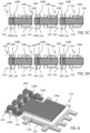
- Figure 6 shows a perspective view of an assembly of the leadframe 112, integrated circuit die 124 and clip 128 at the stage of the manufacturing process shown in Figure 3C .
- bonding pads of the integrated circuit die 124 may be electrically connected to upper surfaces at the distal ends of the lead regions 116 of the leadframe 12 by bonding wires (not explicitly shown) or through use of one or more other clips 128 as shown in Figure 6 .
- Figure 3D the assembly of the leadframe 112, integrated circuit dies 124 and clips 128 is then positioned within the open cavity 134 of a mold 136.
- Figure 3E - a resin encapsulant material is injected into the open cavity 134 and cured to form an encapsulating body 138 that encapsulates the assembly of the leadframe 112, integrated circuit dies 124 and clips 128, including filling the half-etched openings 120a, 120b and through openings 122 of the leadframe 112.
- Figure 3G - a saw (schematically represented by arrow 140) is used to partially cut into the encapsulated assembly from a lower surface thereof to form a channel 142.
- This saw cut is aligned with the half-etched opening 120b and passes completely through the leadframe 112 to separate the die pad region 115 and lead region 116 of each frame portion 114.
- the depth of the channel 142 made by the saw cut is sufficient to remove a portion of the cured resin encapsulant material that is located between the first and second vertical legs of the bridge portion 128c of the metal clip 128 without severing the horizontal leg which extends between the first and second vertical legs.
- half-etched opening 120b is optional, it will be understood that in cases where the half-etched opening 120b is not present to assist with saw 140 alignment that other means must be used to ensure that the saw cut is accurately positioned to form channel 142 at the location between the first and second vertical legs of the bridge portion 128c of the metal clip 128.
- Figure 3H - a plating process is then performed to plate a tin layer 144 on the exposed surfaces of the leadframe 112.
- exposed surfaces would include, for example, the lower surfaces of the die pad region 115, the lower surfaces of the lead region 116 of each frame portion 114 of the leadframe 12, and the sidewalls of the die pad region 115 and lead region 116 at the channel 142.
- the metal clips 128 provide electrical connections among and between all of the frame portions 114 of the etched leadframe 112. An advantage of this is that all frame portions 114 can be placed at the same electrical potential in connection with the performance of an electroplating process in the manufacturing step of Figure 3H to deposit the tin layer 144.
- FIG. 3I - a saw (schematically represented by arrow 146) is used to completely cut through the encapsulated assembly from an upper surface thereof and form separation opening 148. This saw cut is aligned with the location of the saw cut which formed the channel 142. This cutting operation effectuates a singulation of the encapsulated assembly into a plurality of power leadframe packages 150.
- the saw cut is made through the horizontal leg of the bridge portion 128c of the metal clip 128, and thus leaves opposed residual parts 158 of the bridge portion 128c with cut ends of the horizontal leg of the bridge portion 128c exposed at peripheral side surfaces of each power leadframe package 150.
- Figure 5D shows a top view (without the encapsulant present) of a portion of the leadframe 112 with attached integrated circuit dies 124 and mounted metal clips 128 at the stage of the manufacturing process shown in Figure 3I .
- a width of the saw cut performed by saw 146 is smaller than a width of the saw cut performed by saw 140.
- Figure 4 shows a cross-sectional view of the power leadframe package 150.
- the flank area 154 of the leads 152 and die pad 153 for the power leadframe package presents a fully wettable flank portion 156 (covered by the tin layer 144).
- the entire sidewall surfaces for the package leads 152 and die pad 153 were exposed by the saw cut in the step shown in Figure 3G and as a result the electroplating process covered the entire sidewall surfaces with the tin layer 144.
- This power leadframe package 150 accordingly includes a fully-wettable sidewall for the package leads 152 and die pad 153.
- each power leadframe package 150 provides a clear indication that the horizontal leg of the bridge portion 128c of the metal clip 128 was present during manufacturing and severed during the singulation process.
- the lateral offset of the peripheral sidewall of the package relative to the fully-wettable sidewall for the package leads 152 and die pad 153 provides a clear indication of the use of two separate cuts during manufacturing.
- the included residual parts 158 are positioned (and exposed) at opposite peripheral side surfaces of the encapsulating body.
- One of the residual parts 158 is part of a (first) metal clip that is mounted to the integrated circuit die of the illustrated package 150 and the other of the residual parts 158 is part of a (second) metal clip that is mounted to the integrated circuit die another (not illustrated) illustrated package 150 (see, Figure 3I ) severed from each other during the singulation process.
- the fully wettable sidewall for the package leads 152 and the fully wettable sidewall for die pad 153 are provided at the corresponding opposite peripheral side surfaces of the encapsulating body.
- the integrated circuit die 124 is a power metal oxide semiconductor field effect transistor (MOSFET) and the one or more metal clips 128 included in the package 150 support a high current capacity associated with the source/drain region of the MOSFET.
- MOSFET power metal oxide semiconductor field effect transistor
- the opening 148 severed die pad region 115 provides a current conduction lead (die pad) for the drain terminal of the MOSFET and the opening 148 severed lead region 116 along with metal clip 128 provides a current conduction lead for the source terminal of the MOSFET.
- lead structure of the leadframe 112 for the gate terminal would be present and that lead structure could, for example, be electrically connected to a gate bonding pad of the integrated circuit die 124 using convention wire bonding (like that shown in Figure 1C ).
- a smaller (for example, narrower) metal clip 128 could be used for the electrical connection of the gate bonding pad to the lead structure of the leadframe 112 (as shown in Figure 6 ).
- clip 128 can include multiple chip mounting portions 128a, lead mounting portions 128b and bridge portions 128c.
- the larger chip mounting portion 128a is configured for connection to a power transistor source/drain region of the integrated circuit die 124 while the smaller chip mounting portion 128a is configured for connection to a transistor gate region of the integrated circuit die 124.
- Advantages of the method of Figures 3A-3I and the power leadframe package 150 of Figure 4 include, at least, the following: a) the entire sidewall surface for the package leads 152 is solderable and/or solder wettable; b) a stronger solder joint can be made between the power leadframe package 150 and a supporting substrate (such as a printed circuit board); c) the presence of side solder required for automated solder inspection is ensured; d) a simple electroplating process is supported for depositing the tin layer, and this is less expensive that the use of electroless plating; and e) there is an improved performance in terms of lead anchoring.
Landscapes
- Lead Frames For Integrated Circuits (AREA)
Abstract
Description
- This application claims priority from
United States Provisional Application for Patent No. 63/444,721, filed February 10, 2023 - The present invention generally relates to semiconductor packaging and, more particularly, to a power leadframe package with leads having sidewall surfaces that are fully solder wettable.
- Reference is made to
Figures 1A -1L which show steps of a manufacturing process for producing a power leadframe package for an integrated circuit power transistor device. -
Figure 1A - provision is made from a manufacturer or supplier of anetched leadframe 12 that includes diepad portions 14 andlead portions 16. Thedie pad portions 14 andlead portions 16 are separated from each other by spaces defined by a half-etched opening 20 at the bottom of the leadframe and a through opening 22 at the top of the leadframe. -
Figure 1B - anintegrated circuit die 24 is mounted to the upper surface of eachdie pad portion 14. This attachment may, for example, be made using a suitabledie attachment mechanism 26. As an example, a die attach film, a layer of adhesive, or a layer of solder could be used for attachment. -
Figure 1C - bonding pads at an upper surface of the integratedcircuit die 24 are electrically connected to upper surfaces at thedistal ends 30 of thelead portions 16 of theleadframe 12 bybonding wires 28. -
Figure 1D - the assembly of theleadframe 12, integrated circuit dies 24 andbonding wires 28 is then positioned within theopen cavity 34 of amold 36. -
Figure 1E - a resin encapsulant material is injected into theopen cavity 34 and cured to form anencapsulating body 38 that encapsulates the assembly of theleadframe 12, integrated circuit dies 24 andbonding wires 28, including filling the half-etchedopenings 20 and throughopenings 22 of theleadframe 12. -
Figure 1F - the encapsulated assembly is removed from themold 36. -
Figure 1G - a saw (schematically represented by arrow 40) is used to partially cut through thelead portions 16 of theleadframe 12 to form achannel 42. The depth of thechannel 42 may, for example, comprise between 40 and 60 percent of the overall thickness of thelead portions 16 of theleadframe 12. -
Figure 1H - an electroless plating process is then performed to plate atin layer 44 on the exposed surfaces of theleadframe 12. These exposed surfaces would include, for example, the lower surfaces of thedie pad portions 14 of theleadframe 12, the lower surfaces of thelead portions 16 of theleadframe 12, and the sidewalls and bottom of thechannel 42 formed in thelead portions 16 of theleadframe 12. -
Figure 1I - a saw (schematically represented by arrow 46) is used to completely cut through the encapsulated assembly and form aseparation opening 48. This saw cut is aligned with the location of the saw cut which formed thechannel 42. This cutting operation effectuates a singulation of the encapsulated assembly into a plurality ofpower leadframe packages 50. A width of the saw cut performed bysaw 46 is smaller than a width of the saw cut performed by saw 40. -
Figure 2 shows a cross-sectional view of thepower leadframe package 50. It will be noted that theflank area 54 of the leads 52 (i.e., their sidewall surfaces) for thepower leadframe package 50 includes a wettable flank portion 56 (covered by the tin layer 44) and a non-wettable flank portion 58 (exposed by the saw cut in the step shown inFigure 1I ). As a result, thispower leadframe package 50 does not present a fully-wettable sidewall for the package leads 52. - There is a need in the art to address this deficiency and provide a power leadframe package with leads having sidewall surfaces that are fully solder wettable.
- In an embodiment, a method comprises: providing an etched leadframe that includes a plurality of frame portions, wherein the frame portions are separated from each other by spaces, and wherein each frame portion includes an intermediate region interposed between a lead region and a die pad region; mounting an integrated circuit die to an upper surface of each frame portion at said die pad region; mounting a chip mounting portion of a metal clip to each integrated circuit die, said metal clip further including a lead mounting portion mounted to the lead region of an adjacent frame portion, and said metal clip still further including a bridge portion extending over said intermediate region of said adjacent frame portion and mounted to the die pad region of said adjacent frame portion; performing a first operation to cut through the frame portion of each etched leadframe at said intermediate region to separate the lead region and die pad region without severing the bridge portion of each metal clip; plating a conductive layer on full sidewalls of the lead region and die pad region exposed by the first operation to cut; and performing a second operation to cut through the bridge portion of each metal clip.
- In an embodiment, a power leadframe integrated circuit package comprises: a leadframe including a lead region and a die pad region separated by a space; an integrated circuit die mounted to an upper surface of the die pad region; a first metal clip having a chip mounting portion mounted to the integrated circuit die, said first metal clip further including a lead mounting portion mounted to the lead region and a first residual bridge portion; a second metal clip including a second residual bridge portion mounted to the die pad region; an encapsulating body encapsulating the leadframe, the integrated circuit die and the first and second metal clips; wherein said encapsulating body has a first peripheral sidewall at which an end of said first residual bridge portion is exposed and has a second peripheral sidewall, opposite said first peripheral sidewall, at which an end of said second residual bridge portion is exposed; wherein a sidewall of the lead region is exposed at said first peripheral sidewall of the encapsulating body, and wherein a sidewall of the die pad region is exposed at said second peripheral sidewall of the encapsulating body; and a plating layer on all of said sidewall of the lead region and all of said sidewall of the die pad region.
- For a better understanding of the embodiments, reference will now be made by way of example only to the accompanying figures in which:
-
Figures 1A-1I show steps of a manufacturing process for producing a power leadframe package for an integrated circuit power transistor device; -
Figure 2 shows a power leadframe package produced by the process ofFigures 1A-1I ; -
Figures 3A-3I show steps of a manufacturing process for producing a power leadframe package for an integrated circuit power transistor device; -
Figure 4 shows a power leadframe package produced by the process ofFigures 3A-3I ; -
Figures 5A-5D show top views at the stage of the manufacturing process shown at steps corresponding toFigures 3A, 3B ,3C and3I , respectively; and -
Figure 6 is a perspective view of an assembly of a leadframe, integrated circuit die and clip at the stage of the manufacturing process shown at the step corresponding toFigure 3C . - Reference is made to
Figures 3A-3I which show steps of a manufacturing process for producing a power leadframe package for an integrated circuit power transistor device. -
Figure 3A - provision is made from a manufacturer or supplier of anetched leadframe 112 that includesframe portions 114. Theframe portions 114 are separated from each other by spaces defined by a half-etched opening 120a at the bottom of the leadframe and a through opening 122 at the top of the leadframe. A further half-etched opening 120b at the bottom of the leadframe is optionally provided at an intermediate region (of each frame portion 114) located between adie pad region 115 andlead region 116 of eachframe portion 114. It will be noted, however, that the optionally provided further half-etched opening 120b does not separate thedie pad region 115 andlead region 116.Figure 5A shows a top view of a portion of theleadframe 112 at the stage of the manufacturing process shown inFigure 3A . -
Figure 3B - anintegrated circuit die 124 is mounted to the upper surface of eachframe portion 114 at thedie pad region 115. This attachment may, for example, be made using a suitabledie attachment mechanism 126. As an example, a die attach film, a layer of adhesive, or a layer of solder could be used for attachment.Figure 5B shows a top view of a portion of theleadframe 112 with attachedintegrated circuit dies 124 at the stage of the manufacturing process shown inFigure 3B . -
Figure 3C - bonding pads at an upper surface of theintegrated circuit die 124 mounted to thedie pad region 115 of one frame portion (for example, portion 114a) of thelead frame 112 are electrically connected to upper surfaces at thelead regions 116 of an adjacent frame portion (for example, portion 114b) of theleadframe 112 and further to thedie pad region 115 of that adjacent frame portion 114b of theleadframe 112 using ametal clip 128. Themetal clip 128 comprises a strip of material that is bent into a shape that includes achip mounting portion 128a, alead mounting portion 128b and abridge portion 128c. Thechip mounting portion 128a is essentially a flat portion having a lower surface that is electrically connected by asolder material 129 to bonding pads of the integrated circuit die 124. Thelead mounting portion 128b is essentially an L-shaped portion having a vertical leg and a horizontal leg; where the vertical leg extends downwardly from thechip mounting portion 128a towards theleadframe 112 and the horizontal leg has a lower surface that is electrically connected by asolder material 129 to the upper surface at thelead region 116 of the adjacent frame portion 114b of theleadframe 112. Thebridge portion 128c is essentially an upside-down U-shaped portion having a first vertical leg, a horizontal leg and a second vertical leg; where the first vertical leg extends upwardly from the horizontal leg of thelead mounting portion 128b, the horizontal leg extends from the first vertical leg to bridge over the location of the further half-etchedopening 120b, and the second vertical leg extends downwardly from the horizontal leg and has an end surface electrically connected by asolder material 129 to the upper surface at thedie pad region 115 of the adjacent frame portion 114b of theleadframe 112.Figure 5C shows a top view of a portion of theleadframe 112 with attachedintegrated circuit dies 124 and mountedmetal clips 128 at the stage of the manufacturing process shown inFigure 3C .Figure 6 shows a perspective view of an assembly of theleadframe 112,integrated circuit die 124 andclip 128 at the stage of the manufacturing process shown inFigure 3C . - It will be noted that other bonding pads of the integrated
circuit die 124 may be electrically connected to upper surfaces at the distal ends of thelead regions 116 of theleadframe 12 by bonding wires (not explicitly shown) or through use of one or moreother clips 128 as shown inFigure 6 . -
Figure 3D - the assembly of theleadframe 112, integrated circuit dies 124 andclips 128 is then positioned within theopen cavity 134 of amold 136. -
Figure 3E - a resin encapsulant material is injected into theopen cavity 134 and cured to form anencapsulating body 138 that encapsulates the assembly of theleadframe 112, integrated circuit dies 124 andclips 128, including filling the half-etchedopenings openings 122 of theleadframe 112. -
Figure 3F - the encapsulated assembly is removed from themold 136. -
Figure 3G - a saw (schematically represented by arrow 140) is used to partially cut into the encapsulated assembly from a lower surface thereof to form achannel 142. This saw cut is aligned with the half-etched opening 120b and passes completely through theleadframe 112 to separate thedie pad region 115 andlead region 116 of eachframe portion 114. The depth of thechannel 142 made by the saw cut is sufficient to remove a portion of the cured resin encapsulant material that is located between the first and second vertical legs of thebridge portion 128c of themetal clip 128 without severing the horizontal leg which extends between the first and second vertical legs. As the presence of the half-etched opening 120b is optional, it will be understood that in cases where the half-etched opening 120b is not present to assist with saw 140 alignment that other means must be used to ensure that the saw cut is accurately positioned to formchannel 142 at the location between the first and second vertical legs of thebridge portion 128c of themetal clip 128. -
Figure 3H - a plating process is then performed to plate atin layer 144 on the exposed surfaces of theleadframe 112. These exposed surfaces would include, for example, the lower surfaces of thedie pad region 115, the lower surfaces of thelead region 116 of eachframe portion 114 of theleadframe 12, and the sidewalls of thedie pad region 115 andlead region 116 at thechannel 142. - It will be noted that the metal clips 128 provide electrical connections among and between all of the
frame portions 114 of the etchedleadframe 112. An advantage of this is that allframe portions 114 can be placed at the same electrical potential in connection with the performance of an electroplating process in the manufacturing step ofFigure 3H to deposit thetin layer 144. -
Figure 3I - a saw (schematically represented by arrow 146) is used to completely cut through the encapsulated assembly from an upper surface thereof andform separation opening 148. This saw cut is aligned with the location of the saw cut which formed thechannel 142. This cutting operation effectuates a singulation of the encapsulated assembly into a plurality of power leadframe packages 150. The saw cut is made through the horizontal leg of thebridge portion 128c of themetal clip 128, and thus leaves opposedresidual parts 158 of thebridge portion 128c with cut ends of the horizontal leg of thebridge portion 128c exposed at peripheral side surfaces of eachpower leadframe package 150.Figure 5D shows a top view (without the encapsulant present) of a portion of theleadframe 112 with attached integrated circuit dies 124 and mountedmetal clips 128 at the stage of the manufacturing process shown inFigure 3I . A width of the saw cut performed bysaw 146 is smaller than a width of the saw cut performed bysaw 140. -
Figure 4 shows a cross-sectional view of thepower leadframe package 150. It will be noted that the flank area 154 of theleads 152 and diepad 153 for the power leadframe package presents a fully wettable flank portion 156 (covered by the tin layer 144). The entire sidewall surfaces for the package leads 152 and diepad 153 were exposed by the saw cut in the step shown inFigure 3G and as a result the electroplating process covered the entire sidewall surfaces with thetin layer 144. Thispower leadframe package 150 accordingly includes a fully-wettable sidewall for the package leads 152 and diepad 153. The cut ends of the horizontal leg of thebridge portion 128c which are exposed at peripheral side surfaces of eachpower leadframe package 150 provide a clear indication that the horizontal leg of thebridge portion 128c of themetal clip 128 was present during manufacturing and severed during the singulation process. The lateral offset of the peripheral sidewall of the package relative to the fully-wettable sidewall for the package leads 152 and diepad 153 provides a clear indication of the use of two separate cuts during manufacturing. - In the context of
Figure 4 , the includedresidual parts 158 are positioned (and exposed) at opposite peripheral side surfaces of the encapsulating body. One of theresidual parts 158 is part of a (first) metal clip that is mounted to the integrated circuit die of the illustratedpackage 150 and the other of theresidual parts 158 is part of a (second) metal clip that is mounted to the integrated circuit die another (not illustrated) illustrated package 150 (see,Figure 3I ) severed from each other during the singulation process. The fully wettable sidewall for the package leads 152 and the fully wettable sidewall fordie pad 153 are provided at the corresponding opposite peripheral side surfaces of the encapsulating body. - In a preferred embodiment, the integrated circuit die 124 is a power metal oxide semiconductor field effect transistor (MOSFET) and the one or
more metal clips 128 included in thepackage 150 support a high current capacity associated with the source/drain region of the MOSFET. In particular, theopening 148 severeddie pad region 115 provides a current conduction lead (die pad) for the drain terminal of the MOSFET and theopening 148 severedlead region 116 along withmetal clip 128 provides a current conduction lead for the source terminal of the MOSFET. It will, of course, be understood that a lead structure of theleadframe 112 for the gate terminal (seeFigure 6 ) would be present and that lead structure could, for example, be electrically connected to a gate bonding pad of the integrated circuit die 124 using convention wire bonding (like that shown inFigure 1C ). Alternatively, a smaller (for example, narrower)metal clip 128 could be used for the electrical connection of the gate bonding pad to the lead structure of the leadframe 112 (as shown inFigure 6 ). - With reference to the perspective view shown in
Figure 6 , it will also be noted thatclip 128 can include multiplechip mounting portions 128a, lead mountingportions 128b andbridge portions 128c. In this case, for example, the largerchip mounting portion 128a is configured for connection to a power transistor source/drain region of the integrated circuit die 124 while the smallerchip mounting portion 128a is configured for connection to a transistor gate region of the integrated circuit die 124. - Advantages of the method of
Figures 3A-3I and thepower leadframe package 150 ofFigure 4 include, at least, the following: a) the entire sidewall surface for the package leads 152 is solderable and/or solder wettable; b) a stronger solder joint can be made between thepower leadframe package 150 and a supporting substrate (such as a printed circuit board); c) the presence of side solder required for automated solder inspection is ensured; d) a simple electroplating process is supported for depositing the tin layer, and this is less expensive that the use of electroless plating; and e) there is an improved performance in terms of lead anchoring. - While the invention has been illustrated and described in detail in the drawings and foregoing description, such illustration and description are considered illustrative or exemplary and not restrictive; the invention is not limited to the disclosed embodiments. Other variations to the disclosed embodiments can be understood and effected by those skilled in the art in practicing the claimed invention, from a study of the drawings, the disclosure, and the appended claims.
Claims (19)
- A method, comprising:providing an etched leadframe that includes a plurality of frame portions, wherein the frame portions are separated from each other by spaces, and wherein each frame portion includes an intermediate region interposed between a lead region and a die pad region;mounting an integrated circuit die to an upper surface of each frame portion at said die pad region;mounting a chip mounting portion of a metal clip to each integrated circuit die, said metal clip further including a lead mounting portion mounted to the lead region of an adjacent frame portion, and said metal clip still further including a bridge portion extending over said intermediate region of said adjacent frame portion and mounted to the die pad region of said adjacent frame portion;performing a first operation to cut through the frame portion of each etched leadframe at said intermediate region to separate the lead region and die pad region without severing the bridge portion of each metal clip;plating a conductive layer on full sidewalls of the lead region and die pad region exposed by the first operation to cut; andperforming a second operation to cut through the bridge portion of each metal clip.
- The method of claim 1, wherein performing the first operation to cut comprises sawing.
- The method of claim 1, wherein performing the second operation to cut comprises sawing.
- The method of claim 1, wherein plating the conductive layer comprises performing an electroplating.
- The method of claim 4, wherein electroplating comprises applying a potential to the lead regions and die pad regions of all frame portions of the leadframe through an electrical connection provided by the metal clips.
- The method of claim 1, wherein plating the conductive layer further comprises plating the conductive layer on bottom surfaces of the lead regions and die pad regions of all frame portions of the leadframe.
- The method of claim 1, further comprising encapsulating an assembly formed by the etched leadframe, mounted integrated circuits and mounted metal clips in an encapsulating material forming an encapsulating body.
- The method of claim 7, wherein performing the first operation to cut further cuts through a portion of the encapsulating material forming the encapsulating body that is located between the bridge portion of each metal clip and the intermediate region of the frame portions of the leadframe.
- The method of claim 8, wherein performing the first operation to cut comprises applying the cut to a lower surface of the encapsulating body at the intermediate region.
- The method of claim 7, wherein performing the second operation to cut further cuts through a portion of the encapsulating material forming the encapsulating body that is located between the bridge portion of each metal clip and an upper surface of the encapsulating body.
- The method of claim 10, wherein performing the second operation to cut comprises applying the cut to the upper surface of the encapsulating body.
- The method of claim 1, wherein providing the etched leadframe further comprises providing a channel at a lower surface of each frame portion at the intermediate region.
- The method of claim 12, wherein performing the first operation to cut comprises aligning the first operation to cut with the channel at the lower surface of each frame portion.
- A power leadframe integrated circuit package, comprising:a leadframe including a lead region and a die pad region separated by a space;an integrated circuit die mounted to an upper surface of the die pad region;a first metal clip having a chip mounting portion mounted to the integrated circuit die, said first metal clip further including a lead mounting portion mounted to the lead region and a first residual bridge portion;a second metal clip including a second residual bridge portion mounted to the die pad region;an encapsulating body encapsulating the leadframe, the integrated circuit die and the first and second metal clips;wherein said encapsulating body has a first peripheral sidewall at which an end of said first residual bridge portion is exposed and has a second peripheral sidewall, opposite said first peripheral sidewall, at which an end of said second residual bridge portion is exposed;wherein a sidewall of the lead region is exposed at said first peripheral sidewall of the encapsulating body, and wherein a sidewall of the die pad region is exposed at said second peripheral sidewall of the encapsulating body; anda plating layer on all of said sidewall of the lead region and all of said sidewall of the die pad region.
- The power leadframe integrated circuit package of claim 14, wherein said integrated circuit die comprises a power metal oxide semiconductor field effect transistor (MOSFET) and wherein said first metal clip provides a high current capacity associated with a source region or drain region of the MOSFET.
- The power leadframe integrated circuit package of claim 14, wherein the plating layer is a tin layer.
- The power leadframe integrated circuit package of claim 14, wherein the plating layer further extends on lower surfaces of the lead region and die pad region.
- The power leadframe integrated circuit package of claim 14, wherein the second residual bridge portion is a singulation severed part of the first metal clip for another power leadframe integrated circuit package.
- The power leadframe integrated circuit package of claim 14, wherein the first residual bridge portion is a singulation severed part of the second metal clip for another power leadframe integrated circuit package.
Applications Claiming Priority (2)
| Application Number | Priority Date | Filing Date | Title |
|---|---|---|---|
| US202363444721P | 2023-02-10 | 2023-02-10 | |
| US18/415,006 US20240274572A1 (en) | 2023-02-10 | 2024-01-17 | Power leadframe package with lead sidewall surface that is fully solder wettable |
Publications (3)
| Publication Number | Publication Date |
|---|---|
| EP4415042A2 true EP4415042A2 (en) | 2024-08-14 |
| EP4415042A3 EP4415042A3 (en) | 2024-10-30 |
| EP4415042B1 EP4415042B1 (en) | 2025-10-15 |
Family
ID=89767355
Family Applications (1)
| Application Number | Title | Priority Date | Filing Date |
|---|---|---|---|
| EP24154067.3A Active EP4415042B1 (en) | 2023-02-10 | 2024-01-26 | Power leadframe package with lead sidewall surface that is fully solder wettable |
Country Status (3)
| Country | Link |
|---|---|
| US (1) | US20240274572A1 (en) |
| EP (1) | EP4415042B1 (en) |
| CN (1) | CN222146213U (en) |
Family Cites Families (4)
| Publication number | Priority date | Publication date | Assignee | Title |
|---|---|---|---|---|
| US8076181B1 (en) * | 2010-10-22 | 2011-12-13 | Linear Technology Corporation | Lead plating technique for singulated IC packages |
| CN102789994B (en) * | 2011-05-18 | 2016-08-10 | 飞思卡尔半导体公司 | The wettable semiconductor device in side |
| US10121742B2 (en) * | 2017-03-15 | 2018-11-06 | Amkor Technology, Inc. | Method of forming a packaged semiconductor device using ganged conductive connective assembly and structure |
| CN113035722A (en) * | 2019-12-24 | 2021-06-25 | 维谢综合半导体有限责任公司 | Packaging process for plating with selective molding |
-
2024
- 2024-01-17 US US18/415,006 patent/US20240274572A1/en active Pending
- 2024-01-26 EP EP24154067.3A patent/EP4415042B1/en active Active
- 2024-02-07 CN CN202420288053.7U patent/CN222146213U/en active Active
Also Published As
| Publication number | Publication date |
|---|---|
| EP4415042B1 (en) | 2025-10-15 |
| CN222146213U (en) | 2024-12-10 |
| EP4415042A3 (en) | 2024-10-30 |
| US20240274572A1 (en) | 2024-08-15 |
Similar Documents
| Publication | Publication Date | Title |
|---|---|---|
| US7410834B2 (en) | Method of manufacturing a semiconductor device | |
| US8344499B2 (en) | Chip-exposed semiconductor device | |
| US7838340B2 (en) | Pre-molded clip structure | |
| US9287202B2 (en) | Resin-encapsulated semiconductor device and its manufacturing method | |
| KR20080070068A (en) | Semiconductor die package and its manufacturing method using lead frame and clip | |
| CN101556946B (en) | Method of forming a semiconductor package and structure thereof | |
| US12575429B2 (en) | Semiconductor package having a lead frame and a clip frame | |
| WO2007067998A2 (en) | Device and method for assembling a top and bottom exposed packaged semiconductor | |
| KR20160006608A (en) | Lead frame, semiconductor device, and method for manufacturing lead frame | |
| US12119263B2 (en) | Methods and apparatus for an improved integrated circuit package | |
| CN113496975A (en) | Semiconductor package and manufacturing method thereof | |
| US12444667B2 (en) | Semiconductor device and method for manufacturing semiconductor device | |
| EP2973690B1 (en) | Stack die package | |
| CN103325699B (en) | Manufacturing method of semiconductor device | |
| US11145578B2 (en) | Semiconductor package with top or bottom side cooling and method for manufacturing the semiconductor package | |
| EP4415042B1 (en) | Power leadframe package with lead sidewall surface that is fully solder wettable | |
| CN114520203A (en) | Contact clip for semiconductor device package | |
| JP7824231B2 (en) | Semiconductor device manufacturing method and semiconductor device | |
| CN118507362A (en) | Power lead frame package with fully solder wettable lead sidewall surfaces | |
| CN117316911A (en) | Semiconductor package with wettable lead sides and connecting rods and method of manufacturing same | |
| US20250201673A1 (en) | Semiconductor device and method of manufacturing the same | |
| US20240170373A1 (en) | Semiconductor device | |
| CN121666102A (en) | Semiconductor packages with wettable side wings and related methods | |
| JP4822660B2 (en) | Micro joint terminal for semiconductor connection | |
| CN110892527B (en) | Semiconductor device and method of manufacturing semiconductor device |
Legal Events
| Date | Code | Title | Description |
|---|---|---|---|
| PUAI | Public reference made under article 153(3) epc to a published international application that has entered the european phase |
Free format text: ORIGINAL CODE: 0009012 |
|
| STAA | Information on the status of an ep patent application or granted ep patent |
Free format text: STATUS: REQUEST FOR EXAMINATION WAS MADE |
|
| 17P | Request for examination filed |
Effective date: 20240126 |
|
| AK | Designated contracting states |
Kind code of ref document: A2 Designated state(s): AL AT BE BG CH CY CZ DE DK EE ES FI FR GB GR HR HU IE IS IT LI LT LU LV MC ME MK MT NL NO PL PT RO RS SE SI SK SM TR |
|
| PUAL | Search report despatched |
Free format text: ORIGINAL CODE: 0009013 |
|
| AK | Designated contracting states |
Kind code of ref document: A3 Designated state(s): AL AT BE BG CH CY CZ DE DK EE ES FI FR GB GR HR HU IE IS IT LI LT LU LV MC ME MK MT NL NO PL PT RO RS SE SI SK SM TR |
|
| RIC1 | Information provided on ipc code assigned before grant |
Ipc: H01L 21/56 20060101ALI20240924BHEP Ipc: H01L 23/495 20060101AFI20240924BHEP |
|
| GRAP | Despatch of communication of intention to grant a patent |
Free format text: ORIGINAL CODE: EPIDOSNIGR1 |
|
| STAA | Information on the status of an ep patent application or granted ep patent |
Free format text: STATUS: GRANT OF PATENT IS INTENDED |
|
| INTG | Intention to grant announced |
Effective date: 20250514 |
|
| RIN1 | Information on inventor provided before grant (corrected) |
Inventor name: TALLEDO, JEFFERSON SISMUNDO |
|
| GRAS | Grant fee paid |
Free format text: ORIGINAL CODE: EPIDOSNIGR3 |
|
| GRAA | (expected) grant |
Free format text: ORIGINAL CODE: 0009210 |
|
| STAA | Information on the status of an ep patent application or granted ep patent |
Free format text: STATUS: THE PATENT HAS BEEN GRANTED |
|
| AK | Designated contracting states |
Kind code of ref document: B1 Designated state(s): AL AT BE BG CH CY CZ DE DK EE ES FI FR GB GR HR HU IE IS IT LI LT LU LV MC ME MK MT NL NO PL PT RO RS SE SI SK SM TR |
|
| REG | Reference to a national code |
Ref country code: GB Ref legal event code: FG4D Ref country code: CH Ref legal event code: F10 Free format text: ST27 STATUS EVENT CODE: U-0-0-F10-F00 (AS PROVIDED BY THE NATIONAL OFFICE) Effective date: 20251015 |
|
| REG | Reference to a national code |
Ref country code: DE Ref legal event code: R096 Ref document number: 602024000878 Country of ref document: DE |
|
| REG | Reference to a national code |
Ref country code: IE Ref legal event code: FG4D |
|
| REG | Reference to a national code |
Ref country code: DE Ref legal event code: R079 Ref document number: 602024000878 Country of ref document: DE Free format text: PREVIOUS MAIN CLASS: H01L0023495000 Ipc: H10W0070400000 |
|
| REG | Reference to a national code |
Ref country code: NL Ref legal event code: MP Effective date: 20251015 |
|
| REG | Reference to a national code |
Ref country code: AT Ref legal event code: MK05 Ref document number: 1847819 Country of ref document: AT Kind code of ref document: T Effective date: 20251015 |
|
| PG25 | Lapsed in a contracting state [announced via postgrant information from national office to epo] |
Ref country code: NL Free format text: LAPSE BECAUSE OF FAILURE TO SUBMIT A TRANSLATION OF THE DESCRIPTION OR TO PAY THE FEE WITHIN THE PRESCRIBED TIME-LIMIT Effective date: 20251015 |
|
| PG25 | Lapsed in a contracting state [announced via postgrant information from national office to epo] |
Ref country code: ES Free format text: LAPSE BECAUSE OF FAILURE TO SUBMIT A TRANSLATION OF THE DESCRIPTION OR TO PAY THE FEE WITHIN THE PRESCRIBED TIME-LIMIT Effective date: 20251015 |
|
| REG | Reference to a national code |
Ref country code: LT Ref legal event code: MG9D |
|
| PG25 | Lapsed in a contracting state [announced via postgrant information from national office to epo] |
Ref country code: NO Free format text: LAPSE BECAUSE OF FAILURE TO SUBMIT A TRANSLATION OF THE DESCRIPTION OR TO PAY THE FEE WITHIN THE PRESCRIBED TIME-LIMIT Effective date: 20260115 |
|
| PGFP | Annual fee paid to national office [announced via postgrant information from national office to epo] |
Ref country code: DE Payment date: 20251217 Year of fee payment: 3 |
|
| PG25 | Lapsed in a contracting state [announced via postgrant information from national office to epo] |
Ref country code: FI Free format text: LAPSE BECAUSE OF FAILURE TO SUBMIT A TRANSLATION OF THE DESCRIPTION OR TO PAY THE FEE WITHIN THE PRESCRIBED TIME-LIMIT Effective date: 20251015 Ref country code: AT Free format text: LAPSE BECAUSE OF FAILURE TO SUBMIT A TRANSLATION OF THE DESCRIPTION OR TO PAY THE FEE WITHIN THE PRESCRIBED TIME-LIMIT Effective date: 20251015 Ref country code: HR Free format text: LAPSE BECAUSE OF FAILURE TO SUBMIT A TRANSLATION OF THE DESCRIPTION OR TO PAY THE FEE WITHIN THE PRESCRIBED TIME-LIMIT Effective date: 20251015 |
|
| PG25 | Lapsed in a contracting state [announced via postgrant information from national office to epo] |
Ref country code: RS Free format text: LAPSE BECAUSE OF FAILURE TO SUBMIT A TRANSLATION OF THE DESCRIPTION OR TO PAY THE FEE WITHIN THE PRESCRIBED TIME-LIMIT Effective date: 20260115 |
|
| PG25 | Lapsed in a contracting state [announced via postgrant information from national office to epo] |
Ref country code: IS Free format text: LAPSE BECAUSE OF FAILURE TO SUBMIT A TRANSLATION OF THE DESCRIPTION OR TO PAY THE FEE WITHIN THE PRESCRIBED TIME-LIMIT Effective date: 20260215 |
|
| PG25 | Lapsed in a contracting state [announced via postgrant information from national office to epo] |
Ref country code: PT Free format text: LAPSE BECAUSE OF FAILURE TO SUBMIT A TRANSLATION OF THE DESCRIPTION OR TO PAY THE FEE WITHIN THE PRESCRIBED TIME-LIMIT Effective date: 20260216 |
|
| PG25 | Lapsed in a contracting state [announced via postgrant information from national office to epo] |
Ref country code: PL Free format text: LAPSE BECAUSE OF FAILURE TO SUBMIT A TRANSLATION OF THE DESCRIPTION OR TO PAY THE FEE WITHIN THE PRESCRIBED TIME-LIMIT Effective date: 20251015 |
|
| PG25 | Lapsed in a contracting state [announced via postgrant information from national office to epo] |
Ref country code: LV Free format text: LAPSE BECAUSE OF FAILURE TO SUBMIT A TRANSLATION OF THE DESCRIPTION OR TO PAY THE FEE WITHIN THE PRESCRIBED TIME-LIMIT Effective date: 20251015 |
|
| PG25 | Lapsed in a contracting state [announced via postgrant information from national office to epo] |
Ref country code: BG Free format text: LAPSE BECAUSE OF FAILURE TO SUBMIT A TRANSLATION OF THE DESCRIPTION OR TO PAY THE FEE WITHIN THE PRESCRIBED TIME-LIMIT Effective date: 20251015 |