EP4414743A1 - Polarization switchable multi-zone illumination system using a polarization switchable light source and polarization sensitive optic - Google Patents
Polarization switchable multi-zone illumination system using a polarization switchable light source and polarization sensitive optic Download PDFInfo
- Publication number
- EP4414743A1 EP4414743A1 EP24155655.4A EP24155655A EP4414743A1 EP 4414743 A1 EP4414743 A1 EP 4414743A1 EP 24155655 A EP24155655 A EP 24155655A EP 4414743 A1 EP4414743 A1 EP 4414743A1
- Authority
- EP
- European Patent Office
- Prior art keywords
- light signal
- far field
- polarization
- polarization state
- zone
- Prior art date
- Legal status (The legal status is an assumption and is not a legal conclusion. Google has not performed a legal analysis and makes no representation as to the accuracy of the status listed.)
- Pending
Links
Images



Classifications
-
- G—PHYSICS
- G03—PHOTOGRAPHY; CINEMATOGRAPHY; ANALOGOUS TECHNIQUES USING WAVES OTHER THAN OPTICAL WAVES; ELECTROGRAPHY; HOLOGRAPHY
- G03B—APPARATUS OR ARRANGEMENTS FOR TAKING PHOTOGRAPHS OR FOR PROJECTING OR VIEWING THEM; APPARATUS OR ARRANGEMENTS EMPLOYING ANALOGOUS TECHNIQUES USING WAVES OTHER THAN OPTICAL WAVES; ACCESSORIES THEREFOR
- G03B21/00—Projectors or projection-type viewers; Accessories therefor
- G03B21/14—Details
- G03B21/20—Lamp housings
- G03B21/2073—Polarisers in the lamp house
-
- G—PHYSICS
- G01—MEASURING; TESTING
- G01B—MEASURING LENGTH, THICKNESS OR SIMILAR LINEAR DIMENSIONS; MEASURING ANGLES; MEASURING AREAS; MEASURING IRREGULARITIES OF SURFACES OR CONTOURS
- G01B11/00—Measuring arrangements characterised by the use of optical techniques
- G01B11/14—Measuring arrangements characterised by the use of optical techniques for measuring distance or clearance between spaced objects or spaced apertures
-
- G—PHYSICS
- G01—MEASURING; TESTING
- G01B—MEASURING LENGTH, THICKNESS OR SIMILAR LINEAR DIMENSIONS; MEASURING ANGLES; MEASURING AREAS; MEASURING IRREGULARITIES OF SURFACES OR CONTOURS
- G01B11/00—Measuring arrangements characterised by the use of optical techniques
- G01B11/22—Measuring arrangements characterised by the use of optical techniques for measuring depth
-
- G—PHYSICS
- G01—MEASURING; TESTING
- G01S—RADIO DIRECTION-FINDING; RADIO NAVIGATION; DETERMINING DISTANCE OR VELOCITY BY USE OF RADIO WAVES; LOCATING OR PRESENCE-DETECTING BY USE OF THE REFLECTION OR RERADIATION OF RADIO WAVES; ANALOGOUS ARRANGEMENTS USING OTHER WAVES
- G01S7/00—Details of systems according to groups G01S13/00, G01S15/00, G01S17/00
- G01S7/48—Details of systems according to groups G01S13/00, G01S15/00, G01S17/00 of systems according to group G01S17/00
- G01S7/481—Constructional features, e.g. arrangements of optical elements
- G01S7/4814—Constructional features, e.g. arrangements of optical elements of transmitters alone
- G01S7/4815—Constructional features, e.g. arrangements of optical elements of transmitters alone using multiple transmitters
-
- G—PHYSICS
- G02—OPTICS
- G02B—OPTICAL ELEMENTS, SYSTEMS OR APPARATUS
- G02B27/00—Optical systems or apparatus not provided for by any of the groups G02B1/00 - G02B26/00, G02B30/00
- G02B27/28—Optical systems or apparatus not provided for by any of the groups G02B1/00 - G02B26/00, G02B30/00 for polarising
- G02B27/283—Optical systems or apparatus not provided for by any of the groups G02B1/00 - G02B26/00, G02B30/00 for polarising used for beam splitting or combining
-
- G—PHYSICS
- G02—OPTICS
- G02B—OPTICAL ELEMENTS, SYSTEMS OR APPARATUS
- G02B27/00—Optical systems or apparatus not provided for by any of the groups G02B1/00 - G02B26/00, G02B30/00
- G02B27/42—Diffraction optics, i.e. systems including a diffractive element being designed for providing a diffractive effect
- G02B27/4261—Diffraction optics, i.e. systems including a diffractive element being designed for providing a diffractive effect having a diffractive element with major polarization dependent properties
-
- G—PHYSICS
- G02—OPTICS
- G02B—OPTICAL ELEMENTS, SYSTEMS OR APPARATUS
- G02B5/00—Optical elements other than lenses
- G02B5/18—Diffraction gratings
- G02B5/1833—Diffraction gratings comprising birefringent materials
-
- G—PHYSICS
- G03—PHOTOGRAPHY; CINEMATOGRAPHY; ANALOGOUS TECHNIQUES USING WAVES OTHER THAN OPTICAL WAVES; ELECTROGRAPHY; HOLOGRAPHY
- G03B—APPARATUS OR ARRANGEMENTS FOR TAKING PHOTOGRAPHS OR FOR PROJECTING OR VIEWING THEM; APPARATUS OR ARRANGEMENTS EMPLOYING ANALOGOUS TECHNIQUES USING WAVES OTHER THAN OPTICAL WAVES; ACCESSORIES THEREFOR
- G03B21/00—Projectors or projection-type viewers; Accessories therefor
- G03B21/14—Details
- G03B21/20—Lamp housings
- G03B21/2006—Lamp housings characterised by the light source
- G03B21/2033—LED or laser light sources
-
- G—PHYSICS
- G03—PHOTOGRAPHY; CINEMATOGRAPHY; ANALOGOUS TECHNIQUES USING WAVES OTHER THAN OPTICAL WAVES; ELECTROGRAPHY; HOLOGRAPHY
- G03B—APPARATUS OR ARRANGEMENTS FOR TAKING PHOTOGRAPHS OR FOR PROJECTING OR VIEWING THEM; APPARATUS OR ARRANGEMENTS EMPLOYING ANALOGOUS TECHNIQUES USING WAVES OTHER THAN OPTICAL WAVES; ACCESSORIES THEREFOR
- G03B21/00—Projectors or projection-type viewers; Accessories therefor
- G03B21/14—Details
- G03B21/20—Lamp housings
- G03B21/208—Homogenising, shaping of the illumination light
Definitions
- the present invention generally relates to illumination systems for sensors, such as time-of-flight sensors.
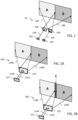
- FIG. 1 illustrates a block diagram of a multi-zone illumination system 10.
- the system 10 includes a first light source 12A associated with illumination of the far field zone A and a second light source 12B associated with illumination of the far field zone B.
- Light 14A emitted from the first light source 12A is directed through a first diffractive optical element (DOE) 16A and directed towards illumination 18A of the far field zone A.
- Light 14B emitted from the second light source 12B is directed through a second DOE 16B and directed towards illumination 18B of the far field zone B.
- DOE diffractive optical element
- a benefit of the system 10 solution is associated with laser safety concerns - if only a subsection of the overall scene is illuminated at any one time, a lower optical power is required for the light sources.
- a concern with the system 10 solution is the use of multiple components which introduce problems with increased cost, decreased yield due to system component alignment sensitivities, and larger packaging requirements.
- a device comprises: a multi-zone illumination system, wherein said multi-zone illumination system comprises: a light source including a first plurality of emitters configured to transmit a first light signal having a first polarization state, and a second plurality of emitters configured to transmit a second light signal having a second polarization state transverse to the first polarization state; and an optic configured to receive the first light signal and generate a first structured illumination of a first far field zone and receive the second light signal and generate a second structured illumination of a second far field zone; wherein the first and second far field zones are offset from each other.
- a method comprises: activating a first channel of a light source; transmitting, by the first channel of the light source, a first light signal having a first polarization state; generating, by an optic, a first structured illumination of a first far field zone in response to the first light signal; activating a second channel of the light source; transmitting, by the second channel of the light source, a second light signal having a second polarization state transverse to the first polarization state; and generating, by the optic, a second structured illumination of a second far field zone in response to the second light signal; wherein the first and second far field zones are offset from each other.
- the first/second structured illuminations may, for example, comprise the projection of a specific pattern (such as a dot or grid pattern) illumination in the far field zone or the projection of flood or substantially uniform or evenly spread illumination in the far field zone.
- a specific pattern such as a dot or grid pattern
- FIG. 2A illustrates a block diagram of a multi-zone illumination system 100.
- the system 100 includes a switchable polarization light source 112 that is controllable to emit light 114A having a first polarization (for example, TM polarized) associated with illumination of the far field zone A and emit light 114B having a second polarization, orthogonal to the first polarization (for example, TE polarized), associated with illumination of the far field zone B.
- TM polarized first polarization
- TE polarized orthogonal to the first polarization
- the light 114A, 114B emitted from the light source 112 is directed through a polarization sensitive diffractive optical element (DOE) 116.
- the DOE 116 directs the light 114A having the first polarization towards a structured illumination 118A of the far field zone A and directs the light 114B having the second polarization towards a structured illumination 118B of the far field zone B.
- DOE polarization sensitive diffractive optical element
- the DOE 116 may be configured so that there is a slight overlap (zone C) of the far field zone A and far field zone B.
- the provision of the slight overlap (zone C) is optional in some applications.
- the switchable polarization light source 112 employs a single two-channel emitter circuit with one channel for each of two orthogonal polarization states.
- the light source 112 may comprise, for example, a plurality of vertical-cavity surface-emitting laser (VCSEL) elements.
- VCSEL vertical-cavity surface-emitting laser
- the light source 112 is a dual channel light source that switches between a first channel where certain VCSEL elements emit the first light signal 114A having a first polarization state, and a second channel where other VCSEL elements emit the second light signal 114B having a second polarization state orthogonal to the first polarization state.
- the configuration of the switchable polarization light source 112 will be discussed in further detail below.
- the polarization sensitive DOE 116 comprises a metasurface-based polarization sensitive optic projecting each of the two illuminations as a function of the light source polarization state.
- the DOE 116 receives the light signal 114A (first polarization) transmitted by the light source 112 and produces a first structured illumination 118A pattern at the far field zone A, and receives the light signal 114B (second polarization) transmitted by the light source 112 and produces a second structured illumination 118B pattern at the far field zone B.
- the configuration of the DOE 116 will be discussed in further detail below.
- the switchable polarization light source 112 comprises a plurality of first laser (VCSEL) emitters that emit light of a first polarization to form a light signal 114A (see, Figures 2A and 2B ) and a plurality of second laser (VCSEL) emitters that emit light of a second polarization (orthogonal to the first polarization) to form a light signal 114B (see, Figures 2A and 2B ).
- the first and second laser (VCSEL) emitters may, for example, be arranged in an array format.
- the first and second laser (VCSEL) emitters may, for example, be interleaved with each other in a pattern.
- the light source 112 includes a plurality of laser (VCSEL) emitters 134A, 134B on a substrate 136.
- the substrate 136 may be a semiconductor substrate, printed circuit board, or another type of supporting structure.
- Each of the emitters 134A emits light of a first polarization to form a light signal 114A (see, Figures 2A and 2B ).
- Each of the emitters 134B emits light of a second polarization, orthogonal to the first polarization, to form a light signal 114B (see, Figures 2A and 2B ).
- the emitters 134A, 134B emit light in a direction along the z-axis. Stated differently, the light emitted by each of the emitters 134A, 134B propagates out of the page.
- the emitters 134A, 134B are arranged as an array in a number of alternating (interleaved) columns 138A, 138B positioned along the x-axis, with each of the columns 138A, 138B extending along the y-axis.
- Each of the columns 138A includes emitters 134A arranged in one or more sub-columns emitters.
- Each of the columns 138B includes emitters 134BA arranged in one or more sub-columns emitters. The emitters of each sub-column are aligned with each other along the y-axis.
- the columns 138A of emitters 134A are electrically coupled to each other through a circuit 144 to form a first emitter channel, and the columns 138B of emitters 134B are electrically coupled to each other through a circuit 146 to form a second emitter channel.
- the emitters 134A of the first emitter channel emit a light signal having a first linear polarization state.
- the emitters 134A of the first emitter channel emit a transverse magnetic (TM) polarized light signal with a magnetic field transverse to a propagation direction of the light signal.
- the emitters 134B of the second emitter channel emit a light signal having a second linear polarization state orthogonal to the first linear polarization state.
- the emitters 134B of the second emitter channel emit a transverse electric (TE) polarized light signal with an electric field transverse to the propagation direction of the light signal and transverse to the magnetic field of the light signal emitted by emitters of the first emitter channel.
- the light source 112 includes an array of emitters 134 per orthogonal polarization state.
- the emitters 134A of the first emitter channel and the emitters 134B of the second emitter channel may be configured to generate light in any wavelength range suited to the system application.
- the emitters 134A of the first emitter channel and the emitters 134B of the second emitter channel each have a wavelength between 900 and 1000 nanometers.
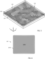
- Figure 4 is a top view of the polarization sensitive DOE 116 according to an embodiment disclosed herein.
- Figure 5 is a perspective view of the polarization sensitive DOE 116 according to an embodiment disclosed herein.
- the polarization sensitive DOE 116 is configured to receive the light signal 114A of the first polarization from the emitters 134A and produce a corresponding first structured illumination 118A pattern at the far field zone A.
- the polarization sensitive DOE 116 is configured to receive the light signal 114B of the second polarization from the emitters 134B and produce a corresponding second structured illumination 118B pattern at the far field zone B.
- the polarization sensitive DOE 116 can reduce the divergence requirement per function and support a scanning capability over multiple far fields within a scene. Additionally, per-channel assembly tolerance is greatly reduced as only a single optical alignment with the light source 112 is required.
- the first and second structured illumination pattern comprise dot or grid projector illuminations of the far field zone. In another example implementation, the first and second structured illumination pattern comprise flood illuminations of the far field zone.
- the polarization sensitive DOE 116 is a metasurface-based polarization sensitive optic with dual optical functions.
- transmission optical structures are implemented with diffractive optical elements (DOE) in subwavelength features that opportunely manipulate a light source output wave front into a specific far field intensity profile, such as flood or dot projection.
- DOE diffractive optical elements
- subwavelength dielectric nanostructures have become a remarkable candidate as a technological platform for a DOE, as optical metasurfaces are compatible with semiconductor fabrication processes (e.g., lithography), provide a potentially large number of phase quantization levels, and are suitable for the implementation of a variety of optical elements.
- a light polarization dependence can be also achieved, providing the possibility to encode different distinctive functionalities to the same optics dependent on light polarization, wherein those distinctive functionalities become accessible by the selection of a proper input polarization state for the received light signal.
- the polarization sensitive DOE 116 includes an array of asymmetrical nano meta-elements 121.
- the meta-elements 121 exhibit an asymmetry of features having various dimensions. For example, as shown in Figures 4 and 5 , a first set of the meta-elements 121 have a cross-sectional shape (in the x-y plane) with a major axis extending along the x-axis, a second set of the meta-elements 121 have a cross-sectional shape (in the x-y plane) with a major axis extending along the y-axis, and a third set of the meta-elements 121 have a cross-sectional shape (in the x-y plane) that is substantially circular with substantially equal dimensions along the x-axis and the y-axis. It will further noted that the first and second sets may each include sub-sets having different dimensions for the major and/or minor axes.
- the meta-elements 121 are fabricated by employing
- the meta-elements 121 are supported by a substrate 122 and are encapsulated by an encapsulation material 123 (such as silicon oxide).
- the polarization sensitive DOE 116 is positioned relative to the switchable polarization light source 112 such that the length of the meta-elements 121 axially extends in the propagation direction of the light signals 114A and 114B (i.e., along the direction of the x-axis).
- the meta-elements 121, supporting substrate and the included encapsulation material are made of one or more dielectric materials. In an embodiment, the meta-elements 121, supporting substrate and any included encapsulation material are made of different materials. In an embodiment, a delta between refractive indices of the materials used for the meta-elements 121, supporting substrate and any included encapsulation material is in a range between 1.5 and 2.
- the following parameters for the meta-elements 121 may be used, with reference to Figure 9 : scatterer shape - asymmetric truncated cone 300; scatterer material - polysilicon; on axis dimension range (302) - 120 to 360nm, both x-axis and y-axis, all combinations; lattice (304) - 470nm; height 306 - 700nm; SWA (308) - 92 degrees; and overetch (310) - -20nm.
- the supporting substrate for the meta-elements 121 may, for example, comprise one or more anti-reflective coating layers (312) and a silicon nitride layer( 314).
- the encapsulation material layer (316) may, for example, comprise silicon oxide.
- the polarization sensitive DOE 116 may exhibit the following optical specifications: effective focal length - 1145.8 ⁇ m; working distance - 991.4 ⁇ m; horizontal field of view - 42.3°; vertical field of view - 51.2°; transmission - >80%; and zeroth-order - ⁇ 0.3%.
- Structured illumination functionalities for two distinct (and possible partially overlapping) far field zones A and B are simultaneously implemented in the same physical DOE, namely the asymmetrical meta-elements 121 of the polarization sensitive DOE 116, by translating the functional design structured illuminations of the two far field zones into the physical design of the included nanostructures. For example, a translation from the required elements of the phase profile to appropriate shapes and dimensions of the asymmetrical meta-elements 121 is performed.
- the translation process may generally include simultaneously minimizing the delta between (1) the desired phase retardation to generate the two structured illuminations in specific optic coordinates and (2) the phase retardation provided in both the first and second polarizations (TM and TE polarization) of the light signals 114A and 114B by the meta-elements 121, represented by the meta-element dimensions along the x-axis and y axis.
- each of the meta-elements 121 displays a different optical behavior (e.g., transmission, phase retardation, etc.) as a function of incident polarization state (e.g., TM or TE polarization) of the received light signal and the dimensions of the meta-elements along the x-axis and y-axis.
- incident polarization state e.g., TM or TE polarization
- the dimensions of the meta-elements 121 along the x-axis and y axis are optimized to provide the proper phase retardation to generate a structured illumination pattern in the far field zone A from the light signal 114A generated by the first channel of the switchable polarization light source 112 in the first (TM) polarization, and provide the proper phase retardation to generate a structured illumination pattern in the far field zone B from the light signal 114B generated by the second channel of the switchable polarization light source 112 in the second (TE) polarization.
- the dimensions of the meta-elements 121 along the x-axis and y axis are selected to alter the phase of the light signal 114A transmitted by the first channel to transform the light in to a structured illumination projection pattern directed towards the far field zone A, and to alter the phase of the light signal 114B transmitted by the second channel to transform the light in to a structured illumination projection pattern directed towards the far field zone B.
- the emitters of the first channel emit a light signal 114A having a first linear polarization state (for example, TM polarized light); and the emitters of the second channel emit a light signal 114B having a second linear polarization state orthogonal to the first polarization state (for example, TE polarized light).
- the polarization sensitive DOE 116 projects a first and second structured illuminations 118A, 118B as a function of the polarization state of the light emitted by the switchable polarization light source 112.
- the polarization sensitive DOE 116 projects a structured illumination 118A projection pattern in the far field zone A upon receiving TM polarized light generated by the first channel, and projects a structured illumination 118B projection pattern in the far field zone B upon receiving TE polarized light generated by the second channel.
- structured illumination of two distinct, and partially overlapping, zones may be chosen by selection of the first channel or the second channel, respectively, of the switchable polarization light source 112.
- Figure 6 illustrates a structured illumination pattern 147 produced by the polarization sensitive DOE 116 according to an embodiment disclosed herein.
- the light in this structured illumination is relatively evenly (or uniformly) spread over a large central region 147a of space.
- a light gradient associated with edge regions 147b of the structured illumination pattern 147 may exist, in some implementations, a light gradient associated with edge regions 147b of the structured illumination pattern 147.
- the structured illumination pattern 147 in Figure 6 is representative of the illumination provided for each of the far field zone A and the far field zone B.
- the partial overlap of the zones A and B, as shown at with zone C in Figure 2B accounts for edge light gradient regions.
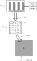
- Figure 7A and 7B illustrate the operation of the multi-zone illumination system 100.
- a dual channel driver selectively activates the first channel to turn on the plurality of laser emitters 134A of the light source 112.
- the emitters 134A of the first channel emit a light signal 114A having a first polarization state, such as TM polarized light, that is directed towards the polarization sensitive DOE 116.
- the meta-elements 121 of the polarization sensitive DOE 116 are configured to provide the proper phase retardation dependent on the TM polarized light to generate an illumination 118A having a structured projection pattern in the far field zone A.
- the drive circuit selectively activates the second channel to turn on the plurality of laser emitters 134B of the light source 112.
- the emitters 134B of the second channel emit a light signal 114B having a second polarization state, such as TE polarized light, that is directed towards the polarization sensitive DOE 116.
- the meta-elements 121 of the polarization sensitive DOE 116 are configured to provide the proper phase retardation dependent on the TE polarized light to generate an illumination 118B having a structured projection pattern in the far field zone B.
- the dual channel driver will alternatively select the activation of the first and second channels so as to alternately illuminate the far field zones A and B.
- the sensor 200 is a distance or depth sensor, such as a time-of-flight (ToF) sensor, that determines distances between the sensor 200 and a target object external to the sensor 200.
- the sensor 200 may be included in various electronic devices (e.g., mobile handsets, cameras, tablets, laptops, and computers) for a variety of different applications, such as face recognition, proximity detection, and ambient light sensing. It is noted that the embodiments discussed herein may also be applied to other types of optical devices that utilize structured illumination.
- the sensor 200 includes a substrate 212, a body (or cover) 214, a multi-zone illumination system 100 (like that shown in Figures 2A and 2B and described herein), a transmission optical structure 218, a detector 220, and a reception optical structure 222.
- the substrate 212 provides a support platform for the sensor 200.
- the body 214, the multi-zone illumination system 100, the transmission optical structure 218, the detector 220, and the reception optical structure 222 are positioned on the substrate 212.
- the substrate may be any type of rigid material, such as plastic, metal, glass, and semiconductor material.
- the substrate 212 is a printed circuit board that includes one or more electrical components (e.g., capacitors, transistors, processors, etc.).
- the body 214 is positioned on the substrate 212.
- the substrate 212 and the body 214 together, form an enclosure or package that contains the multi-zone illumination system 100, the transmission optical structure 218, the detector 220, and the reception optical structure 222.
- the substrate 212 and the body 214 protect the multi-zone illumination system 100, the transmission optical structure 218, the detector 220, and the reception optical structure 222 from an external environment.
- the body 214 includes an output aperture 224 and an input aperture 226.
- the output aperture 224 directly overlies and is aligned with the multi-zone illumination system 100 and the transmission optical structure 218.
- the output aperture 224 supports mounting of the reception optical structure 222 and provides a hole for the light signals providing illuminations 118A, 118B of the far field to pass through. These light signal illuminations are toward the target object in the far field where, for example, a distance between the target object and the sensor 200 is being determined.
- the light signal illuminations 118A, 118B each provide for a structured illumination pattern corresponding to distinct, but perhaps slightly overlapping, far field zones A and B.
- the input aperture 226 directly overlies and is aligned with the detector 220 and the reception optical structure 222.
- the input aperture 226 supports mounting of the transmission optical structure 218 and provides a hole for a return light signal 230 to pass through.
- the light signal 230 is generated in response to the light signal illuminations 118A, 118B reflected from the
- the multi-zone illumination system 100 is positioned on the substrate 212.
- the multi-zone illumination system 100 directly underlies and is aligned with the transmission optical structure 218 and the output aperture 224.
- the transmission optical structure 218 may comprise a component of the multi-zone illumination system 100 - perhaps, for example, being a part of or mounted to the polarization sensitive DOE 116.
- the detector 220 is positioned on the substrate 212.
- the detector 220 directly underlies and is aligned with the reception optical structure 222 and the input aperture 226.
- the detector 220 is integrated into a semiconductor substrate 232.
- the substrate 232 may also include other various electrical components (e.g., transistors, capacitors, resistors, processors, etc.) and devices (e.g., a reference sensor array).
- the detector 220 is implemented by an array of single photon avalanche diodes (SPADs).
- the SPAD array operates to detect the signal reflection from each of the alternating illuminations 118A, 118B of the far field zones A and B, respectively. Reconstruction of the full field image can then be made using conventional signal processing operations known in the art.
- the invention can be defined by the following examples.
- Example 1 A device, comprising:
- Example 2 The device of example 1, wherein the first and second far field zones are adjacent each other.
- Example 3 The device of example 1, wherein the first and second far field zones slightly overlap each other.
- Example 4 The device of any of examples 1 to 3, wherein the first polarization state is linear, and the second polarization state is orthogonal to the first polarization state.
- Example 5 The device of any of examples 1 to 4, wherein the first plurality of emitters and second plurality of emitters are arranged in an alternating pattern.
- Example 6 The device of any of examples 1 to 5, wherein the optic includes a plurality of meta-elements that extend in a propagation direction of the first light signal and the second light signal.
- Example 7 The device of example 6, wherein each of the plurality of meta-elements has an asymmetrical shape.
- Example 8 The device of example 6, wherein the plurality of meta-elements includes a first set of meta-elements having a cross-sectional shape with a major axis extending in a first direction, and a second set of meta-elements having a cross-sectional shape with a major axis extending in a second direction transverse to the first direction.
- Example 9 The device of example 8, wherein the plurality of meta-elements includes a third set of meta-elements having a cross-sectional shape that is substantially circular.
- Example 10 The device of example 6, wherein the plurality of meta-elements is made of a first material and are encapsulated within a layer made of a second material.
- Example 11 The device of example 10, wherein the first material and second material have different indices of refraction.
- Example 12 The device of any of examples 1 to 11, further comprising a light reception system configured to detect light generated in response to reflection of the first and second structured illuminations.
- Example 13 The device of any of examples 1 to 12, wherein said optic is configured to alter a phase of the first light signal to produce the first structured illumination at the first far field zone and alter a phase of the second light signal to produce the second structured illumination are the second far field zone.
- Example 14 The device of any of examples 1 to 13, wherein first and second structured illuminations are dot projections.
- Example 15 The device of any of examples 1 to 13, wherein first and second structured illuminations are flood projections.
- Example 16 The device of any of examples 1 to 13, wherein first and second structured illuminations are grid projections.
- Example 17 A method, comprising:
- Example 18 The method of example 17, wherein the first and second far field zones are adjacent each other.
- Example 19 The method of example 17, wherein the first and second far field zones slightly overlap each other.
- Example 20 The method of any of examples 17 to 19, wherein the first polarization state is linear, and the second polarization state is orthogonal to the first polarization state.
- Example 21 The method of any of examples 17 to 20, further comprising alternating between activating the first channel and activating the second channel.
- Example 22 The method of any of examples 17 to 21, further comprising detecting light generated in response to reflection of the first and second structured illuminations.
- Example 23 The method of any of examples 17 to 22, wherein generating the first structured illumination comprises altering a phase of the first light signal by said optic to produce the first structured illumination at the first far field zone and wherein generating the second structured illumination comprises altering a phase of the second light signal by said optic to produce the second structured illumination are the second far field zone.
- Example 24 The method of any of examples 17 to 23, wherein first and second structured illuminations are dot projections.
- Example 25 The method of any of examples 17 to 23, wherein first and second structured illuminations are flood projections.
- Example 26 The method of any of examples 17 to 23, wherein first and second structured illuminations are grid projections.
Landscapes
- Physics & Mathematics (AREA)
- General Physics & Mathematics (AREA)
- Engineering & Computer Science (AREA)
- Optics & Photonics (AREA)
- Computer Networks & Wireless Communication (AREA)
- Radar, Positioning & Navigation (AREA)
- Remote Sensing (AREA)
- Optical Radar Systems And Details Thereof (AREA)
- Diffracting Gratings Or Hologram Optical Elements (AREA)
- Length Measuring Devices By Optical Means (AREA)
Abstract
A multi-zone illumination system includes a light source formed by first emitters configured to transmit a first light signal having a first polarization state and second emitters configured to transmit a second light signal having a second polarization state transverse to the first polarization state. An optic receives the first light signal and generates a first structured illumination of a first far field zone. The optic further receives the second light signal and generates a second structured illumination of a second far field zone. The first and second far field zones are offset from each other.
Description
- The present invention generally relates to illumination systems for sensors, such as time-of-flight sensors.
- Reference is made to
Figure 1 which illustrates a block diagram of amulti-zone illumination system 10. In this example, it is considered that illumination of two zones (zone A and zone B) in the far field is required. Thesystem 10 includes afirst light source 12A associated with illumination of the far field zone A and asecond light source 12B associated with illumination of the far fieldzone B. Light 14A emitted from thefirst light source 12A is directed through a first diffractive optical element (DOE) 16A and directed towardsillumination 18A of the far fieldzone A. Light 14B emitted from thesecond light source 12B is directed through asecond DOE 16B and directed towardsillumination 18B of the far field zone B. A benefit of thesystem 10 solution is associated with laser safety concerns - if only a subsection of the overall scene is illuminated at any one time, a lower optical power is required for the light sources. - A concern with the
system 10 solution is the use of multiple components which introduce problems with increased cost, decreased yield due to system component alignment sensitivities, and larger packaging requirements. - There is accordingly a need in the art to address the foregoing concerns. There would be an advantage to provide a multi-zone illumination system requiring fewer components with reduced alignment sensitivities within a smaller package.
- In an embodiment, a device comprises: a multi-zone illumination system, wherein said multi-zone illumination system comprises: a light source including a first plurality of emitters configured to transmit a first light signal having a first polarization state, and a second plurality of emitters configured to transmit a second light signal having a second polarization state transverse to the first polarization state; and an optic configured to receive the first light signal and generate a first structured illumination of a first far field zone and receive the second light signal and generate a second structured illumination of a second far field zone; wherein the first and second far field zones are offset from each other.
- In an embodiment, a method comprises: activating a first channel of a light source; transmitting, by the first channel of the light source, a first light signal having a first polarization state; generating, by an optic, a first structured illumination of a first far field zone in response to the first light signal; activating a second channel of the light source; transmitting, by the second channel of the light source, a second light signal having a second polarization state transverse to the first polarization state; and generating, by the optic, a second structured illumination of a second far field zone in response to the second light signal; wherein the first and second far field zones are offset from each other.
- The first/second structured illuminations may, for example, comprise the projection of a specific pattern (such as a dot or grid pattern) illumination in the far field zone or the projection of flood or substantially uniform or evenly spread illumination in the far field zone.
- For a better understanding of the embodiments, reference will now be made by way of example only to the accompanying figures in which:
-
Figure 1 illustrates a block diagram of a first embodiment of a multi-zone illumination system; -
Figures 2A and 2B each illustrate a block diagram of a second embodiment of a multi-zone illumination system; -
Figure 3 illustrates a top view of a switchable polarization light source for the system ofFigures 2A and 2B ; -
Figures 4 and5 are top and perspective views, respectively, of a polarization sensitive diffractive optical element (DOE) for the system ofFigures 2A and 2B ; -
Figure 6 illustrates an example structured illumination pattern; -
Figures 7A and7B illustrate the operation of the multi-zone illumination system ofFigures 2A and 2B ; -
Figure 8 which shows a sensor incorporating the multi-zone illumination system ofFigures 2A and 2B ; and -
Figure 9 illustrates construction details of the polarization sensitive DOE. - Reference is made to
Figure 2A which illustrates a block diagram of amulti-zone illumination system 100. In this example, it is considered that illumination of two zones (zone A and zone B; arranged, for example, laterally adjacent each other) in the far field is required. Thesystem 100 includes a switchablepolarization light source 112 that is controllable to emitlight 114A having a first polarization (for example, TM polarized) associated with illumination of the far field zone A andemit light 114B having a second polarization, orthogonal to the first polarization (for example, TE polarized), associated with illumination of the far field zone B. Thelight light source 112 is directed through a polarization sensitive diffractive optical element (DOE) 116. TheDOE 116 directs thelight 114A having the first polarization towards astructured illumination 118A of the far field zone A and directs thelight 114B having the second polarization towards astructured illumination 118B of the far field zone B. - In an alternative example implementation as shown in
Figure 2B , theDOE 116 may be configured so that there is a slight overlap (zone C) of the far field zone A and far field zone B. The provision of the slight overlap (zone C) is optional in some applications. - In an embodiment, the switchable
polarization light source 112 employs a single two-channel emitter circuit with one channel for each of two orthogonal polarization states. Thelight source 112 may comprise, for example, a plurality of vertical-cavity surface-emitting laser (VCSEL) elements. As will be discussed in further detail below, thelight source 112 is a dual channel light source that switches between a first channel where certain VCSEL elements emit thefirst light signal 114A having a first polarization state, and a second channel where other VCSEL elements emit thesecond light signal 114B having a second polarization state orthogonal to the first polarization state. The configuration of the switchablepolarization light source 112 will be discussed in further detail below. - In an embodiment, the polarization
sensitive DOE 116 comprises a metasurface-based polarization sensitive optic projecting each of the two illuminations as a function of the light source polarization state. TheDOE 116 receives thelight signal 114A (first polarization) transmitted by thelight source 112 and produces a first structuredillumination 118A pattern at the far field zone A, and receives thelight signal 114B (second polarization) transmitted by thelight source 112 and produces a second structuredillumination 118B pattern at the far field zone B. The configuration of theDOE 116 will be discussed in further detail below. - In an embodiment, the switchable
polarization light source 112 comprises a plurality of first laser (VCSEL) emitters that emit light of a first polarization to form alight signal 114A (see,Figures 2A and 2B ) and a plurality of second laser (VCSEL) emitters that emit light of a second polarization (orthogonal to the first polarization) to form alight signal 114B (see,Figures 2A and 2B ). The first and second laser (VCSEL) emitters may, for example, be arranged in an array format. The first and second laser (VCSEL) emitters may, for example, be interleaved with each other in a pattern. - Reference is now made to
Figure 3 which shows a top view of an example implementation of the switchablepolarization light source 112. Thelight source 112 will be discussed with reference to the x-axis; the y-axis, which is transverse to the x-axis; and the z-axis, which is transverse to both the x-axis and the y-axis. Thelight source 112 includes a plurality of laser (VCSEL)emitters substrate 136. Thesubstrate 136 may be a semiconductor substrate, printed circuit board, or another type of supporting structure. Each of theemitters 134A emits light of a first polarization to form alight signal 114A (see,Figures 2A and 2B ). Each of theemitters 134B emits light of a second polarization, orthogonal to the first polarization, to form alight signal 114B (see,Figures 2A and 2B ). In the view shown inFigure 3 , theemitters emitters - In one embodiment, the
emitters columns columns columns 138A includesemitters 134A arranged in one or more sub-columns emitters. Each of thecolumns 138B includes emitters 134BA arranged in one or more sub-columns emitters. The emitters of each sub-column are aligned with each other along the y-axis. Thecolumns 138A ofemitters 134A are electrically coupled to each other through acircuit 144 to form a first emitter channel, and thecolumns 138B ofemitters 134B are electrically coupled to each other through acircuit 146 to form a second emitter channel. - The
emitters 134A of the first emitter channel emit a light signal having a first linear polarization state. In one embodiment, theemitters 134A of the first emitter channel emit a transverse magnetic (TM) polarized light signal with a magnetic field transverse to a propagation direction of the light signal. In contrast, theemitters 134B of the second emitter channel emit a light signal having a second linear polarization state orthogonal to the first linear polarization state. In one embodiment, theemitters 134B of the second emitter channel emit a transverse electric (TE) polarized light signal with an electric field transverse to the propagation direction of the light signal and transverse to the magnetic field of the light signal emitted by emitters of the first emitter channel. As a result, thelight source 112 includes an array of emitters 134 per orthogonal polarization state. - The
emitters 134A of the first emitter channel and theemitters 134B of the second emitter channel may be configured to generate light in any wavelength range suited to the system application. As a non-limiting example, theemitters 134A of the first emitter channel and theemitters 134B of the second emitter channel each have a wavelength between 900 and 1000 nanometers. - Reference is now made to
Figures 4 and5 .Figure 4 is a top view of the polarizationsensitive DOE 116 according to an embodiment disclosed herein.Figure 5 is a perspective view of the polarizationsensitive DOE 116 according to an embodiment disclosed herein. As discussed above, the polarizationsensitive DOE 116 is configured to receive thelight signal 114A of the first polarization from theemitters 134A and produce a corresponding first structuredillumination 118A pattern at the far field zone A. Furthermore, the polarizationsensitive DOE 116 is configured to receive thelight signal 114B of the second polarization from theemitters 134B and produce a corresponding second structuredillumination 118B pattern at the far field zone B. An advantage of the polarizationsensitive DOE 116 is that it can reduce the divergence requirement per function and support a scanning capability over multiple far fields within a scene. Additionally, per-channel assembly tolerance is greatly reduced as only a single optical alignment with thelight source 112 is required. In an example implementation, the first and second structured illumination pattern comprise dot or grid projector illuminations of the far field zone. In another example implementation, the first and second structured illumination pattern comprise flood illuminations of the far field zone. - The polarization
sensitive DOE 116 is a metasurface-based polarization sensitive optic with dual optical functions. Typically, transmission optical structures are implemented with diffractive optical elements (DOE) in subwavelength features that opportunely manipulate a light source output wave front into a specific far field intensity profile, such as flood or dot projection. However, with the recent advancements in optical metasurface development, subwavelength dielectric nanostructures have become a remarkable candidate as a technological platform for a DOE, as optical metasurfaces are compatible with semiconductor fabrication processes (e.g., lithography), provide a potentially large number of phase quantization levels, and are suitable for the implementation of a variety of optical elements. Moreover, because of the natural birefringence displayed by asymmetric nanostructures, a light polarization dependence can be also achieved, providing the possibility to encode different distinctive functionalities to the same optics dependent on light polarization, wherein those distinctive functionalities become accessible by the selection of a proper input polarization state for the received light signal. - The polarization
sensitive DOE 116 includes an array of asymmetrical nano meta-elements 121. The meta-elements 121 exhibit an asymmetry of features having various dimensions. For example, as shown inFigures 4 and5 , a first set of the meta-elements 121 have a cross-sectional shape (in the x-y plane) with a major axis extending along the x-axis, a second set of the meta-elements 121 have a cross-sectional shape (in the x-y plane) with a major axis extending along the y-axis, and a third set of the meta-elements 121 have a cross-sectional shape (in the x-y plane) that is substantially circular with substantially equal dimensions along the x-axis and the y-axis. It will further noted that the first and second sets may each include sub-sets having different dimensions for the major and/or minor axes. The meta-elements 121 are fabricated by employing semiconductor processes, such as deep UV photolithography. - In an embodiment, the meta-
elements 121 are supported by asubstrate 122 and are encapsulated by an encapsulation material 123 (such as silicon oxide). The polarizationsensitive DOE 116 is positioned relative to the switchable polarizationlight source 112 such that the length of the meta-elements 121 axially extends in the propagation direction of the light signals 114A and 114B (i.e., along the direction of the x-axis). - The meta-
elements 121, supporting substrate and the included encapsulation material are made of one or more dielectric materials. In an embodiment, the meta-elements 121, supporting substrate and any included encapsulation material are made of different materials. In an embodiment, a delta between refractive indices of the materials used for the meta-elements 121, supporting substrate and any included encapsulation material is in a range between 1.5 and 2. - As an example, the following parameters for the meta-elements 121may be used, with reference to
Figure 9 : scatterer shape - asymmetrictruncated cone 300; scatterer material - polysilicon; on axis dimension range (302) - 120 to 360nm, both x-axis and y-axis, all combinations; lattice (304) - 470nm; height 306 - 700nm; SWA (308) - 92 degrees; and overetch (310) - -20nm. The supporting substrate for the meta-elements 121 may, for example, comprise one or more anti-reflective coating layers (312) and a silicon nitride layer( 314). The encapsulation material layer (316) may, for example, comprise silicon oxide. - With this example configuration, the polarization
sensitive DOE 116 may exhibit the following optical specifications: effective focal length - 1145.8µm; working distance - 991.4µm; horizontal field of view - 42.3°; vertical field of view - 51.2°; transmission - >80%; and zeroth-order - <0.3%. - Structured illumination functionalities for two distinct (and possible partially overlapping) far field zones A and B are simultaneously implemented in the same physical DOE, namely the asymmetrical meta-
elements 121 of the polarizationsensitive DOE 116, by translating the functional design structured illuminations of the two far field zones into the physical design of the included nanostructures. For example, a translation from the required elements of the phase profile to appropriate shapes and dimensions of the asymmetrical meta-elements 121 is performed. The translation process may generally include simultaneously minimizing the delta between (1) the desired phase retardation to generate the two structured illuminations in specific optic coordinates and (2) the phase retardation provided in both the first and second polarizations (TM and TE polarization) of the light signals 114A and 114B by the meta-elements 121, represented by the meta-element dimensions along the x-axis and y axis. - In one embodiment, each of the meta-
elements 121 displays a different optical behavior (e.g., transmission, phase retardation, etc.) as a function of incident polarization state (e.g., TM or TE polarization) of the received light signal and the dimensions of the meta-elements along the x-axis and y-axis. Namely, the dimensions of the meta-elements 121 along the x-axis and y axis are optimized to provide the proper phase retardation to generate a structured illumination pattern in the far field zone A from thelight signal 114A generated by the first channel of the switchable polarizationlight source 112 in the first (TM) polarization, and provide the proper phase retardation to generate a structured illumination pattern in the far field zone B from thelight signal 114B generated by the second channel of the switchable polarizationlight source 112 in the second (TE) polarization. Stated differently, the dimensions of the meta-elements 121 along the x-axis and y axis are selected to alter the phase of thelight signal 114A transmitted by the first channel to transform the light in to a structured illumination projection pattern directed towards the far field zone A, and to alter the phase of thelight signal 114B transmitted by the second channel to transform the light in to a structured illumination projection pattern directed towards the far field zone B. - As discussed above, the emitters of the first channel emit a
light signal 114A having a first linear polarization state (for example, TM polarized light); and the emitters of the second channel emit alight signal 114B having a second linear polarization state orthogonal to the first polarization state (for example, TE polarized light). As a result, the polarizationsensitive DOE 116 projects a first and secondstructured illuminations light source 112. Namely, the polarizationsensitive DOE 116 projects astructured illumination 118A projection pattern in the far field zone A upon receiving TM polarized light generated by the first channel, and projects astructured illumination 118B projection pattern in the far field zone B upon receiving TE polarized light generated by the second channel. Accordingly, structured illumination of two distinct, and partially overlapping, zones may be chosen by selection of the first channel or the second channel, respectively, of the switchable polarizationlight source 112. -
Figure 6 illustrates a structuredillumination pattern 147 produced by the polarizationsensitive DOE 116 according to an embodiment disclosed herein. As shown inFigure 6 , in an example, the light in this structured illumination is relatively evenly (or uniformly) spread over a largecentral region 147a of space. There may exist, in some implementations, a light gradient associated withedge regions 147b of the structuredillumination pattern 147. The structuredillumination pattern 147 inFigure 6 is representative of the illumination provided for each of the far field zone A and the far field zone B. The partial overlap of the zones A and B, as shown at with zone C inFigure 2B , accounts for edge light gradient regions. -
Figure 7A and7B illustrate the operation of themulti-zone illumination system 100. InFigure 7A , a dual channel driver selectively activates the first channel to turn on the plurality oflaser emitters 134A of thelight source 112. Theemitters 134A of the first channel emit alight signal 114A having a first polarization state, such as TM polarized light, that is directed towards the polarizationsensitive DOE 116. The meta-elements 121 of the polarizationsensitive DOE 116 are configured to provide the proper phase retardation dependent on the TM polarized light to generate anillumination 118A having a structured projection pattern in the far field zone A. InFigure 7B , the drive circuit selectively activates the second channel to turn on the plurality oflaser emitters 134B of thelight source 112. Theemitters 134B of the second channel emit alight signal 114B having a second polarization state, such as TE polarized light, that is directed towards the polarizationsensitive DOE 116. The meta-elements 121 of the polarizationsensitive DOE 116 are configured to provide the proper phase retardation dependent on the TE polarized light to generate anillumination 118B having a structured projection pattern in the far field zone B. In a preferred implementation, the dual channel driver will alternatively select the activation of the first and second channels so as to alternately illuminate the far field zones A and B. - Reference is now made to
Figure 8 which shows asensor 200 according to an embodiment disclosed herein. Thesensor 200 is a distance or depth sensor, such as a time-of-flight (ToF) sensor, that determines distances between thesensor 200 and a target object external to thesensor 200. Thesensor 200 may be included in various electronic devices (e.g., mobile handsets, cameras, tablets, laptops, and computers) for a variety of different applications, such as face recognition, proximity detection, and ambient light sensing. It is noted that the embodiments discussed herein may also be applied to other types of optical devices that utilize structured illumination. - The
sensor 200 includes asubstrate 212, a body (or cover) 214, a multi-zone illumination system 100 (like that shown inFigures 2A and 2B and described herein), a transmissionoptical structure 218, adetector 220, and a receptionoptical structure 222. Thesubstrate 212 provides a support platform for thesensor 200. Thebody 214, themulti-zone illumination system 100, the transmissionoptical structure 218, thedetector 220, and the receptionoptical structure 222 are positioned on thesubstrate 212. The substrate may be any type of rigid material, such as plastic, metal, glass, and semiconductor material. In one embodiment, thesubstrate 212 is a printed circuit board that includes one or more electrical components (e.g., capacitors, transistors, processors, etc.). - The
body 214 is positioned on thesubstrate 212. Thesubstrate 212 and thebody 214, together, form an enclosure or package that contains themulti-zone illumination system 100, the transmissionoptical structure 218, thedetector 220, and the receptionoptical structure 222. Thesubstrate 212 and thebody 214 protect themulti-zone illumination system 100, the transmissionoptical structure 218, thedetector 220, and the receptionoptical structure 222 from an external environment. - The
body 214 includes anoutput aperture 224 and aninput aperture 226. Theoutput aperture 224 directly overlies and is aligned with themulti-zone illumination system 100 and the transmissionoptical structure 218. Theoutput aperture 224 supports mounting of the receptionoptical structure 222 and provides a hole for the lightsignals providing illuminations sensor 200 is being determined. As discussed in detail herein, thelight signal illuminations input aperture 226 directly overlies and is aligned with thedetector 220 and the receptionoptical structure 222. Theinput aperture 226 supports mounting of the transmissionoptical structure 218 and provides a hole for a returnlight signal 230 to pass through. Thelight signal 230 is generated in response to thelight signal illuminations - The
multi-zone illumination system 100 is positioned on thesubstrate 212. Themulti-zone illumination system 100 directly underlies and is aligned with the transmissionoptical structure 218 and theoutput aperture 224. It will be noted that in an embodiment the transmissionoptical structure 218 may comprise a component of the multi-zone illumination system 100 - perhaps, for example, being a part of or mounted to the polarizationsensitive DOE 116. - The
detector 220 is positioned on thesubstrate 212. Thedetector 220 directly underlies and is aligned with the receptionoptical structure 222 and theinput aperture 226. In one embodiment, thedetector 220 is integrated into asemiconductor substrate 232. Thesubstrate 232 may also include other various electrical components (e.g., transistors, capacitors, resistors, processors, etc.) and devices (e.g., a reference sensor array). In a preferred embodiment, thedetector 220 is implemented by an array of single photon avalanche diodes (SPADs). The SPAD array operates to detect the signal reflection from each of the alternatingilluminations - While the invention has been illustrated and described in detail in the drawings and foregoing description, such illustration and description are considered illustrative or exemplary and not restrictive; the invention is not limited to the disclosed embodiments. Other variations to the disclosed embodiments can be understood and effected by those skilled in the art in practicing the claimed invention, from a study of the drawings, the disclosure, and the appended claims.
- The invention can be defined by the following examples.
- Example 1: A device, comprising:
- a multi-zone illumination system, wherein said multi-zone illumination system comprises:
- a light source including a first plurality of emitters configured to transmit a first light signal having a first polarization state, and a second plurality of emitters configured to transmit a second light signal having a second polarization state transverse to the first polarization state; and
- an optic configured to receive the first light signal and generate a first structured illumination of a first far field zone and receive the second light signal and generate a second structured illumination of a second far field zone;
- wherein the first and second far field zones are offset from each other.
- Example 2: The device of example 1, wherein the first and second far field zones are adjacent each other.
- Example 3: The device of example 1, wherein the first and second far field zones slightly overlap each other.
- Example 4: The device of any of examples 1 to 3, wherein the first polarization state is linear, and the second polarization state is orthogonal to the first polarization state.
- Example 5: The device of any of examples 1 to 4, wherein the first plurality of emitters and second plurality of emitters are arranged in an alternating pattern.
- Example 6: The device of any of examples 1 to 5, wherein the optic includes a plurality of meta-elements that extend in a propagation direction of the first light signal and the second light signal.
- Example 7: The device of example 6, wherein each of the plurality of meta-elements has an asymmetrical shape.
- Example 8: The device of example 6, wherein the plurality of meta-elements includes a first set of meta-elements having a cross-sectional shape with a major axis extending in a first direction, and a second set of meta-elements having a cross-sectional shape with a major axis extending in a second direction transverse to the first direction.
- Example 9: The device of example 8, wherein the plurality of meta-elements includes a third set of meta-elements having a cross-sectional shape that is substantially circular.
- Example 10: The device of example 6, wherein the plurality of meta-elements is made of a first material and are encapsulated within a layer made of a second material.
- Example 11. The device of example 10, wherein the first material and second material have different indices of refraction.
- Example 12: The device of any of examples 1 to 11, further comprising a light reception system configured to detect light generated in response to reflection of the first and second structured illuminations.
- Example 13: The device of any of examples 1 to 12, wherein said optic is configured to alter a phase of the first light signal to produce the first structured illumination at the first far field zone and alter a phase of the second light signal to produce the second structured illumination are the second far field zone.
- Example 14: The device of any of examples 1 to 13, wherein first and second structured illuminations are dot projections.
- Example 15: The device of any of examples 1 to 13, wherein first and second structured illuminations are flood projections.
- Example 16: The device of any of examples 1 to 13, wherein first and second structured illuminations are grid projections.
- Example 17: A method, comprising:
- activating a first channel of a light source;
- transmitting, by the first channel of the light source, a first light signal having a first polarization state;
- generating, by an optic, a first structured illumination of a first far field zone in response to the first light signal;
- activating a second channel of the light source;
- transmitting, by the second channel of the light source, a second light signal having a second polarization state transverse to the first polarization state; and
- generating, by the optic, a second structured illumination of a second far field zone in response to the second light signal;
- wherein the first and second far field zones are offset from each other.
- Example 18: The method of example 17, wherein the first and second far field zones are adjacent each other.
- Example 19: The method of example 17, wherein the first and second far field zones slightly overlap each other.
- Example 20: The method of any of examples 17 to 19, wherein the first polarization state is linear, and the second polarization state is orthogonal to the first polarization state.
- Example 21: The method of any of examples 17 to 20, further comprising alternating between activating the first channel and activating the second channel.
- Example 22: The method of any of examples 17 to 21, further comprising detecting light generated in response to reflection of the first and second structured illuminations.
- Example 23: The method of any of examples 17 to 22, wherein generating the first structured illumination comprises altering a phase of the first light signal by said optic to produce the first structured illumination at the first far field zone and wherein generating the second structured illumination comprises altering a phase of the second light signal by said optic to produce the second structured illumination are the second far field zone.
- Example 24: The method of any of examples 17 to 23, wherein first and second structured illuminations are dot projections.
- Example 25: The method of any of examples 17 to 23, wherein first and second structured illuminations are flood projections.
- Example 26: The method of any of examples 17 to 23, wherein first and second structured illuminations are grid projections.
Claims (15)
- A device, comprising:
a multi-zone illumination system, wherein said multi-zone illumination system comprises:a light source including a first plurality of emitters configured to transmit a first light signal having a first polarization state, and a second plurality of emitters configured to transmit a second light signal having a second polarization state transverse to the first polarization state; andan optic configured to receive the first light signal and generate a first structured illumination of a first far field zone and receive the second light signal and generate a second structured illumination of a second far field zone;wherein the first and second far field zones are offset from each other. - A method, comprising:activating a first channel of a light source;transmitting, by the first channel of the light source, a first light signal having a first polarization state;generating, by an optic, a first structured illumination of a first far field zone in response to the first light signal;activating a second channel of the light source;transmitting, by the second channel of the light source, a second light signal having a second polarization state transverse to the first polarization state; andgenerating, by the optic, a second structured illumination of a second far field zone in response to the second light signal;wherein the first and second far field zones are offset from each other.
- The device of claim 1, or the method of claim 2, wherein the first and second far field zones are adjacent each other.
- The device of claim 1, or the method of claim 2, wherein the first and second far field zones slightly overlap each other.
- The device of any of claims 1, 3 or 4, or the method of any of claims 2 to 4, wherein the first polarization state is linear, and the second polarization state is orthogonal to the first polarization state.
- The device of any of claims 1, 3 to 5, or the method of any of claims 2 to 5, wherein the first plurality of emitters and second plurality of emitters are arranged in an alternating pattern.
- The device of any of claims 1, 3 to 6, or the method of any of claims 2 to 6, wherein the optic includes a plurality of meta-elements that extend in a propagation direction of the first light signal and the second light signal, each of the plurality of meta-elements preferably having an asymmetrical shape.
- The device or the method of claim 7, wherein the plurality of meta-elements includes a first set of meta-elements having a cross-sectional shape with a major axis extending in a first direction, and a second set of meta-elements having a cross-sectional shape with a major axis extending in a second direction transverse to the first direction, the plurality of meta-elements preferably including a third set of meta-elements having a cross-sectional shape that is substantially circular.
- The device or the method of claim 7 or 8, wherein the plurality of meta-elements is made of a first material and is encapsulated within a layer made of a second material, the first material and second material preferably having different indices of refraction.
- The device of any of claims 1, 3 to 9, or the method of any of claims 2 to 9, further comprising detecting light generated in response to reflection of the first and second structured illuminations, preferably by a light reception system configured therefore.
- The device of any of claims 1, 3 to 10, or the method of any of claim 2 to 10, wherein first and second structured illuminations are dot projections.
- The device of any of claims 1, 3 to 10, or the method of any of claims 2 to 10, wherein first and second structured illuminations are flood projections.
- The device of any of claims 1, 3 to 10, or the method of any of claims 2 to 10, wherein first and second structured illuminations are grid projections.
- The device of any of claims 1, 3 to 13, ot the method of any of claims 2 to 13, further comprising alternating between activating the first channel and activating the second channel.
- The device of any of claims 1, 3 to 14, or the method of any of claims 2 to 14, wherein generating the first structured illumination comprises altering a phase of the first light signal by said optic to produce the first structured illumination at the first far field zone and wherein generating the second structured illumination comprises altering a phase of the second light signal by said optic to produce the second structured illumination are the second far field zone, said optic being preferably configured for that purpose.
Applications Claiming Priority (1)
| Application Number | Priority Date | Filing Date | Title |
|---|---|---|---|
| US18/106,908 US20240264517A1 (en) | 2023-02-07 | 2023-02-07 | Polarization switchable multi-zone illumination system using a polarization switchable light source and polarization sensitive optic |
Publications (1)
| Publication Number | Publication Date |
|---|---|
| EP4414743A1 true EP4414743A1 (en) | 2024-08-14 |
Family
ID=89843689
Family Applications (1)
| Application Number | Title | Priority Date | Filing Date |
|---|---|---|---|
| EP24155655.4A Pending EP4414743A1 (en) | 2023-02-07 | 2024-02-05 | Polarization switchable multi-zone illumination system using a polarization switchable light source and polarization sensitive optic |
Country Status (3)
| Country | Link |
|---|---|
| US (1) | US20240264517A1 (en) |
| EP (1) | EP4414743A1 (en) |
| CN (1) | CN118466038A (en) |
Families Citing this family (1)
| Publication number | Priority date | Publication date | Assignee | Title |
|---|---|---|---|---|
| US12474516B2 (en) | 2022-08-04 | 2025-11-18 | Stmicroelectronics (Research & Development) Limited | Flood and dot emitter |
Citations (3)
| Publication number | Priority date | Publication date | Assignee | Title |
|---|---|---|---|---|
| WO2017069954A1 (en) * | 2015-10-21 | 2017-04-27 | Princeton Optronics, Inc. | Coded pattern projector |
| US20210286191A1 (en) * | 2020-03-12 | 2021-09-16 | Stmicroelectronics (Research & Development) Limited | Diffuse illumination system |
| US20210381900A1 (en) * | 2017-06-18 | 2021-12-09 | William N. Carr | Photonic- and phononic-structured pixel for electromagnetic radiation and detection |
Family Cites Families (10)
| Publication number | Priority date | Publication date | Assignee | Title |
|---|---|---|---|---|
| TWI381191B (en) * | 2007-12-03 | 2013-01-01 | Au Optronics Corp | Three-dimensional display device and fabricating method thereof |
| US8444275B2 (en) * | 2010-08-12 | 2013-05-21 | Eastman Kodak Company | Light source control for projector with multiple pulse-width modulated light sources |
| CN103389534B (en) * | 2012-05-08 | 2016-04-13 | 香港科技大学 | Polarization converter and polarization conversion system |
| TWI617841B (en) * | 2014-10-22 | 2018-03-11 | 英特爾股份有限公司 | Anti-moire pattern diffuser for optical systems |
| EP3676973A4 (en) * | 2017-08-31 | 2021-05-05 | Metalenz, Inc. | TRANSMISSIVE METASURFACE LENS INTEGRATION |
| KR102464368B1 (en) * | 2017-11-07 | 2022-11-07 | 삼성전자주식회사 | Meta projector and electronic apparatus including the same |
| WO2020057124A1 (en) * | 2018-09-19 | 2020-03-26 | 青岛海信激光显示股份有限公司 | Laser array, laser light source and laser projection device |
| US11092719B1 (en) * | 2019-01-29 | 2021-08-17 | Facebook Technologies, Llc | Dynamic dot array illuminators |
| EP4348780A4 (en) * | 2021-05-25 | 2025-04-23 | Metalenz, Inc. | SINGLE ELEMENT DOT PATTERN PROJECTOR |
| US20240184124A1 (en) * | 2022-12-02 | 2024-06-06 | Meta Platforms Technologies, Llc | Spatial polarization display for varifocal system |
-
2023
- 2023-02-07 US US18/106,908 patent/US20240264517A1/en active Pending
-
2024
- 2024-02-02 CN CN202410148828.5A patent/CN118466038A/en active Pending
- 2024-02-05 EP EP24155655.4A patent/EP4414743A1/en active Pending
Patent Citations (3)
| Publication number | Priority date | Publication date | Assignee | Title |
|---|---|---|---|---|
| WO2017069954A1 (en) * | 2015-10-21 | 2017-04-27 | Princeton Optronics, Inc. | Coded pattern projector |
| US20210381900A1 (en) * | 2017-06-18 | 2021-12-09 | William N. Carr | Photonic- and phononic-structured pixel for electromagnetic radiation and detection |
| US20210286191A1 (en) * | 2020-03-12 | 2021-09-16 | Stmicroelectronics (Research & Development) Limited | Diffuse illumination system |
Also Published As
| Publication number | Publication date |
|---|---|
| US20240264517A1 (en) | 2024-08-08 |
| CN118466038A (en) | 2024-08-09 |
Similar Documents
| Publication | Publication Date | Title |
|---|---|---|
| CN114207462B (en) | Optical antennas, optical phased array transmitters, and lidar systems | |
| EP3620975B1 (en) | Fingerprint identification apparatus and electronic device | |
| KR102079833B1 (en) | Opto-electronic module and devices comprising the same | |
| US11733355B2 (en) | Optical sensor module and method for manufacturing an optical sensor module for time-of-flight measurement | |
| JP5753686B2 (en) | Optical sensor module and manufacturing method thereof | |
| US7026654B2 (en) | Package for optical semiconductor | |
| US9927553B2 (en) | Miniaturized optical proximity sensor | |
| US20140139467A1 (en) | VCSEL Sourced Touch Screen Sensor Systems | |
| CN113678019B (en) | Optical sensor module using polarized light | |
| KR20110031272A (en) | Optical Barrier and Method for Object Detection | |
| CN113424034A (en) | Tactile and proximity sensor | |
| US9063616B2 (en) | Optical touch device with symmetric light sources and locating method thereof | |
| US20240264517A1 (en) | Polarization switchable multi-zone illumination system using a polarization switchable light source and polarization sensitive optic | |
| CN112639518A (en) | Three-dimensional imaging and sensing applications using polarization-specific VCSELs | |
| CN108963749A (en) | Laser packaging structure and optical element thereof | |
| US7199350B2 (en) | Optical input device with a light source die mounted on a detecting die and manufacture method thereof | |
| EP4318029A1 (en) | Flood and dot emitter | |
| CN113138468B (en) | transmission beam splitter | |
| WO2017208606A1 (en) | Optical sensor and electrical device | |
| US20040136637A1 (en) | Sensor,display device and recording device | |
| KR20130083543A (en) | Backside illumination image device and sensor module including the same | |
| CN113419252A (en) | Time-of-flight module, terminal and depth detection method | |
| US20160124240A1 (en) | Surface mount device type laser module | |
| US8704153B2 (en) | Side mounting optical navigation module | |
| EP4081885B1 (en) | A sensing system |
Legal Events
| Date | Code | Title | Description |
|---|---|---|---|
| PUAI | Public reference made under article 153(3) epc to a published international application that has entered the european phase |
Free format text: ORIGINAL CODE: 0009012 |
|
| STAA | Information on the status of an ep patent application or granted ep patent |
Free format text: STATUS: REQUEST FOR EXAMINATION WAS MADE |
|
| 17P | Request for examination filed |
Effective date: 20240205 |
|
| AK | Designated contracting states |
Kind code of ref document: A1 Designated state(s): AL AT BE BG CH CY CZ DE DK EE ES FI FR GB GR HR HU IE IS IT LI LT LU LV MC ME MK MT NL NO PL PT RO RS SE SI SK SM TR |