EP4412439A2 - Chalcogenide memory device components and composition - Google Patents
Chalcogenide memory device components and composition Download PDFInfo
- Publication number
- EP4412439A2 EP4412439A2 EP24182923.3A EP24182923A EP4412439A2 EP 4412439 A2 EP4412439 A2 EP 4412439A2 EP 24182923 A EP24182923 A EP 24182923A EP 4412439 A2 EP4412439 A2 EP 4412439A2
- Authority
- EP
- European Patent Office
- Prior art keywords
- memory
- chalcogenide material
- composition
- memory cell
- chalcogenide
- Prior art date
- Legal status (The legal status is an assumption and is not a legal conclusion. Google has not performed a legal analysis and makes no representation as to the accuracy of the status listed.)
- Pending
Links
- 150000004770 chalcogenides Chemical class 0.000 title claims abstract description 191
- 239000000203 mixture Substances 0.000 title abstract description 216
- 239000000463 material Substances 0.000 claims abstract description 190
- 239000011669 selenium Substances 0.000 claims abstract description 64
- 229910052732 germanium Inorganic materials 0.000 claims abstract description 47
- 229910052785 arsenic Inorganic materials 0.000 claims abstract description 45
- 229910052711 selenium Inorganic materials 0.000 claims abstract description 40
- 229910052738 indium Inorganic materials 0.000 claims abstract description 36
- 238000003860 storage Methods 0.000 claims abstract description 29
- RQNWIZPPADIBDY-UHFFFAOYSA-N arsenic atom Chemical compound [As] RQNWIZPPADIBDY-UHFFFAOYSA-N 0.000 claims abstract description 26
- GNPVGFCGXDBREM-UHFFFAOYSA-N germanium atom Chemical compound [Ge] GNPVGFCGXDBREM-UHFFFAOYSA-N 0.000 claims abstract description 23
- 238000000034 method Methods 0.000 claims abstract description 21
- APFVFJFRJDLVQX-UHFFFAOYSA-N indium atom Chemical compound [In] APFVFJFRJDLVQX-UHFFFAOYSA-N 0.000 claims abstract description 20
- BUGBHKTXTAQXES-UHFFFAOYSA-N Selenium Chemical compound [Se] BUGBHKTXTAQXES-UHFFFAOYSA-N 0.000 claims description 10
- 229910052782 aluminium Inorganic materials 0.000 abstract description 28
- 229910052796 boron Inorganic materials 0.000 abstract description 28
- 229910052733 gallium Inorganic materials 0.000 abstract description 28
- 229910052716 thallium Inorganic materials 0.000 abstract description 23
- ZOXJGFHDIHLPTG-UHFFFAOYSA-N Boron Chemical group [B] ZOXJGFHDIHLPTG-UHFFFAOYSA-N 0.000 abstract description 17
- GYHNNYVSQQEPJS-UHFFFAOYSA-N Gallium Chemical compound [Ga] GYHNNYVSQQEPJS-UHFFFAOYSA-N 0.000 abstract description 14
- XAGFODPZIPBFFR-UHFFFAOYSA-N aluminium Chemical compound [Al] XAGFODPZIPBFFR-UHFFFAOYSA-N 0.000 abstract description 14
- BKVIYDNLLOSFOA-UHFFFAOYSA-N thallium Chemical compound [Tl] BKVIYDNLLOSFOA-UHFFFAOYSA-N 0.000 abstract description 13
- 125000003748 selenium group Chemical group *[Se]* 0.000 abstract description 4
- 230000002093 peripheral effect Effects 0.000 description 24
- 230000006870 function Effects 0.000 description 23
- 238000004891 communication Methods 0.000 description 17
- 239000003990 capacitor Substances 0.000 description 12
- 229910052710 silicon Inorganic materials 0.000 description 11
- 239000000758 substrate Substances 0.000 description 11
- 229910052714 tellurium Inorganic materials 0.000 description 11
- 238000003491 array Methods 0.000 description 8
- 230000008901 benefit Effects 0.000 description 8
- 229920002120 photoresistant polymer Polymers 0.000 description 8
- 239000000956 alloy Substances 0.000 description 7
- 229910045601 alloy Inorganic materials 0.000 description 7
- 230000007423 decrease Effects 0.000 description 7
- 238000005516 engineering process Methods 0.000 description 7
- 230000008859 change Effects 0.000 description 6
- 238000004519 manufacturing process Methods 0.000 description 6
- 239000004065 semiconductor Substances 0.000 description 6
- XUIMIQQOPSSXEZ-UHFFFAOYSA-N Silicon Chemical compound [Si] XUIMIQQOPSSXEZ-UHFFFAOYSA-N 0.000 description 5
- 238000000231 atomic layer deposition Methods 0.000 description 5
- 239000004020 conductor Substances 0.000 description 5
- 239000010703 silicon Substances 0.000 description 5
- KDLHZDBZIXYQEI-UHFFFAOYSA-N Palladium Chemical compound [Pd] KDLHZDBZIXYQEI-UHFFFAOYSA-N 0.000 description 4
- 230000003213 activating effect Effects 0.000 description 4
- 229910052787 antimony Inorganic materials 0.000 description 4
- 230000015572 biosynthetic process Effects 0.000 description 4
- 230000005055 memory storage Effects 0.000 description 4
- BASFCYQUMIYNBI-UHFFFAOYSA-N platinum Chemical compound [Pt] BASFCYQUMIYNBI-UHFFFAOYSA-N 0.000 description 4
- PXHVJJICTQNCMI-UHFFFAOYSA-N Nickel Chemical compound [Ni] PXHVJJICTQNCMI-UHFFFAOYSA-N 0.000 description 3
- 238000005229 chemical vapour deposition Methods 0.000 description 3
- 238000000151 deposition Methods 0.000 description 3
- 238000010586 diagram Methods 0.000 description 3
- 238000010494 dissociation reaction Methods 0.000 description 3
- 230000005593 dissociations Effects 0.000 description 3
- -1 etc.) Inorganic materials 0.000 description 3
- 239000010931 gold Substances 0.000 description 3
- 239000012212 insulator Substances 0.000 description 3
- 230000010354 integration Effects 0.000 description 3
- 230000008018 melting Effects 0.000 description 3
- 238000002844 melting Methods 0.000 description 3
- 229910052751 metal Inorganic materials 0.000 description 3
- 239000002184 metal Substances 0.000 description 3
- 150000002739 metals Chemical class 0.000 description 3
- 230000003287 optical effect Effects 0.000 description 3
- 239000012782 phase change material Substances 0.000 description 3
- 230000008569 process Effects 0.000 description 3
- 229910052717 sulfur Inorganic materials 0.000 description 3
- 230000007704 transition Effects 0.000 description 3
- 229910005867 GeSe2 Inorganic materials 0.000 description 2
- 229910018110 Se—Te Inorganic materials 0.000 description 2
- 230000004913 activation Effects 0.000 description 2
- 239000000969 carrier Substances 0.000 description 2
- 150000001875 compounds Chemical class 0.000 description 2
- 239000010949 copper Substances 0.000 description 2
- 238000013461 design Methods 0.000 description 2
- 238000011161 development Methods 0.000 description 2
- 230000018109 developmental process Effects 0.000 description 2
- 230000007613 environmental effect Effects 0.000 description 2
- 238000005530 etching Methods 0.000 description 2
- 239000000835 fiber Substances 0.000 description 2
- 239000011521 glass Substances 0.000 description 2
- 230000009477 glass transition Effects 0.000 description 2
- 229910052737 gold Inorganic materials 0.000 description 2
- 229910052763 palladium Inorganic materials 0.000 description 2
- 239000002245 particle Substances 0.000 description 2
- 230000000737 periodic effect Effects 0.000 description 2
- 238000000206 photolithography Methods 0.000 description 2
- 238000005240 physical vapour deposition Methods 0.000 description 2
- 230000010287 polarization Effects 0.000 description 2
- 238000007639 printing Methods 0.000 description 2
- 238000012545 processing Methods 0.000 description 2
- 230000005855 radiation Effects 0.000 description 2
- 239000000126 substance Substances 0.000 description 2
- 239000010409 thin film Substances 0.000 description 2
- 239000010936 titanium Substances 0.000 description 2
- JBRZTFJDHDCESZ-UHFFFAOYSA-N AsGa Chemical compound [As]#[Ga] JBRZTFJDHDCESZ-UHFFFAOYSA-N 0.000 description 1
- OKTJSMMVPCPJKN-UHFFFAOYSA-N Carbon Chemical compound [C] OKTJSMMVPCPJKN-UHFFFAOYSA-N 0.000 description 1
- RYGMFSIKBFXOCR-UHFFFAOYSA-N Copper Chemical compound [Cu] RYGMFSIKBFXOCR-UHFFFAOYSA-N 0.000 description 1
- JMASRVWKEDWRBT-UHFFFAOYSA-N Gallium nitride Chemical compound [Ga]#N JMASRVWKEDWRBT-UHFFFAOYSA-N 0.000 description 1
- 229910005866 GeSe Inorganic materials 0.000 description 1
- 229910005939 Ge—Sn Inorganic materials 0.000 description 1
- 229910052581 Si3N4 Inorganic materials 0.000 description 1
- VYPSYNLAJGMNEJ-UHFFFAOYSA-N Silicium dioxide Chemical compound O=[Si]=O VYPSYNLAJGMNEJ-UHFFFAOYSA-N 0.000 description 1
- 229910000577 Silicon-germanium Inorganic materials 0.000 description 1
- BQCADISMDOOEFD-UHFFFAOYSA-N Silver Chemical compound [Ag] BQCADISMDOOEFD-UHFFFAOYSA-N 0.000 description 1
- 229910020938 Sn-Ni Inorganic materials 0.000 description 1
- 229910020923 Sn-O Inorganic materials 0.000 description 1
- 229910002855 Sn-Pd Inorganic materials 0.000 description 1
- 229910018731 Sn—Au Inorganic materials 0.000 description 1
- 229910008937 Sn—Ni Inorganic materials 0.000 description 1
- 229910008772 Sn—Se Inorganic materials 0.000 description 1
- ATJFFYVFTNAWJD-UHFFFAOYSA-N Tin Chemical compound [Sn] ATJFFYVFTNAWJD-UHFFFAOYSA-N 0.000 description 1
- RTAQQCXQSZGOHL-UHFFFAOYSA-N Titanium Chemical compound [Ti] RTAQQCXQSZGOHL-UHFFFAOYSA-N 0.000 description 1
- 238000000441 X-ray spectroscopy Methods 0.000 description 1
- LEVVHYCKPQWKOP-UHFFFAOYSA-N [Si].[Ge] Chemical compound [Si].[Ge] LEVVHYCKPQWKOP-UHFFFAOYSA-N 0.000 description 1
- 229910052784 alkaline earth metal Inorganic materials 0.000 description 1
- 150000001342 alkaline earth metals Chemical class 0.000 description 1
- QVGXLLKOCUKJST-UHFFFAOYSA-N atomic oxygen Chemical compound [O] QVGXLLKOCUKJST-UHFFFAOYSA-N 0.000 description 1
- 230000009286 beneficial effect Effects 0.000 description 1
- 229910052797 bismuth Inorganic materials 0.000 description 1
- JCXGWMGPZLAOME-UHFFFAOYSA-N bismuth atom Chemical compound [Bi] JCXGWMGPZLAOME-UHFFFAOYSA-N 0.000 description 1
- 229910052799 carbon Inorganic materials 0.000 description 1
- 238000005234 chemical deposition Methods 0.000 description 1
- 238000003486 chemical etching Methods 0.000 description 1
- 239000013626 chemical specie Substances 0.000 description 1
- 229910017052 cobalt Inorganic materials 0.000 description 1
- 239000010941 cobalt Substances 0.000 description 1
- GUTLYIVDDKVIGB-UHFFFAOYSA-N cobalt atom Chemical compound [Co] GUTLYIVDDKVIGB-UHFFFAOYSA-N 0.000 description 1
- 238000004590 computer program Methods 0.000 description 1
- 229910052802 copper Inorganic materials 0.000 description 1
- 230000001351 cycling effect Effects 0.000 description 1
- 238000013500 data storage Methods 0.000 description 1
- 230000008021 deposition Effects 0.000 description 1
- 239000003989 dielectric material Substances 0.000 description 1
- 239000006185 dispersion Substances 0.000 description 1
- 238000001312 dry etching Methods 0.000 description 1
- 230000000694 effects Effects 0.000 description 1
- 239000012777 electrically insulating material Substances 0.000 description 1
- 230000005670 electromagnetic radiation Effects 0.000 description 1
- 230000005669 field effect Effects 0.000 description 1
- PCHJSUWPFVWCPO-UHFFFAOYSA-N gold Chemical compound [Au] PCHJSUWPFVWCPO-UHFFFAOYSA-N 0.000 description 1
- 230000020169 heat generation Effects 0.000 description 1
- 238000010438 heat treatment Methods 0.000 description 1
- BHEPBYXIRTUNPN-UHFFFAOYSA-N hydridophosphorus(.) (triplet) Chemical compound [PH] BHEPBYXIRTUNPN-UHFFFAOYSA-N 0.000 description 1
- 239000011810 insulating material Substances 0.000 description 1
- 238000005468 ion implantation Methods 0.000 description 1
- 230000014759 maintenance of location Effects 0.000 description 1
- 230000007334 memory performance Effects 0.000 description 1
- 229910001092 metal group alloy Inorganic materials 0.000 description 1
- 229910044991 metal oxide Inorganic materials 0.000 description 1
- 150000004706 metal oxides Chemical class 0.000 description 1
- 238000012986 modification Methods 0.000 description 1
- 230000004048 modification Effects 0.000 description 1
- 238000001451 molecular beam epitaxy Methods 0.000 description 1
- 229910052759 nickel Inorganic materials 0.000 description 1
- 150000004767 nitrides Chemical class 0.000 description 1
- 229910052760 oxygen Inorganic materials 0.000 description 1
- 239000001301 oxygen Substances 0.000 description 1
- 238000000059 patterning Methods 0.000 description 1
- 238000001020 plasma etching Methods 0.000 description 1
- 229910052697 platinum Inorganic materials 0.000 description 1
- 229920000642 polymer Polymers 0.000 description 1
- 229910052761 rare earth metal Inorganic materials 0.000 description 1
- 150000002910 rare earth metals Chemical class 0.000 description 1
- 230000002441 reversible effect Effects 0.000 description 1
- 229910052594 sapphire Inorganic materials 0.000 description 1
- 239000010980 sapphire Substances 0.000 description 1
- HQVNEWCFYHHQES-UHFFFAOYSA-N silicon nitride Chemical compound N12[Si]34N5[Si]62N3[Si]51N64 HQVNEWCFYHHQES-UHFFFAOYSA-N 0.000 description 1
- 229910052814 silicon oxide Inorganic materials 0.000 description 1
- 229910052709 silver Inorganic materials 0.000 description 1
- 239000004332 silver Substances 0.000 description 1
- 238000004528 spin coating Methods 0.000 description 1
- 238000004544 sputter deposition Methods 0.000 description 1
- 230000001360 synchronised effect Effects 0.000 description 1
- 229910052718 tin Inorganic materials 0.000 description 1
- 229910052719 titanium Inorganic materials 0.000 description 1
- 238000012546 transfer Methods 0.000 description 1
- 229910052723 transition metal Inorganic materials 0.000 description 1
- 150000003624 transition metals Chemical class 0.000 description 1
- 238000004627 transmission electron microscopy Methods 0.000 description 1
- WFKWXMTUELFFGS-UHFFFAOYSA-N tungsten Chemical compound [W] WFKWXMTUELFFGS-UHFFFAOYSA-N 0.000 description 1
- 229910052721 tungsten Inorganic materials 0.000 description 1
- 239000010937 tungsten Substances 0.000 description 1
- 238000001039 wet etching Methods 0.000 description 1
Images




Classifications
-
- H—ELECTRICITY
- H10—SEMICONDUCTOR DEVICES; ELECTRIC SOLID-STATE DEVICES NOT OTHERWISE PROVIDED FOR
- H10N—ELECTRIC SOLID-STATE DEVICES NOT OTHERWISE PROVIDED FOR
- H10N70/00—Solid-state devices having no potential barriers, and specially adapted for rectifying, amplifying, oscillating or switching
- H10N70/801—Constructional details of multistable switching devices
- H10N70/881—Switching materials
- H10N70/882—Compounds of sulfur, selenium or tellurium, e.g. chalcogenides
- H10N70/8822—Sulfides, e.g. CuS
-
- C—CHEMISTRY; METALLURGY
- C03—GLASS; MINERAL OR SLAG WOOL
- C03C—CHEMICAL COMPOSITION OF GLASSES, GLAZES OR VITREOUS ENAMELS; SURFACE TREATMENT OF GLASS; SURFACE TREATMENT OF FIBRES OR FILAMENTS MADE FROM GLASS, MINERALS OR SLAGS; JOINING GLASS TO GLASS OR OTHER MATERIALS
- C03C3/00—Glass compositions
- C03C3/32—Non-oxide glass compositions, e.g. binary or ternary halides, sulfides or nitrides of germanium, selenium or tellurium
- C03C3/321—Chalcogenide glasses, e.g. containing S, Se, Te
-
- G—PHYSICS
- G11—INFORMATION STORAGE
- G11C—STATIC STORES
- G11C13/00—Digital stores characterised by the use of storage elements not covered by groups G11C11/00, G11C23/00, or G11C25/00
- G11C13/0002—Digital stores characterised by the use of storage elements not covered by groups G11C11/00, G11C23/00, or G11C25/00 using resistive RAM [RRAM] elements
- G11C13/0004—Digital stores characterised by the use of storage elements not covered by groups G11C11/00, G11C23/00, or G11C25/00 using resistive RAM [RRAM] elements comprising amorphous/crystalline phase transition cells
-
- G—PHYSICS
- G11—INFORMATION STORAGE
- G11C—STATIC STORES
- G11C13/00—Digital stores characterised by the use of storage elements not covered by groups G11C11/00, G11C23/00, or G11C25/00
- G11C13/0002—Digital stores characterised by the use of storage elements not covered by groups G11C11/00, G11C23/00, or G11C25/00 using resistive RAM [RRAM] elements
- G11C13/0021—Auxiliary circuits
- G11C13/003—Cell access
-
- H—ELECTRICITY
- H10—SEMICONDUCTOR DEVICES; ELECTRIC SOLID-STATE DEVICES NOT OTHERWISE PROVIDED FOR
- H10B—ELECTRONIC MEMORY DEVICES
- H10B63/00—Resistance change memory devices, e.g. resistive RAM [ReRAM] devices
- H10B63/20—Resistance change memory devices, e.g. resistive RAM [ReRAM] devices comprising selection components having two electrodes, e.g. diodes
- H10B63/24—Resistance change memory devices, e.g. resistive RAM [ReRAM] devices comprising selection components having two electrodes, e.g. diodes of the Ovonic threshold switching type
-
- H—ELECTRICITY
- H10—SEMICONDUCTOR DEVICES; ELECTRIC SOLID-STATE DEVICES NOT OTHERWISE PROVIDED FOR
- H10B—ELECTRONIC MEMORY DEVICES
- H10B63/00—Resistance change memory devices, e.g. resistive RAM [ReRAM] devices
- H10B63/30—Resistance change memory devices, e.g. resistive RAM [ReRAM] devices comprising selection components having three or more electrodes, e.g. transistors
-
- H—ELECTRICITY
- H10—SEMICONDUCTOR DEVICES; ELECTRIC SOLID-STATE DEVICES NOT OTHERWISE PROVIDED FOR
- H10B—ELECTRONIC MEMORY DEVICES
- H10B63/00—Resistance change memory devices, e.g. resistive RAM [ReRAM] devices
- H10B63/80—Arrangements comprising multiple bistable or multi-stable switching components of the same type on a plane parallel to the substrate, e.g. cross-point arrays
-
- H—ELECTRICITY
- H10—SEMICONDUCTOR DEVICES; ELECTRIC SOLID-STATE DEVICES NOT OTHERWISE PROVIDED FOR
- H10N—ELECTRIC SOLID-STATE DEVICES NOT OTHERWISE PROVIDED FOR
- H10N70/00—Solid-state devices having no potential barriers, and specially adapted for rectifying, amplifying, oscillating or switching
- H10N70/20—Multistable switching devices, e.g. memristors
-
- H—ELECTRICITY
- H10—SEMICONDUCTOR DEVICES; ELECTRIC SOLID-STATE DEVICES NOT OTHERWISE PROVIDED FOR
- H10N—ELECTRIC SOLID-STATE DEVICES NOT OTHERWISE PROVIDED FOR
- H10N70/00—Solid-state devices having no potential barriers, and specially adapted for rectifying, amplifying, oscillating or switching
- H10N70/20—Multistable switching devices, e.g. memristors
- H10N70/231—Multistable switching devices, e.g. memristors based on solid-state phase change, e.g. between amorphous and crystalline phases, Ovshinsky effect
-
- H—ELECTRICITY
- H10—SEMICONDUCTOR DEVICES; ELECTRIC SOLID-STATE DEVICES NOT OTHERWISE PROVIDED FOR
- H10N—ELECTRIC SOLID-STATE DEVICES NOT OTHERWISE PROVIDED FOR
- H10N70/00—Solid-state devices having no potential barriers, and specially adapted for rectifying, amplifying, oscillating or switching
- H10N70/801—Constructional details of multistable switching devices
- H10N70/821—Device geometry
- H10N70/826—Device geometry adapted for essentially vertical current flow, e.g. sandwich or pillar type devices
-
- H—ELECTRICITY
- H10—SEMICONDUCTOR DEVICES; ELECTRIC SOLID-STATE DEVICES NOT OTHERWISE PROVIDED FOR
- H10N—ELECTRIC SOLID-STATE DEVICES NOT OTHERWISE PROVIDED FOR
- H10N70/00—Solid-state devices having no potential barriers, and specially adapted for rectifying, amplifying, oscillating or switching
- H10N70/801—Constructional details of multistable switching devices
- H10N70/881—Switching materials
- H10N70/882—Compounds of sulfur, selenium or tellurium, e.g. chalcogenides
- H10N70/8825—Selenides, e.g. GeSe
-
- H—ELECTRICITY
- H10—SEMICONDUCTOR DEVICES; ELECTRIC SOLID-STATE DEVICES NOT OTHERWISE PROVIDED FOR
- H10N—ELECTRIC SOLID-STATE DEVICES NOT OTHERWISE PROVIDED FOR
- H10N70/00—Solid-state devices having no potential barriers, and specially adapted for rectifying, amplifying, oscillating or switching
- H10N70/801—Constructional details of multistable switching devices
- H10N70/881—Switching materials
- H10N70/882—Compounds of sulfur, selenium or tellurium, e.g. chalcogenides
- H10N70/8828—Tellurides, e.g. GeSbTe
-
- G—PHYSICS
- G11—INFORMATION STORAGE
- G11C—STATIC STORES
- G11C11/00—Digital stores characterised by the use of particular electric or magnetic storage elements; Storage elements therefor
- G11C11/21—Digital stores characterised by the use of particular electric or magnetic storage elements; Storage elements therefor using electric elements
- G11C11/22—Digital stores characterised by the use of particular electric or magnetic storage elements; Storage elements therefor using electric elements using ferroelectric elements
- G11C11/221—Digital stores characterised by the use of particular electric or magnetic storage elements; Storage elements therefor using electric elements using ferroelectric elements using ferroelectric capacitors
-
- G—PHYSICS
- G11—INFORMATION STORAGE
- G11C—STATIC STORES
- G11C11/00—Digital stores characterised by the use of particular electric or magnetic storage elements; Storage elements therefor
- G11C11/21—Digital stores characterised by the use of particular electric or magnetic storage elements; Storage elements therefor using electric elements
- G11C11/22—Digital stores characterised by the use of particular electric or magnetic storage elements; Storage elements therefor using electric elements using ferroelectric elements
- G11C11/225—Auxiliary circuits
- G11C11/2259—Cell access
-
- G—PHYSICS
- G11—INFORMATION STORAGE
- G11C—STATIC STORES
- G11C2213/00—Indexing scheme relating to G11C13/00 for features not covered by this group
- G11C2213/30—Resistive cell, memory material aspects
-
- G—PHYSICS
- G11—INFORMATION STORAGE
- G11C—STATIC STORES
- G11C2213/00—Indexing scheme relating to G11C13/00 for features not covered by this group
- G11C2213/70—Resistive array aspects
- G11C2213/76—Array using an access device for each cell which being not a transistor and not a diode
Definitions
- the following relates generally to memory devices and more specifically to chalcogenide memory device components and chemistry.
- Memory devices are widely used to store information in various electronic devices such as computers, wireless communication devices, cameras, digital displays, and the like.
- Information is stored by programing different states of a memory device.
- binary devices have two states, often denoted by a logic "1" or a logic "0.” In other systems, more than two states may be stored.
- a component of the electronic device may read, or sense, the stored state in the memory device.
- a component of the electronic device may write, or program, the state in the memory device.
- Non-volatile memory e.g., FeRAM
- Volatile memory devices may lose their stored state over time unless they are periodically refreshed by an external power source. Improving memory devices may include increasing memory cell density, increasing read/write speeds, increasing reliability, increasing data retention, reducing power consumption, or reducing manufacturing costs, among other metrics.
- Chalcogenide material compositions may be used in components or elements of PCM devices. These compositions may have a threshold voltage at which they become conductive (i.e. they switch on to allow current flow). The threshold voltage may change over time, which may be referred to as drift. Compositions that have a higher tendency for voltage drift may limit the usefulness and performance of devices employing those compositions.
- Chalcogenide material compositions may also have a memory window that corresponds to a difference in threshold voltage of the chalcogenide material composition when programmed (written) using a voltage having a positive polarity versus when programmed (written) using a voltage having a negative polarity.
- Compositions that have a smaller memory window may limit the performance of devices employing those compositions.
- the effects of voltage drift in a selector device of a memory cell may be mitigated by introducing an element into the composition of the selector device that increases stability.
- an element from Group III of the periodic table also referred to as the Boron Group and Group 13
- Group III (or Boron Group) elements include boron (B), aluminum (Al), gallium (Ga), indium (In), and thallium (Tl).
- a chalcogenide material composition for a selector device may include selenium (Se), arsenic (As), and germanium (Ge). This combination or elements may be referred to as SAG.
- SAG selenium
- As arsenic
- Ge germanium
- This combination or elements may be referred to as SAG.
- a memory cell which may include a memory storage element and a selector device
- a chalcogenide composition or chalcogenide material may be used for either the memory storage element or the selector device, or both.
- the selector device may have a SAG composition, which may have a stable threshold voltage and relatively desirable leakage properties.
- Silicon (Si) may be introduced into the SAG composition to enhance the thermal stability of the selector device without compromising the drift and the threshold voltage leakage.
- the implementation of Si into the SAG system may not improve the drift enough to be able to scale the technology.
- a higher concentration of Ge in the selector device may increase the threshold voltage and compromise the selector device stability.
- Ge atoms may transition from a pyramidal bond configuration to a tetrahedral bond configuration. This transition may promote a widening of the band gap and may increase the threshold voltage of the selector device.
- a Group III element may be introduced into the chalcogenide material composition to limit the presence of Ge in the selector device.
- a Group III element may replace some or all of the Ge in the composition of the selector device.
- a Group III element may form a stable, Group III element-centered tetrahedral bond structure with the preexisting elements (i.e. Se, As, and/or Si).
- Incorporating a Group III element into the chalcogenide material composition may stabilize the selector device to allow for technology scaling and increased cross point technology development (e.g., three-dimensional cross point architectures, RAM deployments, storage deployments, or the like).
- Introducing a Group III element into a chalcogenide material composition may also increase the size of a memory window for a memory cell that includes the chalcogenide material composition as a component (e.g., as a storage component, as a selector component (selector device), or as a self-selecting memory component).
- a component e.g., as a storage component, as a selector component (selector device), or as a self-selecting memory component.
- the memory window may correspond to a difference in threshold voltage for the chalcogenide material composition when programmed (written) using a voltage having a first polarity (which may be referred to as a positive polarity) versus when programmed (writing) using a voltage having a second polarity, where the second polarity may be the opposite (reverse, inverse) of the first polarity (and which therefore may be referred to as a negative polarity).
- Such operation of the memory cell may be referred to as bipolar operation or programming.
- introducing the Group III element into the chalcogenide material composition may also decrease the standard deviation of the threshold voltage(s) of the chalcogenide material composition.
- introducing at least one of B, Al, Ga, In, or Tl into the chalcogenide material composition may increase the memory window and decrease the standard deviation (variation) of the threshold voltages associate with the memory window.
- increasing the amount of the Group III element or the amount of Ge included in the chalcogenide material composition e.g., increasing the combined amount of the Group III element and Ge
- the amount of As included in the chalcogenide material composition may have relatively little or even no impact on the size of a memory window for the chalcogenide material composition.
- As may be excluded from the chalcogenide material composition.
- such a chalcogenide material composition for a memory cell may include Se, Ge, and an element from Group III of the periodic table.
- chalcogenide material composition may provide manufacturing benefits (e.g., ease or cost of manufacture, ease of integration with other components or processing steps for a device), safety benefits, environmental benefits, as well as other benefits which may be appreciated by one or ordinary skill in the art. For example, excluding As may enable or ease the use of certain deposition techniques, such as atomic layer deposition (ALD).
- ALD atomic layer deposition
- a chalcogenide material composition as described herein may be used for (e.g., included in, wholly or partially) either a storage component configured to store data (which may also be referred to as a memory element, storage element), a selector component (which may also be referred to as selector device), or component configured to provide both storage and selection functionality (e.g., a self-selecting memory component).
- a chalcogenide material composition as described herein may be incorporated into a memory cell along with one or more other storage components, including capacitive storage components, and thus may be incorporated into a variety of memory cell types (e.g., ReRAM memory cells, DRAM memory cells, FeRAM memory cells, or the like).
- a component that includes a chalcogenide material composition as described herein may comprise a selection component, a storage component, or a self-selecting component storage within such memory cells, thereby providing selection functionality for the memory cell (e.g., for a DRAM memory cell) and possibly providing the only or additional storage functionality for the memory cells (e.g., allowing the memory cell to store at least one bit in the component that includes the chalcogenide material composition as described herein, and at least one bit in each of any other storage components within the memory cell).
- FIG. 1 illustrates an example memory array 100 in accordance with various embodiments of the present disclosure.
- Memory array 100 may also be referred to as an electronic memory apparatus.
- Memory array 100 includes memory cells 105 that are programmable to store different states. Each memory cell 105 may be programmable to store two states, denoted a logic 0 and a logic 1. In some cases, memory cell 105 is configured to store more than two logic states.
- a memory cell 105 may store charge representative of the programmable states in a capacitor; for example, a charged and uncharged capacitor may represent two logic states, respectively. DRAM architectures may commonly use such a design, and the capacitor employed may include a dielectric material with linear or para-electric electric polarization properties as the insulator.
- a ferroelectric memory cell may include a capacitor with a ferroelectric as the insulating material. Different levels of charge of a ferroelectric capacitor may represent different logic states. Ferroelectric materials have non-linear polarization properties; some details and advantages of a ferroelectric memory cell 105 are discussed below. Or in some cases, chalcogenide-based and/or PCM may be employed. Chalcogenides described herein may be used for PCM memory storage elements or selector devices or both.
- Memory array 100 may be a three-dimensional (3D) memory array, where two-dimensional (2D) memory arrays are formed on top of one another. This may increase the number of memory cells that may formed on a single die or substrate as compared with 2D arrays, which in turn may reduce production costs or increase the performance of the memory array, or both.
- memory array 100 includes two levels of memory cells 105 and may thus be considered a three-dimensional memory array; however, the number of levels is not limited to two. Each level may be aligned or positioned so that memory cells 105 may be approximately aligned with one another across each level, forming a memory cell stack 145.
- Memory array 100 may include a composition of Se, As, Ge, Si, B, Al, Ga, In, or Tl, or some combination of these elements.
- Each row of memory cells 105 is connected to an access line110, and each column of memory cells 105 is connected to a bit line 115.
- Access lines 110 may also be known as word lines 110, and bit lines 115 may also be known digit lines 115. References to word lines and bit lines, or their analogues, are interchangeable without loss of understanding or operation.
- Word lines 110 and bit lines 115 may be substantially perpendicular to one another to create an array.
- the two memory cells 105 in a memory cell stack 145 may share a common conductive line such as a digit line 115. That is, a digit line 115 may be in electronic communication with the bottom electrode of the upper memory cell 105 and the top electrode of the lower memory cell 105.
- Other configurations may be possible, for example, a third layer may share a word line 110 with a lower layer.
- one memory cell 105 may be located at the intersection of two conductive lines such as a word line 110 and a bit line 115. This intersection may be referred to as a memory cell's address.
- a target memory cell 105 may be a memory cell 105 located at the intersection of an energized word line 110 and bit line 115; that is, a word line 110 and bit line 115 may be energized in order to read or write a memory cell 105 at their intersection.
- Other memory cells 105 that are in electronic communication with (e.g., connected to) the same word line 110 or bit line 115 may be referred to as untargeted memory cells 105.
- electrodes may be coupled to a memory cell 105 and a word line 110 or a bit line 115.
- the term electrode may refer to an electrical conductor, and in some cases, may be employed as an electrical contact to a memory cell 105.
- An electrode may include a trace, wire, conductive line, conductive layer, or the like that provides a conductive path between elements or components of memory array 100.
- Word lines 110 and bit lines 115 may be made of conductive materials, such as metals (e.g., copper (Cu), aluminum (Al), gold (Au), tungsten (W), titanium (Ti), etc.), metal alloys, carbon, conductively doped semiconductors, or other conductive materials, alloys, or compounds.
- metals e.g., copper (Cu), aluminum (Al), gold (Au), tungsten (W), titanium (Ti), etc.
- metal alloys e.g., copper (Cu), aluminum (Al), gold (Au), tungsten (W), titanium (Ti), etc.
- the resulting signal may be used to determine the stored logic state. For example, a voltage may be applied and the resulting current may be used to differentiate between the resistive states of the phase change material.
- a cell 105 may be selected when a selector device is biased.
- the selection of cell 105 may be a function of the threshold voltage of the selector device, which, in turn, may have a more predictable value when the selector device has a composition that includes a Group III element. That this, the voltage drift of a selector device of a cell 105 may be less if the selector device has a composition that includes a Group III element than if the selector device has a purely SAG composition or a Si-SAG composition.
- Accessing memory cells 105 may be controlled through a row decoder 120 and a column decoder 130.
- a row decoder 120 may receive a row address from the memory controller 140 and activate the appropriate word line 110 based on the received row address.
- a column decoder 130 receives a column address from the memory controller 140 and activates the appropriate bit line 115.
- a word line 110 and a bit line 115 may be accessed.
- a memory cell 105 may be read, or sensed, by sense component 125.
- sense component 125 may be configured to determine the stored logic state of memory cell 105 based on a signal generated by accessing memory cell 105.
- the signal may include a voltage or electrical current
- sense component 125 may include voltage sense amplifiers, current sense amplifiers, or both.
- a voltage may be applied to a memory cell 105 (using the corresponding word line 110 and bit line 115) and the magnitude of the resulting current may depend on the electrical resistance of the memory cell 105.
- a current may be applied to a memory cell 105 and the magnitude of the voltage to create the current may depend on the electrical resistance of the memory cell 105.
- Sense component 125 may include various transistors or amplifiers in order to detect and amplify a signal, which may be referred to as latching. The detected logic state of memory cell 105 may then be output as output 135. In some cases, sense component 125 may be a part of column decoder 130 or row decoder 120. Or, sense component 125 may connected to or in electronic communication with column decoder 130 or row decoder 120.
- a memory cell 105 may be set, or written, by similarly activating the relevant word line 110 and bit line 115-i.e., a logic value may be stored in the memory cell 105.
- Column decoder 130 or row decoder 120 may accept data, for example input/output 135, to be written to the memory cells 105.
- a memory cell 105 is written by heating the memory element, for example, by passing a current through the memory element. This process is discussed in more detail below.
- Memory cells 105 may each have a memory element and a selector device, wherein each selector device comprises a chalcogenide material having a composition of selenium, arsenic, and at least one of B, Al, Ga, In, and Tl.
- the composition of the chalcogenide material comprises germanium or silicon, or both.
- the composition of the chalcogenide material may include no arsenic.
- the memory element may be a capacitive storage component (e.g., a capacitor with a linear or ferroelectric dielectric, such as a DRAM or FeRAM storage component).
- the memory element may be a chalcogenide-based storage component (e.g., a chalcogenide material having a composition as described herein or having another composition).
- memory cells 105 may include a component comprising a chalcogenide material having a composition as described herein, and the component may function as a selector device, a storage component, or both (such a component may be referred to as a self-selecting memory component).
- memory cells 105 may each include only a self-selecting memory component; in other examples, memory cells 105 may each include a self-selecting memory component as well as one or more additional components (e.g., one or more additional storage components), and the self-selecting memory component may be configured as a selector device (that is, to provide selector device functionality) for the memory cell as well as to store additional data (e.g., at least one additional bit of information) in addition to any data stored by the one or more additional components.
- additional data e.g., at least one additional bit of information
- accessing the memory cell 105 may degrade or destroy the stored logic state and re-write or refresh operations may be performed to return the original logic state to memory cell 105.
- the logic-storing capacitor may be partially or completely discharged during a sense operation, corrupting the stored logic state. So the logic state may be re-written after a sense operation.
- activating a single word line 110 may result in the discharge of all memory cells in the row; thus, all memory cells 105 in the row may need to be re-written.
- non-volatile memory such as chalcogenide-based or PCM
- accessing the memory cell 105 may not destroy the logic state and, thus, the memory cell 105 may not require re-writing after accessing.
- Some memory architectures may lose their stored state over time unless they are periodically refreshed by an external power source. For example, a charged capacitor may become discharged over time through leakage currents, resulting in the loss of the stored information.
- the refresh rate of these so-called volatile memory devices may be relatively high, e.g., tens of refresh operations per second for DRAM, which may result in significant power consumption.
- increased power consumption may inhibit the deployment or operation of memory arrays (e.g., power supplies, heat generation, material limits, etc.), especially for mobile devices that rely on a finite power source, such as a battery.
- non-volatile chalcogenide-based or PCM cells may have beneficial properties that may result in improved performance relative to other memory architectures.
- chalcogenide-based or PCM may offer comparable read/write speeds as DRAM but may be non-volatile and allow for increased cell density.
- the memory controller 140 may control the operation (read, write, re-write, refresh, discharge, etc.) of memory cells 105 through the various components, for example, row decoder 120, column decoder 130, and sense component 125. In some cases, one or more of the row decoder 120, column decoder 130, and sense component 125 may be co-located with the memory controller 140.
- Memory controller 140 may generate row and column address signals in order to activate the desired word line 110 and bit line 115.
- Memory controller 140 may also generate and control various voltage potentials or currents used during the operation of memory array 100. For example, it may apply discharge voltages to a word line 110 or bit line 115 after accessing one or more memory cells 105.
- the amplitude, shape, or duration of an applied voltage or current discussed herein may be adjusted or varied and may be different for the various operations discussed in operating memory array 100.
- one, multiple, or all memory cells 105 within memory array 100 may be accessed simultaneously; for example, multiple or all cells of memory array 100 may be accessed simultaneously during a reset operation in which all memory cells 105, or a group of memory cells 105, are set to a single logic state.
- the reliability with which the memory controller 140 may access cells 105 may increase as the threshold voltage drift of a selector device for each cell 105 decreases because the voltage necessary to access the cell 105 may remain relatively constant over the life of the cell 105.
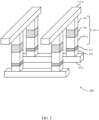
- FIG. 2 illustrates an example memory array 200 that supports chalcogenide memory device components and compositions in accordance with various embodiments of the present disclosure.
- Memory array 200 may be an example of memory array 100 described with reference to FIG. 1 .
- Memory array 200 includes memory cell 105-a, first access line 110-a (e.g. word line 1 10-a), and second access line 115-a (e.g. bit line 115-a), which may be examples of a memory cell 105, word line 110, and bit line 115, as described with reference to FIG. 1 .
- Memory cell 105-a includes electrode 205, electrode 205-a, and memory element 220, which may be a ferroelectric material. Electrode 205-a of memory cell 105-a may be referred to as middle electrode 205-a.
- Memory array 200 may also include bottom electrode 210 and selector device 215, which may also be referred to as a selection component.
- a three-dimensional (3D) memory array may be formed by stacking multiple memory arrays 200 on one another.
- the two stacked arrays may, in some examples, have common conductive lines such that each level may share word lines 110 or bit lines 115 as described with reference to FIG. 1 .
- Memory cell 105-a may be a target memory cell.
- Memory array 200 may be referred to as a cross-point architecture. It may also be referred to as a pillar structure.
- a pillar may be in contact with a first conductive line (first access line 110-a) and a second conductive line (second access line 115-a), where the pillar comprises a first electrode (bottom electrode 210), selector device 215, and ferroelectric memory cell 105-a, where ferroelectric memory cell 105-a includes a second electrode (electrode 205-a), memory element 220, and a third electrode (electrode 205).
- electrode 205-a may be referred to as a middle electrode.
- first access line 110-a may be in electronic communication with the second access line 115-a via the memory cell 105-a.
- First access line 110-a and second access line 115-a may be arranged in a three-dimensional cross-point configuration and may be in electronic communication with the plurality of memory cells 105-a.
- Such a pillar architecture may offer relatively high-density data storage with lower production costs compared to other memory architectures.
- the cross-point architecture may have memory cells with a reduced area and, resultantly, an increased memory cell density compared to other architectures.
- the architecture may have a 4F 2 memory cell area, where F is the smallest feature size, compared to other architectures with a 6F 2 memory cell area, such as those with a three-terminal selection.
- DRAM may use a transistor, which is a three-terminal device, as the selection component for each memory cell and may have a larger memory cell area compared to the pillar architecture.
- Selector device 215 may, in some cases, be connected in series between a memory cell 105 and a conductive line, for example, between memory cell 105-a and at least one of first access line 110-a or second access line 115-a.
- selector device 215 may be located between electrode 205-a and bottom electrode 210; thus, selector device 215 is located in series between memory cell 105-a and first access line 110-a.
- selector device 215 may be located in series between memory cell 105-a and second access line 115-a.
- the selection component may aid in selecting a particular memory cell 105-a or may help prevent stray currents from flowing through non-selected memory cells 105-a adjacent a selected memory cell 105-a.
- selector device 215 may have a threshold voltage such that a current flows through selector device 215 when the threshold voltage is met or exceeded.
- Selector device 215 may be coupled with the memory element 220.
- the selector device 215 and the memory element 220 may be arranged in a series configuration between the first access line 110-a and the second access line 115-a.
- a selector device 215 may include a first chalcogenide material comprising a composition of Se, As, and at least one of B, Al, Ga, In, and Tl.
- a selector device 215 may include a first chalcogenide material comprising a composition of Se, Ge, and at least one of B, Al, Ga, In, and Tl.
- a selector device 215 may include a first chalcogenide material excluding As.
- a selector device 215 may comprise a first chalcogenide material and a memory element 220 may comprise a different composition (e.g., a second chalcogenide material) than the selector device 215.
- a cell 105 may not use a separate memory element and selector device.
- This type of memory architecture may be referred to as self-selecting memory (SSM), and the selector device 215 may serve as the memory storage element.
- a memory device may therefore include a memory cell that comprises a self-selecting memory component (e.g., self-selecting memory cell).
- the self-selecting memory cell may comprise a chalcogenide material composition as described herein.
- the self-selecting memory component may include a selection capability (e.g., function as the selector device) and a storage capability (e.g., function as the storage component).
- a selection capability e.g., function as the selector device
- a storage capability e.g., function as the storage component
- a single element (component) that includes a chalcogenide material may serve as both a memory element and a selector device such that a separate selector device may be unncessary.
- the memory element 220 may comprise a ferroelectric capacitor, a linear capacitor, or a memristor rather than a phase change material, or may comprise a chalcogenide material composition as described herein.
- the memory element 220 may be configured to store data.
- the selector device 215 may be configured to store additional data (e.g., in addition to data stored by one or more memory elements 220 also included in the memory cell 105).
- Selector device 215 may be separated from memory element 220 by middle electrode 205-a.
- middle electrode 205-a may electrically float-that is, charge may accumulate because it may not be directly connected to an electrical ground or a component capable of being electrically grounded.
- Memory element 220 may be accessed via selector device 215. For example, when a voltage across selector device 215 reaches a threshold value, current may flow between access lines 110-a and 115-a through memory element 220. This flow of current may be used to read a logic value stored at memory element 220.
- the threshold voltage across selector device 215 at which current begins to flow may be a function of the composition of selector device 215. Likewise, the composition of selector device 215 may affect whether and the extent to which the threshold voltage of selector device 215 may change over time.
- Threshold voltage drift may be undesirable because as the threshold voltage of a selector device changes, the operation (e.g., the application of voltage necessary to cause current to flow through the selector device) may change. This may complicate reading or writing of the device, may lead to inaccurate reading or writing, may cause increases in power necessary to read or write to a memory element, and the like. So as described herein, employing compositions of matter for selector device 215 that limit the likelihood or extent of threshold voltage drift may serve to improve device performance. Selector device 215 may thus comprise a composition that includes one or more Group III elements, which, as discussed below, may limit threshold voltage drift.
- a memory window for a chalcogenide material or a memory cell that includes a chalcogenide material as a storage element may correspond to a difference in threshold voltage for the chalcogenide material compositions when programmed using voltages of opposite polarities.
- a chalcogenide material composition may be programmed using a positive polarity, thereby resulting in the chalcogenide material composition having a first threshold voltage.
- the chalcogenide material composition may additionally or alternatively be programmed using a negative polarity, thereby resulting in the chalcogenide material composition having a second threshold voltage that is different than the first threshold voltage.
- the difference between the first threshold voltage and the second threshold voltage may be referred to as the memory window.
- the memory window of a chalcogenide material composition may be influenced by the aggregate or combined amount of Germanium and at least one Group III element (e.g., In), as may the standard deviation of the threshold voltages. For example, increasing the aggregate or combined amount of Germanium and the at least one Group III element may increase the memory window and decrease the standard deviation of the threshold voltages.
- employing compositions of chalcogenide material for selector device 215, memory element 220, or a self-selecting memory element may increase the memory window, decrease the standard deviation of the threshold voltage, or both, which may improve device performance.
- a memory cell 105 that comprises at least one chalcogenide material that includes one or more Group III elements (e.g., In) as described herein, and which may in some cases exclude As, thus may support improved memory performance along with other benefits (e.g., ease, cost, or safety of manufacture).
- Group III elements e.g., In
- Memory array 200 may be made by various combinations of material formation and removal. For example, layers of material may be deposited that correspond to the first access line110-a, bottom electrode 210, selector device 215, electrode 205-a, memory element 220, and electrode 205. Material may be selectively removed to then create the desired features, such as the pillar structure depicted in FIG. 2 . For example, features may be defined using photolithography to pattern a photoresist and then material may be removed by techniques such as etching. Second access lines 115-a may then be formed, for example, by depositing a layer of material and selectively etching to form the line structure depicted in FIG. 2 . In some cases, electrically insulating regions or layers may be formed or deposited. The electrically insulating regions may include oxide or nitride materials, such as silicon oxide, silicon nitride, or other electrically insulating materials.
- CVD chemical vapor deposition
- MOCVD metal-organic chemical vapor deposition
- PVD physical vapor deposition
- ALD atomic layer deposition
- MBE molecular beam epitaxy
- FIG. 3 illustrates a plot 300 of characteristics of chalcogenide memory device components and compositions in accordance with embodiments of the present disclosure. As described herein, FIG. 3 depicts a comparison of chalcogenide material compositions, including a composition that includes a Group III element. FIG. 3 thus illustrates the relatively lower voltage drift of a composition of Se, As, and a Group III element, which is depicted as composition 3 (Comp. 3).
- composition 3 may be approximately 53% Se by weight, approximately 23% As by weight, approximately 13% Ge by weight, and approximately 11% In by weight, relative to the total weight of the composition.
- Composition 3 at point 305 may have a voltage drift of less than 250 millivolts after 3 days at 90 degrees Celsius.
- compositions 1 and 2 may be pure SAG compositions (i.e. including only Se, As, Ge).
- Compositions 4 and 5 may be pure Si-SAG alloys (i.e. including only Se, As, Ge, Si).
- compositions 4 and 5 may have the amount of approximately 30% As by weight, approximately 12% Ge by weight, and approximately 8% Si by weight, relative to the total weight of the composition.
- the chalcogenide material compositions i.e. composition 1 at point 310, composition 2 at point 315, composition 4 at point 320, composition 5 at point 325) may drift more than 500 millivolts after 3 days at 90 degrees Celsius.
- a chalcogenide material composition (e.g. composition 3) may yield results identified in TABLE 1.
- Table 1 Vth_FF [V] Vth_SF [V] Vform [V] Vth_1000 [V] I @ 0.85 Vt (@ 1e3) [nA] STDrift [mV/dec] WT ⁇ 1 s 5.00 4.77 0.06 4.25 35 0
- the Vth_FF and Vth_SF column headings may represent the threshold voltage read at the first activation (i.e., a "first fire") and a subsequent activation (i.e., "second fire") of a selector device having composition 3, respectively.
- the Vform column heading may represent the threshold voltage difference between the first fire and the second fire.
- the Vth _1000 column heading may represent the threshold voltage after 1000 cycles.
- the I @ 0.84 Vt column heading may represent the sub threshold voltage leakage current in the selector device.
- the STDrift column heading may represent the drift of the selector device. So as shown in Table 3, a chalcogenide composition that include In or another Group III element (e.g. composition 3) may result in stable threshold voltages during cycling and a low drift over a period of time.
- FIG. 4 illustrates a plot 400 of characteristics of chalcogenide memory device components and compositions in accordance with embodiments of the present disclosure.
- region 405 illustrates compositions of Se, As, and Ge that may be doped with a Group III element.
- Dotted line 410 illustrates the As 2 Se 3 -GeSe 2 composition line.
- compositions with low voltage drift may be useful for selector devices or other memory elements and may include some combination of Se, As, Ge, Si, or Group III elements.
- a chalcogenide material composition may result in the general formula Se x As y Ge z Si w X u , where X is one of the Group III elements.
- a chalcogenide material composition may result in the formula Se 4 As 2 GeSiIn, where In is one of the Group III elements.
- a chalcogenide material composition may result in the formula Se 3 As 2 GeSi 2 B, where B is one of the Group III elements.
- Chalcogenide material compositions may be comprised of the compositions identified in TABLE 2, which may provide composition ranges by weight percentages of Se, As, Ge, Si, and a Group III element. Table 2 Se As Ge Si group III element First (%) >40 10-35 1-20 1-15 0.15-35 Second (%) >45 12-32 1-20 1-15 0.15-24
- Se may be in an amount greater than or equal to 40% by weight, relative to a total weight of the composition. In some cases, the amount of Se may be greater than or equal to 45% by weight, relative to the total weight of the composition.
- Arsenic may be in an amount ranging from 10% to 35% by weight, relative to the total weight of the composition. In some cases, the amount of As ranges from 12% to 32% by weight, relative to the total weight of the composition.
- Ge may be in an amount ranging from 1% to 20% by weight, relative to the total weight of the composition.
- Si may be in an amount ranging from 1% to 15% by weight, relative to the total weight of the composition.
- the combination of Si, Ge, and at least one element selected from the group consisting of B, Al, Ga, In, and Tl may be an amount greater than or equal to 20% by weight, relative to the total weight of the composition.
- a Group III element may be at least one element selected from a group consisting of B, Al, Ga, In, and Tl in an amount ranging from 0.15% to 35% by weight, relative to the total weight of the composition. In some cases, the at least one element selected from the group consisting of B, Al, Ga, In, and TI in an amount ranging from 0.15% to 24% by weight, relative to the total weight of the composition.
- the chalcogenide material compositions of TABLE 2 may have a threshold voltage drift of less than or equal to 250 millivolts after three days at a temperature of 90 degrees Celsius.
- the chalcogenide material compositions of TABLE 2 may have the glass transition temperature greater than 280 degrees Celsius. Glass transition temperature and glass processing conditions may have an impact upon a composition selection within the ranges provided by TABLE 2.
- a Group III element may be incorporated into a composition of matter, such as a composition of Se and As or SAG or Si-SAG to mitigate various problems associated with the selector device have pure SAG or Si-SAG compositions.
- too little Ge may compromise the thermal stability of the chalcogenide material composition.
- a SAG system with a Ge composition greater than 15% may be too thermally unstable to be integrated into cross-point arrays.
- a high composition of Se may result in a high band gap energy that may sustain a high threshold voltage and leakage trade off.
- a Group III element may increase selector device stability through the formation of strong and stable bonds.
- Group III elements may form tetrahedral bonds that may not degrade drift.
- a lower voltage drift, as depicted in FIG. 3 may be directly related to the bond structure.
- the Al-Se bond dissociation energy may be 318 kJ mol-1
- the In-Se bond dissociation energy may be 245 kJ mol-1.
- a higher bond dissociation energy may correlate to a stronger and more stable bond.
- a Group III element may also provide increased thermal stability in the selector device.
- Al 2 Se 3 may have a band gap energy of 3.1 eV, and In 2 Se 3 may have a band gap energy of 2.1 eV.
- a wider band gap may increase the threshold voltage over time and may allow the selector device to operate at higher temperatures.
- Al 2 Se 3 may have a melting temperature of 1220 K, and In 2 Se 3 may have a melting temperature of 933 K.
- a high melting temperature may increase the thermal stability of the selector device.
- the transition temperature of the chalcogenide material composition may also increase.
- the addition of a Group III element to chalcogenide material composition in the selector device may provide additional benefits.
- the introduction of B into a selector device may serve as an insulator. Therefore, a selector device comprising a B-SAG system may prevent leakage issues.
- introduction of Al may facilitate integration into cross-point arrays.
- introduction of In may minimize voltage drift.
- Introduction of a group III element (e.g. B, Al, Ga, In, Tl) into the chalcogenide material composition may increase selector device stability.
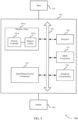
- FIG. 5 illustrates a system 500, including a memory array, that supports or employs chalcogenide memory device components in accordance with embodiments of the present disclosure.
- System 500 may include a device 505, which may be or include a printed circuit board to connect or physically support various components.
- Device 505 may include a memory array 100-a, which may be an example of memory array 100 described in FIG. 1 .
- Memory array 100-a may contain memory controller 140-a and memory cell(s) 105-b, which may be examples of memory controller 140 described with reference to FIG. 1 and memory cells 105 described with reference to FIGs. 1 and 2 .
- Memory array 100-a may include a plurality of memory cells 105-a each having a memory element and a selector device, and each selector device may comprise a chalcogenide material having a composition of selenium, arsenic, and at least one of boron, aluminum, gallium, indium, or thallium.
- the composition of the chalcogenide material comprises germanium or silicon, or both.
- composition of the chalcogenide material comprises a combination of the silicon, the germanium, and the at least one of the boron, aluminum, gallium, indium, or thallium in an amount greater than or equal to 20% by weight, relative to a total weight of the composition.
- Memory array 100-a may also include a plurality of access lines arranged in a three-dimensional cross-point configuration and in electronic communication with the plurality of memory cells 105-a.
- Device 505 may also include a processor 510, BIOS component 515, peripheral component(s) 520, and input/output control component 525.
- the components of device 505 may be in electronic communication with one another through bus 530.
- Processor 510 may be configured to operate memory array 100-a through memory controller 140-a. In some cases, processor 510 performs the functions of memory controller 140 described with reference to FIGs. 1 . In other cases, memory controller 140-a may be integrated into processor 510. Processor 510 may be a general-purpose processor, a digital signal processor (DSP), an application-specific integrated circuit (ASIC), a field-programmable gate array (FPGA) or other programmable logic device, discrete gate or transistor logic, discrete hardware components, or it may be a combination of these types of components, and processor 510 may perform various functions described herein. Processor 510 may, for example, be configured to execute computer-readable instructions stored in memory array 100-a to cause device 505 perform various functions or tasks.
- DSP digital signal processor
- ASIC application-specific integrated circuit
- FPGA field-programmable gate array
- BIOS component 515 may be a software component that includes a basic input/output system (BIOS) operated as firmware, which may initialize and run various hardware components of system 500. BIOS component 515 may also manage data flow between processor 510 and the various components, e.g., peripheral components 520, input/output control component 525, etc. BIOS component 515 may include a program or software stored in read-only memory (ROM), flash memory, or any other non-volatile memory.
- BIOS basic input/output system
- BIOS component 515 may include a program or software stored in read-only memory (ROM), flash memory, or any other non-volatile memory.
- Peripheral component(s) 520 may be any input or output device, or an interface for such devices, that is integrated into device 505. Examples may include disk controllers, sound controller, graphics controller, Ethernet controller, modem, universal serial bus (USB) controller, a serial or parallel port, or peripheral card slots, such as peripheral component interconnect (PCI) or accelerated graphics port (AGP) slots.
- PCI peripheral component interconnect
- AGP accelerated graphics port
- Input/output control component 525 may manage data communication between processor 510 and peripheral component(s) 520, input 535 devices, or output 540 devices. Input/output control component 525 may also manage peripherals not integrated into device 505. In some cases, input/output control component 525 may represent a physical connection or port to the external peripheral.
- Input 535 may represent a device or signal external to device 505 that provides input to device 505 or its components. This may include a user interface or interface with or between other devices. In some cases, input 535 may be a peripheral that interfaces with device 505 via peripheral component(s) 520 or may be managed by input/output control component 525.
- Output 540 may represent a device or signal external to device 505 configured to receive output from device 505 or any of its components. Examples of output 540 may include data or signals sent to a display, audio speakers, a printing device, another processor or printed circuit board, etc. In some cases, output 540 may be a peripheral that interfaces with device 505 via peripheral component(s) 520 or may be managed by input/output control component 525.
- the components of memory controller 140-a, device 505, and memory array 100-a may be made up of circuitry designed to carry out their functions. This may include various circuit elements, for example, conductive lines, transistors, capacitors, inductors, resistors, amplifiers, or other active or inactive elements, configured to carry out the functions described herein.
- FIG. 6 illustrates a plot 600 of characteristics of chalcogenide memory device components and compositions in accordance with embodiments of the present disclosure.
- plot 600 represents aspects of a ternary Ge-As-Se plan
- compositions corresponding to plot 600 may additionally include a Group III element (including at least one element selected from a group consisting of B, Al, Ga, In, and Tl).
- region 605 illustrates compositions of Se and Ge (and potentially also As) that may be doped with a Group III element.
- Region 610 illustrates additional compositions of Se and Ge (and potentially also As) that may be doped with a Group III element.
- region 610 may include region 615 that may illustrate compositions of Se, Ge, and a Group III element without As.
- compositions with an increased memory window and low standard deviation of the threshold voltage may be useful for selector devices or other memory elements and may include some combination of Se, As, Ge, or Group III elements.
- Chalcogenide material compositions may be comprised of the compositions identified in TABLE 3, which may provide composition ranges by atomic percentages (at.%) of Se, As, Ge, and a Group III element. Table 3 Se As Ge Group III element First (at.%) ⁇ 40 ⁇ 30 8-35 1-15 Second (at.%) ⁇ 40 ⁇ 1 8-35 1-15 Third (at.%) ⁇ 40 0 8-35 1-15 Fourth (at.%) ⁇ 40 ⁇ 30 (e.g., ⁇ 1, or 0) 20-35 1-15
- Se may be in an amount greater than or equal to 40 at.% of the chalcogenide material.
- Arsenic may be in an amount less than or equal to 30 at.% of the chalcogenide material.
- the amount of As may be in an amount less than or equal to 1 at.% of the chalcogenide material (or otherwise in a trace or de minimis amount).
- the composition may include no As.
- Ge may be in an amount ranging from 8 at.% to 35 at.% of the chalcogenide material, which in some cases may substantially correspond to region 605. In other examples, the amount of Ge may be in an amount ranging from 20 at.% to 35 at.% of the chalcogenide material, which in some cases may substantially correspond to region 610.
- a Group III element may be at least one element selected from a group consisting of B, Al, Ga, In, and Tl in an amount ranging from 1 at.% to 15 at.% of the chalcogenide material (inclusive).
- the at least one element selected from the group may consist of In in an amount ranging from 1 at.% to 15 at.% of the chalcogenide material.
- the at least one element selected from the group may consist of B in an amount ranging from 1 at.% to 15 at.% of the chalcogenide material.
- the at least one element selected from the group may consist of Al in an amount ranging from 1 at.% to 15 at.% of the chalcogenide material. In some cases, the at least one element selected from the group may consist of Ga in an amount ranging from 1 at.% to 15 at.% of the chalcogenide material. In some cases, the at least one element selected from the group may consist of TI in an amount ranging from 1 at.% to 15 at.% of the chalcogenide material.
- Chalcogenide material compositions may be comprised of the compositions identified in TABLE 4, which may provide composition ranges by atomic percentages (at.%) of Se, As, Ge, and a Group III element.
- region 605 and region 610 may represent chalcogenide compositions identified in TABLE 4.
- Table 4 Se As Ge Group III element First (at.%) ⁇ 40 ⁇ 40 8-35 1-15 Second (at.%) ⁇ 40 ⁇ 40 (e.g., ⁇ 30, ⁇ 1, or 0) 8-35 1-15
- Se may be in an amount greater than or equal to 40 at.% of the chalcogenide material.
- Arsenic may be in an amount less than or equal to 40 at.% of the chalcogenide material. In some cases, As may be in an amount less than or equal to 30 at.% of the chalcogenide material, As may be an in amount less than or equal to 1 at.% of the chalcogenide material, or there may be no amount of As in the chalcogenide material.
- Ge may be in an amount ranging from 8 at.% to 35 at.% of the chalcogenide material. In some cases, the presence of Ge may affect the threshold voltage drift.
- a Group III element may be at least one element selected from a group consisting of B, Al, Ga, In, and Tl in an amount ranging from 1 at.% to 15 at.% of the composition.
- Chalcogenide material compositions may be comprised of the compositions identified in TABLE 5, which may provide composition ranges by atomic percentages (at.%) of Se, As, Ge, and a Group III element.
- region 610 may represent chalcogenide compositions identified in TABLE 5.
- Table 5 Se As Ge Group III element First (at.%) ⁇ 40 ⁇ 30 20-35 1-15 Second (at.%) ⁇ 40 ⁇ 40 (e.g., ⁇ 30, ⁇ 1, or 0) 20-35 1-15
- Se may be in an amount greater than or equal to 40 at.% of the chalcogenide material.
- Arsenic may be in an amount less than or equal to 30 at.% of the chalcogenide material. In some cases, As may be in an amount less than or equal to 40 at.% of the chalcogenide material, As may be an in amount less than or equal to 1 at.% of the chalcogenide material, or there may be no amount of As in the chalcogenide material.
- Ge may be in an amount ranging from 20 at.% to 35 at.% of the chalcogenide material.
- a Group III element may be at least one element selected from a group consisting of B, Al, Ga, In, and Tl in an amount ranging from 1 at.% to 15 at.% of the chalcogenide material.
- region 615 may represent chalcogenide compositions without As.
- Excluding As from the chalcogenide material composition may provide value to the memory device regarding safety costs (e.g., in-line handling control, selector device manufacturer availability, and environmental impact).
- safety costs e.g., in-line handling control, selector device manufacturer availability, and environmental impact.
- the absence of As in the chalcogenide material may decrease the complexity of the composition, thereby simplifying the chemical deposition process.
- Compositions that may include Se, Ge, and a Group III element without As may also enhance the integration of the chalcogenide material composition in cross point technology developments (e.g., three-dimensional cross point architectures, ReRAM, DRAM, RAM, or the like), thereby enabling ALD deposition.
- the chalcogenide material composition excluding As may be detected using transmission electron microscopy (TEM), electron dispersion x-ray spectroscopy (EDX), or both.
- TEM transmission electron microscopy
- EDX electron dispersion x-ray spectroscopy
- FIG. 7 illustrates a plot 700 of characteristics of chalcogenide memory device components and compositions in accordance with embodiments of the present disclosure.
- plot 700 illustrates compositions of Se and Ge that may be doped with a Group III element (e.g., In).
- the plot 700 including region 705, illustrates compositions of chalcogenide materials without As (e.g., As-free compositions) and may, for example, correspond to compositions included in plot 600 along the Se-Ge tie line (e.g., including region 615).
- a chalcogenide material composition may result in the general formula Se x As y Ge z X u , where X is one of the Group III elements.
- a chalcogenide material composition may result in the formula GeSe 3 , GeSe 2 , GeSe, or In 2 Se 3 , where In is one of the Group III elements.
- a Group III element may be incorporated into a composition of matter, such as a composition of Se and Ge or SAG to mitigate various problems associated with memory elements that may have pure SAG or Se and Ge compositions.
- In may be incorporated into a composition of matter containing Se and Ge.
- the memory window may increase as the amount of In and Ge increases within the composition of matter.
- the memory window may decrease as the amount of In and Ge increases within the composition of matter.
- an increase in the memory window may increase the memory elements' thickness scalability.
- region 705 may represent compositions without As. In such cases, the absence of As may not affect the memory window.
- a composition as depicted by region 705 with no As (or little As) may have a memory window that is little changed relative to a composition that includes As (e.g., a memory window that is identical to a composition that includes As, substantially identical to a composition that includes As, or at least operationally viable for a memory device).
- FIG. 8 illustrates a system 800, including a memory array, that supports or employs chalcogenide memory device components in accordance with embodiments of the present disclosure.
- System 800 may include a device 805, which may be or include a printed circuit board to connect or physically support various components.
- Device 805 may include a memory array 100-b, which may be an example of memory array 100 described in FIG. 1 .
- Memory array 100-b may contain memory controller 140-b and memory cell(s) 105-c, which may be examples of memory controller 140 described with reference to FIG. 1 and memory cells 105 described with reference to FIGs. 1 and 2 .
- Memory array 100-b may include a plurality of memory cells 105-b each comprising (e.g., as at least one of a selector device, a memory element, or a self-selecting memory element) a chalcogenide material having a composition of selenium, germanium, and at least one of boron, aluminum, gallium, indium, or thallium.
- the composition of the chalcogenide material comprises arsenic.
- composition of the chalcogenide material comprises selenium in an amount greater than or equal to 40 at.% of the composition, germanium in an amount ranging from 8 at.% to 35 at.% of the composition, and at least one element selected from a group consisting of boron, aluminum, gallium, indium, and thallium in an amount ranging from 1 at.% to 15 at.% of the composition.
- Memory array 100-b may also include a plurality of access lines arranged in a three-dimensional cross-point configuration and in electronic communication with the plurality of memory cells 105-b.
- Device 805 may also include a processor 810, BIOS component 815, peripheral component(s) 820, and input/output control component 825.
- the components of device 805 may be in electronic communication with one another through bus 830.
- Processor 810 may be configured to operate memory array 100-b through memory controller 140-b. In some cases, processor 810 performs the functions of memory controller 140 described with reference to FIGs. 1 . In other cases, memory controller 140-b may be integrated into processor 810.
- Processor 810 may be a general-purpose processor, a digital signal processor (DSP), an application-specific integrated circuit (ASIC), a field-programmable gate array (FPGA) or other programmable logic device, discrete gate or transistor logic, discrete hardware components, or it may be a combination of these types of components, and processor 810 may perform various functions described herein.
- Processor 810 may, for example, be configured to execute computer-readable instructions stored in memory array 100-b to cause device 805 perform various functions or tasks.
- BIOS component 815 may be a software component that includes a basic input/output system (BIOS) operated as firmware, which may initialize and run various hardware components of system 800. BIOS component 815 may also manage data flow between processor 810 and the various components, e.g., peripheral components 820, input/output control component 825, etc. BIOS component 815 may include a program or software stored in read-only memory (ROM), flash memory, or any other non-volatile memory.
- BIOS basic input/output system
- BIOS component 815 may include a program or software stored in read-only memory (ROM), flash memory, or any other non-volatile memory.
- Peripheral component(s) 820 may be any input or output device, or an interface for such devices, that is integrated into device 805. Examples may include disk controllers, sound controller, graphics controller, Ethernet controller, modem, universal serial bus (USB) controller, a serial or parallel port, or peripheral card slots, such as peripheral component interconnect (PCI) or accelerated graphics port (AGP) slots.
- PCI peripheral component interconnect
- AGP accelerated graphics port
- Input/output control component 825 may manage data communication between processor 810 and peripheral component(s) 820, input 835 devices, or output 840 devices. Input/output control component 825 may also manage peripherals not integrated into device 805. In some cases, input/output control component 825 may represent a physical connection or port to the external peripheral.
- Input 835 may represent a device or signal external to device 805 that provides input to device 805 or its components. This may include a user interface or interface with or between other devices. In some cases, input 835 may be a peripheral that interfaces with device 805 via peripheral component(s) 820 or may be managed by input/output control component 825.
- Output 840 may represent a device or signal external to device 805 configured to receive output from device 805 or any of its components. Examples of output 840 may include data or signals sent to a display, audio speakers, a printing device, another processor or printed circuit board, etc. In some cases, output 840 may be a peripheral that interfaces with device 805 via peripheral component(s) 820 or may be managed by input/output control component 825.
- memory controller 140-b, device 805, and memory array 100-b may be made up of circuitry designed to carry out their functions. This may include various circuit elements, for example, conductive lines, transistors, capacitors, inductors, resistors, amplifiers, or other active or inactive elements, configured to carry out the functions described herein.
- selector device selector component, and selector element
- memory element memory component, storage device, storage component, and storage element
- self-selecting memory element and self-selecting memory component may be used interchangeably.
- 'coupled to' indicates components that are substantially in contact with one another.
- two components may be coupled even if a third material or component physically separates them.
- This third component may not substantially alter the two components or their functions. Instead, this third component may aid or enable the connection of the first two components.
- some materials may not strongly adhere when deposited on a substrate material.
- Thin (e.g., on the order of a few nanometers or less) layers, such as lamina layers, may be used between two materials to enhance their formation or connection.
- a third material may act as a buffer to chemically isolate two components.
- each layer may have three dimensions (e.g., height, width, and depth) and may cover some or all of a surface.
- a layer may be a three-dimensional structure where two dimensions are greater than a third, e.g., a thin-film.
- Layers may include different elements, components, and/or materials.
- one layer may be composed of two or more sublayers.
- two dimensions of a three-dimensional layer are depicted for purposes of illustration. Those skilled in the art will, however, recognize that the layers are three-dimensional in nature
- the term “substantially” means that the modified characteristic (e.g., a verb or adjective modified by the term substantially) need not be absolute but is close enough so as to achieve the advantages of the characteristic.
- Electrode may refer to an electrical conductor, and in some cases, may be employed as an electrical contact to a memory cell or other component of a memory array.
- An electrode may include a trace, wire, conductive line, conductive layer, or the like that provides a conductive path between elements or components of memory array 100.
- photolithography may refer to the process of patterning using photoresist materials and exposing such materials using electromagnetic radiation.
- a photoresist material may be formed on a base material by, for example, spin-coating the photoresist on the base material.
- a pattern may be created in the photoresist by exposing the photoresist to radiation.
- the pattern may be defined by, for example, a photo mask that spatially delineates where the radiation exposes the photoresist. Exposed photoresist areas may then be removed, for example, by chemical treatment, leaving behind the desired pattern. In some cases, the exposed regions may remain and the unexposed regions may be removed.
- the term "electronic communication” refers to a relationship between components that supports electron flow between the components. This may include a direct connection between components or may include intermediate components. Components in electronic communication may be actively exchanging elections or signals (e.g., in an energized circuit) or may not be actively exchanging electrons or signals (e.g., in a de-energized circuit) but may be configured and operable to exchange electrons or signals upon a circuit being energized. By way of example, two components physically connected via a switch (e.g., a transistor) are in electronic communication regardless of the state of the switch (i.e., open or closed).
- a switch e.g., a transistor
- the devices discussed herein, including memory array 100 may be formed on a semiconductor substrate, such as silicon (Si), germanium, silicon-germanium alloy, gallium arsenide (GaAs), gallium nitride (GaN), etc.
- the substrate is a semiconductor wafer.
- the substrate may be a silicon-on-insulator (SOI) substrate, such as silicon-on-glass (SOG) or silicon-on-sapphire (SOP), or epitaxial layers of semiconductor materials on another substrate.
- SOI silicon-on-insulator
- SOG silicon-on-glass
- SOP silicon-on-sapphire
- the conductivity of the substrate, or sub-regions of the substrate may be controlled through doping using various chemical species including, but not limited to, phosphorous, boron, or arsenic. Doping may be performed during the initial formation or growth of the substrate, by ion-implantation, or by any other doping means.
- Chalcogenide materials may be materials or alloys that include at least one of the elements S, Se, and Te. Phase change materials discussed herein may be chalcogenide materials. Chalcogenide materials may include alloys of S, Se, Te, Ge, As, Al, Sb, Au, indium (In), gallium (Ga), tin (Sn), bismuth (Bi), palladium (Pd), cobalt (Co), oxygen (O), silver (Ag), nickel (Ni), platinum (Pt).
- Example chalcogenide materials and alloys may include, but are not limited to, Ge-Te, In-Se, Sb-Te, Ga-Sb, In-Sb, As-Te, Al-Te, Ge-Sb-Te, Te-Ge-As, In-Sb-Te, Te-Sn-Se, Ge-Se-Ga, Bi-Se-Sb, Ga-Se-Te, Sn-Sb-Te, In-Sb-Ge, Te-Ge-Sb-S, Te-Ge-Sn-O, Te-Ge-Sn-Au, Pd-Te-Ge-Sn, In-Se-Ti-Co, Ge-Sb-Te-Pd, Ge-Sb-Te-Co, Sb-Te-Bi-Se, Ag-In-Sb-Te, Ge-Sb-Se-Te, Ge-Sn-Sb-Te, Ge-Te-N-S
- the hyphenated chemical composition notation indicates the elements included in a particular compound or alloy and is intended to represent all stoichiometries involving the indicated elements.
- Ge-Te may include Ge x Te y , where x and y may be any positive integer.
- Other examples of variable resistance materials may include binary metal oxide materials or mixed valence oxide including two or more metals, e.g., transition metals, alkaline earth metals, and/or rare earth metals. Embodiments are not limited to a particular variable resistance material or materials associated with the memory elements of the memory cells.
- other examples of variable resistance materials can be used to form memory elements and may include chalcogenide materials, colossal magnetoresistive materials, or polymer-based materials, among others.
- Transistors discussed herein may represent a field-effect transistor (FET) and comprise a three terminal device including a source, drain, and gate.
- the terminals may be connected to other electronic elements through conductive materials, e.g., metals.
- the source and drain may be conductive and may comprise a heavily-doped, e.g., degenerate, semiconductor region.
- the source and drain may be separated by a lightly-doped semiconductor region or channel. If the channel is n-type (i.e., majority carriers are electrons), then the FET may be referred to as an n-type FET. Likewise, if the channel is p-type (i.e., majority carriers are holes), then the FET may be referred to as a p-type FET.
- the channel may be capped by an insulating gate oxide.
- the channel conductivity may be controlled by applying a voltage to the gate. For example, applying a positive voltage or negative voltage to an n-type FET or a p-type FET, respectively, may result in the channel becoming conductive.
- a transistor may be "on” or “activated” when a voltage greater than or equal to the transistor's threshold voltage is applied to the transistor gate. The transistor may be “off” or “deactivated” when a voltage less than the transistor's threshold voltage is applied to the transistor gate.
- a general-purpose processor may be a microprocessor, but in the alternative, the processor may be any conventional processor, controller, microcontroller, or state machine.
- a processor may also be implemented as a combination of computing devices (e.g., a combination of a DSP and a microprocessor, multiple microprocessors, one or more microprocessors in conjunction with a DSP core, or any other such configuration).
- the functions described herein may be implemented in hardware, software executed by a processor, firmware, or any combination thereof. If implemented in software executed by a processor, the functions may be stored on or transmitted over as one or more instructions or code on a computer-readable medium. Other examples and implementations are within the scope of the disclosure and appended claims. For example, due to the nature of software, functions described above can be implemented using software executed by a processor, hardware, firmware, hardwiring, or combinations of any of these. Features implementing functions may also be physically located at various positions, including being distributed such that portions of functions are implemented at different physical locations.
- Computer-readable media includes both non-transitory computer storage media and communication media including any medium that facilitates transfer of a computer program from one place to another.
- a non-transitory storage medium may be any available medium that can be accessed by a general purpose or special purpose computer.
- non-transitory computer-readable media can comprise RAM, ROM, electrically erasable programmable read only memory (EEPROM), compact disk (CD) ROM or other optical disk storage, magnetic disk storage or other magnetic storage devices, or any other non-transitory medium that can be used to carry or store desired program code means in the form of instructions or data structures and that can be accessed by a general-purpose or special-purpose computer, or a general-purpose or special-purpose processor.
- RAM random access memory
- ROM read only memory
- EEPROM electrically erasable programmable read only memory
- CD compact disk
- magnetic disk storage or other magnetic storage devices or any other non-transitory medium that can be used to carry or store desired program code means in the form of instructions or data structures
- any connection is properly termed a computer-readable medium.
- the software is transmitted from a website, server, or other remote source using a coaxial cable, fiber optic cable, twisted pair, digital subscriber line (DSL), or wireless technologies such as infrared, radio, and microwave
- the coaxial cable, fiber optic cable, twisted pair, digital subscriber line (DSL), or wireless technologies such as infrared, radio, and microwave are included in the definition of medium.
- Disk and disc include CD, laser disc, optical disc, digital versatile disc (DVD), floppy disk and Blu-ray disc where disks usually reproduce data magnetically, while discs reproduce data optically with lasers. Combinations of the above are also included within the scope of computer-readable media.
Landscapes
- Chemical & Material Sciences (AREA)
- Crystallography & Structural Chemistry (AREA)
- Life Sciences & Earth Sciences (AREA)
- Engineering & Computer Science (AREA)
- Chemical Kinetics & Catalysis (AREA)
- General Chemical & Material Sciences (AREA)
- Geochemistry & Mineralogy (AREA)
- Materials Engineering (AREA)
- Organic Chemistry (AREA)
- Semiconductor Memories (AREA)
- Glass Compositions (AREA)
Abstract
Description
- The present Application for Patent claims priority to
Singapore Patent Application 10201810518W by Fantini et al., entitled "Chalcogenide Memory Device Components and Composition," filed November 26, 2018 U.S. Patent Application No. 16/228,469 by Fantini et al., entitled "Chalcogenide Memory Device Components and Composition," filed December 20, 2018 - The following relates generally to memory devices and more specifically to chalcogenide memory device components and chemistry.
- Memory devices are widely used to store information in various electronic devices such as computers, wireless communication devices, cameras, digital displays, and the like. Information is stored by programing different states of a memory device. For example, binary devices have two states, often denoted by a logic "1" or a logic "0." In other systems, more than two states may be stored. To access the stored information, a component of the electronic device may read, or sense, the stored state in the memory device. To store information, a component of the electronic device may write, or program, the state in the memory device.
- Multiple types of memory devices exist, including magnetic hard disks, random access memory (RAM), dynamic RAM (DRAM), synchronous dynamic RAM (SDRAM), ferroelectric RAM (FeRAM), magnetic RAM (MRAM), resistive RAM (RRAM), read only memory (ROM), flash memory, phase change memory (PCM), and others. Memory devices may be volatile or non-volatile. Non-volatile memory, e.g., FeRAM, may maintain their stored logic state for extended periods of time even in the absence of an external power source. Volatile memory devices, e.g., DRAM, may lose their stored state over time unless they are periodically refreshed by an external power source. Improving memory devices may include increasing memory cell density, increasing read/write speeds, increasing reliability, increasing data retention, reducing power consumption, or reducing manufacturing costs, among other metrics.
- Chalcogenide material compositions may be used in components or elements of PCM devices. These compositions may have a threshold voltage at which they become conductive (i.e. they switch on to allow current flow). The threshold voltage may change over time, which may be referred to as drift. Compositions that have a higher tendency for voltage drift may limit the usefulness and performance of devices employing those compositions.
- Chalcogenide material compositions may also have a memory window that corresponds to a difference in threshold voltage of the chalcogenide material composition when programmed (written) using a voltage having a positive polarity versus when programmed (written) using a voltage having a negative polarity. Compositions that have a smaller memory window may limit the performance of devices employing those compositions.
-
-
FIG. 1 illustrates an example of a memory array that supports or employs chalcogenide memory device components in accordance with embodiments of the present disclosure. -
FIG. 2 illustrates an example memory array that supports or employs chalcogenide memory device components in accordance with embodiments of the present disclosure. -
FIG. 3 illustrates a plot of characteristics of chalcogenide memory device components and compositions in accordance with embodiments of the present disclosure. -
FIG. 4 illustrates a plot of characteristics of chalcogenide memory device components and compositions in accordance with embodiments of the present disclosure. -
FIG. 5 illustrates a system, including a memory array, that supports or employs chalcogenide memory device components in accordance with embodiments of the present disclosure. -
FIG. 6 illustrates a plot of characteristics of chalcogenide memory device components and compositions in accordance with embodiments of the present disclosure. -
FIG. 7 illustrates a plot of characteristics of chalcogenide memory device components and compositions in accordance with embodiments of the present disclosure. -
FIG. 8 illustrates a system, including a memory array, that supports or employs chalcogenide memory device components in accordance with embodiments of the present disclosure. - The effects of voltage drift in a selector device of a memory cell may be mitigated by introducing an element into the composition of the selector device that increases stability. For example, an element from Group III of the periodic table (also referred to as the Boron Group and Group 13) may stabilize or limit the voltage drift the selector device relative to compositions that do not include such elements. Group III (or Boron Group) elements include boron (B), aluminum (Al), gallium (Ga), indium (In), and thallium (Tl).
- By way of example, a chalcogenide material composition for a selector device (or other memory element) may include selenium (Se), arsenic (As), and germanium (Ge). This combination or elements may be referred to as SAG. Within a memory cell, which may include a memory storage element and a selector device, a chalcogenide composition or chalcogenide material may be used for either the memory storage element or the selector device, or both. The selector device may have a SAG composition, which may have a stable threshold voltage and relatively desirable leakage properties. In some cases, Silicon (Si) may be introduced into the SAG composition to enhance the thermal stability of the selector device without compromising the drift and the threshold voltage leakage. However, the implementation of Si into the SAG system may not improve the drift enough to be able to scale the technology.
- A higher concentration of Ge in the selector device may increase the threshold voltage and compromise the selector device stability. For example, Ge atoms may transition from a pyramidal bond configuration to a tetrahedral bond configuration. This transition may promote a widening of the band gap and may increase the threshold voltage of the selector device.
- As described herein, a Group III element may be introduced into the chalcogenide material composition to limit the presence of Ge in the selector device. For example, a Group III element may replace some or all of the Ge in the composition of the selector device. In some cases, a Group III element may form a stable, Group III element-centered tetrahedral bond structure with the preexisting elements (i.e. Se, As, and/or Si). Incorporating a Group III element into the chalcogenide material composition may stabilize the selector device to allow for technology scaling and increased cross point technology development (e.g., three-dimensional cross point architectures, RAM deployments, storage deployments, or the like).
- Introducing a Group III element into a chalcogenide material composition may also increase the size of a memory window for a memory cell that includes the chalcogenide material composition as a component (e.g., as a storage component, as a selector component (selector device), or as a self-selecting memory component). The memory window may correspond to a difference in threshold voltage for the chalcogenide material composition when programmed (written) using a voltage having a first polarity (which may be referred to as a positive polarity) versus when programmed (writing) using a voltage having a second polarity, where the second polarity may be the opposite (reverse, inverse) of the first polarity (and which therefore may be referred to as a negative polarity). Such operation of the memory cell may be referred to as bipolar operation or programming.
- In some cases, introducing the Group III element into the chalcogenide material composition may also decrease the standard deviation of the threshold voltage(s) of the chalcogenide material composition. For example, introducing at least one of B, Al, Ga, In, or Tl into the chalcogenide material composition may increase the memory window and decrease the standard deviation (variation) of the threshold voltages associate with the memory window. In some cases, increasing the amount of the Group III element or the amount of Ge included in the chalcogenide material composition (e.g., increasing the combined amount of the Group III element and Ge) may increase the size of a memory window for the chalcogenide material composition.
- Further, in some cases, the amount of As included in the chalcogenide material composition may have relatively little or even no impact on the size of a memory window for the chalcogenide material composition. Thus, in some cases, As may be excluded from the chalcogenide material composition. By way of example, such a chalcogenide material composition for a memory cell may include Se, Ge, and an element from Group III of the periodic table.
- Excluding As from the chalcogenide material composition may provide manufacturing benefits (e.g., ease or cost of manufacture, ease of integration with other components or processing steps for a device), safety benefits, environmental benefits, as well as other benefits which may be appreciated by one or ordinary skill in the art. For example, excluding As may enable or ease the use of certain deposition techniques, such as atomic layer deposition (ALD).
- Within a memory cell, a chalcogenide material composition as described herein may be used for (e.g., included in, wholly or partially) either a storage component configured to store data (which may also be referred to as a memory element, storage element), a selector component (which may also be referred to as selector device), or component configured to provide both storage and selection functionality (e.g., a self-selecting memory component). In some cases, a chalcogenide material composition as described herein may be incorporated into a memory cell along with one or more other storage components, including capacitive storage components, and thus may be incorporated into a variety of memory cell types (e.g., ReRAM memory cells, DRAM memory cells, FeRAM memory cells, or the like).
- For example, a component that includes a chalcogenide material composition as described herein may comprise a selection component, a storage component, or a self-selecting component storage within such memory cells, thereby providing selection functionality for the memory cell (e.g., for a DRAM memory cell) and possibly providing the only or additional storage functionality for the memory cells (e.g., allowing the memory cell to store at least one bit in the component that includes the chalcogenide material composition as described herein, and at least one bit in each of any other storage components within the memory cell).
- Features and techniques introduced above are further described below in the context of a memory array. Specific examples are then described for chalcogenide memory device components and compositions that provide for lower voltage drift relative to other devices or compositions. These and other features of the disclosure are further illustrated by and described with reference to apparatus diagrams, system diagrams, and flowcharts that relate to reading or writing non-volatile memory cells.
-
FIG. 1 illustrates anexample memory array 100 in accordance with various embodiments of the present disclosure.Memory array 100 may also be referred to as an electronic memory apparatus.Memory array 100 includesmemory cells 105 that are programmable to store different states. Eachmemory cell 105 may be programmable to store two states, denoted alogic 0 and alogic 1. In some cases,memory cell 105 is configured to store more than two logic states. Amemory cell 105 may store charge representative of the programmable states in a capacitor; for example, a charged and uncharged capacitor may represent two logic states, respectively. DRAM architectures may commonly use such a design, and the capacitor employed may include a dielectric material with linear or para-electric electric polarization properties as the insulator. By contrast, a ferroelectric memory cell may include a capacitor with a ferroelectric as the insulating material. Different levels of charge of a ferroelectric capacitor may represent different logic states. Ferroelectric materials have non-linear polarization properties; some details and advantages of aferroelectric memory cell 105 are discussed below. Or in some cases, chalcogenide-based and/or PCM may be employed. Chalcogenides described herein may be used for PCM memory storage elements or selector devices or both. -
Memory array 100 may be a three-dimensional (3D) memory array, where two-dimensional (2D) memory arrays are formed on top of one another. This may increase the number of memory cells that may formed on a single die or substrate as compared with 2D arrays, which in turn may reduce production costs or increase the performance of the memory array, or both. According to the example depicted inFIG. 1 ,memory array 100 includes two levels ofmemory cells 105 and may thus be considered a three-dimensional memory array; however, the number of levels is not limited to two. Each level may be aligned or positioned so thatmemory cells 105 may be approximately aligned with one another across each level, forming amemory cell stack 145.Memory array 100 may include a composition of Se, As, Ge, Si, B, Al, Ga, In, or Tl, or some combination of these elements. - Each row of
memory cells 105 is connected to an access line110, and each column ofmemory cells 105 is connected to abit line 115.Access lines 110 may also be known asword lines 110, and bitlines 115 may also be known digit lines 115. References to word lines and bit lines, or their analogues, are interchangeable without loss of understanding or operation.Word lines 110 andbit lines 115 may be substantially perpendicular to one another to create an array. The twomemory cells 105 in amemory cell stack 145 may share a common conductive line such as adigit line 115. That is, adigit line 115 may be in electronic communication with the bottom electrode of theupper memory cell 105 and the top electrode of thelower memory cell 105. Other configurations may be possible, for example, a third layer may share aword line 110 with a lower layer. - In general, one
memory cell 105 may be located at the intersection of two conductive lines such as aword line 110 and abit line 115. This intersection may be referred to as a memory cell's address. Atarget memory cell 105 may be amemory cell 105 located at the intersection of an energizedword line 110 andbit line 115; that is, aword line 110 andbit line 115 may be energized in order to read or write amemory cell 105 at their intersection.Other memory cells 105 that are in electronic communication with (e.g., connected to) thesame word line 110 orbit line 115 may be referred to asuntargeted memory cells 105. - As discussed above, electrodes may be coupled to a
memory cell 105 and aword line 110 or abit line 115. The term electrode may refer to an electrical conductor, and in some cases, may be employed as an electrical contact to amemory cell 105. An electrode may include a trace, wire, conductive line, conductive layer, or the like that provides a conductive path between elements or components ofmemory array 100. - Operations such as reading and writing may be performed on
memory cells 105 by activating or selecting aword line 110 andbit line 115, which may include applying a voltage or a current to the respective line.Word lines 110 andbit lines 115 may be made of conductive materials, such as metals (e.g., copper (Cu), aluminum (Al), gold (Au), tungsten (W), titanium (Ti), etc.), metal alloys, carbon, conductively doped semiconductors, or other conductive materials, alloys, or compounds. Upon selecting amemory cell 105, the resulting signal may be used to determine the stored logic state. For example, a voltage may be applied and the resulting current may be used to differentiate between the resistive states of the phase change material. Acell 105 may be selected when a selector device is biased. The selection ofcell 105 may be a function of the threshold voltage of the selector device, which, in turn, may have a more predictable value when the selector device has a composition that includes a Group III element. That this, the voltage drift of a selector device of acell 105 may be less if the selector device has a composition that includes a Group III element than if the selector device has a purely SAG composition or a Si-SAG composition. - Accessing
memory cells 105 may be controlled through arow decoder 120 and acolumn decoder 130. For example, arow decoder 120 may receive a row address from thememory controller 140 and activate theappropriate word line 110 based on the received row address. Similarly, acolumn decoder 130 receives a column address from thememory controller 140 and activates theappropriate bit line 115. Thus, by activating aword line 110 and abit line 115, amemory cell 105 may be accessed. - Upon accessing, a
memory cell 105 may be read, or sensed, bysense component 125. For example,sense component 125 may be configured to determine the stored logic state ofmemory cell 105 based on a signal generated by accessingmemory cell 105. The signal may include a voltage or electrical current, andsense component 125 may include voltage sense amplifiers, current sense amplifiers, or both. For example, a voltage may be applied to a memory cell 105 (using thecorresponding word line 110 and bit line 115) and the magnitude of the resulting current may depend on the electrical resistance of thememory cell 105. Likewise, a current may be applied to amemory cell 105 and the magnitude of the voltage to create the current may depend on the electrical resistance of thememory cell 105.Sense component 125 may include various transistors or amplifiers in order to detect and amplify a signal, which may be referred to as latching. The detected logic state ofmemory cell 105 may then be output asoutput 135. In some cases,sense component 125 may be a part ofcolumn decoder 130 orrow decoder 120. Or,sense component 125 may connected to or in electronic communication withcolumn decoder 130 orrow decoder 120. - A
memory cell 105 may be set, or written, by similarly activating therelevant word line 110 and bit line 115-i.e., a logic value may be stored in thememory cell 105.Column decoder 130 orrow decoder 120 may accept data, for example input/output 135, to be written to thememory cells 105. In the case of phase change memory, amemory cell 105 is written by heating the memory element, for example, by passing a current through the memory element. This process is discussed in more detail below. -
Memory cells 105 may each have a memory element and a selector device, wherein each selector device comprises a chalcogenide material having a composition of selenium, arsenic, and at least one of B, Al, Ga, In, and Tl. In some cases, the composition of the chalcogenide material comprises germanium or silicon, or both. - In some examples, the composition of the chalcogenide material may include no arsenic. In some examples, the memory element may be a capacitive storage component (e.g., a capacitor with a linear or ferroelectric dielectric, such as a DRAM or FeRAM storage component). In some examples, the memory element may be a chalcogenide-based storage component (e.g., a chalcogenide material having a composition as described herein or having another composition).
- In some examples,
memory cells 105 may include a component comprising a chalcogenide material having a composition as described herein, and the component may function as a selector device, a storage component, or both (such a component may be referred to as a self-selecting memory component). In some examples,memory cells 105 may each include only a self-selecting memory component; in other examples,memory cells 105 may each include a self-selecting memory component as well as one or more additional components (e.g., one or more additional storage components), and the self-selecting memory component may be configured as a selector device (that is, to provide selector device functionality) for the memory cell as well as to store additional data (e.g., at least one additional bit of information) in addition to any data stored by the one or more additional components. - In some memory architectures, accessing the
memory cell 105 may degrade or destroy the stored logic state and re-write or refresh operations may be performed to return the original logic state tomemory cell 105. In DRAM, for example, the logic-storing capacitor may be partially or completely discharged during a sense operation, corrupting the stored logic state. So the logic state may be re-written after a sense operation. Additionally, activating asingle word line 110 may result in the discharge of all memory cells in the row; thus, allmemory cells 105 in the row may need to be re-written. But in non-volatile memory, such as chalcogenide-based or PCM, accessing thememory cell 105 may not destroy the logic state and, thus, thememory cell 105 may not require re-writing after accessing. - Some memory architectures, including DRAM, may lose their stored state over time unless they are periodically refreshed by an external power source. For example, a charged capacitor may become discharged over time through leakage currents, resulting in the loss of the stored information. The refresh rate of these so-called volatile memory devices may be relatively high, e.g., tens of refresh operations per second for DRAM, which may result in significant power consumption. With increasingly larger memory arrays, increased power consumption may inhibit the deployment or operation of memory arrays (e.g., power supplies, heat generation, material limits, etc.), especially for mobile devices that rely on a finite power source, such as a battery. As discussed below, non-volatile chalcogenide-based or PCM cells may have beneficial properties that may result in improved performance relative to other memory architectures. For example, chalcogenide-based or PCM may offer comparable read/write speeds as DRAM but may be non-volatile and allow for increased cell density.
- The
memory controller 140 may control the operation (read, write, re-write, refresh, discharge, etc.) ofmemory cells 105 through the various components, for example,row decoder 120,column decoder 130, andsense component 125. In some cases, one or more of therow decoder 120,column decoder 130, andsense component 125 may be co-located with thememory controller 140.Memory controller 140 may generate row and column address signals in order to activate the desiredword line 110 andbit line 115.Memory controller 140 may also generate and control various voltage potentials or currents used during the operation ofmemory array 100. For example, it may apply discharge voltages to aword line 110 orbit line 115 after accessing one ormore memory cells 105. - In general, the amplitude, shape, or duration of an applied voltage or current discussed herein may be adjusted or varied and may be different for the various operations discussed in
operating memory array 100. Furthermore, one, multiple, or allmemory cells 105 withinmemory array 100 may be accessed simultaneously; for example, multiple or all cells ofmemory array 100 may be accessed simultaneously during a reset operation in which allmemory cells 105, or a group ofmemory cells 105, are set to a single logic state. The reliability with which thememory controller 140 may accesscells 105 may increase as the threshold voltage drift of a selector device for eachcell 105 decreases because the voltage necessary to access thecell 105 may remain relatively constant over the life of thecell 105. -
FIG. 2 illustrates anexample memory array 200 that supports chalcogenide memory device components and compositions in accordance with various embodiments of the present disclosure.Memory array 200 may be an example ofmemory array 100 described with reference toFIG. 1 . -
Memory array 200 includes memory cell 105-a, first access line 110-a (e.g. word line 1 10-a), and second access line 115-a (e.g. bit line 115-a), which may be examples of amemory cell 105,word line 110, and bitline 115, as described with reference toFIG. 1 . Memory cell 105-a includeselectrode 205, electrode 205-a, andmemory element 220, which may be a ferroelectric material. Electrode 205-a of memory cell 105-a may be referred to as middle electrode 205-a.Memory array 200 may also includebottom electrode 210 andselector device 215, which may also be referred to as a selection component. In some cases, a three-dimensional (3D) memory array may be formed by stackingmultiple memory arrays 200 on one another. The two stacked arrays may, in some examples, have common conductive lines such that each level may shareword lines 110 orbit lines 115 as described with reference toFIG. 1 . Memory cell 105-a may be a target memory cell. -
Memory array 200 may be referred to as a cross-point architecture. It may also be referred to as a pillar structure. For example, as shown inFIG. 2 , a pillar may be in contact with a first conductive line (first access line 110-a) and a second conductive line (second access line 115-a), where the pillar comprises a first electrode (bottom electrode 210),selector device 215, and ferroelectric memory cell 105-a, where ferroelectric memory cell 105-a includes a second electrode (electrode 205-a),memory element 220, and a third electrode (electrode 205). In some cases, electrode 205-a may be referred to as a middle electrode. In some cases, the first access line 110-a may be in electronic communication with the second access line 115-a via the memory cell 105-a. First access line 110-a and second access line 115-a may be arranged in a three-dimensional cross-point configuration and may be in electronic communication with the plurality of memory cells 105-a. - Such a pillar architecture may offer relatively high-density data storage with lower production costs compared to other memory architectures. For example, the cross-point architecture may have memory cells with a reduced area and, resultantly, an increased memory cell density compared to other architectures. For example, the architecture may have a 4F2 memory cell area, where F is the smallest feature size, compared to other architectures with a 6F2 memory cell area, such as those with a three-terminal selection. For example, DRAM may use a transistor, which is a three-terminal device, as the selection component for each memory cell and may have a larger memory cell area compared to the pillar architecture.
-
Selector device 215 may, in some cases, be connected in series between amemory cell 105 and a conductive line, for example, between memory cell 105-a and at least one of first access line 110-a or second access line 115-a. For example, as depicted inFIG. 2 ,selector device 215 may be located between electrode 205-a andbottom electrode 210; thus,selector device 215 is located in series between memory cell 105-a and first access line 110-a. Other configurations are possible. For example,selector device 215 may be located in series between memory cell 105-a and second access line 115-a. The selection component may aid in selecting a particular memory cell 105-a or may help prevent stray currents from flowing through non-selected memory cells 105-a adjacent a selected memory cell 105-a. For example,selector device 215 may have a threshold voltage such that a current flows throughselector device 215 when the threshold voltage is met or exceeded. -
Selector device 215 may be coupled with thememory element 220. Theselector device 215 and thememory element 220 may be arranged in a series configuration between the first access line 110-a and the second access line 115-a. Aselector device 215 may include a first chalcogenide material comprising a composition of Se, As, and at least one of B, Al, Ga, In, and Tl. In some examples, aselector device 215 may include a first chalcogenide material comprising a composition of Se, Ge, and at least one of B, Al, Ga, In, and Tl. In some such cases, aselector device 215 may include a first chalcogenide material excluding As. In some cases, aselector device 215 may comprise a first chalcogenide material and amemory element 220 may comprise a different composition (e.g., a second chalcogenide material) than theselector device 215. Although not shown, in some cases, acell 105 may not use a separate memory element and selector device. This type of memory architecture may be referred to as self-selecting memory (SSM), and theselector device 215 may serve as the memory storage element. A memory device may therefore include a memory cell that comprises a self-selecting memory component (e.g., self-selecting memory cell). The self-selecting memory cell may comprise a chalcogenide material composition as described herein. In some cases, the self-selecting memory component may include a selection capability (e.g., function as the selector device) and a storage capability (e.g., function as the storage component). For example, a single element (component) that includes a chalcogenide material may serve as both a memory element and a selector device such that a separate selector device may be unncessary. In some cases, thememory element 220 may comprise a ferroelectric capacitor, a linear capacitor, or a memristor rather than a phase change material, or may comprise a chalcogenide material composition as described herein. In some examples, thememory element 220 may be configured to store data. In such cases, theselector device 215 may be configured to store additional data (e.g., in addition to data stored by one ormore memory elements 220 also included in the memory cell 105). -
Selector device 215 may be separated frommemory element 220 by middle electrode 205-a. As such, middle electrode 205-a may electrically float-that is, charge may accumulate because it may not be directly connected to an electrical ground or a component capable of being electrically grounded.Memory element 220 may be accessed viaselector device 215. For example, when a voltage acrossselector device 215 reaches a threshold value, current may flow between access lines 110-a and 115-a throughmemory element 220. This flow of current may be used to read a logic value stored atmemory element 220. The threshold voltage acrossselector device 215 at which current begins to flow may be a function of the composition ofselector device 215. Likewise, the composition ofselector device 215 may affect whether and the extent to which the threshold voltage ofselector device 215 may change over time. - As discussed elsewhere herein, a change in threshold voltage over time may be referred to as a threshold voltage drift. Threshold voltage drift may be undesirable because as the threshold voltage of a selector device changes, the operation (e.g., the application of voltage necessary to cause current to flow through the selector device) may change. This may complicate reading or writing of the device, may lead to inaccurate reading or writing, may cause increases in power necessary to read or write to a memory element, and the like. So as described herein, employing compositions of matter for
selector device 215 that limit the likelihood or extent of threshold voltage drift may serve to improve device performance.Selector device 215 may thus comprise a composition that includes one or more Group III elements, which, as discussed below, may limit threshold voltage drift. - As discussed elsewhere herein, a memory window for a chalcogenide material or a memory cell that includes a chalcogenide material as a storage element may correspond to a difference in threshold voltage for the chalcogenide material compositions when programmed using voltages of opposite polarities.
- In such cases, a chalcogenide material composition may be programmed using a positive polarity, thereby resulting in the chalcogenide material composition having a first threshold voltage. The chalcogenide material composition may additionally or alternatively be programmed using a negative polarity, thereby resulting in the chalcogenide material composition having a second threshold voltage that is different than the first threshold voltage. The difference between the first threshold voltage and the second threshold voltage may be referred to as the memory window.
- The memory window of a chalcogenide material composition may be influenced by the aggregate or combined amount of Germanium and at least one Group III element (e.g., In), as may the standard deviation of the threshold voltages. For example, increasing the aggregate or combined amount of Germanium and the at least one Group III element may increase the memory window and decrease the standard deviation of the threshold voltages. As described herein, employing compositions of chalcogenide material for
selector device 215,memory element 220, or a self-selecting memory element may increase the memory window, decrease the standard deviation of the threshold voltage, or both, which may improve device performance. Amemory cell 105 that comprises at least one chalcogenide material that includes one or more Group III elements (e.g., In) as described herein, and which may in some cases exclude As, thus may support improved memory performance along with other benefits (e.g., ease, cost, or safety of manufacture). -
Memory array 200 may be made by various combinations of material formation and removal. For example, layers of material may be deposited that correspond to the first access line110-a,bottom electrode 210,selector device 215, electrode 205-a,memory element 220, andelectrode 205. Material may be selectively removed to then create the desired features, such as the pillar structure depicted inFIG. 2 . For example, features may be defined using photolithography to pattern a photoresist and then material may be removed by techniques such as etching. Second access lines 115-a may then be formed, for example, by depositing a layer of material and selectively etching to form the line structure depicted inFIG. 2 . In some cases, electrically insulating regions or layers may be formed or deposited. The electrically insulating regions may include oxide or nitride materials, such as silicon oxide, silicon nitride, or other electrically insulating materials. - Various techniques may be used to form materials or components of
memory array 200. These may include, for example, chemical vapor deposition (CVD), metal-organic chemical vapor deposition (MOCVD), physical vapor deposition (PVD), sputter deposition, atomic layer deposition (ALD), or molecular beam epitaxy (MBE), among other thin film growth techniques. Material may be removed using a number of techniques, which may include, for example, chemical etching (also referred to as "wet etching"), plasma etching (also referred to as "dry etching"), or chemical-mechanical planarization. -
FIG. 3 illustrates aplot 300 of characteristics of chalcogenide memory device components and compositions in accordance with embodiments of the present disclosure. As described herein,FIG. 3 depicts a comparison of chalcogenide material compositions, including a composition that includes a Group III element.FIG. 3 thus illustrates the relatively lower voltage drift of a composition of Se, As, and a Group III element, which is depicted as composition 3 (Comp. 3). - By way of example,
composition 3 may be approximately 53% Se by weight, approximately 23% As by weight, approximately 13% Ge by weight, and approximately 11% In by weight, relative to the total weight of the composition.Composition 3 atpoint 305 may have a voltage drift of less than 250 millivolts after 3 days at 90 degrees Celsius. - The voltage drift of
composition 3 may allow for improved performance of the selector device because there may be less total voltage drift over a period of time. Thus, the addition of In (or another Group III element) into the chalcogenide composition may result in minimizing the voltage drift when compared to other chalcogenide material compositions. For example,compositions Compositions compositions composition 1 atpoint 310,composition 2 atpoint 315,composition 4 atpoint 320,composition 5 at point 325) may drift more than 500 millivolts after 3 days at 90 degrees Celsius. - As described herein, the addition of In (or another Group III element) into the chalcogenide mixture may increase the stability of the selector device. A chalcogenide material composition (e.g. composition 3) may yield results identified in TABLE 1.
Table 1 Vth_FF [V] Vth_SF [V] Vform [V] Vth_1000 [V] I @ 0.85 Vt (@ 1e3) [nA] STDrift [mV/dec] WT≤1 s 5.00 4.77 0.06 4.25 35 0 - As shown in TABLE 1, the Vth_FF and Vth_SF column headings may represent the threshold voltage read at the first activation (i.e., a "first fire") and a subsequent activation (i.e., "second fire") of a selector
device having composition 3, respectively. The Vform column heading may represent the threshold voltage difference between the first fire and the second fire. In some examples, the Vth _1000 column heading may represent the threshold voltage after 1000 cycles. The I @ 0.84 Vt column heading may represent the sub threshold voltage leakage current in the selector device. The STDrift column heading may represent the drift of the selector device. So as shown in Table 3, a chalcogenide composition that include In or another Group III element (e.g. composition 3) may result in stable threshold voltages during cycling and a low drift over a period of time. -
FIG. 4 illustrates aplot 400 of characteristics of chalcogenide memory device components and compositions in accordance with embodiments of the present disclosure. For example,region 405 illustrates compositions of Se, As, and Ge that may be doped with a Group III element.Dotted line 410 illustrates the As2Se3-GeSe2 composition line. As described herein, compositions with low voltage drift may be useful for selector devices or other memory elements and may include some combination of Se, As, Ge, Si, or Group III elements. A chalcogenide material composition may result in the general formula SexAsyGezSiwXu, where X is one of the Group III elements. For example, a chalcogenide material composition may result in the formula Se4As2GeSiIn, where In is one of the Group III elements. In other examples, a chalcogenide material composition may result in the formula Se3As2GeSi2B, where B is one of the Group III elements. Chalcogenide material compositions may be comprised of the compositions identified in TABLE 2, which may provide composition ranges by weight percentages of Se, As, Ge, Si, and a Group III element.Table 2 Se As Ge Si group III element First (%) >40 10-35 1-20 1-15 0.15-35 Second (%) >45 12-32 1-20 1-15 0.15-24 - In some cases, Se may be in an amount greater than or equal to 40% by weight, relative to a total weight of the composition. In some cases, the amount of Se may be greater than or equal to 45% by weight, relative to the total weight of the composition. Arsenic may be in an amount ranging from 10% to 35% by weight, relative to the total weight of the composition. In some cases, the amount of As ranges from 12% to 32% by weight, relative to the total weight of the composition. In some examples, Ge may be in an amount ranging from 1% to 20% by weight, relative to the total weight of the composition.
- In some examples, Si may be in an amount ranging from 1% to 15% by weight, relative to the total weight of the composition. The combination of Si, Ge, and at least one element selected from the group consisting of B, Al, Ga, In, and Tl may be an amount greater than or equal to 20% by weight, relative to the total weight of the composition.
- A Group III element may be at least one element selected from a group consisting of B, Al, Ga, In, and Tl in an amount ranging from 0.15% to 35% by weight, relative to the total weight of the composition. In some cases, the at least one element selected from the group consisting of B, Al, Ga, In, and TI in an amount ranging from 0.15% to 24% by weight, relative to the total weight of the composition.
- The chalcogenide material compositions of TABLE 2 may have a threshold voltage drift of less than or equal to 250 millivolts after three days at a temperature of 90 degrees Celsius. In some examples, the chalcogenide material compositions of TABLE 2 may have the glass transition temperature greater than 280 degrees Celsius. Glass transition temperature and glass processing conditions may have an impact upon a composition selection within the ranges provided by TABLE 2.
- As described herein, a Group III element may be incorporated into a composition of matter, such as a composition of Se and As or SAG or Si-SAG to mitigate various problems associated with the selector device have pure SAG or Si-SAG compositions. In some cases, too little Ge may compromise the thermal stability of the chalcogenide material composition. On the other hand, a SAG system with a Ge composition greater than 15% may be too thermally unstable to be integrated into cross-point arrays. In some examples, a high composition of Se may result in a high band gap energy that may sustain a high threshold voltage and leakage trade off.
- As mentioned above, a Group III element may increase selector device stability through the formation of strong and stable bonds. In some examples, Group III elements may form tetrahedral bonds that may not degrade drift. A lower voltage drift, as depicted in
FIG. 3 , may be directly related to the bond structure. For example, the Al-Se bond dissociation energy may be 318 kJ mol-1, and the In-Se bond dissociation energy may be 245 kJ mol-1. A higher bond dissociation energy may correlate to a stronger and more stable bond. - A Group III element may also provide increased thermal stability in the selector device. For example, Al2Se3 may have a band gap energy of 3.1 eV, and In2Se3 may have a band gap energy of 2.1 eV. A wider band gap may increase the threshold voltage over time and may allow the selector device to operate at higher temperatures. For example, Al2Se3 may have a melting temperature of 1220 K, and In2Se3 may have a melting temperature of 933 K. A high melting temperature may increase the thermal stability of the selector device. In some examples, the transition temperature of the chalcogenide material composition may also increase.
- As described herein, the addition of a Group III element to chalcogenide material composition in the selector device may provide additional benefits. For example, the introduction of B into a selector device may serve as an insulator. Therefore, a selector device comprising a B-SAG system may prevent leakage issues. In some examples, introduction of Al may facilitate integration into cross-point arrays. In other examples, introduction of In may minimize voltage drift. Introduction of a group III element (e.g. B, Al, Ga, In, Tl) into the chalcogenide material composition may increase selector device stability.
-
FIG. 5 illustrates asystem 500, including a memory array, that supports or employs chalcogenide memory device components in accordance with embodiments of the present disclosure.System 500 may include adevice 505, which may be or include a printed circuit board to connect or physically support various components.Device 505 may include a memory array 100-a, which may be an example ofmemory array 100 described inFIG. 1 . Memory array 100-a may contain memory controller 140-a and memory cell(s) 105-b, which may be examples ofmemory controller 140 described with reference toFIG. 1 andmemory cells 105 described with reference toFIGs. 1 and2 . - Memory array 100-a may include a plurality of memory cells 105-a each having a memory element and a selector device, and each selector device may comprise a chalcogenide material having a composition of selenium, arsenic, and at least one of boron, aluminum, gallium, indium, or thallium. In some examples, the composition of the chalcogenide material comprises germanium or silicon, or both. In some cases, composition of the chalcogenide material comprises a combination of the silicon, the germanium, and the at least one of the boron, aluminum, gallium, indium, or thallium in an amount greater than or equal to 20% by weight, relative to a total weight of the composition. Memory array 100-a may also include a plurality of access lines arranged in a three-dimensional cross-point configuration and in electronic communication with the plurality of memory cells 105-a.
-
Device 505 may also include aprocessor 510,BIOS component 515, peripheral component(s) 520, and input/output control component 525. The components ofdevice 505 may be in electronic communication with one another throughbus 530. -
Processor 510 may be configured to operate memory array 100-a through memory controller 140-a. In some cases,processor 510 performs the functions ofmemory controller 140 described with reference toFIGs. 1 . In other cases, memory controller 140-a may be integrated intoprocessor 510.Processor 510 may be a general-purpose processor, a digital signal processor (DSP), an application-specific integrated circuit (ASIC), a field-programmable gate array (FPGA) or other programmable logic device, discrete gate or transistor logic, discrete hardware components, or it may be a combination of these types of components, andprocessor 510 may perform various functions described herein.Processor 510 may, for example, be configured to execute computer-readable instructions stored in memory array 100-a to causedevice 505 perform various functions or tasks. -
BIOS component 515 may be a software component that includes a basic input/output system (BIOS) operated as firmware, which may initialize and run various hardware components ofsystem 500.BIOS component 515 may also manage data flow betweenprocessor 510 and the various components, e.g.,peripheral components 520, input/output control component 525, etc.BIOS component 515 may include a program or software stored in read-only memory (ROM), flash memory, or any other non-volatile memory. - Peripheral component(s) 520 may be any input or output device, or an interface for such devices, that is integrated into
device 505. Examples may include disk controllers, sound controller, graphics controller, Ethernet controller, modem, universal serial bus (USB) controller, a serial or parallel port, or peripheral card slots, such as peripheral component interconnect (PCI) or accelerated graphics port (AGP) slots. - Input/
output control component 525 may manage data communication betweenprocessor 510 and peripheral component(s) 520,input 535 devices, oroutput 540 devices. Input/output control component 525 may also manage peripherals not integrated intodevice 505. In some cases, input/output control component 525 may represent a physical connection or port to the external peripheral. - Input 535 may represent a device or signal external to
device 505 that provides input todevice 505 or its components. This may include a user interface or interface with or between other devices. In some cases,input 535 may be a peripheral that interfaces withdevice 505 via peripheral component(s) 520 or may be managed by input/output control component 525. -
Output 540 may represent a device or signal external todevice 505 configured to receive output fromdevice 505 or any of its components. Examples ofoutput 540 may include data or signals sent to a display, audio speakers, a printing device, another processor or printed circuit board, etc. In some cases,output 540 may be a peripheral that interfaces withdevice 505 via peripheral component(s) 520 or may be managed by input/output control component 525. - The components of memory controller 140-a,
device 505, and memory array 100-a may be made up of circuitry designed to carry out their functions. This may include various circuit elements, for example, conductive lines, transistors, capacitors, inductors, resistors, amplifiers, or other active or inactive elements, configured to carry out the functions described herein. -
FIG. 6 illustrates aplot 600 of characteristics of chalcogenide memory device components and compositions in accordance with embodiments of the present disclosure. Althoughplot 600 represents aspects of a ternary Ge-As-Se plan, it is to be understood that compositions corresponding to plot 600 may additionally include a Group III element (including at least one element selected from a group consisting of B, Al, Ga, In, and Tl). For example, region 605 illustrates compositions of Se and Ge (and potentially also As) that may be doped with a Group III element.Region 610 illustrates additional compositions of Se and Ge (and potentially also As) that may be doped with a Group III element. In some cases,region 610 may includeregion 615 that may illustrate compositions of Se, Ge, and a Group III element without As. - As described herein, compositions with an increased memory window and low standard deviation of the threshold voltage may be useful for selector devices or other memory elements and may include some combination of Se, As, Ge, or Group III elements. Chalcogenide material compositions may be comprised of the compositions identified in TABLE 3, which may provide composition ranges by atomic percentages (at.%) of Se, As, Ge, and a Group III element.
Table 3 Se As Ge Group III element First (at.%) ≥40 ≤30 8-35 1-15 Second (at.%) ≥40 ≤1 8-35 1-15 Third (at.%) ≥40 0 8-35 1-15 Fourth (at.%) ≥40 ≤30 (e.g., ≤1, or 0) 20-35 1-15 - In some cases, Se may be in an amount greater than or equal to 40 at.% of the chalcogenide material. Arsenic may be in an amount less than or equal to 30 at.% of the chalcogenide material. In some cases, the amount of As may be in an amount less than or equal to 1 at.% of the chalcogenide material (or otherwise in a trace or de minimis amount).
- In some examples, the composition may include no As. In some examples, Ge may be in an amount ranging from 8 at.% to 35 at.% of the chalcogenide material, which in some cases may substantially correspond to region 605. In other examples, the amount of Ge may be in an amount ranging from 20 at.% to 35 at.% of the chalcogenide material, which in some cases may substantially correspond to
region 610. - A Group III element may be at least one element selected from a group consisting of B, Al, Ga, In, and Tl in an amount ranging from 1 at.% to 15 at.% of the chalcogenide material (inclusive). In some cases, the at least one element selected from the group may consist of In in an amount ranging from 1 at.% to 15 at.% of the chalcogenide material. In some cases, the at least one element selected from the group may consist of B in an amount ranging from 1 at.% to 15 at.% of the chalcogenide material.
- In some cases, the at least one element selected from the group may consist of Al in an amount ranging from 1 at.% to 15 at.% of the chalcogenide material. In some cases, the at least one element selected from the group may consist of Ga in an amount ranging from 1 at.% to 15 at.% of the chalcogenide material. In some cases, the at least one element selected from the group may consist of TI in an amount ranging from 1 at.% to 15 at.% of the chalcogenide material.
- Chalcogenide material compositions may be comprised of the compositions identified in TABLE 4, which may provide composition ranges by atomic percentages (at.%) of Se, As, Ge, and a Group III element. For example, region 605 and
region 610 may represent chalcogenide compositions identified in TABLE 4.Table 4 Se As Ge Group III element First (at.%) ≥40 ≤40 8-35 1-15 Second (at.%) ≥40 ≤40 (e.g., ≤30, ≤1, or 0) 8-35 1-15 - In some cases, Se may be in an amount greater than or equal to 40 at.% of the chalcogenide material. Arsenic may be in an amount less than or equal to 40 at.% of the chalcogenide material. In some cases, As may be in an amount less than or equal to 30 at.% of the chalcogenide material, As may be an in amount less than or equal to 1 at.% of the chalcogenide material, or there may be no amount of As in the chalcogenide material. In some examples, Ge may be in an amount ranging from 8 at.% to 35 at.% of the chalcogenide material. In some cases, the presence of Ge may affect the threshold voltage drift. A Group III element may be at least one element selected from a group consisting of B, Al, Ga, In, and Tl in an amount ranging from 1 at.% to 15 at.% of the composition.
- Chalcogenide material compositions may be comprised of the compositions identified in TABLE 5, which may provide composition ranges by atomic percentages (at.%) of Se, As, Ge, and a Group III element. For example,
region 610 may represent chalcogenide compositions identified in TABLE 5.Table 5 Se As Ge Group III element First (at.%) ≥40 ≤30 20-35 1-15 Second (at.%) ≥40 ≤40 (e.g., ≤30, ≤1, or 0) 20-35 1-15 - In some cases, Se may be in an amount greater than or equal to 40 at.% of the chalcogenide material. Arsenic may be in an amount less than or equal to 30 at.% of the chalcogenide material. In some cases, As may be in an amount less than or equal to 40 at.% of the chalcogenide material, As may be an in amount less than or equal to 1 at.% of the chalcogenide material, or there may be no amount of As in the chalcogenide material. In some examples, Ge may be in an amount ranging from 20 at.% to 35 at.% of the chalcogenide material. A Group III element may be at least one element selected from a group consisting of B, Al, Ga, In, and Tl in an amount ranging from 1 at.% to 15 at.% of the chalcogenide material.
- In some cases, there may be no As (or only trace or other de minimis amounts) in the chalcogenide material. In such cases, As may be completely or nearly completely excluded from the composition of matter, such as a composition of Se and Ge or SAG or IIIGr-SAG to mitigate various problems associated with the chalcogenide material compositions that may have pure SAG compositions. For example,
region 615 may represent chalcogenide compositions without As. - Excluding As from the chalcogenide material composition may provide value to the memory device regarding safety costs (e.g., in-line handling control, selector device manufacturer availability, and environmental impact). In some cases, the absence of As in the chalcogenide material may decrease the complexity of the composition, thereby simplifying the chemical deposition process. Compositions that may include Se, Ge, and a Group III element without As may also enhance the integration of the chalcogenide material composition in cross point technology developments (e.g., three-dimensional cross point architectures, ReRAM, DRAM, RAM, or the like), thereby enabling ALD deposition. In some cases, the chalcogenide material composition excluding As may be detected using transmission electron microscopy (TEM), electron dispersion x-ray spectroscopy (EDX), or both.
-
FIG. 7 illustrates aplot 700 of characteristics of chalcogenide memory device components and compositions in accordance with embodiments of the present disclosure. For example,plot 700 illustrates compositions of Se and Ge that may be doped with a Group III element (e.g., In). Theplot 700, includingregion 705, illustrates compositions of chalcogenide materials without As (e.g., As-free compositions) and may, for example, correspond to compositions included inplot 600 along the Se-Ge tie line (e.g., including region 615). A chalcogenide material composition may result in the general formula SexAsyGezXu, where X is one of the Group III elements. For example, a chalcogenide material composition may result in the formula GeSe3, GeSe2, GeSe, or In2Se3, where In is one of the Group III elements. - As described herein, a Group III element may be incorporated into a composition of matter, such as a composition of Se and Ge or SAG to mitigate various problems associated with memory elements that may have pure SAG or Se and Ge compositions. In some cases, In may be incorporated into a composition of matter containing Se and Ge. For example, the memory window may increase as the amount of In and Ge increases within the composition of matter. On the other hand, the memory window may decrease as the amount of In and Ge increases within the composition of matter. In some cases, an increase in the memory window may increase the memory elements' thickness scalability.
- In some examples, As may be excluded from the composition of matter, which may mitigate various problems associated with the memory elements that may have pure SAG compositions. For example,
region 705 may represent compositions without As. In such cases, the absence of As may not affect the memory window. For example, a composition as depicted byregion 705 with no As (or little As) may have a memory window that is little changed relative to a composition that includes As (e.g., a memory window that is identical to a composition that includes As, substantially identical to a composition that includes As, or at least operationally viable for a memory device). -
FIG. 8 illustrates asystem 800, including a memory array, that supports or employs chalcogenide memory device components in accordance with embodiments of the present disclosure.System 800 may include adevice 805, which may be or include a printed circuit board to connect or physically support various components.Device 805 may include a memory array 100-b, which may be an example ofmemory array 100 described inFIG. 1 . Memory array 100-b may contain memory controller 140-b and memory cell(s) 105-c, which may be examples ofmemory controller 140 described with reference toFIG. 1 andmemory cells 105 described with reference toFIGs. 1 and2 . - Memory array 100-b may include a plurality of memory cells 105-b each comprising (e.g., as at least one of a selector device, a memory element, or a self-selecting memory element) a chalcogenide material having a composition of selenium, germanium, and at least one of boron, aluminum, gallium, indium, or thallium. In some examples, the composition of the chalcogenide material comprises arsenic. In some cases, composition of the chalcogenide material comprises selenium in an amount greater than or equal to 40 at.% of the composition, germanium in an amount ranging from 8 at.% to 35 at.% of the composition, and at least one element selected from a group consisting of boron, aluminum, gallium, indium, and thallium in an amount ranging from 1 at.% to 15 at.% of the composition. Memory array 100-b may also include a plurality of access lines arranged in a three-dimensional cross-point configuration and in electronic communication with the plurality of memory cells 105-b.
-
Device 805 may also include aprocessor 810,BIOS component 815, peripheral component(s) 820, and input/output control component 825. The components ofdevice 805 may be in electronic communication with one another throughbus 830. -
Processor 810 may be configured to operate memory array 100-b through memory controller 140-b. In some cases,processor 810 performs the functions ofmemory controller 140 described with reference toFIGs. 1 . In other cases, memory controller 140-b may be integrated intoprocessor 810.Processor 810 may be a general-purpose processor, a digital signal processor (DSP), an application-specific integrated circuit (ASIC), a field-programmable gate array (FPGA) or other programmable logic device, discrete gate or transistor logic, discrete hardware components, or it may be a combination of these types of components, andprocessor 810 may perform various functions described herein.Processor 810 may, for example, be configured to execute computer-readable instructions stored in memory array 100-b to causedevice 805 perform various functions or tasks. -
BIOS component 815 may be a software component that includes a basic input/output system (BIOS) operated as firmware, which may initialize and run various hardware components ofsystem 800.BIOS component 815 may also manage data flow betweenprocessor 810 and the various components, e.g.,peripheral components 820, input/output control component 825, etc.BIOS component 815 may include a program or software stored in read-only memory (ROM), flash memory, or any other non-volatile memory. - Peripheral component(s) 820 may be any input or output device, or an interface for such devices, that is integrated into
device 805. Examples may include disk controllers, sound controller, graphics controller, Ethernet controller, modem, universal serial bus (USB) controller, a serial or parallel port, or peripheral card slots, such as peripheral component interconnect (PCI) or accelerated graphics port (AGP) slots. - Input/
output control component 825 may manage data communication betweenprocessor 810 and peripheral component(s) 820,input 835 devices, oroutput 840 devices. Input/output control component 825 may also manage peripherals not integrated intodevice 805. In some cases, input/output control component 825 may represent a physical connection or port to the external peripheral. - Input 835 may represent a device or signal external to
device 805 that provides input todevice 805 or its components. This may include a user interface or interface with or between other devices. In some cases,input 835 may be a peripheral that interfaces withdevice 805 via peripheral component(s) 820 or may be managed by input/output control component 825. -
Output 840 may represent a device or signal external todevice 805 configured to receive output fromdevice 805 or any of its components. Examples ofoutput 840 may include data or signals sent to a display, audio speakers, a printing device, another processor or printed circuit board, etc. In some cases,output 840 may be a peripheral that interfaces withdevice 805 via peripheral component(s) 820 or may be managed by input/output control component 825. - The components of memory controller 140-b,
device 805, and memory array 100-b may be made up of circuitry designed to carry out their functions. This may include various circuit elements, for example, conductive lines, transistors, capacitors, inductors, resistors, amplifiers, or other active or inactive elements, configured to carry out the functions described herein. - The description herein provides examples, and is not limiting of the scope, applicability, or examples set forth in the claims. Changes may be made in the function and arrangement of elements discussed without departing from the scope of the disclosure. Various examples may omit, substitute, or add various procedures or components as appropriate. Also, features described with respect to some examples may be combined in other examples.
- The description set forth herein, in connection with the appended drawings, describes example configurations and does not represent all the examples that may be implemented or that are within the scope of the claims. The terms "example," "exemplary," and "embodiment," as used herein, mean "serving as an example, instance, or illustration," and not "preferred" or "advantageous over other examples." The detailed description includes specific details for the purpose of providing an understanding of the described techniques. These techniques, however, may be practiced without these specific details. In some instances, well-known structures and devices are shown in block diagram form in order to avoid obscuring the concepts of the described examples.
- In the appended figures, similar components or features may have the same reference label. Further, various components of the same type may be distinguished by following the reference label by a dash and a second label that distinguishes among the similar components. When the first reference label is used in the specification, the description is applicable to any one of the similar components having the same first reference label irrespective of the second reference label.
- As used herein, at least the terms and phrases selector device, selector component, and selector element may be used interchangeably. Also, as used herein, at least the terms and phrases memory element, memory component, storage device, storage component, and storage element may be used interchangeably. Also, as used herein, at least the terms and phrases self-selecting memory element and self-selecting memory component may be used interchangeably.
- As used herein, 'coupled to' indicates components that are substantially in contact with one another. In some cases, two components may be coupled even if a third material or component physically separates them. This third component may not substantially alter the two components or their functions. Instead, this third component may aid or enable the connection of the first two components. For example, some materials may not strongly adhere when deposited on a substrate material. Thin (e.g., on the order of a few nanometers or less) layers, such as lamina layers, may be used between two materials to enhance their formation or connection. In other cases, a third material may act as a buffer to chemically isolate two components.
- The term "layer" used herein refers to a stratum or sheet of a geometrical structure. each layer may have three dimensions (e.g., height, width, and depth) and may cover some or all of a surface. For example, a layer may be a three-dimensional structure where two dimensions are greater than a third, e.g., a thin-film. Layers may include different elements, components, and/or materials. In some cases, one layer may be composed of two or more sublayers. In some of the appended figures, two dimensions of a three-dimensional layer are depicted for purposes of illustration. Those skilled in the art will, however, recognize that the layers are three-dimensional in nature
- As used herein, the term "substantially" means that the modified characteristic (e.g., a verb or adjective modified by the term substantially) need not be absolute but is close enough so as to achieve the advantages of the characteristic.
- As used herein, the term "electrode" may refer to an electrical conductor, and in some cases, may be employed as an electrical contact to a memory cell or other component of a memory array. An electrode may include a trace, wire, conductive line, conductive layer, or the like that provides a conductive path between elements or components of
memory array 100. - The term "photolithography," as used herein, may refer to the process of patterning using photoresist materials and exposing such materials using electromagnetic radiation. For example, a photoresist material may be formed on a base material by, for example, spin-coating the photoresist on the base material. A pattern may be created in the photoresist by exposing the photoresist to radiation. The pattern may be defined by, for example, a photo mask that spatially delineates where the radiation exposes the photoresist. Exposed photoresist areas may then be removed, for example, by chemical treatment, leaving behind the desired pattern. In some cases, the exposed regions may remain and the unexposed regions may be removed.
- Information and signals described herein may be represented using any of a variety of different technologies and techniques. For example, data, instructions, commands, information, signals, bits, symbols, and chips that may be referenced throughout the above description may be represented by voltages, currents, electromagnetic waves, magnetic fields or particles, optical fields or particles, or any combination thereof. Some drawings may illustrate signals as a single signal; however, it will be understood by a person of ordinary skill in the art that the signal may represent a bus of signals, where the bus may have a variety of bit widths.
- The term "electronic communication" refers to a relationship between components that supports electron flow between the components. This may include a direct connection between components or may include intermediate components. Components in electronic communication may be actively exchanging elections or signals (e.g., in an energized circuit) or may not be actively exchanging electrons or signals (e.g., in a de-energized circuit) but may be configured and operable to exchange electrons or signals upon a circuit being energized. By way of example, two components physically connected via a switch (e.g., a transistor) are in electronic communication regardless of the state of the switch (i.e., open or closed).
- The devices discussed herein, including
memory array 100, may be formed on a semiconductor substrate, such as silicon (Si), germanium, silicon-germanium alloy, gallium arsenide (GaAs), gallium nitride (GaN), etc. In some cases, the substrate is a semiconductor wafer. In other cases, the substrate may be a silicon-on-insulator (SOI) substrate, such as silicon-on-glass (SOG) or silicon-on-sapphire (SOP), or epitaxial layers of semiconductor materials on another substrate. The conductivity of the substrate, or sub-regions of the substrate, may be controlled through doping using various chemical species including, but not limited to, phosphorous, boron, or arsenic. Doping may be performed during the initial formation or growth of the substrate, by ion-implantation, or by any other doping means. A portion or cut of a substrate containing a memory array or circuit may be referred to as a die. - Chalcogenide materials may be materials or alloys that include at least one of the elements S, Se, and Te. Phase change materials discussed herein may be chalcogenide materials. Chalcogenide materials may include alloys of S, Se, Te, Ge, As, Al, Sb, Au, indium (In), gallium (Ga), tin (Sn), bismuth (Bi), palladium (Pd), cobalt (Co), oxygen (O), silver (Ag), nickel (Ni), platinum (Pt). Example chalcogenide materials and alloys may include, but are not limited to, Ge-Te, In-Se, Sb-Te, Ga-Sb, In-Sb, As-Te, Al-Te, Ge-Sb-Te, Te-Ge-As, In-Sb-Te, Te-Sn-Se, Ge-Se-Ga, Bi-Se-Sb, Ga-Se-Te, Sn-Sb-Te, In-Sb-Ge, Te-Ge-Sb-S, Te-Ge-Sn-O, Te-Ge-Sn-Au, Pd-Te-Ge-Sn, In-Se-Ti-Co, Ge-Sb-Te-Pd, Ge-Sb-Te-Co, Sb-Te-Bi-Se, Ag-In-Sb-Te, Ge-Sb-Se-Te, Ge-Sn-Sb-Te, Ge-Te-Sn-Ni, Ge-Te-Sn-Pd, or Ge-Te-Sn-Pt.
- The hyphenated chemical composition notation, as used herein, indicates the elements included in a particular compound or alloy and is intended to represent all stoichiometries involving the indicated elements. For example, Ge-Te may include GexTey, where x and y may be any positive integer. Other examples of variable resistance materials may include binary metal oxide materials or mixed valence oxide including two or more metals, e.g., transition metals, alkaline earth metals, and/or rare earth metals. Embodiments are not limited to a particular variable resistance material or materials associated with the memory elements of the memory cells. For example, other examples of variable resistance materials can be used to form memory elements and may include chalcogenide materials, colossal magnetoresistive materials, or polymer-based materials, among others.
- Transistors discussed herein may represent a field-effect transistor (FET) and comprise a three terminal device including a source, drain, and gate. The terminals may be connected to other electronic elements through conductive materials, e.g., metals. The source and drain may be conductive and may comprise a heavily-doped, e.g., degenerate, semiconductor region. The source and drain may be separated by a lightly-doped semiconductor region or channel. If the channel is n-type (i.e., majority carriers are electrons), then the FET may be referred to as an n-type FET. Likewise, if the channel is p-type (i.e., majority carriers are holes), then the FET may be referred to as a p-type FET. The channel may be capped by an insulating gate oxide. The channel conductivity may be controlled by applying a voltage to the gate. For example, applying a positive voltage or negative voltage to an n-type FET or a p-type FET, respectively, may result in the channel becoming conductive. A transistor may be "on" or "activated" when a voltage greater than or equal to the transistor's threshold voltage is applied to the transistor gate. The transistor may be "off" or "deactivated" when a voltage less than the transistor's threshold voltage is applied to the transistor gate.
- The various illustrative blocks, components, and modules described in connection with the disclosure herein may be implemented or performed with a general-purpose processor, a DSP, an ASIC, an FPGA or other programmable logic device, discrete gate or transistor logic, discrete hardware components, or any combination thereof designed to perform the functions described herein. A general-purpose processor may be a microprocessor, but in the alternative, the processor may be any conventional processor, controller, microcontroller, or state machine. A processor may also be implemented as a combination of computing devices (e.g., a combination of a DSP and a microprocessor, multiple microprocessors, one or more microprocessors in conjunction with a DSP core, or any other such configuration).
- The functions described herein may be implemented in hardware, software executed by a processor, firmware, or any combination thereof. If implemented in software executed by a processor, the functions may be stored on or transmitted over as one or more instructions or code on a computer-readable medium. Other examples and implementations are within the scope of the disclosure and appended claims. For example, due to the nature of software, functions described above can be implemented using software executed by a processor, hardware, firmware, hardwiring, or combinations of any of these. Features implementing functions may also be physically located at various positions, including being distributed such that portions of functions are implemented at different physical locations. Also, as used herein, including in the claims, "or" as used in a list of items (for example, a list of items prefaced by a phrase such as "at least one of" or "one or more of') indicates an inclusive list such that, for example, a list of at least one of A, B, or C means A or B or C or AB or AC or BC or ABC (i.e., A and B and C).
- Computer-readable media includes both non-transitory computer storage media and communication media including any medium that facilitates transfer of a computer program from one place to another. A non-transitory storage medium may be any available medium that can be accessed by a general purpose or special purpose computer. By way of example, and not limitation, non-transitory computer-readable media can comprise RAM, ROM, electrically erasable programmable read only memory (EEPROM), compact disk (CD) ROM or other optical disk storage, magnetic disk storage or other magnetic storage devices, or any other non-transitory medium that can be used to carry or store desired program code means in the form of instructions or data structures and that can be accessed by a general-purpose or special-purpose computer, or a general-purpose or special-purpose processor.
- Also, any connection is properly termed a computer-readable medium. For example, if the software is transmitted from a website, server, or other remote source using a coaxial cable, fiber optic cable, twisted pair, digital subscriber line (DSL), or wireless technologies such as infrared, radio, and microwave, then the coaxial cable, fiber optic cable, twisted pair, digital subscriber line (DSL), or wireless technologies such as infrared, radio, and microwave are included in the definition of medium. Disk and disc, as used herein, include CD, laser disc, optical disc, digital versatile disc (DVD), floppy disk and Blu-ray disc where disks usually reproduce data magnetically, while discs reproduce data optically with lasers. Combinations of the above are also included within the scope of computer-readable media.
- The description herein is provided to enable a person skilled in the art to make or use the disclosure. Various modifications to the disclosure will be readily apparent to those skilled in the art, and the generic principles defined herein may be applied to other variations without departing from the scope of the disclosure. Thus, the disclosure is not to be limited to the examples and designs described herein but is to be accorded the broadest scope consistent with the principles and novel features disclosed herein.
- Further embodiments are set out in the following clauses.
- 1. A composition of matter, comprising:
- selenium in an amount greater than or equal to 40 atomic percent (at.%) of the composition;
- germanium in an amount ranging from 8 at.% to 35 at.% of the composition; and
- at least one element selected from a group consisting of boron, aluminum, gallium, indium, and thallium in an amount ranging from 1 at.% to 15 at.% of the composition.
- 2. The composition of
clause 1, further comprising:
arsenic in an amount less than or equal to 30 at.% of the composition. - 3. The composition of
clause 1, further comprising:
arsenic in an amount less than or equal to 1 at.% of the composition. - 4. The composition of
clause 1, wherein the composition includes no arsenic. - 5. The composition of
clause 1, wherein the germanium is in an amount ranging from 20 at.% to 35 at.% of the composition. - 6. The composition of
clause 1, wherein the at least one element selected from the group comprises indium in an amount ranging from 1 at.% to 15 at.% of the composition. - 7. The composition of
clause 1, wherein the at least one element selected from the group comprises boron in an amount ranging from 1 at.% to 15 at.% of the composition. - 8. The composition of
clause 1, wherein the at least one element selected from the group comprises aluminum in an amount ranging from 1 at.% to 15 at.% of the composition. - 9. The composition of
clause 1, wherein at least one element selected from the group comprises gallium in an amount ranging from 1 at.% to 15 at.% of the composition. - 10. The composition of
clause 1, wherein at least one element selected from the group comprises thallium in an amount ranging from 1 at.% to 15 at.% of the composition. - 11. An apparatus, comprising:
a memory cell comprising a chalcogenide material, the chalcogenide material comprising:- selenium in an amount greater than or equal to 40 atomic percent (at.%) of the chalcogenide material;
- germanium in an amount ranging from 8 at.% to 35 at.% of the chalcogenide material; and
- at least one element selected from a group consisting of boron, aluminum, gallium, indium, and thallium in an amount ranging from 1 at.% to 15 at.% of the chalcogenide material.
- 12. The apparatus of clause 11, wherein the chalcogenide material comprises:
arsenic in an amount less than or equal to 30 at.% of the chalcogenide material. - 13. The apparatus of clause 11, wherein the chalcogenide material includes no arsenic.
- 14. The apparatus of clause 11, wherein the germanium is in an amount ranging from 20 at.% to 35 at.% of the chalcogenide material.
- 15. The apparatus of clause 11, wherein the at least one element selected from the group comprises indium in an amount ranging from 1 at.% to 15 at.% of the chalcogenide material.
- 16. An apparatus, comprising:
- a first access line;
- a second access line; and
- a memory cell that includes a first chalcogenide material comprising selenium, germanium, and at least one of boron, aluminum, gallium, indium, or thallium, wherein the first access line is in electronic communication with the second access line via the memory cell.
- 17. The apparatus of clause 16, wherein the first chalcogenide material comprises:
- the selenium in an amount greater than or equal to 40 atomic percent (at.%) of the first chalcogenide material;
- the germanium in an amount ranging from 8 at.% to 35 at.% of the first chalcogenide material; and
- the at least one of boron, aluminum, gallium, indium, or thallium in an amount ranging from 1 at.% to 15 at.% of the first chalcogenide material.
- 18. The apparatus of clause 17, wherein the first chalcogenide material comprises:
arsenic in an amount less than or equal to 30 at.% of the first chalcogenide material. - 19. The apparatus of clause 17, wherein the first chalcogenide material includes no arsenic.
- 20. The apparatus of clause 17, wherein the germanium is in an amount ranging from 20 at.% to 35 at.% of the first chalcogenide material.
- 21. The apparatus of clause 17, wherein the at least one of boron, aluminum, gallium, indium, or thallium comprises indium in an amount ranging from 1 at.% to 15 at.% of the first chalcogenide material.
- 22. The apparatus of clause 16, wherein the memory cell comprises a self-selecting memory cell.
- 23. The apparatus of clause 16, wherein the memory cell comprises:
- a first component that comprises the first chalcogenide material, wherein the first component is configured as a selector device for the memory cell; and
- a second component coupled with the first component, wherein the second component is configured to store data.
- 24. The apparatus of clause 23, wherein the second component comprises a second chalcogenide material having a different composition than the first chalcogenide material.
- 25. The apparatus of clause 23, wherein the first component is configured to store additional data.
Claims (15)
- A method, comprising:selecting, for a memory operation, a memory cell comprising a chalcogenide material that comprises selenium, germanium, and indium, wherein the indium is in an amount ranging from 1 at.%, to 15 at.% of the chalcogenide material, and wherein the selenium is in an amount greater than or equal to 40 at.% of the chalcogenide material; andapplying, during the memory operation, one or more voltages to the memory cell.
- The method of claim 1, wherein the germanium is in an amount ranging from 8 at.% to 35 at.% of the chalcogenide material.
- The method of claim 1, wherein the germanium is in an amount ranging from 20 at.% to 35 at.% of the chalcogenide material.
- The method of claim 1, wherein the chalcogenide material comprises arsenic in an amount less than or equal to 40 at.% of the chalcogenide material.
- The method of claim 1, wherein the chalcogenide material comprises arsenic in an amount less than or equal to 30 at.% of the chalcogenide material.
- The method of claim 1, wherein the chalcogenide material comprises arsenic in an amount less than or equal to 1 at.% of the chalcogenide material.
- The method of claim 1, wherein the chalcogenide material includes no arsenic.
- The method of claim 1, wherein the chalcogenide material comprises a self-selecting storage component for the memory cell.
- An apparatus, comprising:a first access line;a second access line;a memory cell comprising a chalcogenide material that comprises selenium, germanium, and indium, wherein the first access line and the second access line are coupled with the memory cell, and wherein the indium is in an amount ranging from 1 at.% to 15 at.% of the chalcogenide material, and wherein the selenium is in an amount greater than or equal to 40 at.% of the chalcogenide material; anda controller operable to cause the apparatus to:select the memory cell for a memory operation; andapply, during the memory operation, one or more voltages to the memory cell.
- The apparatus of claim 9, wherein the germanium is in an amount ranging from 8 at.% to 35 at.% of the chalcogenide material.
- The apparatus of claim 10, wherein the germanium is in an amount ranging from 20 at.% to 35 at.% of the chalcogenide material.
- The apparatus of claim 10, wherein the chalcogenide material comprises arsenic in an amount less than or equal to 40 at.% of the chalcogenide material.
- The apparatus of claim 10, wherein the chalcogenide material comprises arsenic in an amount less than or equal to 1 at.% of the chalcogenide material.
- The apparatus of claim 10, wherein the chalcogenide material includes no arsenic.
- The apparatus of claim 9, wherein the memory cell comprises:a first component that comprises the chalcogenide material, wherein the first component is configured as a selector device for the memory cell; anda second component coupled with the first component, wherein the second component is configured to store data.
Applications Claiming Priority (4)
| Application Number | Priority Date | Filing Date | Title |
|---|---|---|---|
| SG10201810518WA SG10201810518WA (en) | 2018-11-26 | 2018-11-26 | Chalcogenide memory device components and composition |
| US16/228,469 US10727405B2 (en) | 2017-03-22 | 2018-12-20 | Chalcogenide memory device components and composition |
| EP19888476.9A EP3888146B1 (en) | 2018-11-26 | 2019-11-22 | Chalcogenide memory device components and composition |
| PCT/US2019/062801 WO2020112544A1 (en) | 2018-11-26 | 2019-11-22 | Chalcogenide memory device components and composition |
Related Parent Applications (1)
| Application Number | Title | Priority Date | Filing Date |
|---|---|---|---|
| EP19888476.9A Division EP3888146B1 (en) | 2018-11-26 | 2019-11-22 | Chalcogenide memory device components and composition |
Publications (2)
| Publication Number | Publication Date |
|---|---|
| EP4412439A2 true EP4412439A2 (en) | 2024-08-07 |
| EP4412439A3 EP4412439A3 (en) | 2024-09-11 |
Family
ID=70853532
Family Applications (2)
| Application Number | Title | Priority Date | Filing Date |
|---|---|---|---|
| EP24182923.3A Pending EP4412439A3 (en) | 2018-11-26 | 2019-11-22 | Chalcogenide memory device components and composition |
| EP19888476.9A Active EP3888146B1 (en) | 2018-11-26 | 2019-11-22 | Chalcogenide memory device components and composition |
Family Applications After (1)
| Application Number | Title | Priority Date | Filing Date |
|---|---|---|---|
| EP19888476.9A Active EP3888146B1 (en) | 2018-11-26 | 2019-11-22 | Chalcogenide memory device components and composition |
Country Status (5)
| Country | Link |
|---|---|
| EP (2) | EP4412439A3 (en) |
| JP (1) | JP7471293B2 (en) |
| KR (1) | KR20210082541A (en) |
| CN (1) | CN113169271A (en) |
| WO (1) | WO2020112544A1 (en) |
Families Citing this family (4)
| Publication number | Priority date | Publication date | Assignee | Title |
|---|---|---|---|---|
| EP3660932B1 (en) * | 2018-11-30 | 2025-12-31 | Micron Technology, INC. | CHALCOGENIDE SELECTION ELEMENT FOR A STORAGE DEVICE |
| KR20230055240A (en) * | 2021-10-18 | 2023-04-25 | 에스케이하이닉스 주식회사 | Chalcogenide material and semiconductor memory device including chalcogenide material |
| US11997937B2 (en) * | 2022-02-21 | 2024-05-28 | Micron Technology, Inc. | Chalcogenide memory device compositions |
| KR20240080367A (en) | 2022-11-30 | 2024-06-07 | 에스케이하이닉스 주식회사 | Chalcogenide material and semiconductor device |
Family Cites Families (11)
| Publication number | Priority date | Publication date | Assignee | Title |
|---|---|---|---|---|
| KR100455853B1 (en) * | 1999-12-21 | 2004-11-06 | 마쯔시다덴기산교 가부시키가이샤 | Optical information recording medium, method of recording and reproducing, and optical recording and reproducing system |
| FR2857354B1 (en) * | 2003-07-07 | 2005-09-16 | Centre Nat Rech Scient | VITREOUS COMPOSITION OF VITROCERAMIC TYPE, TRANSPARENT IN THE INFRARED |
| US9129845B2 (en) * | 2007-09-19 | 2015-09-08 | Micron Technology, Inc. | Buried low-resistance metal word lines for cross-point variable-resistance material memories |
| KR20130062211A (en) * | 2011-12-03 | 2013-06-12 | 에스케이하이닉스 주식회사 | Variable resistive memory device and method of fabricating the same |
| KR20130142518A (en) * | 2012-06-19 | 2013-12-30 | 에스케이하이닉스 주식회사 | Resistive memory device, memory apparatus and data processing system having the same |
| US10099957B2 (en) * | 2015-06-17 | 2018-10-16 | Schott Corporation | Infrared transmission chalcogenide glasses |
| KR20170099214A (en) * | 2016-02-23 | 2017-08-31 | 삼성전자주식회사 | Variable resistance memory devices and methods of manufacturing the same |
| KR20170099216A (en) * | 2016-02-23 | 2017-08-31 | 삼성전자주식회사 | memory device and method of manufacturing the same |
| US11183633B2 (en) * | 2016-10-04 | 2021-11-23 | Sony Semiconductor Solutions Corporation | Switch device, storage apparatus, and memory system |
| US10727405B2 (en) * | 2017-03-22 | 2020-07-28 | Micron Technology, Inc. | Chalcogenide memory device components and composition |
| KR20190142335A (en) * | 2017-05-01 | 2019-12-26 | 소니 세미컨덕터 솔루션즈 가부시키가이샤 | Selective element and memory |
-
2019
- 2019-11-22 EP EP24182923.3A patent/EP4412439A3/en active Pending
- 2019-11-22 CN CN201980077144.8A patent/CN113169271A/en active Pending
- 2019-11-22 WO PCT/US2019/062801 patent/WO2020112544A1/en not_active Ceased
- 2019-11-22 JP JP2021529442A patent/JP7471293B2/en active Active
- 2019-11-22 KR KR1020217019414A patent/KR20210082541A/en not_active Ceased
- 2019-11-22 EP EP19888476.9A patent/EP3888146B1/en active Active
Also Published As
| Publication number | Publication date |
|---|---|
| KR20210082541A (en) | 2021-07-05 |
| EP3888146A4 (en) | 2022-11-16 |
| EP4412439A3 (en) | 2024-09-11 |
| EP3888146A1 (en) | 2021-10-06 |
| EP3888146B1 (en) | 2024-06-19 |
| JP2022528214A (en) | 2022-06-09 |
| JP7471293B2 (en) | 2024-04-19 |
| WO2020112544A1 (en) | 2020-06-04 |
| CN113169271A (en) | 2021-07-23 |
Similar Documents
| Publication | Publication Date | Title |
|---|---|---|
| US11152427B2 (en) | Chalcogenide memory device components and composition | |
| US11056649B2 (en) | Transition metal doped germanium-antimony tellurium (GST) memory device components and composition | |
| US11114615B2 (en) | Chalcogenide memory device components and composition | |
| US10714177B2 (en) | Memory cell architecture for multilevel cell programming | |
| US10741753B2 (en) | Conductive hard mask for memory device formation | |
| EP3888146B1 (en) | Chalcogenide memory device components and composition | |
| JP7271057B2 (en) | Chalcogenide memory device components and compositions | |
| CN111223507B (en) | Chalcogenide memory device assemblies and compositions | |
| EP3660932B1 (en) | CHALCOGENIDE SELECTION ELEMENT FOR A STORAGE DEVICE | |
| KR102188583B1 (en) | Chalcogenide memory device components and composition |
Legal Events
| Date | Code | Title | Description |
|---|---|---|---|
| PUAI | Public reference made under article 153(3) epc to a published international application that has entered the european phase |
Free format text: ORIGINAL CODE: 0009012 |
|
| STAA | Information on the status of an ep patent application or granted ep patent |
Free format text: STATUS: THE APPLICATION HAS BEEN PUBLISHED |
|
| REG | Reference to a national code |
Ref country code: DE Ref legal event code: R079 Free format text: PREVIOUS MAIN CLASS: H10N0070000000 Ipc: G11C0013000000 |
|
| AC | Divisional application: reference to earlier application |
Ref document number: 3888146 Country of ref document: EP Kind code of ref document: P |
|
| AK | Designated contracting states |
Kind code of ref document: A2 Designated state(s): AL AT BE BG CH CY CZ DE DK EE ES FI FR GB GR HR HU IE IS IT LI LT LU LV MC MK MT NL NO PL PT RO RS SE SI SK SM TR |
|
| PUAL | Search report despatched |
Free format text: ORIGINAL CODE: 0009013 |
|
| AK | Designated contracting states |
Kind code of ref document: A3 Designated state(s): AL AT BE BG CH CY CZ DE DK EE ES FI FR GB GR HR HU IE IS IT LI LT LU LV MC MK MT NL NO PL PT RO RS SE SI SK SM TR |
|
| RIC1 | Information provided on ipc code assigned before grant |
Ipc: H10B 63/10 20230101ALI20240802BHEP Ipc: H10N 70/20 20230101ALI20240802BHEP Ipc: G11C 13/00 20060101AFI20240802BHEP |
|
| STAA | Information on the status of an ep patent application or granted ep patent |
Free format text: STATUS: REQUEST FOR EXAMINATION WAS MADE |
|
| 17P | Request for examination filed |
Effective date: 20241224 |