EP4412088A1 - Frequency multiplier based on ring oscillator using power gating injection locking - Google Patents
Frequency multiplier based on ring oscillator using power gating injection locking Download PDFInfo
- Publication number
- EP4412088A1 EP4412088A1 EP24155512.7A EP24155512A EP4412088A1 EP 4412088 A1 EP4412088 A1 EP 4412088A1 EP 24155512 A EP24155512 A EP 24155512A EP 4412088 A1 EP4412088 A1 EP 4412088A1
- Authority
- EP
- European Patent Office
- Prior art keywords
- signal
- output signal
- pulse width
- injection
- ring oscillator
- Prior art date
- Legal status (The legal status is an assumption and is not a legal conclusion. Google has not performed a legal analysis and makes no representation as to the accuracy of the status listed.)
- Withdrawn
Links
Images






Classifications
-
- H—ELECTRICITY
- H03—ELECTRONIC CIRCUITRY
- H03L—AUTOMATIC CONTROL, STARTING, SYNCHRONISATION OR STABILISATION OF GENERATORS OF ELECTRONIC OSCILLATIONS OR PULSES
- H03L7/00—Automatic control of frequency or phase; Synchronisation
- H03L7/06—Automatic control of frequency or phase; Synchronisation using a reference signal applied to a frequency- or phase-locked loop
- H03L7/08—Details of the phase-locked loop
- H03L7/099—Details of the phase-locked loop concerning mainly the controlled oscillator of the loop
- H03L7/0995—Details of the phase-locked loop concerning mainly the controlled oscillator of the loop the oscillator comprising a ring oscillator
-
- H—ELECTRICITY
- H03—ELECTRONIC CIRCUITRY
- H03K—PULSE TECHNIQUE
- H03K5/00—Manipulating of pulses not covered by one of the other main groups of this subclass
- H03K5/00006—Changing the frequency
-
- H—ELECTRICITY
- H03—ELECTRONIC CIRCUITRY
- H03K—PULSE TECHNIQUE
- H03K3/00—Circuits for generating electric pulses; Monostable, bistable or multistable circuits
- H03K3/02—Generators characterised by the type of circuit or by the means used for producing pulses
- H03K3/027—Generators characterised by the type of circuit or by the means used for producing pulses by the use of logic circuits, with internal or external positive feedback
- H03K3/03—Astable circuits
- H03K3/0315—Ring oscillators
-
- H—ELECTRICITY
- H03—ELECTRONIC CIRCUITRY
- H03K—PULSE TECHNIQUE
- H03K5/00—Manipulating of pulses not covered by one of the other main groups of this subclass
- H03K5/13—Arrangements having a single output and transforming input signals into pulses delivered at desired time intervals
- H03K5/14—Arrangements having a single output and transforming input signals into pulses delivered at desired time intervals by the use of delay lines
-
- H—ELECTRICITY
- H03—ELECTRONIC CIRCUITRY
- H03L—AUTOMATIC CONTROL, STARTING, SYNCHRONISATION OR STABILISATION OF GENERATORS OF ELECTRONIC OSCILLATIONS OR PULSES
- H03L7/00—Automatic control of frequency or phase; Synchronisation
- H03L7/06—Automatic control of frequency or phase; Synchronisation using a reference signal applied to a frequency- or phase-locked loop
- H03L7/08—Details of the phase-locked loop
- H03L7/085—Details of the phase-locked loop concerning mainly the frequency- or phase-detection arrangement including the filtering or amplification of its output signal
- H03L7/093—Details of the phase-locked loop concerning mainly the frequency- or phase-detection arrangement including the filtering or amplification of its output signal using special filtering or amplification characteristics in the loop
-
- H—ELECTRICITY
- H03—ELECTRONIC CIRCUITRY
- H03L—AUTOMATIC CONTROL, STARTING, SYNCHRONISATION OR STABILISATION OF GENERATORS OF ELECTRONIC OSCILLATIONS OR PULSES
- H03L7/00—Automatic control of frequency or phase; Synchronisation
- H03L7/24—Automatic control of frequency or phase; Synchronisation using a reference signal directly applied to the generator
-
- H—ELECTRICITY
- H03—ELECTRONIC CIRCUITRY
- H03K—PULSE TECHNIQUE
- H03K19/00—Logic circuits, i.e. having at least two inputs acting on one output; Inverting circuits
- H03K19/20—Logic circuits, i.e. having at least two inputs acting on one output; Inverting circuits characterised by logic function, e.g. AND, OR, NOR, NOT circuits
-
- H—ELECTRICITY
- H03—ELECTRONIC CIRCUITRY
- H03K—PULSE TECHNIQUE
- H03K5/00—Manipulating of pulses not covered by one of the other main groups of this subclass
- H03K2005/00013—Delay, i.e. output pulse is delayed after input pulse and pulse length of output pulse is dependent on pulse length of input pulse
- H03K2005/00078—Fixed delay
Definitions
- the present disclosure relates to a frequency multiplier, and more specifically, to a frequency multiplier based on a ring oscillator using power gating injection locking.
- inductor-capacitor (LC) oscillators were mainly used to achieve low jitter, but a ring-voltage controller oscillator (VCO)-based injection locked frequency multiplier with good noise performance even in a small area is attracting attention as an alternative.
- VCO ring-voltage controller oscillator
- Ring oscillators have poor free-running noise performance compared to LC oscillators, so it is difficult to achieve low phase noise, but ultra-low noise performance may be achieved based on the ring oscillators by significantly lowering the free-running noise using an injection locked clock multiplier (ILCM) structure with a much wider bandwidth than a phase locked loop (PLL).
- ILCM injection locked clock multiplier
- PLL phase locked loop
- a frequency multiplier comprising a first ring oscillator; a second ring oscillator that is turned on complementarily to the first ring oscillator; a combining circuit that combines a first output signal of the first ring oscillator and a second output signal of the second ring oscillator to generate a final output signal; and a calibration circuit that corrects a discontinuous pulse included in the final output signal based on feedback of the final output signal.
- a frequency multiplier for amplifying a reference clock signal by N times, the frequency multiplier comprising a first ring oscillator that is turned on during a first pulse width of a first injection signal to generate a first output signal; a second ring oscillator that is turned on during a second pulse width of a second injection signal alternating with the first injection signal to generate a second output signal; an injection pulse width controller that controls a ratio of the first pulse width to the second pulse width so that a sum of the first pulse width and the second pulse width is the same as a period of the reference clock signal; a combining circuit that combines the first output signal and the second output signal to generate a final output signal; and a calibration circuit that corrects at least one discontinuous pulse included in the final output signal by controlling at least one of a first frequency of the first injection signal, the first pulse width of the first injection signal, a second frequency of the second injection signal, and the second pulse width of the second injection signal.
- an electronic device comprising a clock generator that generates a reference clock signal; and a frequency multiplier that amplifies a frequency of the reference clock signal by N times.
- the frequency multiplier comprises a first ring oscillator that is turned on during a first pulse width of a first injection signal, a second ring oscillator that is turned on during a second pulse width of a second injection signal that does not overlap with the first pulse width, a combining circuit that combines a first output signal of the first ring oscillator and a second output signal of the second ring oscillator to generate a final output signal, and a calibration circuit that adjusts at least one of the first pulse width, the second pulse width, a first frequency, and a second frequency to remove a discontinuous pulse included in the final output signal.
- ILCM injection locked clock multiplier
- a clean reference signal may be injected into the VCO to correct the shaking phase of the VCO and obtain a clean clock signal.
- N being the number by which the frequency of a signal is to be multiplied
- N cannot but be inevitably increased.
- FIG. 1A is a circuit diagram of a power gating (PG)-ring oscillator (RO) according to an embodiment.
- a PG-RO 100 may include a ring oscillator 110 and an injection NMOS transistor 120.
- the ring oscillator 110 may include M inverters connected in series.
- M may be a natural odd number.
- the injection NMOS transistor 120 may be arranged between the ring oscillator 110 and the ground.
- the injection signal S INJ of a reference frequency (f REF ) may be applied through a gate terminal of the injection NMOS transistor 120.
- the output signal S OUT may include 0.5N pulses during the injection pulse width PW INJ .
- N may be a frequency multiple.
- the output signal S OUT of an output frequency (f OUT ) may contain 30 pulses during the injection pulse width PW INJ .
- the injection signal S INJ may be "logic high” for half of the period, that is, the injection pulse width PW INJ , and may be "logic low” for the other half of the period.
- the injection signal S INJ since the injection signal S INJ is applied to the gate of the injection NMOS transistor 120, if the injection signal S INJ is "logic low", the injection NMOS transistor 120 is turned off, and accordingly, the ring oscillator 110 may not operate. Thus, it may be seen that there is no output signal S OUT in the period of the injection signal S INJ that is "logic low” except for the injection pulse width PW INJ .
- FIG. 2 is a circuit diagram of a power gating (PG)-injection locked clock multiplier (ILCM) 200 according to an embodiment.
- PG power gating
- ILCM injection locked clock multiplier
- the PG-ILCM 200 may include a first digitally controlled oscillator (DCO) 210, a second DCO 215, a combining circuit 220, an injection pulse width controller (IPWC) 230, and a calibration circuit 240.
- DCO digitally controlled oscillator
- IPWC injection pulse width controller
- Each of the first DCO 210 and the second DCO 215 may correspond to an oscillator controlled by a digital signal.
- each of the first DCO 210 and the second DCO 215 may correspond to the PG-RO 100 illustrated in FIG. 1A .
- a first output signal S OA of the first DCO 210 and a second output signal S OB of the second DCO 215 may have a phase difference of 180 degrees from each other.
- the first output signal S OA includes 0.5N pulses
- the second output signal S OB may be "logic low”.
- the first output signal S OA may be "logic low”. That is, the first injection signal S INJA applied to the first DCO 210 and the second injection signal S INJB applied to the second DCO 215 may be alternately "logic high”.
- the combining circuit 220 may combine the first output signal S OA and the second output signal S OB to generate a final output signal S OUT . As described above, intervals in which the first output signal S OA and the second output signal S OB include 0.5N pulses may be alternately repeated. The combining circuit 220 may combine the first output signal S OA and the second output signal S OB to generate a final output signal S OUT including N pulses.
- the injection pulse width controller 230 may generate injection signals applied to the first DCO 210 and the second DCO 215. For example, the injection pulse width controller 230 may generate and provide the first injection signal S INJA to the first DCO 210 and generate and provide the second injection signal S INJB to the second DCO 215. The injection pulse width controller 230 may adjust the period of the first injection signal S INJA applied to the first DCO 210 and the period of the second injection signal S INJB applied to the second DCO 215 so that the final output signal S OUT includes N pulses. In this case, a ratio of the period of the first injection signal S INJA to the period of the second injection signal S INJB may be 1:1, but the embodiments are not limited thereto.
- the injection pulse width controller 230 may adjust the period of the first injection signal S INJA and the period of the second injection signal S INJB to generate a final output signal S OUT including N pulses, respectively, even if a ratio of the period of the first injection signal S INJA to the period of the second injection signal S INJB is not 1:1.
- the calibration circuit 240 may correct a discontinuity included in the final output signal S OUT .
- each of the first DCO 210 and the second DCO 215 may have a unique phase error due to process, voltage, and temperature (PVT) variation in each of the first output signal S OA and the second output signal S OB .
- PVT process, voltage, and temperature
- the signals may be discontinuously combined at each point where the first output signal S OA and the second output signal S OB cross each other (e.g., for every injection pulse width PW INJ of FIG. 1B ).
- the calibration circuit 240 may remove the discontinuity by transmitting control signals to the first DCO 210, the second DCO 215, and the injection pulse width controller 230, respectively.
- the calibration circuit 240 may correct the frequencies of the first output signal S OA and the second output signal S OB by providing control signals D DA and D DB to the first DCO 210 and the second DCO 215, respectively.
- the calibration circuit 240 may correct the pulse width of each of the first injection signal S INJA and the second injection signal S INJB by providing a control signal D IPW to the injection pulse width controller 230.
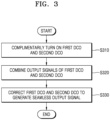
- FIG. 3 is a flowchart illustrating a method of operating a PG-ILCM 200 according to an embodiment.
- the PG-ILCM 200 may complementarily turn on the first DCO 210 and the second DCO 215 (i.e. alternately turn on and off the first DCO 210 and second DCO 215, wherein each of the first DCO 210 and second DSCO 215 are turned on such that when the first DCO 210 is turned on the second DCO 215 is turned off and when the first DCO 210 is turned off the second DCO 215 is turned on).
- the injection pulse width controller 230 in the PG-ILCM 200 may apply a first injection signal S INJA to the first DCO 210 and a second injection signal S INJB to the second DCO 215, respectively.
- the first injection signal S INJA and the second injection signal S INJB may be signals of a same period.
- the first injection signal S INJA and the second injection signal S INJB may have opposite phases to each other. That is, the first injection signal S INJA may be 180 degrees earlier or later than the second injection signal S INJB . Therefore, while the first output signal S OA of the first DCO 210 includes pulses, the second output signal S OB of the second DCO 215 may be "logic low", and while the second output signal S OB of the second DCO 215 includes pulses, the first output signal S OA of the first DCO 210 may be "logic low".
- the PG-ILCM 200 may combine the output signals of the first DCO 210 and the second DCO 215.
- the combining circuit 220 in the PG-ILCM 200 may generate a final output signal S OUT by combining the first output signal S OA of the first DCO 210 and the second output signal S OB of the second DCO 215.
- PVT variations of the first DCO 210 and the second DCO 215 may be different, and accordingly, the first output signal S OA and the second output signal S OB may each include a phase error. Therefore, when the combining circuit 220 simply combines the output signals of the first DCO 210 and the second DCO 215, a final output signal S OUT including discontinuous pulses may be generated.
- the PG-ILCM 200 may correct the first DCO 210 and the second DCO 215 to generate a seamless final output signal.
- the calibration circuit 240 in the PG-ILCM 200 may transmit the first control signal D DA to the first DCO 210, the second control signal D DB to the second DCO 215, and the fourth control signal D IPW to the injection pulse width controller 230.
- the calibration circuit 240 may adjust the first control signal D DA and the second control signal D DB such that the period T DCOA of the first output signal S OA and the period T DCOB of the second output signal S OB are a value obtained by dividing the pulse width PW INJA of the first output signal S OA by an arbitrary natural number N A , and a value obtained by dividing the pulse width PW INJB of the second output signal S OB by an arbitrary natural number N B , respectively.
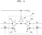
- FIG. 4 illustrates a combining circuit 220 according to an embodiment.
- the combining circuit 220 may include a first inverter 410, a second inverter 420, and a third inverter 430.
- the first inverter 410 may receive the first output signal S OA of the first DCO 210 as an input signal.
- the first inverter 410 may be further connected to the first NMOS transistor 415 so as to be turned on only in a section in which the first output signal S OA includes pulses.
- the first NMOS transistor 415 may be arranged between the first inverter 410 and the ground.
- the first injection signal S INJA may be applied to the gate terminal of the first NMOS transistor 415 and may turn on the first NMOS transistor 415 in the section in which the first output signal S OA includes pulses.
- the first output signal S OA inverted through the first inverter 410 may be inverted again through the third inverter 430 to be output as a portion of the final output signal S OUT .
- the second inverter 420 may receive the second output signal S OB of the second DCO 215 as an input signal.
- the second inverter 420 may be further connected to the second NMOS transistor 425 so as to be turned on only in the section in which the second output signal S OB includes pulses.
- the second NMOS transistor 425 may be arranged between the second inverter 420 and the ground.
- the second injection signal S INJB is applied to the gate terminal of the second NMOS transistor 425 and may turn on the second NMOS transistor 425 in the section in which the second output signal S OB includes pulses.
- the second output signal S OB inverted through the second inverter 420 may be inverted again through the third inverter 430 to be output as a portion of the final output signal S OUT . That is, since the first output signal S OA and the second output signal S OB alternately include pulses, the final output signal S OUT output through the third inverter 430 may be a signal frequency-multiplied by N times.
- FIG. 5 illustrates a calibration circuit 240 according to an embodiment.
- the calibration circuit 240 may include a phase-rotation divider (PR-DIV4) 510, a digitally controlled delay line (DCDL) 520, a bang bang phase detector (BBPD) 530, and a multi control signal generator 540.
- PR-DIV4 phase-rotation divider
- DCDL digitally controlled delay line
- BBPD bang bang phase detector
- multi control signal generator 540 multi control signal generator
- the PR-DIV4 510 may lower the operating frequency of the final output signal S OUT frequency-multiplied by N times to generate a reduced frequency signal S DIV4 .
- the PR-DIV4 510 may lower the operating frequency of the final output signal S OUT by 1/4.
- the DCDL 520 and the BBPD 530 of the next stage may operate at low operating frequencies, which may reduce power consumption.
- the DCDL 520 may delay the reduced frequency signal S DIV4 based on a set offset value to generate a delayed signal S DCDL and output the delayed signal S DCDL to the BBPD 530.
- the BBPD 530 may compare the phase of the delayed signal S DCDL delayed by the DCDL 520 with the phase of the reduced frequency signal S DIV4 .
- the BBPD 530 may provide an output signal PD OUT to the multi control signal generator 540 indicating the result of the comparison between the phase of the delayed signal S DCDL and the phase of the reduced frequency signal S DIV4 .
- the multi control signal generator 540 may provide control signals to the first DCO 210, the second DCO 215, and the injection pulse width controller 230, respectively, on the basis of the output signal PD OUT indicating a result of a phase comparison indicating whether the phase of any one of the delayed signal S DCDL and the reduced frequency signal S DIV4 is earlier.
- the multi control signal generator 540 may provide the first control signal D DA to the first DCO 210.
- the first control signal D DA may be a signal for controlling a frequency of the first output signal S OA .
- the multi control signal generator 540 may generate the first control signal D DA to reduce the period of the first output signal S OA . That is, when the phase of the delayed signal S DCDL is later in phase than the reduced frequency signal S DIV4 , the first control signal D DA having the reduced value may be generated.
- the multi control signal generator 540 may reduce a period of the first output signal S OA by reducing a value of the first control signal D DA .
- the multi control signal generator 540 may provide the second control signal D DB to the second DCO 215.
- the second control signal D DB may be a signal for controlling a frequency of the second output signal S OB .
- the multi control signal generator 540 may generate the second control signal D DB to reduce the period of the second output signal S OB . That is, when the phase of the delayed signal S DCDL is later in phase than the reduced frequency signal S DIV4 , the second control signal D DB having the reduced value may be generated.
- the multi control signal generator 540 may reduce a period of the second output signal S OB by reducing a value of the second control signal D DB .
- the multi control signal generator 540 may provide a third control signal D DCDL to the DCDL 520.
- the third control signal D DCDL may be a signal for controlling how much to delay the reduced frequency signal S DIV4 output by the PR-DIV4 510.
- the multi control signal generator 540 may generate the third control signal D DCDL to reduce the delay time by the DCDL 520.
- the period of the delayed signal S DCDL may be reduced by providing a third control signal D DCDL of a small value to the DCDL 520.
- the period of the delayed signal S DCDL may be reduced until the period of the delayed signal S DCDL becomes twice the period of the first output signal S OA .
- the multi control signal generator 540 may provide the fourth control signal D IPW to the injection pulse width controller 230.
- the fourth control signal D IPW may be a signal for adjusting both the pulse width PW INJA of the first output signal S OA and the pulse width PW INJB of the second output signal S OB .
- the multi control signal generator 540 may generate the fourth control signal D IPW so that a sum of the pulse width PW INJA of the first output signal S OA and the pulse width PW INJB of the second output signal S OB is equal to a reference clock cycle when the output signal PD OUT of the BBPD 530 is one.
- the fourth control signal D IPW may instruct the injection pulse width controller 230 to increase the pulse width PW INJA of the first output signal S OA and decrease the pulse width PW INJB of the second output signal S OB .
- FIG. 6 is a flowchart illustrating a method of operating a calibration circuit 240, according to an embodiment.
- the calibration circuit 240 may adjust a period T DCOA of the first output signal S OA and a period T DCOB of the second output signal S OB according to a phase difference between the reduced frequency signal S DIV4 of the PR-DIV4 510 and the delayed signal S DCDL of the DCDL 520.
- a phase difference may appear between the reduced frequency signal S DIV4 of the PR-DIV4 510 and the delayed signal S DCDL of the DCDL 520.
- This phase difference is because the reduced frequency signal S DIV4 of the PR-DIV4 510 is just injected and generated from the second pulse of the clean second output signal S OB , while the delayed signal S DCDL of the DCDL 520 is generated from the last pulse of the first output signal S OA in which the phase error of the first output signal S OA is accumulated by the period of N A times. Therefore, when the output signal PD OUT of the BBPD 530 is zero at the rising edge of the second pulse of the second output signal S OB , the calibration circuit 240 may generate the first control signal D DA to reduce the period T DCOA of the first output signal S OA .
- the calibration circuit 240 may generate the second control signal D DB to reduce the period T DCOB of the second output signal S OB .
- the calibration circuit 240 may control a delay parameter of the DCDL 520 so that the period of the delayed signal S DCDL of the DCDL 520 is twice the period T DCOA of the first output signal S OA .
- the multi control signal generator 540 of the calibration circuit 240 may generate a third control signal D DCDL that instructs the reduction of the period T DCDL of the delayed signal S DCDL of the DCDL 520.
- the calibration circuit 240 may adjust the pulse width PW INJA of the first output signal S OA and the pulse width PW INJB of the second output signal S OB so that the period T DCDL of the output signal S DCDL of the DCDL 520 is twice the period T DCOB of the second output signal S OB .
- This operation allows the calibration circuit 240 to indirectly compare the period T DCOA of the first output signal S OA with the period T DCOB of the second output signal S OB by means of the period T DCDL of the delayed signal S DCDL of the DCDL 520.
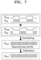
- FIG. 7 illustrates waveforms according to an embodiment.
- the PG-ILCM 200 may complementarily turn on the first DCO 210 and the second DCO 215.
- the first DCO 210 may generate the first output signal S OA including 0.5N pulses by the first injection signal S INJA . Pulses of the first output signal S OA may be generated only during a section in which the first injection signal S INJA is "logic high”.
- the second DCO 215 may generate the second output signal S OB including 0.5N pulses by the second injection signal S INJB .
- the pulses of the second output signal S OB may be generated only during a section in which the second injection signal S INJB is "logic high”.
- pulses of the first output signal S OA and pulses of the second output signal S OB may be alternately generated.
- the PG-ILCM 200 may combine the first output signal S OA and the second output signal S OB through the combining circuit 220. Since the "logic high" sections of the first injection signal S INJA and the second injection signal S INJB do not overlap each other, the final output signal S OUT may include N pulses. However, as illustrated in FIG. 7 , it can be seen that the output signal S OUT includes uneven error pulses such as pulses undergoing transitions to logic low during the rising edges rather than normal pulses, including phase errors. Therefore, when the combining circuit 220 simply combines the first output signal S OA and the second output signal S OB , the output signal S OUT may include discontinuous pulses.
- the calibration circuit 240 controls the period T DCOA of the first output signal S OA and the period T DCOB of the second output signal S OB through phase comparison between pulses with accumulated phase errors and pulses without phase errors, and controls the pulse width PW INJA of the first output signal S OA and the pulse width PW INJB of the second output signal S OB through the period T DCDL of the delayed signal S DCDL of the DCDL 520, to thus generate a final output signal S OUT ' including seamless pulses.
- FIG. 8 is a circuit diagram of an injection pulse width controller 230 according to an embodiment.
- the injection pulse width controller 230 may receive a control signal from the calibration circuit 240.
- the injection pulse width controller 230 may receive a fourth control signal D IPW from the calibration circuit 240, the fourth control signal D IPW instructing the injection pulse width controller 230 to control the pulse width PW INJA of the first output signal S OA and the pulse width PW INJB of the second output signal S OB .
- the fourth control signal D IPW may be a 21-bit control signal.
- the most significant bit MSB of the fourth control signal D IPW may be a bit for indicating whether to increase the pulse width PW INJA of the first output signal S OA or the pulse width PW INJB of the second output signal S OB .
- the most significant bit of the fourth control signal D IPW is "logic low”
- the pulse width PW INJA of the first output signal S OA may be controlled to increase.
- the pulse width PW INJB of the second output signal S OB may be controlled to increase.
- the injection pulse width controller 230 may include a first digital to time converter (DTC A ) 810, a second digital to time converter (DTC B ) 820, and a latch 830.
- DTC A digital to time converter
- DTC B digital to time converter
- the first DTC 810 may convert the remaining 20 bits except for the most significant bit MSB from the fourth control signal D IPW to a time value indicating how long the falling edge of reference clock S REF would be delayed.
- the second DTC 820 may convert the remaining 20 bits except for the most significant bit MSB from the fourth control signal D IPW to a time value indicating how long the rising edge of reference clock S REF would be delayed.
- the latch 830 may output the first injection signal S INJA and the second injection signal S INJB according to the reference clock S REF in which the falling edge is delayed by the time value indicated by the first DTC 810 or the rising edge is delayed by the time value indicated by the second DTC 820.
- FIG. 9A illustrates an example of bidirectional pulse width adjustment according to an embodiment.
- the calibration circuit 240 may provide the injection pulse width controller 230 with a fourth control signal D IPW including the most significant bit of the "logic low" and 20 bits representing the size of 0.2 T DCO .
- the injection pulse width controller 230 may delay the falling edge of the reference clock S REF by 0.2 T DCO based on the most significant bit of the "logic low" in the fourth control signal D IPW , and accordingly, the pulse width PW INJA of the first output signal S OA may be adjusted to 35 T DCO and the pulse width PW INJB of the second output signal S OB may be adjusted to 34 T DCO .
- FIG. 9B illustrates an example of bidirectional pulse width adjustment according to an embodiment.
- the calibration circuit 240 may provide the injection pulse width controller 230 with a fourth control signal D IPW including the most significant bit of the "logic high" and 20 bits representing the size of 0.3 T DCO .
- the injection pulse width controller 230 may delay the falling edge of the reference clock S REF by 0.3 T DCO based on the most significant bit of the "logic high" in the fourth control signal D IPW , and accordingly, the pulse width PW INJA of the first output signal S OA may be adjusted to 31 T DCO and the pulse width PW INJB of the second output signal S OB may be adjusted to 38 T DCO .
- the embodiments described herein provide a PG-ILCM circuit that can multiply frequency up to a higher frequency multiple N than in an ILCM, to achieve high jitter performance at high frequency multiple N.
- the embodiments described herein utilize two digitally controlled oscillators that are alternately switched on and off, and their outputs are combined, where the combined output includes N pulses with a fraction of N coming from each oscillator (e.g. N/2 and N/2). This allows for frequent comparison between turn-on sections of each oscillator, and thus phase shifts of pulses can be monitored and corrected on a continued basis. Thus, even for frequency values where pulses would have smaller injection areas that would otherwise lead to insufficient lock range, the frequency output can be corrected and jitter reduced.
Landscapes
- Physics & Mathematics (AREA)
- Nonlinear Science (AREA)
- Stabilization Of Oscillater, Synchronisation, Frequency Synthesizers (AREA)
Abstract
A frequency multiplier includes a first ring oscillator, a second ring oscillator that is turned on complementarily to the first ring oscillator, a combining circuit that combines a first output signal of the first ring oscillator and a second output signal of the second ring oscillator to generate a final output signal, and a calibration circuit that corrects a discontinuous pulse included in the final output signal based on feedback of the final output signal.
Description
- The present disclosure relates to a frequency multiplier, and more specifically, to a frequency multiplier based on a ring oscillator using power gating injection locking.
- Recently, the need for clock generators with very low jitter and very high output frequencies has emerged as data bandwidth has increased exponentially in various applications such as high-speed interfaces and high bandwidth memory (HBM). Previously, inductor-capacitor (LC) oscillators were mainly used to achieve low jitter, but a ring-voltage controller oscillator (VCO)-based injection locked frequency multiplier with good noise performance even in a small area is attracting attention as an alternative. Ring oscillators have poor free-running noise performance compared to LC oscillators, so it is difficult to achieve low phase noise, but ultra-low noise performance may be achieved based on the ring oscillators by significantly lowering the free-running noise using an injection locked clock multiplier (ILCM) structure with a much wider bandwidth than a phase locked loop (PLL).
- It is an aspect to provide a frequency multiplier that complementarily turns on a ring oscillator using power gating injection locking.
- According to an aspect of one or more embodiments, there is provided a frequency multiplier comprising a first ring oscillator; a second ring oscillator that is turned on complementarily to the first ring oscillator; a combining circuit that combines a first output signal of the first ring oscillator and a second output signal of the second ring oscillator to generate a final output signal; and a calibration circuit that corrects a discontinuous pulse included in the final output signal based on feedback of the final output signal.
- According to another aspect of one or more embodiments, there is provided a frequency multiplier for amplifying a reference clock signal by N times, the frequency multiplier comprising a first ring oscillator that is turned on during a first pulse width of a first injection signal to generate a first output signal; a second ring oscillator that is turned on during a second pulse width of a second injection signal alternating with the first injection signal to generate a second output signal; an injection pulse width controller that controls a ratio of the first pulse width to the second pulse width so that a sum of the first pulse width and the second pulse width is the same as a period of the reference clock signal; a combining circuit that combines the first output signal and the second output signal to generate a final output signal; and a calibration circuit that corrects at least one discontinuous pulse included in the final output signal by controlling at least one of a first frequency of the first injection signal, the first pulse width of the first injection signal, a second frequency of the second injection signal, and the second pulse width of the second injection signal.
- According to yet another aspect of one or more embodiments, there is provided an electronic device comprising a clock generator that generates a reference clock signal; and a frequency multiplier that amplifies a frequency of the reference clock signal by N times. The frequency multiplier comprises a first ring oscillator that is turned on during a first pulse width of a first injection signal, a second ring oscillator that is turned on during a second pulse width of a second injection signal that does not overlap with the first pulse width, a combining circuit that combines a first output signal of the first ring oscillator and a second output signal of the second ring oscillator to generate a final output signal, and a calibration circuit that adjusts at least one of the first pulse width, the second pulse width, a first frequency, and a second frequency to remove a discontinuous pulse included in the final output signal.
- At least some of the above and other features of the invention are set out in the claims.
- Various embodiments will be more clearly understood from the following detailed description taken in conjunction with the accompanying drawings, in which:
-
FIG. 1A is a circuit diagram of a power gating (PG)-ring oscillator (RO) according to an embodiment; -
FIG. 1B illustrates a waveform of a PG-RO according to an embodiment; -
FIG. 2 is a circuit diagram of a power gating (PG)-injection locked clock multiplier (II,CM) according to an embodiment; -
FIG. 3 is a flowchart illustrating a method of operating a PG-ILCM according to an embodiment; -
FIG. 4 illustrates a combining circuit according to an embodiment; -
FIG. 5 illustrates a calibration circuit according to an embodiment; -
FIG. 6 is a flowchart illustrating a method of operating a calibration circuit, according to an embodiment; -
FIG. 7 illustrates waveforms according to an embodiment; -
FIG. 8 is a circuit diagram of an injection pulse width controller according to an embodiment; -
FIG. 9A illustrates an example of bidirectional pulse width adjustment according to an embodiment; and -
FIG. 9B illustrates another example of bidirectional pulse width adjustment according to an embodiment. - In the injection locked clock multiplier (ILCM), a clean reference signal may be injected into the VCO to correct the shaking phase of the VCO and obtain a clean clock signal. As a result, it is easier to achieve better jitter performance in ILCM structures than in PLL structures. However, most of the ILCM structures have low output frequencies because the multiple N (being the number by which the frequency of a signal is to be multiplied) of the ILCM may not be increased as a practical matter. This limitation on the multiple N is because the lock range of the ILCM decreases as the multiple N increases. In order to generate a high output frequency using a low frequency reference clock, N cannot but be inevitably increased. However, in this case, the area of an injection pulse decreases as an output frequency increases, so the amount of injection current that corrects the output phase of an oscillator decreases, and as a result, the lock range decreases. Therefore, there is a need for a method to achieve high jitter performance even at a high frequency multiple N.
- Hereinafter, various embodiments will be described in detail with reference to the accompanying drawings.
-
FIG. 1A is a circuit diagram of a power gating (PG)-ring oscillator (RO) according to an embodiment. A PG-RO 100 may include aring oscillator 110 and aninjection NMOS transistor 120. - Referring to
FIG. 1A , thering oscillator 110 may include M inverters connected in series. Here, M may be a natural odd number. Theinjection NMOS transistor 120 may be arranged between thering oscillator 110 and the ground. The injection signal SINJ of a reference frequency (fREF) may be applied through a gate terminal of theinjection NMOS transistor 120. - Referring to
FIGS. 1A and 1B , the output signal SOUT may include 0.5N pulses during the injection pulse width PWINJ. Here, N may be a frequency multiple. For example, if the frequency multiple is 60 (i.e., generation of a clock with a frequency 60 times higher than a reference clock), the output signal SOUT of an output frequency (fOUT) may contain 30 pulses during the injection pulse width PWINJ. - Referring to
FIG. 1B , the injection signal SINJ may be "logic high" for half of the period, that is, the injection pulse width PWINJ, and may be "logic low" for the other half of the period. Referring toFIG. 1A together withFIG. 1B , since the injection signal SINJ is applied to the gate of theinjection NMOS transistor 120, if the injection signal SINJ is "logic low", theinjection NMOS transistor 120 is turned off, and accordingly, thering oscillator 110 may not operate. Thus, it may be seen that there is no output signal SOUT in the period of the injection signal SINJ that is "logic low" except for the injection pulse width PWINJ. -
FIG. 2 is a circuit diagram of a power gating (PG)-injection locked clock multiplier (ILCM) 200 according to an embodiment. - Referring to
FIG. 2 , the PG-ILCM 200 may include a first digitally controlled oscillator (DCO) 210, asecond DCO 215, a combiningcircuit 220, an injection pulse width controller (IPWC) 230, and acalibration circuit 240. - Each of the
first DCO 210 and thesecond DCO 215 may correspond to an oscillator controlled by a digital signal. For example, each of the first DCO 210 and the second DCO 215 may correspond to the PG-RO 100 illustrated inFIG. 1A . - According to an embodiment, a first output signal SOA of the
first DCO 210 and a second output signal SOB of thesecond DCO 215 may have a phase difference of 180 degrees from each other. For example, while the first output signal SOA includes 0.5N pulses, the second output signal SOB may be "logic low". While the second output signal SOB includes 0.5N pulses, the first output signal SOA may be "logic low". That is, the first injection signal SINJA applied to thefirst DCO 210 and the second injection signal SINJB applied to thesecond DCO 215 may be alternately "logic high". - The combining
circuit 220 may combine the first output signal SOA and the second output signal SOB to generate a final output signal SOUT. As described above, intervals in which the first output signal SOA and the second output signal SOB include 0.5N pulses may be alternately repeated. The combiningcircuit 220 may combine the first output signal SOA and the second output signal SOB to generate a final output signal SOUT including N pulses. - The injection
pulse width controller 230 may generate injection signals applied to thefirst DCO 210 and thesecond DCO 215. For example, the injectionpulse width controller 230 may generate and provide the first injection signal SINJA to thefirst DCO 210 and generate and provide the second injection signal SINJB to thesecond DCO 215. The injectionpulse width controller 230 may adjust the period of the first injection signal SINJA applied to thefirst DCO 210 and the period of the second injection signal SINJB applied to thesecond DCO 215 so that the final output signal SOUT includes N pulses. In this case, a ratio of the period of the first injection signal SINJA to the period of the second injection signal SINJB may be 1:1, but the embodiments are not limited thereto. According to various embodiments, the injectionpulse width controller 230 may adjust the period of the first injection signal SINJA and the period of the second injection signal SINJB to generate a final output signal SOUT including N pulses, respectively, even if a ratio of the period of the first injection signal SINJA to the period of the second injection signal SINJB is not 1:1. - The
calibration circuit 240 may correct a discontinuity included in the final output signal SOUT. For example, each of thefirst DCO 210 and thesecond DCO 215 may have a unique phase error due to process, voltage, and temperature (PVT) variation in each of the first output signal SOA and the second output signal SOB. Accordingly, when the first output signal SOA and the second output signal SOB are simply combined in the combiningcircuit 220, the signals may be discontinuously combined at each point where the first output signal SOA and the second output signal SOB cross each other (e.g., for every injection pulse width PWINJ ofFIG. 1B ). Thecalibration circuit 240 may remove the discontinuity by transmitting control signals to thefirst DCO 210, thesecond DCO 215, and the injectionpulse width controller 230, respectively. For example, thecalibration circuit 240 may correct the frequencies of the first output signal SOA and the second output signal SOB by providing control signals DDA and DDB to thefirst DCO 210 and thesecond DCO 215, respectively. Thecalibration circuit 240 may correct the pulse width of each of the first injection signal SINJA and the second injection signal SINJB by providing a control signal DIPW to the injectionpulse width controller 230. -
FIG. 3 is a flowchart illustrating a method of operating a PG-ILCM 200 according to an embodiment. - Referring to
FIGS. 2 and3 together, in operation S310, the PG-ILCM 200 may complementarily turn on thefirst DCO 210 and the second DCO 215 (i.e. alternately turn on and off thefirst DCO 210 andsecond DCO 215, wherein each of thefirst DCO 210 andsecond DSCO 215 are turned on such that when thefirst DCO 210 is turned on thesecond DCO 215 is turned off and when thefirst DCO 210 is turned off thesecond DCO 215 is turned on). The injectionpulse width controller 230 in the PG-ILCM 200 may apply a first injection signal SINJA to thefirst DCO 210 and a second injection signal SINJB to thesecond DCO 215, respectively. The first injection signal SINJA and the second injection signal SINJB may be signals of a same period. The first injection signal SINJA and the second injection signal SINJB may have opposite phases to each other. That is, the first injection signal SINJA may be 180 degrees earlier or later than the second injection signal SINJB. Therefore, while the first output signal SOA of thefirst DCO 210 includes pulses, the second output signal SOB of thesecond DCO 215 may be "logic low", and while the second output signal SOB of thesecond DCO 215 includes pulses, the first output signal SOA of thefirst DCO 210 may be "logic low". - In operation S320, the PG-
ILCM 200 may combine the output signals of thefirst DCO 210 and thesecond DCO 215. The combiningcircuit 220 in the PG-ILCM 200 may generate a final output signal SOUT by combining the first output signal SOA of thefirst DCO 210 and the second output signal SOB of thesecond DCO 215. However, PVT variations of thefirst DCO 210 and thesecond DCO 215 may be different, and accordingly, the first output signal SOA and the second output signal SOB may each include a phase error. Therefore, when the combiningcircuit 220 simply combines the output signals of thefirst DCO 210 and thesecond DCO 215, a final output signal SOUT including discontinuous pulses may be generated. - In operation S330, the PG-
ILCM 200 may correct thefirst DCO 210 and thesecond DCO 215 to generate a seamless final output signal. For example, thecalibration circuit 240 in the PG-ILCM 200 may transmit the first control signal DDA to thefirst DCO 210, the second control signal DDB to thesecond DCO 215, and the fourth control signal DIPW to the injectionpulse width controller 230. Thecalibration circuit 240 may adjust the first control signal DDA and the second control signal DDB such that the period TDCOA of the first output signal SOA and the period TDCOB of the second output signal SOB are a value obtained by dividing the pulse width PWINJA of the first output signal SOA by an arbitrary natural number NA, and a value obtained by dividing the pulse width PWINJB of the second output signal SOB by an arbitrary natural number NB, respectively. -
FIG. 4 illustrates a combiningcircuit 220 according to an embodiment. - Referring to
FIG. 4 , the combiningcircuit 220 may include a first inverter 410, asecond inverter 420, and athird inverter 430. - The first inverter 410 may receive the first output signal SOA of the
first DCO 210 as an input signal. The first inverter 410 may be further connected to thefirst NMOS transistor 415 so as to be turned on only in a section in which the first output signal SOA includes pulses. For example, thefirst NMOS transistor 415 may be arranged between the first inverter 410 and the ground. The first injection signal SINJA may be applied to the gate terminal of thefirst NMOS transistor 415 and may turn on thefirst NMOS transistor 415 in the section in which the first output signal SOA includes pulses. The first output signal SOA inverted through the first inverter 410 may be inverted again through thethird inverter 430 to be output as a portion of the final output signal SOUT. - The
second inverter 420 may receive the second output signal SOB of thesecond DCO 215 as an input signal. Thesecond inverter 420 may be further connected to thesecond NMOS transistor 425 so as to be turned on only in the section in which the second output signal SOB includes pulses. For example, thesecond NMOS transistor 425 may be arranged between thesecond inverter 420 and the ground. The second injection signal SINJB is applied to the gate terminal of thesecond NMOS transistor 425 and may turn on thesecond NMOS transistor 425 in the section in which the second output signal SOB includes pulses. The second output signal SOB inverted through thesecond inverter 420 may be inverted again through thethird inverter 430 to be output as a portion of the final output signal SOUT. That is, since the first output signal SOA and the second output signal SOB alternately include pulses, the final output signal SOUT output through thethird inverter 430 may be a signal frequency-multiplied by N times. -
FIG. 5 illustrates acalibration circuit 240 according to an embodiment. - Referring to
FIG. 5 , thecalibration circuit 240 may include a phase-rotation divider (PR-DIV4) 510, a digitally controlled delay line (DCDL) 520, a bang bang phase detector (BBPD) 530, and a multicontrol signal generator 540. - The PR-
DIV4 510 may lower the operating frequency of the final output signal SOUT frequency-multiplied by N times to generate a reduced frequency signal SDIV4. For example, in an embodiment, the PR-DIV4 510 may lower the operating frequency of the final output signal SOUT by 1/4. By lowering the operating frequency of the final output signal SOUT through the PR-DIV4 510, theDCDL 520 and theBBPD 530 of the next stage may operate at low operating frequencies, which may reduce power consumption. - The
DCDL 520 may delay the reduced frequency signal SDIV4 based on a set offset value to generate a delayed signal SDCDL and output the delayed signal SDCDL to theBBPD 530. TheBBPD 530 may compare the phase of the delayed signal SDCDL delayed by theDCDL 520 with the phase of the reduced frequency signal SDIV4 . TheBBPD 530 may provide an output signal PDOUT to the multicontrol signal generator 540 indicating the result of the comparison between the phase of the delayed signal SDCDL and the phase of the reduced frequency signal SDIV4. - The multi
control signal generator 540 may provide control signals to thefirst DCO 210, thesecond DCO 215, and the injectionpulse width controller 230, respectively, on the basis of the output signal PDOUT indicating a result of a phase comparison indicating whether the phase of any one of the delayed signal SDCDL and the reduced frequency signal SDIV4 is earlier. - According to an embodiment, the multi
control signal generator 540 may provide the first control signal DDA to thefirst DCO 210. The first control signal DDA may be a signal for controlling a frequency of the first output signal SOA. For example, when the output signal PDOUT of theBBPD 530 is zero at the rising edge of the fourth pulse of the second output signal SOB, the multicontrol signal generator 540 may generate the first control signal DDA to reduce the period of the first output signal SOA. That is, when the phase of the delayed signal SDCDL is later in phase than the reduced frequency signal SDIV4, the first control signal DDA having the reduced value may be generated. The multicontrol signal generator 540 may reduce a period of the first output signal SOA by reducing a value of the first control signal DDA. - According to an embodiment, the multi
control signal generator 540 may provide the second control signal DDB to thesecond DCO 215. The second control signal DDB may be a signal for controlling a frequency of the second output signal SOB. For example, when the output signal PDOUT of theBBPD 530 is zero at the rising edge of the fourth pulse of the first output signal SOA, the multicontrol signal generator 540 may generate the second control signal DDB to reduce the period of the second output signal SOB. That is, when the phase of the delayed signal SDCDL is later in phase than the reduced frequency signal SDIV4, the second control signal DDB having the reduced value may be generated. The multicontrol signal generator 540 may reduce a period of the second output signal SOB by reducing a value of the second control signal DDB. - According to an embodiment, the multi
control signal generator 540 may provide a third control signal DDCDL to theDCDL 520. The third control signal DDCDL may be a signal for controlling how much to delay the reduced frequency signal SDIV4 output by the PR-DIV4 510. For example, when the output signal PDOUT of theBBPD 530 is zero at the rising edge of the last pulse of the first output signal SOA, the multicontrol signal generator 540 may generate the third control signal DDCDL to reduce the delay time by theDCDL 520. The period of the delayed signal SDCDL may be reduced by providing a third control signal DDCDL of a small value to theDCDL 520. The period of the delayed signal SDCDL may be reduced until the period of the delayed signal SDCDL becomes twice the period of the first output signal SOA. - According to an embodiment, the multi
control signal generator 540 may provide the fourth control signal DIPW to the injectionpulse width controller 230. The fourth control signal DIPW may be a signal for adjusting both the pulse width PWINJA of the first output signal SOA and the pulse width PWINJB of the second output signal SOB. For example, at the rising edge of the last pulse of the second output signal SOB, the multicontrol signal generator 540 may generate the fourth control signal DIPW so that a sum of the pulse width PWINJA of the first output signal SOA and the pulse width PWINJB of the second output signal SOB is equal to a reference clock cycle when the output signal PDOUT of theBBPD 530 is one. When the output signal PDOUT of theBBPD 530 is one, the fourth control signal DIPW may instruct the injectionpulse width controller 230 to increase the pulse width PWINJA of the first output signal SOA and decrease the pulse width PWINJB of the second output signal SOB. -
FIG. 6 is a flowchart illustrating a method of operating acalibration circuit 240, according to an embodiment. - Referring to
FIG. 6 , in operation S610, thecalibration circuit 240 may adjust a period TDCOA of the first output signal SOA and a period TDCOB of the second output signal SOB according to a phase difference between the reduced frequency signal SDIV4 of the PR-DIV4 510 and the delayed signal SDCDL of theDCDL 520. For example, when the period TDCOA of the first output signal SOA does not satisfy a value obtained by dividing the pulse width PWINJA of the first output signal SOA by any natural number NA, a phase difference may appear between the reduced frequency signal SDIV4 of the PR-DIV4 510 and the delayed signal SDCDL of theDCDL 520. This phase difference is because the reduced frequency signal SDIV4 of the PR-DIV4 510 is just injected and generated from the second pulse of the clean second output signal SOB, while the delayed signal SDCDL of theDCDL 520 is generated from the last pulse of the first output signal SOA in which the phase error of the first output signal SOA is accumulated by the period of NA times. Therefore, when the output signal PDOUT of theBBPD 530 is zero at the rising edge of the second pulse of the second output signal SOB, thecalibration circuit 240 may generate the first control signal DDA to reduce the period TDCOA of the first output signal SOA. When the output signal PDOUT of theBBPD 530 is zero at the rising edge of the second pulse of the first output signal SOA, thecalibration circuit 240 may generate the second control signal DDB to reduce the period TDCOB of the second output signal SOB. - In operation S620, the
calibration circuit 240 may control a delay parameter of theDCDL 520 so that the period of the delayed signal SDCDL of theDCDL 520 is twice the period TDCOA of the first output signal SOA. For example, when the output signal PDOUT of theBBPD 530 is zero at the rising edge of the last pulse of the first output signal SOA, the multicontrol signal generator 540 of thecalibration circuit 240 may generate a third control signal DDCDL that instructs the reduction of the period TDCDL of the delayed signal SDCDL of theDCDL 520. - In operation S630, the
calibration circuit 240 may adjust the pulse width PWINJA of the first output signal SOA and the pulse width PWINJB of the second output signal SOB so that the period TDCDL of the output signal SDCDL of theDCDL 520 is twice the period TDCOB of the second output signal SOB. This operation allows thecalibration circuit 240 to indirectly compare the period TDCOA of the first output signal SOA with the period TDCOB of the second output signal SOB by means of the period TDCDL of the delayed signal SDCDL of theDCDL 520. -
FIG. 7 illustrates waveforms according to an embodiment. - Referring to
FIG. 7 , the PG-ILCM 200 may complementarily turn on thefirst DCO 210 and thesecond DCO 215. For example, thefirst DCO 210 may generate the first output signal SOA including 0.5N pulses by the first injection signal SINJA. Pulses of the first output signal SOA may be generated only during a section in which the first injection signal SINJA is "logic high". Thesecond DCO 215 may generate the second output signal SOB including 0.5N pulses by the second injection signal SINJB. The pulses of the second output signal SOB may be generated only during a section in which the second injection signal SINJB is "logic high". As shown inFIG. 7 , since the first injection signal SINJA and the second injection signal SINJB have phase difference of 180 degrees, pulses of the first output signal SOA and pulses of the second output signal SOB may be alternately generated. - The PG-
ILCM 200 may combine the first output signal SOA and the second output signal SOB through the combiningcircuit 220. Since the "logic high" sections of the first injection signal SINJA and the second injection signal SINJB do not overlap each other, the final output signal SOUT may include N pulses. However, as illustrated inFIG. 7 , it can be seen that the output signal SOUT includes uneven error pulses such as pulses undergoing transitions to logic low during the rising edges rather than normal pulses, including phase errors. Therefore, when the combiningcircuit 220 simply combines the first output signal SOA and the second output signal SOB, the output signal SOUT may include discontinuous pulses. - Therefore, the
calibration circuit 240 controls the period TDCOA of the first output signal SOA and the period TDCOB of the second output signal SOB through phase comparison between pulses with accumulated phase errors and pulses without phase errors, and controls the pulse width PWINJA of the first output signal SOA and the pulse width PWINJB of the second output signal SOB through the period TDCDL of the delayed signal SDCDL of theDCDL 520, to thus generate a final output signal SOUT' including seamless pulses. -
FIG. 8 is a circuit diagram of an injectionpulse width controller 230 according to an embodiment. - Referring to
FIG. 8 , the injectionpulse width controller 230 may receive a control signal from thecalibration circuit 240. For example, the injectionpulse width controller 230 may receive a fourth control signal DIPW from thecalibration circuit 240, the fourth control signal DIPW instructing the injectionpulse width controller 230 to control the pulse width PWINJA of the first output signal SOA and the pulse width PWINJB of the second output signal SOB. In some embodiments, the fourth control signal DIPW may be a 21-bit control signal. - According to an embodiment, the most significant bit MSB of the fourth control signal DIPW may be a bit for indicating whether to increase the pulse width PWINJA of the first output signal SOA or the pulse width PWINJB of the second output signal SOB. For example, when the most significant bit of the fourth control signal DIPW is "logic low", the pulse width PWINJA of the first output signal SOA may be controlled to increase. When the most significant bit of the fourth control signal DIPW is "logic high", the pulse width PWINJB of the second output signal SOB may be controlled to increase.
- The injection
pulse width controller 230 may include a first digital to time converter (DTCA) 810, a second digital to time converter (DTCB) 820, and alatch 830. When thefirst DTC 810 adjusts the pulse width PWINJA of the first output signal SOA, thefirst DTC 810 may convert the remaining 20 bits except for the most significant bit MSB from the fourth control signal DIPW to a time value indicating how long the falling edge of reference clock SREF would be delayed. When thesecond DTC 820 adjusts the pulse width PWINJB of the second output signal SOB, thesecond DTC 820 may convert the remaining 20 bits except for the most significant bit MSB from the fourth control signal DIPW to a time value indicating how long the rising edge of reference clock SREF would be delayed. Thelatch 830 may output the first injection signal SINJA and the second injection signal SINJB according to the reference clock SREF in which the falling edge is delayed by the time value indicated by thefirst DTC 810 or the rising edge is delayed by the time value indicated by thesecond DTC 820. -
FIG. 9A illustrates an example of bidirectional pulse width adjustment according to an embodiment. - Referring to
FIG. 9A , according to an embodiment, the duty cycle of the final output signal SOUT may be 50.9 %. That is, when the frequency multiple N=69, the pulse width PWINJA of the first output signal SOA may be 34.8 TDCO, and the pulse width PWINJB of the second output signal SOB may be 34.2 TDCO. In order to make the pulse width PWINJA of the first output signal SOA and the pulse width PWINJB of the second output signal SOB at the same time as an integer multiple of the period TDCO of the reference clock SREF, the smallest adjustment may be implemented by reducing the pulse width PWINJB of the second output signal SOB by 0.2 TDCO, and may be implemented by increasing the pulse width PWINJA of the first output signal SOA by 0.2 TDCO. Therefore, thecalibration circuit 240 may provide the injectionpulse width controller 230 with a fourth control signal DIPW including the most significant bit of the "logic low" and 20 bits representing the size of 0.2 TDCO. The injectionpulse width controller 230 may delay the falling edge of the reference clock SREF by 0.2 TDCO based on the most significant bit of the "logic low" in the fourth control signal DIPW, and accordingly, the pulse width PWINJA of the first output signal SOA may be adjusted to 35 TDCO and the pulse width PWINJB of the second output signal SOB may be adjusted to 34 TDCO. -
FIG. 9B illustrates an example of bidirectional pulse width adjustment according to an embodiment. - Referring to
FIG. 9B , according to an embodiment, the duty cycle of the final output signal SOUT may be 45.3 %. That is, when the frequency multiple N=69, the pulse width PWINJA of the first output signal SOA may be 31.3 TDCO, and the pulse width PWINJB of the second output signal SOB may be 37.7 TDCO. In order to make the pulse width PWINJA of the first output signal SOA and the pulse width PWINJB of the second output signal SOB at the same time as an integer multiple of the period TDCO of the reference clock SREF, the smallest adjustment may be implemented by increasing the pulse width PWINJB of the second output signal SOB by 0.3 TDCO, and may be implemented by reducing the pulse width PWINJA of the first output signal SOA by 0.3 TDCO. Therefore, thecalibration circuit 240 may provide the injectionpulse width controller 230 with a fourth control signal DIPW including the most significant bit of the "logic high" and 20 bits representing the size of 0.3 TDCO. The injectionpulse width controller 230 may delay the falling edge of the reference clock SREF by 0.3 TDCO based on the most significant bit of the "logic high" in the fourth control signal DIPW, and accordingly, the pulse width PWINJA of the first output signal SOA may be adjusted to 31 TDCO and the pulse width PWINJB of the second output signal SOB may be adjusted to 38 TDCO. - The embodiments described herein provide a PG-ILCM circuit that can multiply frequency up to a higher frequency multiple N than in an ILCM, to achieve high jitter performance at high frequency multiple N. The embodiments described herein utilize two digitally controlled oscillators that are alternately switched on and off, and their outputs are combined, where the combined output includes N pulses with a fraction of N coming from each oscillator (e.g. N/2 and N/2). This allows for frequent comparison between turn-on sections of each oscillator, and thus phase shifts of pulses can be monitored and corrected on a continued basis. Thus, even for frequency values where pulses would have smaller injection areas that would otherwise lead to insufficient lock range, the frequency output can be corrected and jitter reduced.
- While various embodiments have been particularly shown and described with reference to the drawings, it will be understood that various changes in form and details may be made therein without departing from the scope of the following claims.
- Further Embodiments are set out in the following clauses:
- Clause 1. A frequency multiplier comprising:
- a first ring oscillator;
- a second ring oscillator that is turned on complementarily to the first ring oscillator;
- a combining circuit that combines a first output signal of the first ring oscillator and a second output signal of the second ring oscillator to generate a final output signal; and
- a calibration circuit that corrects a discontinuous pulse included in the final output signal based on feedback of the final output signal.
-
Clause 2. The frequency multiplier of clause 1, further comprising an injection pulse width controller that injects a first injection signal into the first ring oscillator and injects a second injection signal into the second ring oscillator,
wherein the first injection signal and the second injection signal are alternately changed to logic high. - Clause 3. The frequency multiplier of
clause 2, wherein the combining circuit comprises:- a first inverter that is turned on according to the first injection signal and inverts the first output signal of the first ring oscillator;
- a second inverter that is turned on according to the second injection signal and inverts the second output signal of the second ring oscillator; and
- a third inverter connected to an output end of the first inverter and the second inverter, the third inverter inverting the inverted first output signal to output the first output signal during a logic high of the first injection signal, and generating the final output signal by inverting the inverted second output signal to output the second output signal during a logic high of the second injection signal.
- Clause 4. The frequency multiplier of any one of clauses 2 - 4, wherein the calibration circuit comprises a phase-rotation divider, a digital control delay line, a phase detector, and a multi control signal generator.
- Clause 5. The frequency multiplier of clause 4, wherein the phase-rotation divider reduces an operating frequency of the final output signal by 1/4 to generate a reduced frequency signal, and outputs the reduced frequency signal.
- Clause 6. The frequency multiplier of clause 5, wherein the digital control delay line delays, by a predefined value, the reduced frequency signal to generate a delayed signal, and outputs the delayed signal.
- Clause 7. The frequency multiplier of clause 6, wherein the phase detector detects a phase difference between the reduced frequency signal and the delayed signal.
- Clause 8. The frequency multiplier of clause 7, wherein the multi control signal generator generates:
- a first control signal provided to the first ring oscillator to adjust a frequency of the first output signal;
- a second control signal provided to the second ring oscillator to adjust a frequency of the second output signal;
- a third control signal provided to the digital control delay line to adjust the predefined value; and
- a fourth control signal provided to the injection pulse width controller to adjust a first pulse width of the first injection signal and a second pulse width of the second injection signal.
- Clause 9. An electronic device comprising:
- a clock generator that generates a reference clock signal; and
- a frequency multiplier that amplifies a frequency of the reference clock signal by N times, wherein the frequency multiplier comprises:
- a first ring oscillator that is turned on during a first pulse width of a first injection signal,
- a second ring oscillator that is turned on during a second pulse width of a second injection signal that does not overlap with the first pulse width,
- a combining circuit that combines a first output signal of the first ring oscillator and a second output signal of the second ring oscillator to generate a final output signal, and
- a calibration circuit that adjusts at least one of the first pulse width, the second pulse width, a first frequency, and a second frequency to remove a discontinuous pulse included in the final output signal.
- Clause 10. The electronic device of clause 9, wherein a sum of the first pulse width and the second pulse width is the same as a period of the reference clock signal.
- Clause 11. The electronic device of clause 9 or clause 10, wherein the calibration circuit comprises:
a phase-rotation divider, a digital control delay line, a phase detector, and a multi control signal generator. - Clause 12. The electronic device of clause 11, wherein:
- the phase-rotation divider reduces an operating frequency of the final output signal by 1/4 to generate a reduced frequency signal, and outputs the reduced frequency signal,
- the digital control delay line delays, by a predefined value, the reduced frequency signal to generate a delayed signal, and outputs the delayed signal,
- the phase detector detects a phase difference between the reduced frequency signal and the delayed signal.
- Clause 13. The electronic device of clause 12, wherein the multi control signal generator generates a first control signal provided to the first ring oscillator to adjust a frequency of the first output signal, a second control signal provided to the second ring oscillator to adjust a frequency of the second output signal, a third control signal provided to the digital control delay line to adjust the predefined value, and a fourth control signal to adjust the first pulse width of the first injection signal and the second pulse width of the second injection signal.
- Clause 14. The electronic device of clause 13, wherein the calibration circuit is configured to:
adjust a first period of a plurality of pulses included in the first output signal to be equal to a value obtained by dividing the first pulse width of the first injection signal by a first value. - Clause 15. The electronic device of clause 14, wherein the calibration circuit is configured to:
- adjust a second period of a plurality of pulses included in the second output signal to be equal to a value obtained by dividing the second pulse width of the second injection signal by a second value, and
- adjust a period of the delayed signal to be equal to twice the first period,
- wherein a sum of the first value and the second value is the same as a value of N.
Claims (12)
- A frequency multiplier comprising:a first ring oscillator;a second ring oscillator configured to be turned on complementarily to the first ring oscillator;a combining circuit configured to combine a first output signal of the first ring oscillator and a second output signal of the second ring oscillator to generate a final output signal; anda calibration circuit configured to correct a discontinuous pulse included in the final output signal based on feedback of the final output signal.
- The frequency multiplier of claim 1, further comprising an injection pulse width controller that is configured to inject a first injection signal into the first ring oscillator and to inject a second injection signal into the second ring oscillator,
wherein the first injection signal and the second injection signal are alternately changed to logic high. - The frequency multiplier of claim 2, wherein the combining circuit comprises:a first inverter configured to be turned on according to the first injection signal and to invert the first output signal of the first ring oscillator;a second inverter configured to be turned on according to the second injection signal and to invert the second output signal of the second ring oscillator; anda third inverter connected to an output end of the first inverter and the second inverter, the third inverter configured to invert the inverted first output signal to output the first output signal during a logic high of the first injection signal, and configured to generate the final output signal by inverting the inverted second output signal to output the second output signal during a logic high of the second injection signal.
- The frequency multiplier of any one of claims 2 - 4, wherein the calibration circuit comprises a phase-rotation divider, a digital control delay line, a phase detector, and a multi control signal generator.
- The frequency multiplier of claim 4, wherein the phase-rotation divider is configured to reduce an operating frequency of the final output signal by 1/4 to generate a reduced frequency signal, the phase-rotation divider further configured to output the reduced frequency signal.
- The frequency multiplier of claim 5, wherein the digital control delay line is configured to delay, by a predefined value, the reduced frequency signal to generate a delayed signal, and to output the delayed signal.
- The frequency multiplier of claim 6, wherein the phase detector is configured to detect a phase difference between the reduced frequency signal and the delayed signal.
- The frequency multiplier of claim 7, wherein the multi control signal generator is configured to generate:a first control signal provided to the first ring oscillator to adjust a frequency of the first output signal;a second control signal provided to the second ring oscillator to adjust a frequency of the second output signal;a third control signal provided to the digital control delay line to adjust the predefined value; anda fourth control signal provided to the injection pulse width controller to adjust a first pulse width of the first injection signal and a second pulse width of the second injection signal.
- The electronic device of claim 8, wherein the calibration circuit is further configured to:
adjust a first period of a plurality of pulses included in the first output signal to be equal to a value obtained by dividing the first pulse width of the first injection signal by a first value. - The electronic device of claim 9, wherein the calibration circuit is configured to:adjust a second period of a plurality of pulses included in the second output signal to be equal to a value obtained by dividing the second pulse width of the second injection signal by a second value, andadjust a period of the delayed signal to be equal to twice the first period,wherein a sum of the first value and the second value is the same as a value of N.
- An electronic device comprising:a clock generator that generates a reference clock signal; anda frequency multiplier according to any preceding claim,:wherein the first ring oscillator is turned on during a first pulse width of a first injection signal,wherein the second ring oscillator is turned on during a second pulse width of a second injection signal that does not overlap with the first pulse width, andwherein the calibration circuit being configured to remove a discontinuous pulse included in the final output signal comprises the calibration circuit being configured to adjust at least one of the first pulse width, the second pulse width, a first frequency, and a second frequency.
- The electronic device of claim 11, wherein a sum of the first pulse width and the second pulse width is the same as a period of the reference clock signal.
Applications Claiming Priority (2)
| Application Number | Priority Date | Filing Date | Title |
|---|---|---|---|
| KR20230014456 | 2023-02-02 | ||
| KR1020230061262A KR20240121643A (en) | 2023-02-02 | 2023-05-11 | Frequency multiplier based on ring oscillator using power gating injection locking |
Publications (1)
| Publication Number | Publication Date |
|---|---|
| EP4412088A1 true EP4412088A1 (en) | 2024-08-07 |
Family
ID=89843611
Family Applications (1)
| Application Number | Title | Priority Date | Filing Date |
|---|---|---|---|
| EP24155512.7A Withdrawn EP4412088A1 (en) | 2023-02-02 | 2024-02-02 | Frequency multiplier based on ring oscillator using power gating injection locking |
Country Status (2)
| Country | Link |
|---|---|
| US (1) | US12574019B2 (en) |
| EP (1) | EP4412088A1 (en) |
Citations (1)
| Publication number | Priority date | Publication date | Assignee | Title |
|---|---|---|---|---|
| US6104326A (en) * | 1997-10-14 | 2000-08-15 | Electronics And Telecommunications Research Institute | Bit synchronization apparatus for recovering high speed NRZ data |
Family Cites Families (5)
| Publication number | Priority date | Publication date | Assignee | Title |
|---|---|---|---|---|
| US8941420B2 (en) | 2011-07-01 | 2015-01-27 | Rambus Inc. | Low-latency, frequency-agile clock multiplier |
| US10020931B2 (en) | 2013-03-07 | 2018-07-10 | Intel Corporation | Apparatus for dynamically adapting a clock generator with respect to changes in power supply |
| JP7103894B2 (en) | 2018-08-30 | 2022-07-20 | ラピスセミコンダクタ株式会社 | Phase-locked loop |
| FR3086132B1 (en) | 2018-09-19 | 2020-10-09 | Commissariat Energie Atomique | HIGH MULTIPLICATION RANK FREQUENCY SYNTHESIS DEVICE |
| US10998910B1 (en) * | 2020-02-11 | 2021-05-04 | Marvell Asia Pte, Ltd. | Method and apparatus for controlling clock cycle time |
-
2024
- 2024-02-02 EP EP24155512.7A patent/EP4412088A1/en not_active Withdrawn
- 2024-02-02 US US18/431,449 patent/US12574019B2/en active Active
Patent Citations (1)
| Publication number | Priority date | Publication date | Assignee | Title |
|---|---|---|---|---|
| US6104326A (en) * | 1997-10-14 | 2000-08-15 | Electronics And Telecommunications Research Institute | Bit synchronization apparatus for recovering high speed NRZ data |
Non-Patent Citations (3)
| Title |
|---|
| LEE YONGSUN ET AL: "A Low Phase Noise Injection-Locked Programmable Reference Clock Multiplier With a Two-Phase PVT-Calibrator for $\Delta\Sigma$ PLLs", IEEE TRANSACTIONS ON CIRCUITS AND SYSTEMS I: REGULAR PAPERS, IEEE, US, vol. 62, no. 3, 1 March 2015 (2015-03-01), pages 635 - 644, XP011573892, ISSN: 1549-8328, [retrieved on 20150223], DOI: 10.1109/TCSI.2014.2370191 * |
| PARK SUNEUI ET AL: "A 97fsrms-Jitter and 68-Multiplication Factor, 8.16GHz Ring-Oscillator Injection-Locked Clock Multiplier with Power-Gating Injection-Locking and Background Multi-Functional Digital Calibrator", 2022 IEEE INTERNATIONAL SOLID- STATE CIRCUITS CONFERENCE (ISSCC), IEEE, vol. 65, 20 February 2022 (2022-02-20), pages 1 - 3, XP034102932, DOI: 10.1109/ISSCC42614.2022.9731713 * |
| PARK SUNEUI ET AL: "A Sub-100 fs-Jitter 8.16-GHz Ring-Oscillator-Based Power-Gating Injection-Locked Clock Multiplier With the Multiplication Factor of 68", IEEE JOURNAL OF SOLID-STATE CIRCUITS, vol. 58, no. 1, 1 January 2023 (2023-01-01), USA, pages 78 - 89, XP093179419, ISSN: 0018-9200, Retrieved from the Internet <URL:https://ieeexplore.ieee.org/stampPDF/getPDF.jsp?tp=&arnumber=9914018&ref=aHR0cHM6Ly9pZWVleHBsb3JlLmllZWUub3JnL2RvY3VtZW50Lzk5MTQwMTg=> [retrieved on 20240626], DOI: 10.1109/JSSC.2022.3210212 * |
Also Published As
| Publication number | Publication date |
|---|---|
| US12574019B2 (en) | 2026-03-10 |
| US20240267037A1 (en) | 2024-08-08 |
Similar Documents
| Publication | Publication Date | Title |
|---|---|---|
| US7605666B2 (en) | High frequency digital oscillator-on-demand with synchronization | |
| US8085101B2 (en) | Spread spectrum clock generation device | |
| JP4660076B2 (en) | Clock generation circuit | |
| US7772900B2 (en) | Phase-locked loop circuits and methods implementing pulsewidth modulation for fine tuning control of digitally controlled oscillators | |
| CN113364457B (en) | A quadruple frequency circuit | |
| US20100176852A1 (en) | Spread spectrum clock generator using arrival locked loop technology | |
| US11342923B1 (en) | Circuit and method for random edge injection locking | |
| US20050146366A1 (en) | High-resolution digital pulse width modulator and method for generating a high-resolution pulse width modulated signal | |
| KR20080038777A (en) | Clock data recovery device. | |
| US6946887B2 (en) | Phase frequency detector with programmable minimum pulse width | |
| US20120161827A1 (en) | Central lc pll with injection locked ring pll or dell per lane | |
| Park et al. | A 97fs rms-Jitter and 68-Multiplication Factor, 8.16 GHz Ring-Oscillator Injection-Locked Clock Multiplier with Power-Gating Injection-Locking and Background Multi-Functional Digital Calibrator | |
| US7372340B2 (en) | Precision frequency and phase synthesis with fewer voltage-controlled oscillator stages | |
| US12574019B2 (en) | Frequency multiplier based on ring oscillator using power gating injection locking | |
| US11509296B2 (en) | Clock generator for frequency multiplication | |
| KR100531457B1 (en) | Delay Locked Loop For Generating Multi-Phase Clocks Without Voltage-Controlled Oscillator | |
| US7113014B1 (en) | Pulse width modulator | |
| US10236866B2 (en) | Pulse width modulation signal frequency generation | |
| US20090167442A1 (en) | Low noise wide range voltage-controlled oscillator with transistor feedback | |
| US7498887B1 (en) | High frequency digital oscillator-on-demand with synchronization | |
| KR20240121643A (en) | Frequency multiplier based on ring oscillator using power gating injection locking | |
| CN118432609A (en) | Frequency Multiplier Based on Ring Oscillator Using Power-Gated Injection Locking | |
| JP2010074562A (en) | Pll circuit | |
| US10560053B2 (en) | Digital fractional frequency divider | |
| JP4242712B2 (en) | Clock generation circuit |
Legal Events
| Date | Code | Title | Description |
|---|---|---|---|
| PUAI | Public reference made under article 153(3) epc to a published international application that has entered the european phase |
Free format text: ORIGINAL CODE: 0009012 |
|
| STAA | Information on the status of an ep patent application or granted ep patent |
Free format text: STATUS: THE APPLICATION HAS BEEN PUBLISHED |
|
| AK | Designated contracting states |
Kind code of ref document: A1 Designated state(s): AL AT BE BG CH CY CZ DE DK EE ES FI FR GB GR HR HU IE IS IT LI LT LU LV MC ME MK MT NL NO PL PT RO RS SE SI SK SM TR |
|
| STAA | Information on the status of an ep patent application or granted ep patent |
Free format text: STATUS: THE APPLICATION IS DEEMED TO BE WITHDRAWN |
|
| 18D | Application deemed to be withdrawn |
Effective date: 20250208 |