EP4412066A1 - Multi-phase ac-dc converter - Google Patents
Multi-phase ac-dc converter Download PDFInfo
- Publication number
- EP4412066A1 EP4412066A1 EP24152938.7A EP24152938A EP4412066A1 EP 4412066 A1 EP4412066 A1 EP 4412066A1 EP 24152938 A EP24152938 A EP 24152938A EP 4412066 A1 EP4412066 A1 EP 4412066A1
- Authority
- EP
- European Patent Office
- Prior art keywords
- bridge
- converter
- active
- switches
- terminal
- Prior art date
- Legal status (The legal status is an assumption and is not a legal conclusion. Google has not performed a legal analysis and makes no representation as to the accuracy of the status listed.)
- Pending
Links
- 230000010363 phase shift Effects 0.000 claims abstract description 29
- 239000003990 capacitor Substances 0.000 claims description 102
- 230000007935 neutral effect Effects 0.000 claims description 37
- 230000000903 blocking effect Effects 0.000 claims description 13
- 230000000295 complement effect Effects 0.000 description 13
- 230000002457 bidirectional effect Effects 0.000 description 4
- 238000006243 chemical reaction Methods 0.000 description 4
- 238000010586 diagram Methods 0.000 description 3
- 230000005669 field effect Effects 0.000 description 2
- 230000001105 regulatory effect Effects 0.000 description 2
- 239000004065 semiconductor Substances 0.000 description 2
- 238000011217 control strategy Methods 0.000 description 1
- 230000001419 dependent effect Effects 0.000 description 1
- 238000005516 engineering process Methods 0.000 description 1
- 238000002955 isolation Methods 0.000 description 1
Images








Classifications
-
- H—ELECTRICITY
- H02—GENERATION; CONVERSION OR DISTRIBUTION OF ELECTRIC POWER
- H02M—APPARATUS FOR CONVERSION BETWEEN AC AND AC, BETWEEN AC AND DC, OR BETWEEN DC AND DC, AND FOR USE WITH MAINS OR SIMILAR POWER SUPPLY SYSTEMS; CONVERSION OF DC OR AC INPUT POWER INTO SURGE OUTPUT POWER; CONTROL OR REGULATION THEREOF
- H02M1/00—Details of apparatus for conversion
- H02M1/0095—Hybrid converter topologies, e.g. NPC mixed with flying capacitor, thyristor converter mixed with MMC or charge pump mixed with buck
-
- H—ELECTRICITY
- H02—GENERATION; CONVERSION OR DISTRIBUTION OF ELECTRIC POWER
- H02M—APPARATUS FOR CONVERSION BETWEEN AC AND AC, BETWEEN AC AND DC, OR BETWEEN DC AND DC, AND FOR USE WITH MAINS OR SIMILAR POWER SUPPLY SYSTEMS; CONVERSION OF DC OR AC INPUT POWER INTO SURGE OUTPUT POWER; CONTROL OR REGULATION THEREOF
- H02M7/00—Conversion of AC power input into DC power output; Conversion of DC power input into AC power output
- H02M7/02—Conversion of AC power input into DC power output without possibility of reversal
- H02M7/04—Conversion of AC power input into DC power output without possibility of reversal by static converters
- H02M7/12—Conversion of AC power input into DC power output without possibility of reversal by static converters using discharge tubes with control electrode or semiconductor devices with control electrode
- H02M7/21—Conversion of AC power input into DC power output without possibility of reversal by static converters using discharge tubes with control electrode or semiconductor devices with control electrode using devices of a triode or transistor type requiring continuous application of a control signal
- H02M7/217—Conversion of AC power input into DC power output without possibility of reversal by static converters using discharge tubes with control electrode or semiconductor devices with control electrode using devices of a triode or transistor type requiring continuous application of a control signal using semiconductor devices only
- H02M7/219—Conversion of AC power input into DC power output without possibility of reversal by static converters using discharge tubes with control electrode or semiconductor devices with control electrode using devices of a triode or transistor type requiring continuous application of a control signal using semiconductor devices only in a bridge configuration
-
- H—ELECTRICITY
- H02—GENERATION; CONVERSION OR DISTRIBUTION OF ELECTRIC POWER
- H02M—APPARATUS FOR CONVERSION BETWEEN AC AND AC, BETWEEN AC AND DC, OR BETWEEN DC AND DC, AND FOR USE WITH MAINS OR SIMILAR POWER SUPPLY SYSTEMS; CONVERSION OF DC OR AC INPUT POWER INTO SURGE OUTPUT POWER; CONTROL OR REGULATION THEREOF
- H02M1/00—Details of apparatus for conversion
- H02M1/0048—Circuits or arrangements for reducing losses
- H02M1/0054—Transistor switching losses
- H02M1/0058—Transistor switching losses by employing soft switching techniques, i.e. commutation of transistors when applied voltage is zero or when current flow is zero
-
- H—ELECTRICITY
- H02—GENERATION; CONVERSION OR DISTRIBUTION OF ELECTRIC POWER
- H02M—APPARATUS FOR CONVERSION BETWEEN AC AND AC, BETWEEN AC AND DC, OR BETWEEN DC AND DC, AND FOR USE WITH MAINS OR SIMILAR POWER SUPPLY SYSTEMS; CONVERSION OF DC OR AC INPUT POWER INTO SURGE OUTPUT POWER; CONTROL OR REGULATION THEREOF
- H02M1/00—Details of apparatus for conversion
- H02M1/0067—Converter structures employing plural converter units, other than for parallel operation of the units on a single load
- H02M1/007—Plural converter units in cascade
-
- H—ELECTRICITY
- H02—GENERATION; CONVERSION OR DISTRIBUTION OF ELECTRIC POWER
- H02M—APPARATUS FOR CONVERSION BETWEEN AC AND AC, BETWEEN AC AND DC, OR BETWEEN DC AND DC, AND FOR USE WITH MAINS OR SIMILAR POWER SUPPLY SYSTEMS; CONVERSION OF DC OR AC INPUT POWER INTO SURGE OUTPUT POWER; CONTROL OR REGULATION THEREOF
- H02M1/00—Details of apparatus for conversion
- H02M1/0067—Converter structures employing plural converter units, other than for parallel operation of the units on a single load
- H02M1/008—Plural converter units for generating at two or more independent and non-parallel outputs, e.g. systems with plural point of load switching regulators
-
- H—ELECTRICITY
- H02—GENERATION; CONVERSION OR DISTRIBUTION OF ELECTRIC POWER
- H02M—APPARATUS FOR CONVERSION BETWEEN AC AND AC, BETWEEN AC AND DC, OR BETWEEN DC AND DC, AND FOR USE WITH MAINS OR SIMILAR POWER SUPPLY SYSTEMS; CONVERSION OF DC OR AC INPUT POWER INTO SURGE OUTPUT POWER; CONTROL OR REGULATION THEREOF
- H02M1/00—Details of apparatus for conversion
- H02M1/08—Circuits specially adapted for the generation of control voltages for semiconductor devices incorporated in static converters
- H02M1/088—Circuits specially adapted for the generation of control voltages for semiconductor devices incorporated in static converters for the simultaneous control of series or parallel connected semiconductor devices
-
- H—ELECTRICITY
- H02—GENERATION; CONVERSION OR DISTRIBUTION OF ELECTRIC POWER
- H02M—APPARATUS FOR CONVERSION BETWEEN AC AND AC, BETWEEN AC AND DC, OR BETWEEN DC AND DC, AND FOR USE WITH MAINS OR SIMILAR POWER SUPPLY SYSTEMS; CONVERSION OF DC OR AC INPUT POWER INTO SURGE OUTPUT POWER; CONTROL OR REGULATION THEREOF
- H02M1/00—Details of apparatus for conversion
- H02M1/12—Arrangements for reducing harmonics from AC input or output
-
- H—ELECTRICITY
- H02—GENERATION; CONVERSION OR DISTRIBUTION OF ELECTRIC POWER
- H02M—APPARATUS FOR CONVERSION BETWEEN AC AND AC, BETWEEN AC AND DC, OR BETWEEN DC AND DC, AND FOR USE WITH MAINS OR SIMILAR POWER SUPPLY SYSTEMS; CONVERSION OF DC OR AC INPUT POWER INTO SURGE OUTPUT POWER; CONTROL OR REGULATION THEREOF
- H02M1/00—Details of apparatus for conversion
- H02M1/42—Circuits or arrangements for compensating for or adjusting power factor in converters or inverters
- H02M1/4208—Arrangements for improving power factor of AC input
- H02M1/4216—Arrangements for improving power factor of AC input operating from a three-phase input voltage
-
- H—ELECTRICITY
- H02—GENERATION; CONVERSION OR DISTRIBUTION OF ELECTRIC POWER
- H02M—APPARATUS FOR CONVERSION BETWEEN AC AND AC, BETWEEN AC AND DC, OR BETWEEN DC AND DC, AND FOR USE WITH MAINS OR SIMILAR POWER SUPPLY SYSTEMS; CONVERSION OF DC OR AC INPUT POWER INTO SURGE OUTPUT POWER; CONTROL OR REGULATION THEREOF
- H02M1/00—Details of apparatus for conversion
- H02M1/42—Circuits or arrangements for compensating for or adjusting power factor in converters or inverters
- H02M1/4208—Arrangements for improving power factor of AC input
- H02M1/4241—Arrangements for improving power factor of AC input using a resonant converter
-
- H—ELECTRICITY
- H02—GENERATION; CONVERSION OR DISTRIBUTION OF ELECTRIC POWER
- H02M—APPARATUS FOR CONVERSION BETWEEN AC AND AC, BETWEEN AC AND DC, OR BETWEEN DC AND DC, AND FOR USE WITH MAINS OR SIMILAR POWER SUPPLY SYSTEMS; CONVERSION OF DC OR AC INPUT POWER INTO SURGE OUTPUT POWER; CONTROL OR REGULATION THEREOF
- H02M1/00—Details of apparatus for conversion
- H02M1/44—Circuits or arrangements for compensating for electromagnetic interference in converters or inverters
-
- H—ELECTRICITY
- H02—GENERATION; CONVERSION OR DISTRIBUTION OF ELECTRIC POWER
- H02M—APPARATUS FOR CONVERSION BETWEEN AC AND AC, BETWEEN AC AND DC, OR BETWEEN DC AND DC, AND FOR USE WITH MAINS OR SIMILAR POWER SUPPLY SYSTEMS; CONVERSION OF DC OR AC INPUT POWER INTO SURGE OUTPUT POWER; CONTROL OR REGULATION THEREOF
- H02M3/00—Conversion of DC power input into DC power output
- H02M3/01—Resonant DC/DC converters
-
- H—ELECTRICITY
- H02—GENERATION; CONVERSION OR DISTRIBUTION OF ELECTRIC POWER
- H02M—APPARATUS FOR CONVERSION BETWEEN AC AND AC, BETWEEN AC AND DC, OR BETWEEN DC AND DC, AND FOR USE WITH MAINS OR SIMILAR POWER SUPPLY SYSTEMS; CONVERSION OF DC OR AC INPUT POWER INTO SURGE OUTPUT POWER; CONTROL OR REGULATION THEREOF
- H02M3/00—Conversion of DC power input into DC power output
- H02M3/22—Conversion of DC power input into DC power output with intermediate conversion into AC
- H02M3/24—Conversion of DC power input into DC power output with intermediate conversion into AC by static converters
- H02M3/28—Conversion of DC power input into DC power output with intermediate conversion into AC by static converters using discharge tubes with control electrode or semiconductor devices with control electrode to produce the intermediate AC
- H02M3/285—Single converters with a plurality of output stages connected in parallel
-
- H—ELECTRICITY
- H02—GENERATION; CONVERSION OR DISTRIBUTION OF ELECTRIC POWER
- H02M—APPARATUS FOR CONVERSION BETWEEN AC AND AC, BETWEEN AC AND DC, OR BETWEEN DC AND DC, AND FOR USE WITH MAINS OR SIMILAR POWER SUPPLY SYSTEMS; CONVERSION OF DC OR AC INPUT POWER INTO SURGE OUTPUT POWER; CONTROL OR REGULATION THEREOF
- H02M3/00—Conversion of DC power input into DC power output
- H02M3/22—Conversion of DC power input into DC power output with intermediate conversion into AC
- H02M3/24—Conversion of DC power input into DC power output with intermediate conversion into AC by static converters
- H02M3/28—Conversion of DC power input into DC power output with intermediate conversion into AC by static converters using discharge tubes with control electrode or semiconductor devices with control electrode to produce the intermediate AC
- H02M3/325—Conversion of DC power input into DC power output with intermediate conversion into AC by static converters using discharge tubes with control electrode or semiconductor devices with control electrode to produce the intermediate AC using devices of a triode or a transistor type requiring continuous application of a control signal
- H02M3/335—Conversion of DC power input into DC power output with intermediate conversion into AC by static converters using discharge tubes with control electrode or semiconductor devices with control electrode to produce the intermediate AC using devices of a triode or a transistor type requiring continuous application of a control signal using semiconductor devices only
- H02M3/33561—Conversion of DC power input into DC power output with intermediate conversion into AC by static converters using discharge tubes with control electrode or semiconductor devices with control electrode to produce the intermediate AC using devices of a triode or a transistor type requiring continuous application of a control signal using semiconductor devices only having more than one ouput with independent control
-
- H—ELECTRICITY
- H02—GENERATION; CONVERSION OR DISTRIBUTION OF ELECTRIC POWER
- H02M—APPARATUS FOR CONVERSION BETWEEN AC AND AC, BETWEEN AC AND DC, OR BETWEEN DC AND DC, AND FOR USE WITH MAINS OR SIMILAR POWER SUPPLY SYSTEMS; CONVERSION OF DC OR AC INPUT POWER INTO SURGE OUTPUT POWER; CONTROL OR REGULATION THEREOF
- H02M3/00—Conversion of DC power input into DC power output
- H02M3/22—Conversion of DC power input into DC power output with intermediate conversion into AC
- H02M3/24—Conversion of DC power input into DC power output with intermediate conversion into AC by static converters
- H02M3/28—Conversion of DC power input into DC power output with intermediate conversion into AC by static converters using discharge tubes with control electrode or semiconductor devices with control electrode to produce the intermediate AC
- H02M3/325—Conversion of DC power input into DC power output with intermediate conversion into AC by static converters using discharge tubes with control electrode or semiconductor devices with control electrode to produce the intermediate AC using devices of a triode or a transistor type requiring continuous application of a control signal
- H02M3/335—Conversion of DC power input into DC power output with intermediate conversion into AC by static converters using discharge tubes with control electrode or semiconductor devices with control electrode to produce the intermediate AC using devices of a triode or a transistor type requiring continuous application of a control signal using semiconductor devices only
- H02M3/33569—Conversion of DC power input into DC power output with intermediate conversion into AC by static converters using discharge tubes with control electrode or semiconductor devices with control electrode to produce the intermediate AC using devices of a triode or a transistor type requiring continuous application of a control signal using semiconductor devices only having several active switching elements
-
- H—ELECTRICITY
- H02—GENERATION; CONVERSION OR DISTRIBUTION OF ELECTRIC POWER
- H02M—APPARATUS FOR CONVERSION BETWEEN AC AND AC, BETWEEN AC AND DC, OR BETWEEN DC AND DC, AND FOR USE WITH MAINS OR SIMILAR POWER SUPPLY SYSTEMS; CONVERSION OF DC OR AC INPUT POWER INTO SURGE OUTPUT POWER; CONTROL OR REGULATION THEREOF
- H02M3/00—Conversion of DC power input into DC power output
- H02M3/22—Conversion of DC power input into DC power output with intermediate conversion into AC
- H02M3/24—Conversion of DC power input into DC power output with intermediate conversion into AC by static converters
- H02M3/28—Conversion of DC power input into DC power output with intermediate conversion into AC by static converters using discharge tubes with control electrode or semiconductor devices with control electrode to produce the intermediate AC
- H02M3/325—Conversion of DC power input into DC power output with intermediate conversion into AC by static converters using discharge tubes with control electrode or semiconductor devices with control electrode to produce the intermediate AC using devices of a triode or a transistor type requiring continuous application of a control signal
- H02M3/335—Conversion of DC power input into DC power output with intermediate conversion into AC by static converters using discharge tubes with control electrode or semiconductor devices with control electrode to produce the intermediate AC using devices of a triode or a transistor type requiring continuous application of a control signal using semiconductor devices only
- H02M3/33569—Conversion of DC power input into DC power output with intermediate conversion into AC by static converters using discharge tubes with control electrode or semiconductor devices with control electrode to produce the intermediate AC using devices of a triode or a transistor type requiring continuous application of a control signal using semiconductor devices only having several active switching elements
- H02M3/33571—Half-bridge at primary side of an isolation transformer
-
- H—ELECTRICITY
- H02—GENERATION; CONVERSION OR DISTRIBUTION OF ELECTRIC POWER
- H02M—APPARATUS FOR CONVERSION BETWEEN AC AND AC, BETWEEN AC AND DC, OR BETWEEN DC AND DC, AND FOR USE WITH MAINS OR SIMILAR POWER SUPPLY SYSTEMS; CONVERSION OF DC OR AC INPUT POWER INTO SURGE OUTPUT POWER; CONTROL OR REGULATION THEREOF
- H02M3/00—Conversion of DC power input into DC power output
- H02M3/22—Conversion of DC power input into DC power output with intermediate conversion into AC
- H02M3/24—Conversion of DC power input into DC power output with intermediate conversion into AC by static converters
- H02M3/28—Conversion of DC power input into DC power output with intermediate conversion into AC by static converters using discharge tubes with control electrode or semiconductor devices with control electrode to produce the intermediate AC
- H02M3/325—Conversion of DC power input into DC power output with intermediate conversion into AC by static converters using discharge tubes with control electrode or semiconductor devices with control electrode to produce the intermediate AC using devices of a triode or a transistor type requiring continuous application of a control signal
- H02M3/335—Conversion of DC power input into DC power output with intermediate conversion into AC by static converters using discharge tubes with control electrode or semiconductor devices with control electrode to produce the intermediate AC using devices of a triode or a transistor type requiring continuous application of a control signal using semiconductor devices only
- H02M3/33569—Conversion of DC power input into DC power output with intermediate conversion into AC by static converters using discharge tubes with control electrode or semiconductor devices with control electrode to produce the intermediate AC using devices of a triode or a transistor type requiring continuous application of a control signal using semiconductor devices only having several active switching elements
- H02M3/33573—Full-bridge at primary side of an isolation transformer
-
- H—ELECTRICITY
- H02—GENERATION; CONVERSION OR DISTRIBUTION OF ELECTRIC POWER
- H02M—APPARATUS FOR CONVERSION BETWEEN AC AND AC, BETWEEN AC AND DC, OR BETWEEN DC AND DC, AND FOR USE WITH MAINS OR SIMILAR POWER SUPPLY SYSTEMS; CONVERSION OF DC OR AC INPUT POWER INTO SURGE OUTPUT POWER; CONTROL OR REGULATION THEREOF
- H02M3/00—Conversion of DC power input into DC power output
- H02M3/22—Conversion of DC power input into DC power output with intermediate conversion into AC
- H02M3/24—Conversion of DC power input into DC power output with intermediate conversion into AC by static converters
- H02M3/28—Conversion of DC power input into DC power output with intermediate conversion into AC by static converters using discharge tubes with control electrode or semiconductor devices with control electrode to produce the intermediate AC
- H02M3/325—Conversion of DC power input into DC power output with intermediate conversion into AC by static converters using discharge tubes with control electrode or semiconductor devices with control electrode to produce the intermediate AC using devices of a triode or a transistor type requiring continuous application of a control signal
- H02M3/335—Conversion of DC power input into DC power output with intermediate conversion into AC by static converters using discharge tubes with control electrode or semiconductor devices with control electrode to produce the intermediate AC using devices of a triode or a transistor type requiring continuous application of a control signal using semiconductor devices only
- H02M3/33569—Conversion of DC power input into DC power output with intermediate conversion into AC by static converters using discharge tubes with control electrode or semiconductor devices with control electrode to produce the intermediate AC using devices of a triode or a transistor type requiring continuous application of a control signal using semiconductor devices only having several active switching elements
- H02M3/33576—Conversion of DC power input into DC power output with intermediate conversion into AC by static converters using discharge tubes with control electrode or semiconductor devices with control electrode to produce the intermediate AC using devices of a triode or a transistor type requiring continuous application of a control signal using semiconductor devices only having several active switching elements having at least one active switching element at the secondary side of an isolation transformer
-
- H—ELECTRICITY
- H02—GENERATION; CONVERSION OR DISTRIBUTION OF ELECTRIC POWER
- H02M—APPARATUS FOR CONVERSION BETWEEN AC AND AC, BETWEEN AC AND DC, OR BETWEEN DC AND DC, AND FOR USE WITH MAINS OR SIMILAR POWER SUPPLY SYSTEMS; CONVERSION OF DC OR AC INPUT POWER INTO SURGE OUTPUT POWER; CONTROL OR REGULATION THEREOF
- H02M7/00—Conversion of AC power input into DC power output; Conversion of DC power input into AC power output
- H02M7/42—Conversion of DC power input into AC power output without possibility of reversal
- H02M7/44—Conversion of DC power input into AC power output without possibility of reversal by static converters
- H02M7/48—Conversion of DC power input into AC power output without possibility of reversal by static converters using discharge tubes with control electrode or semiconductor devices with control electrode
- H02M7/483—Converters with outputs that each can have more than two voltages levels
- H02M7/4835—Converters with outputs that each can have more than two voltages levels comprising two or more cells, each including a switchable capacitor, the capacitors having a nominal charge voltage which corresponds to a given fraction of the input voltage, and the capacitors being selectively connected in series to determine the instantaneous output voltage
-
- H—ELECTRICITY
- H02—GENERATION; CONVERSION OR DISTRIBUTION OF ELECTRIC POWER
- H02M—APPARATUS FOR CONVERSION BETWEEN AC AND AC, BETWEEN AC AND DC, OR BETWEEN DC AND DC, AND FOR USE WITH MAINS OR SIMILAR POWER SUPPLY SYSTEMS; CONVERSION OF DC OR AC INPUT POWER INTO SURGE OUTPUT POWER; CONTROL OR REGULATION THEREOF
- H02M7/00—Conversion of AC power input into DC power output; Conversion of DC power input into AC power output
- H02M7/42—Conversion of DC power input into AC power output without possibility of reversal
- H02M7/44—Conversion of DC power input into AC power output without possibility of reversal by static converters
- H02M7/48—Conversion of DC power input into AC power output without possibility of reversal by static converters using discharge tubes with control electrode or semiconductor devices with control electrode
- H02M7/483—Converters with outputs that each can have more than two voltages levels
- H02M7/4837—Flying capacitor converters
Definitions
- the present disclosure relates to a multi-phase AC-DC converter. More particularly, the present disclosure relates to a three-phase AC-DC converter with power-factor correction (PFC).
- PFC power-factor correction
- a front-end power-factor-correction (PFC) rectifier is required in three-phase AC-DC applications.
- the PFC rectifier usually provides low total harmonic distortion (THD) of the input three-phase current and a high power factor.
- FIG. 1 illustrates a conventional three-phase rectifier with only one switch.
- This three-phase rectifier performs PFC and achieves low THD by operating the boost inductors in the discontinuous conduction mode (DCM), where the boost inductors are completely discharged in every switching cycle.
- DCM discontinuous conduction mode
- the line current naturally follows the line voltage resulting in improved THD and power factor (PF).
- PF power factor
- the inductor current is not controlled directly, usually low-bandwidth constant switching frequency control is implemented.
- the three-phase rectifier is capable of achieving 10% to 20% THD, which is acceptable in some applications.
- Vienna rectifier offers high-efficiency AC-DC conversion, low THD of input current, and a high power factor, but the Vienna rectifier includes too many components and is thus not attractive in low-cost applications.
- FIG. 3 illustrates a six-switch boost converter with the capability for bidirectional power flow.
- wide-band-gap devices e.g., SiC devices
- SiC devices it can provide both high efficiency and high power density as reported in Ref. [2].
- the high cost of wide-band-gap devices is a potential obstacle for this converter to be widely accepted.
- FIG. 4 illustrates a two-switch three-phase rectifier proposed in Ref. [3].
- a virtual neutral point is obtained.
- the virtual neutral point is further connected to the midpoint of the two switches and the midpoint of the output capacitors, CO1 and CO2.
- This connection partially decouples the phase currents for most of the line period by making the three-phase PFC rectifier operate as three independent single-phase PFC rectifiers.
- FIG. 5 which is proposed in Ref. [4].
- the rectifier in FIG. 5 provides better electromagnetic interference (EMI) performance by adding an inductively decoupling stage, which makes it suitable in fast high-voltage change applications.
- EMI electromagnetic interference
- DAB Dual-Active-Bridge
- [8] further improved the conventional DAB to feature multi-port functions, such as the triple-active-bridge (TAB) DC-DC isolated converter as illustrated in FIG. 7 .
- TAB triple-active-bridge
- a separated AC-DC converter is required before the DAB stage to provide PFC function.
- a simpler structure is desired.
- the present disclosure provides an AC/DC converter comprising: a plurality of internal terminals including a positive terminal, a negative terminal, and a neutral terminal; an input stage electrically coupled to the positive, negative, and neutral terminals and including at least three input terminals that are connectable to a three-phase AC power source; a switching converter stage including a plurality of primary side switches electrically coupled between the positive and negative terminals; an output stage electrically coupled to the switching converter stage and the neutral terminal, the output stage including output terminals that are connectable to a load, thereby providing a DC voltage to the load, wherein the output stage comprises a transformer and an active bridge including a plurality of secondary side switches; and a controller electrically coupled to the switching converter stage and the output stage to generate gate signals for the plurality of primary side switches and the plurality of secondary side switches, wherein a phase shift is introduced between the gate signal of one of the plurality of primary side switches and the gate signal of a corresponding one of the plurality of secondary side switches.
- the plurality of primary side switches of the switching converter stage comprises two active switches and wherein a midpoint of the two active switches is electrically coupled to the neutral terminal.
- the input stage comprises a three-phase diode bridge.
- the AC/DC converter further comprises a plurality of boost inductors, each being electrically coupled between a corresponding input terminal of the three-phase AC power source through an EMI filter and a corresponding leg of the three-phase diode bridge.
- the AC/DC converter further comprises a plurality of capacitors, each being connected between a corresponding input terminal of the three-phase AC power source through an EMI filter and the neutral terminal.
- the switching converter stage further comprises a plurality of DC-link capacitors connected in series and coupled to the input stage in parallel.
- a midpoint of the plurality of DC-link capacitors is electrically coupled to one primary side terminal of the transformer, while a midpoint of the plurality of primary side switches is electrically coupled to another primary side terminal of the transformer.
- the output stage comprises: a first transformer and a first active bridge connected to a secondary side of the first transformer, and a second transformer and a second active bridge connected to a secondary side of the second transformer.
- a first primary side terminal of the first transformer is connected to a midpoint of the plurality of DC-link capacitors.
- a second primary side terminal of the first transformer is connected to a first primary side terminal of the second transformer.
- a second primary side terminal of the second transformer is connected to the neutral terminal.
- the primary and secondary side switches are metal-oxide-semiconductor field-effect transistors (MOSFETs) or insulated gate bipolar transistors (IGBTs) with antiparallel diodes.
- MOSFETs metal-oxide-semiconductor field-effect transistors
- IGBTs insulated gate bipolar transistors
- the AC/DC converter further comprises a blocking capacitor electrically coupled between one of secondary side terminals of the transformer and a midpoint of the active bridge.
- the active bridge comprises a full active bridge including four active switches or a half bridge including two active switches.
- the switching converter stage comprises first, second, third, and fourth active switches electrically coupled in series and a flying capacitor electrically coupled between a midpoint between the first and second active switches and a midpoint between the third and fourth active switches.
- a midpoint of the second and third active switches is electrically coupled to the neutral terminal.
- the switching converter stage comprises an active full-bridge circuit including first and second active switches electrically coupled in series between the positive and negative terminals, and third and fourth active switches electrically coupled in series between the positive and negative terminals.
- a midpoint between the first and second active switches is electrically coupled to the neutral terminal, and a midpoint between the third and fourth active switches is electrically coupled to one primary side terminal of the transformer.
- the AC/DC converter further comprises a DC-link capacitor electrically coupled to the input stage in parallel.
- the AC/DC converter further comprises a blocking capacitor electrically coupled between said midpoint between the third and fourth active switches and said one primary side terminal of the transformer.
- the output stage comprises two transformers connected in series on a primary side of said two transformers and connected in parallel on a secondary side of said two transformers.
- the present disclosure provides an interleaved or paralleled AC/DC converter comprising two of the AC/DC converters.
- the gate signals for a first one of the AC/DC converters are the same as the gate signals for a second one of the AC/DC converters.
- the gate signals in the first one of the AC/DC converters are interleaved 180 degrees relative to the gate signals in the second one of the AC/DC converters.
- the present disclosure provides an AC/DC converter comprising: a plurality of internal terminals including a positive terminal, a negative terminal, and a neutral terminal; an input stage electrically coupled to the positive, negative, and neutral terminals and including at least three input terminals that are connectable to a three-phase AC power source; a switching converter stage including a plurality of half-bridge modules, each half-bridge module including a capacitor and first and second active switches serially connected to form a loop, wherein a first one of the plurality of half-bridge modules is electrically coupled to the positive terminal, a second one of the plurality of half-bridge modules is electrically coupled to the negative terminal, and at least two of the plurality of half-bridge modules are electrically coupled to the neutral terminal; an output stage electrically coupled to the switching converter stage and the neutral terminal, the output stage including output terminals that are connectable to a load, thereby providing a DC voltage to the load, wherein the output stage comprises a transformer and an active bridge including a plurality of secondary side switches; and
- the switching converter stage further comprises a plurality of DC-link capacitors connected in series and coupled to the input stage in parallel.
- a midpoint of the plurality of DC-link capacitors is electrically coupled to one primary side terminal of the transformer.
- the input stage comprises a three-phase diode bridge.
- the plurality of half-bridge modules of the switching converter stage comprises first and second half-bridge modules, wherein a midpoint of the first and second active switches of the first half-bridge module is connected the positive terminal.
- a connection point between the capacitor and the second active switch of the first half-bridge module is connected to a midpoint of the first and second active switches of the second half-bridge module and the neutral terminal.
- a connection point between the capacitor and the second active switch of the second half-bridge module is connected to the negative terminal.
- the plurality of half-bridge modules of the switching converter stage comprises a total of 2n half-bridge modules, and n is a positive integer.
- a middle point between the first and second active switches of each one of the 2n half-bridge modules is connected to a bottom terminal between the capacitor and the second active switch of a previous one of the 2n half-bridge module, except that the middle point between the first and second active switches of a first one of the 2n half-bridge modules is connected to the positive terminal and that the bottom terminal between the capacitor and the second active switch of a last one of the 2n half-bridge modules is connected to the negative terminal.
- the neutral terminal is connected to a midpoint between upper n half-bridge modules and lower n half-bridge modules of the 2n half-bridge modules.
- the input stage comprises a total of 6m diodes
- the plurality of half-bridge modules of the switching converter stage comprises two sets of 2n half-bridge modules
- m and n are positive integers.
- a first set of the 2n half-bridge modules is cascaded between the positive and negative terminals with the neutral terminal being electrically coupled to a midpoint between upper n half-bridge modules and lower n half-bridge modules of the first set of the 2n half-bridge modules.
- a second set of the 2n half-bridge modules is cascaded between the positive and negative terminals with one primary side terminal of the transformer being connected to a midpoint between upper n half-bridge modules and lower n half-bridge modules of the second set of the 2n half-bridge modules.
- the switching converter stage comprises first, second, third, and fourth half-bridge modules cascaded between the positive and negative terminals and a flying capacitor, wherein a first terminal of the flying capacitor is connected to a bottom terminal between the capacitor and the second active switch of the first half-bridge module, and a second terminal of the flying capacitor is connected to a bottom terminal between the capacitor and the second active switch of the third half-bridge module.
- the input stage comprises a total of 6m diodes
- the switching converter stage comprises a total of 4n half-bridge modules cascaded between the positive and negative terminals and a flying capacitor
- m and n are positive integers
- the neutral terminal is electrically coupled to a midpoint between upper 2n half-bridge modules and lower 2n half-bridge modules of the 4n half-bridge modules
- the flying capacitor is connected between a first midpoint between upper n half-bridge modules and lower n half-bridge modules of said upper 2n half-bridge modules and a second midpoint between upper n half-bridge modules and lower n half-bridge modules of said lower 2n half-bridge modules.
- the output stage comprises a first transformer and a second transformer, wherein a primary side of the first transformer is connected in parallel with a primary side of the second transformer, and wherein each of the first and second transformers is independently connected to a full active bridge on a secondary side.
- the output stage comprises a total of N transformers, primary sides of the N transformers are connected in parallel with each other, and wherein a secondary side of each of the N transformers is independently connected to a full active bridge.
- the switching converter stage comprises a total of 4n half-bridge modules cascaded between the positive and negative terminals and a flying capacitor, and n is a positive integer, wherein the neutral terminal is electrically coupled to a midpoint between upper 2n half-bridge modules and lower 2n half-bridge modules of the 4n half-bridge modules, wherein the flying capacitor is connected between a first midpoint between upper n half-bridge modules and lower n half-bridge modules of said upper 2n half-bridge modules and a second midpoint between upper n half-bridge modules and lower n half-bridge modules of said lower 2n half-bridge modules, wherein the output stage comprises a total of N transformers, primary sides of the N transformers are connected in parallel with each other, and a secondary side of each of the N transformers is independently connected to a full active bridge.
- the inventors have recognized and appreciated the need for a low-cost, low input-current harmonic, and high power factor three-phase isolated AC-DC converter with high scalability for high input voltage and high power applications.
- the present disclosure relates to a three-phase AC-DC converter, which offers a very low THD of the input current and a good power factor with the capability of soft-switching of the active switches.
- FIG. 8A shows an isolated three-phase zero-voltage switching (ZVS), power-factor-correction (PFC), discontinuous-conduction mode (DCM) AC-DC converter 800, having low input-current harmonic, according to an embodiment of the present disclosure.
- the AC-DC converter 800 includes three boost inductors L 1 , L 2 , and L 3 coupled through an EMI filter 810 to three-phase input voltage terminals V A , V B , and Vc, and three capacitors C 1 , C 2 , and C 3 connected in a "Y" or star configuration.
- Each of capacitors C 1 , C 2 , and C 3 is connected to a corresponding one of three-phase input voltage terminals V A , V B , and Vc through an EMI filter 810.
- Boost inductors L 1 , L 2 , and L 3 are followed by a three-phase diode bridge 820 and a half-bridge circuit 830.
- Half-bridge circuit 830 includes two active switches S 1 and S 2 , serially connected between the positive terminal POS and the negative terminal NEG of three-phase diode bridge 820, where the midpoint of the two active switches S 1 and S 2 is connected to a connection point (i.e., neutral point or neutral terminal) Y of capacitors C 1 , C 2 , and C 3 .
- Two serially connected DC-link capacitors C DC1 and C DC2 are coupled to three-phase diode bridge 820 in parallel, i.e., between positive and negative terminals POS, and NEG.
- the midpoint of the two DC-link capacitors C DC1 and C DC2 is connected to one primary side terminal of transformer 840, while the midpoint of active switches S 1 and S 2 is connected to the other primary side terminal of transformer 840.
- a full active bridge 850 including switches S O1 , S O2 , S O3 , and S O4 is connected to the secondary side of transformer 840. It is appreciated that active switches S 1 and S 2 and switches S O1 , S O2 , S O3 , and S O4 may be any suitable switch, such as a metal-oxide-semiconductor field-effect transistor (MOSFET), an insulated gate bipolar transistor (IGBT) with an antiparallel diode, and the like.
- MOSFET metal-oxide-semiconductor field-effect transistor
- IGBT insulated gate bipolar transistor
- FIG. 8B illustrates AC-DC converter 800 of FIG. 8A coupled with a controller 860, according to an embodiment of the present disclosure.
- Controller 860 obtains information from the DC-link of three-phase diode bridge 820 (e.g., DC-link voltage) and/or from the output of full active bridge 850 (e.g., output current, output voltage, and output power). Based on the information, the controller 860 adjusts control variables, such as the switching frequency and the phase shift between active switches S 1 and S 2 at primary side, and switches S O1 , S O2 , S O3 , and S O4 at secondary side, to regulate the DC-link voltage, output voltage, output current, and output power.
- control variables such as the switching frequency and the phase shift between active switches S 1 and S 2 at primary side, and switches S O1 , S O2 , S O3 , and S O4 at secondary side, to regulate the DC-link voltage, output voltage, output current, and output power.
- FIG. 8C illustrates key waveforms for AC-DC converter 800 of FIG. 8A during a switching cycle according to an embodiment of the present disclosure.
- the reference directions of currents and voltages in FIG. 8C corresponds to the 60-degree segments of a line cycle when Va > 0, V B ⁇ 0, and Vc ⁇ 0 (V A , V B and Vc represent the voltages at the input voltage terminals V A , V B and Vc respectively).
- active switches S 1 and S 2 operate in a complementary fashion with a short dead time between the turn-on of one active switch and the turn-off of the other active switch.
- switches S O2 and S O3 have identical gate signals
- switches S O1 and S O4 have identical gate signals.
- the boost inductor currents i L1 , i L2 , and i L3 are in the discontinuous conduction mode (DCM) because the currents are reset to zero in every switching cycle.
- DCM discontinuous conduction mode
- a phase shift PS is introduced between the gate signal of active switch S 2 and the gate signal of switch Soi. Consequently, the primary side voltage V P of transformer 840 has the same phase shift angle as the secondary side voltage Vs of transformer 840.
- the transformer current i Lr has a typical trapezoidal waveform as that in a conventional DAB converter.
- FIG. 9 illustrates an isolated three-phase ZVS PFC DCM AC-DC converter 900 with a blocking capacitor C B at the secondary side.
- Blocking capacitor C B is connected between one of the secondary side terminals of transformer 940 and a midpoint of a half-bridge circuit (including switches Soi and S O3 ) at the secondary side.
- Blocking capacitor C B blocks the potential DC component from the secondary side full bridge (including switches Soi, S O2 , S O3 , and S O4 ) so that the secondary side of transformer 940 does not suffer saturation.
- FIG. 10 illustrates an isolated three-phase ZVS PFC DCMAC-DC converter 1000 with an active half-bridge circuit at the secondary side of transformer 1040 according to an embodiment of the present disclosure.
- the operation of AC-DC converter 1000 in FIG. 10 is very similar to AC-DC converter 800 in FIG. 8 .
- the primary side voltage V P of transformer 1040 has a controllable phase shift angle with respect to secondary side voltage Vs.
- Transformer current i Lr is a typical trapezoidal waveform as that in a conventional DAB converter.
- FIG. 11A illustrates an isolated three-phase three-level ZVS PFC DCM AC-DC converter 1100 according to an embodiment of the present disclosure.
- the AC-DC converter 1100 includes three boost inductors L 1 , L 2 , and L 3 coupled through an EMI filter 1110 to three-phase input voltage terminals V A , V B , and Vc, and three capacitors C 1 , C 2 , and C 3 connected in a Y or star configuration.
- Boost inductors L 1 , L 2 , and L 3 are followed by a three-phase diode bridge 1120 and a three-level flying capacitor circuit 1130.
- Three-level flying capacitor circuit 1130 includes four active switches S 1 , S 2 , S 3 , and S 4 connected in series between a positive terminal POS and a negative terminal NEG of three-phase diode bridge 1120, where the midpoint of the four active switches (i.e., point P between active switches S 2 and S 3 ) is connected to the connection point Y of the three capacitors C 1 , C 2 , and C 3 .
- a flying or floating capacitor Cf is connected between the midpoint of the first two active switches S 1 and S 2 and the midpoint of the last two active switches S 3 and S 4 .
- Two DC-link capacitors C DC1 and C DC2 are connected in series, which are coupled to the three-phase diode bridge 1120.
- the midpoint of DC-link capacitors C DC1 and C DC2 is connected to one primary side terminal of transformer 1140, while the midpoint (point P) of the four switches S 1 , S 2 , S 3 , and S 4 is connected to the other primary side terminal of transformer 1140.
- a full active bridge including switches S O1 , S O2 , S O3 , and S O4 is connected to the secondary side of transformer 1140.
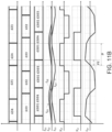
- FIG. 11B illustrates the key waveforms for AC-DC converter 1100 in FIG. 11A during a switching cycle of the power stage according to an embodiment of the present disclosure.
- the reference directions of currents and voltages in FIG. 11B correspond to the 60-degree segments of a line cycle when Va > 0, V B ⁇ 0, and Vc ⁇ 0.
- active switches S 1 and S 4 operate in a complementary fashion with a short dead time between the turn-on of one active switch and the turn-off of the other active switch.
- Active switches S 2 and S 3 operate in a complementary fashion as well.
- the duty cycles of active switches S 4 and S 2 are identical and smaller or equal to 50%.
- the gate signal of active switch S 2 has a 180-degree phase shift angle with respect to the gate signal of active switch S 4 .
- switches S O2 and S O3 have identical gate signals while switches S O1 and S O4 have identical gate signals.
- Switches S O1 and S O2 operate in a complementary fashion.
- the currents of boost inductors L 1 , L 2 , and L 3 are in DCM, where the currents reset in every switching cycle.
- a phase shift PS is introduced between the gate signal of active switch S 4 and the gate signal of switch Soi.
- the transformer primary side voltage V P is a typical three-level voltage, with a duty cycle D being determined by the duty cycle of active switch S 4 .
- the transformer current i Lr is a typical trapezoidal waveform.
- FIG. 12 shows an isolated three-phase ZVS PFC DCM AC-DC converter 1200 with an active full-bridge circuit 1230 on the primary side according to an embodiment of the present disclosure.
- Active full-bridge circuit 1230 includes active switches S 1 to S 4 , which replace half-bridge circuit 830 as shown in FIG.8A .
- the full-bridge AC points P and Q are connected to the primary side of a transformer 1240.
- a DC-link capacitor C DC is connected between the positive and negative terminals of the three-phase diode bridge.
- FIG. 13A illustrates an isolated three-phase ZVS PFC DCM AC-DC converter 1300 with an active full-bridge circuit 1330 and a blocking capacitor C B on the primary side according to an embodiment of the present disclosure.
- a blocking capacitor C B is inserted between active full-bridge circuit 1330 and a transformer 1340 to block the potential DC component to prevent saturation.
- FIG. 13B illustrates key waveforms for AC-DC converter 1300 in FIG. 13A during a switching cycle of the power stage according to an embodiment of the present disclosure.
- the reference directions of currents and voltages in FIG. 13B correspond to the 60-degree segments of a line cycle when Va > 0, V B ⁇ 0, and Vc ⁇ 0.
- active switches S 1 and S 2 operate in a complementary fashion with a short dead time between the turn-on of one active switch and the turn-off of the other active switch.
- Active switches S 1 and S 4 have identical gate signals while active switches S 2 and S 3 have identical gate signals.
- Switches S O2 and S O3 have identical gate signals while switches S O1 and S O4 have identical gate signals.
- the currents of boost inductors L 1 , L 2 , and L 3 are in DCM, where the currents reset in every switching cycle. A phase shift is introduced between the gate signal of active switch S 2 and the gate signal of switch Soi. Consequently, the transformer's primary side voltage V P has the same phase shift angle with respect to the secondary side voltage Vs.
- the transformer current i Lr is a typical trapezoidal waveform.
- FIG. 14 illustrates interleaved or paralleled isolated three-phase ZVS PFC DCM AC-DC converters according to an embodiment of the present disclosure.
- two converter modules 1401 and 1402 as shown in FIG. 8A can be paralleled or interleaved.
- the switching signals in each of converter modules 1401 and 1402 are the same as the switching signals shown in FIG. 8C .
- all of the switching signals in the second converter module 1402 are interleaved 180 degrees relative to the switching signals in the first converter module 1401.
- FIG. 15 illustrates an isolated three-phase ZVS PFC DCM AC-DC converter with two transformers TR1 and TR2 connected in series on the primary side and two separated outputs according to an embodiment of the present disclosure.
- the first primary side terminal of the first transformer TR1 is connected to the midpoint of two DC-link capacitors C DC1 and C DC2
- the second primary side terminal of the first transformer TR1 is connected to the first primary side terminal of the second transformer TR2.
- the second primary side terminal of the second transformer TR2 is connected to the midpoint of the two active switches S 1 and S 2 .
- the secondary side of the first transformer TR1 is coupled to a full active bridge for the first output, while the secondary side of the second transformer TR2 is coupled to another full active bridge for the second output.
- FIG. 16 illustrates an isolated three-phase ZVS PFC DCM AC-DC converter with two transformers TR1 and TR2 connected in series on the primary side and connected in parallel on the secondary side according to an embodiment of the present disclosure. As shown in FIG. 16 , because the secondary sides of transformers TR1 and TR2 are connected in parallel, only one full active bridge is implemented.
- FIG. 17A illustrates an isolated three-phase ZVS PFC DCM AC-DC converter 1700, having low input-current harmonic, with two half-bridge modules 1731 and 1732 according to an embodiment of the present disclosure.
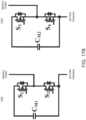
- FIG. 17B illustrates an enlarged view of half-bridge modules 1731 and 1732 of AC-DC converter 1700 in FIG. 17A .
- AC-DC converter 1700 includes three boost inductors L 1 , L 2 , and L 3 coupled through an EMI filter 1710 to three-phase input voltage terminals V A , V B , and Vc, and three capacitors C 1 , C 2 , and C 3 connected in the Y or star configuration.
- Boost inductors L 1 , L 2 , and L 3 are followed by a three-phase diode bridge 1720 and a switching converter stage 1730.
- Switching converter stage 1730 includes two half-bridge modules 1731 and 1732. As shown in FIG. 17B , half-bridge module 1731 includes two active switches S 1 and S 2 connected in series and coupled to a capacitor C M1 to form a loop. Likewise, half-bridge module 1732 includes two active switches S 3 and S 4 connected in series and coupled to a capacitor C M2 to form a loop. Referring to FIGs. 17A and 17B , the middle point of half-bridge module 1731 is connected to the positive terminal POS of the three-phase diode bridge 1720 and the bottom terminal of half-bridge module 1731 is connected to the middle point of half-bridge module 1732. The bottom terminal of half-bridge module 1732 is connected to the negative terminal NEG of the three-phase diode bridge 1720.
- a common point N of input filter capacitors C 1 , C 2 , and C 3 is connected to the bottom terminal of half-bridge module 1731, and one primary side terminal of transformer 1740.
- the midpoint M of two DC-link capacitors C DC1 and C DC2 is connected to the other primary terminal of transformer 1740.
- a full active bridge 1750 is connected to the secondary side of transformer 1740.
- the Y-connected capacitors C 1 , C 2 , and C 3 create a virtual ground, a node with the same voltage potential as the input voltage source neutral common point (or neutral terminal) N, which is not physically available in a three-wire system.
- This common point N is directly connected to the midpoint between two half-bridge modular circuits (i.e., half-bridge modules 1731 and 1732), and the three input currents are decoupled with each other. Due to this decoupling, the current in each of the three boost inductors L 1 , L 2 , and L 3 is now dependent only on the corresponding input phase voltage, which results in low THD and a high power factor.
- AC-DC converter 1700 can further include a controller 1760 to provide switching signals to active switches S 1 , S 2 , S 3 , S 4 at primary side (i.e., the primary side switches), and switches S O1 , S O2 , S O3 , S O4 at secondary side (i.e., the secondary side switches).
- the switching signals for active switches S 1 and S 4 are identical and the switching signals for active switches S 2 and S 3 are identical.
- the switching signals can be fixed at a duty cycle of substantially 50% and the switching signals of the two active switches in each of the half-bridge modules 1731, and 1732 are complementary.
- the switching signals may provide a small dead time where each pair of the active switches is turned off slightly before the opposite pair is turned on, such that all active switches S 1 , S 2 , S 3 , S 4 are briefly off during the dead time.
- active switches S 1 and S 4 are turned on, it can be seen that common point N is connected to the negative terminal NEG of three-phase diode bridge 1720, that active switch S 3 is blocking the voltage of capacitor C M2 , and that capacitor C M1 becomes a DC-link capacitor.
- the switching signals for switches S O1 and S O4 are identical and the switching signals for switches S O2 and S O3 are identical.
- the switching signals can be fixed at a duty cycle of substantially 50% and the switching signals of switches S O1 and S O2 are complementary.
- the switching frequencies of all switches are identical.
- a phase shift angle may be introduced between the switching signal of active switch S 4 and the switching signal of switch Soi.
- controller 1760 can be adapted to vary the switching frequency of all switches and the phase shift angle based on at least one of the input three-phase voltage, the input three-phase current, the DC-link capacitor voltages, the output voltage, and the output current. Any suitable device may be used to measure the voltages or currents that the controller 1760 uses for control (e.g., analog to digital converter, current to voltage converter, etc.). The minimum switching frequency is determined by the full load and minimum input voltage, while the maximum switching frequency is determined by the light load and maximum input voltage. To avoid a very high-frequency operation, if AC-DC converter 1700 is required to operate at a very light load or even no load, a controlled burst mode or pulse skip mode can be implemented.
- Pulse width modulation control is another possible control scheme in this converter, but realizing ZVS at full load range is not feasible.
- the switching frequency may be determined by controller 1760 from the sensed values in any suitable way.
- Ref. [4] describes variable frequency control that may be used in some embodiments.
- One challenge of the operation of the circuit shown in FIG. 17A is to balance the voltage of the flying capacitors C M1 and C M2 of half-bridge modules 1731 and 1732.
- Controller 1760 can change the duty cycle of active switches S 1 , S 2 , S 3 , and S 4 when any unbalanced voltage is detected.
- a relatively larger capacitance is preferred for capacitors C M1 and C M2 in half-bridge modules 1731 and 1732 to make it less likely to suffer voltage imbalance during the operation.
- AC-DC converter 1700 offers a low THD of the input current and a high power factor along with ZVS of the switches by operating the boost inductors in DCM and by implementing the variable-frequency modulation and phase shift modulation control strategy.
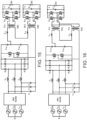
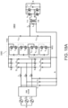
- FIG. 18A shows an implementation in a high-voltage application.
- Each diode in the three-phase diode bridge 1720 in FIG. 17A is replaced by m diodes connected in series to block the high input voltage.
- a passive snubber circuit may be required to balance the blocking voltage for each diode.
- a total of 2n half-bridge modules are implemented.
- the middle point of every half-bridge module is connected to the bottom terminal of the previous half-bridge module ("cascaded").
- the middle point of the first half-bridge module is connected to the positive terminal POS of the three-phase diode bridge and the bottom terminal of the last half-bridge module is connected to the negative terminal NEG of the three-phase diode bridge.
- the common point N of the input filter capacitors C 1 , C 2 , and C 3 is connected to the midpoint between the upper n half-bridge modules and the lower n half-bridge modules, and also to one primary side terminal of the transformer TR.
- FIG. 18B illustrates the key waveforms of AC-DC converter 1800 in FIG. 18A during a switching cycle according to an embodiment of the present disclosure.
- the control signals of active switches S 1a , S 2a , ... , S na are identical to the control signals of active switches S (n+1)b , S (n+2)b , ... , S 2nb , which are fixed at a duty cycle of substantially 50%.
- the control signals of active switches S 1b , S 2b , ... , S nb are identical to the control signals of active switches S (n+1)a , S (n+2)a , ... , S 2na , which are also fixed at a duty cycle of substantially 50%.
- the control signals of the two active switches of each half-bridge module are complementary.
- the top active switch of each half-bridge module in the top half leg and the bottom active switch of each half-bridge module in the bottom half leg are turned on and off simultaneously.
- the bottom active switch of each half-bridge module in the top half leg and the top active switch of each half-bridge module in the bottom half leg are turned on and off simultaneously.
- the voltage of each capacitor in each half-bridge module is only 1/n of the total DC bus voltage and each active switch only needs to block 1/n of the total DC bus voltage, which makes it possible to use low voltage active switches in very high input and output voltage applications.
- the voltages of all capacitors in half-bridge modules may be sensed.
- a controller can change the duty cycle of the active switches when any voltage unbalances are detected.
- a relatively larger capacitance is preferred in the half-bridge module to make it less likely to suffer voltage imbalance during the operation.
- the switching signals can be fixed at a duty cycle of substantially 50%.
- the switching signals of S O1 and S O2 are complementary, and so are the switching signals of S O3 and S O4 .
- a phase shift angle can be introduced between the switching signal of active switches S 1a to S na and the switching signal of switch Soi.
- the additional 2n half-bridge modules are connected in the same fashion as the existing 2n half-bridge modules and they are coupled between the positive terminal and the negative terminal of the three-phase diode bridge.
- the circuit further includes a transformer followed by a full active bridge.
- the two sets of 2n half-bridge modules behave like the switching converter stage 1830 as shown in FIG. 18A .
- FIG. 20A illustrates a three-phase three-level flying capacitor ZVS PFC DCMAC-DC converter 2000, having low input-current harmonic, with four half-bridge modules according to an embodiment of the present disclosure.
- AC-DC converter 2000 includes three boost inductors L 1 , L 2 , and L 3 coupled through an EMI filter 2010 to three-phase input voltage terminals V A , V B , and Vc, and three capacitors C 1 , C 2 , and C 3 connected in the Y or star configuration.
- Boost inductors L 1 , L 2 , and L 3 are followed by a three-phase diode bridge 2020 and a switching converter stage 2030.
- Switching converter stage 2030 includes four half-bridge modules, wherein each half-bridge module includes two active switches in series and then coupled with a capacitor.
- One terminal of a flying or floating capacitor Cf is connected to the bottom terminal of the first half-bridge module and the other terminal of the flying capacitor Cf is connected to the bottom terminal of the third half-bridge module.
- FIG. 20B illustrates the key waveforms of AC-DC converter 2000 in FIG. 20A during a switching cycle of the power stage according to an embodiment of the present disclosure.
- the reference directions of currents and voltages in FIG. 20B correspond to the 60-degree segments of a line cycle when Va > 0, V B ⁇ 0, and Vc ⁇ 0.
- the two active switches in each half-bridge module operate in a complementary fashion with a short dead time between the turn-on of one switch and turn-off of the other switch.
- the duty cycle of active switches S 4b and S 2b are identical and smaller or equal to 50%.
- the gate signal of active switch S 2b has a 180-degree phase shift angle respecting the gate signal of active switch S 4b .
- switches S O2 and S O3 have identical gate signals while switches S O1 and S O4 have identical gate signals.
- Switches S O1 and S O2 operate in a complementary fashion.
- the boost inductor currents are in DCM, where the currents reset in every switching cycle.
- a phase shift PS is introduced between the gate signal of active switch S 4b and the gate signal of switch Soi.
- the transformer's primary side voltage V P is a typical three-level voltage, and duty cycle D is determined by the duty cycle of active switch S 4b .
- the transformer current i Lr is a typical trapezoidal waveform.
- each half-bridge module in switching converter stage 2030 of FIG. 20A is replaced by n number of half-bridge modules connected in a way as shown in FIG. 18A to block high voltage.
- two transformers TR1 and TR2 are coupled to the primary side circuit of FIG. 18A .
- the two transformers' primary sides and the primary side circuit are connected in the same way as shown in FIG. 18A . In other words, the two transformers' primary sides are connected in parallel.
- each transformer is coupled with a full active bridge and an individual load.
- the primary side voltages of both transformers are identical and determined by the primary side operations. However, the output power and voltage of each output port can be individually controlled by the corresponding secondary side active bridge.
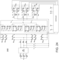
- FIG. 22B illustrates key waveforms of AC-DC converter 2200 in FIG. 22A during a switching cycle of the power stage according to an embodiment of the present disclosure.
- the active switches at primary side i.e., primary side switches
- switches S O2 and S O3 have identical gate signals while switches S O1 and S O4 have identical gate signals.
- Switches S O1 and S O2 operate in a complementary fashion with a 50% duty cycle.
- Switches S O6 and S O7 have identical gate signals, while switches Sos and Sos have identical gate signals. Switches Sos and S O6 operate in a complementary fashion with a 50% duty cycle.
- phase shift between active switch S 1a and switch S O1 is PS1, while the phase shift between S 1a and Sos is PS2. Due to the different phase shift angles and output voltage, the currents of the two transformers TR1 and TR2 are different. Consequently, the power of each output port can be controlled individually.
- N transformers are coupled to the primary-side switching converter stage as shown in FIG. 22 .
- Each transformer is followed by a full active bridge and a load.
- Each output current, voltage, and power are separately controlled by the phase shift angle between the transformer primary side voltage and the transformer secondary side voltage.
- a total of N transformers are coupled to the primary-side switching converter stage as shown in FIG. 21 .
- Each transformer is followed by a full active bridge and a load.
- Each output current, voltage, and power are separately controlled by the phase shift angle between the transformer primary side voltage and the transformer secondary side voltage.
Landscapes
- Engineering & Computer Science (AREA)
- Power Engineering (AREA)
- Physics & Mathematics (AREA)
- Electromagnetism (AREA)
- Rectifiers (AREA)
Abstract
A three-phase AC-DC converter (800) is provided that can offer a low total harmonic distortion (THD) of input current and good power factor with the capability of soft-switching of the active switches (S1, S2). In one aspect, a phase shift (PS) is introduced to the gate signal of one of the primary side active switches (S2) of the three-phase AC-DC converter (800) and the gate signal of a corresponding one of the secondary side active switches (SO1) of the three-phase AC-DC converter (800).
Description
- The present disclosure relates to a multi-phase AC-DC converter. More particularly, the present disclosure relates to a three-phase AC-DC converter with power-factor correction (PFC).
- Generally, a front-end power-factor-correction (PFC) rectifier is required in three-phase AC-DC applications. The PFC rectifier usually provides low total harmonic distortion (THD) of the input three-phase current and a high power factor.
-
FIG. 1 illustrates a conventional three-phase rectifier with only one switch. This three-phase rectifier performs PFC and achieves low THD by operating the boost inductors in the discontinuous conduction mode (DCM), where the boost inductors are completely discharged in every switching cycle. In the DCM operation, the line current naturally follows the line voltage resulting in improved THD and power factor (PF). Because the inductor current is not controlled directly, usually low-bandwidth constant switching frequency control is implemented. As reported in related literature, the three-phase rectifier is capable of achieving 10% to 20% THD, which is acceptable in some applications. - To further minimize the current distortion in high-power applications, the Vienna rectifier illustrated in
FIG. 2 is proposed in Ref. [1]. Vienna rectifier offers high-efficiency AC-DC conversion, low THD of input current, and a high power factor, but the Vienna rectifier includes too many components and is thus not attractive in low-cost applications. -
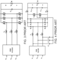
FIG. 3 illustrates a six-switch boost converter with the capability for bidirectional power flow. By using wide-band-gap devices, e.g., SiC devices, it can provide both high efficiency and high power density as reported in Ref. [2]. The high cost of wide-band-gap devices is a potential obstacle for this converter to be widely accepted. -
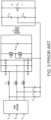
FIG. 4 illustrates a two-switch three-phase rectifier proposed in Ref. [3]. By connecting the capacitors C1, C2, and C3 in the "Y" connection, a virtual neutral point is obtained. The virtual neutral point is further connected to the midpoint of the two switches and the midpoint of the output capacitors, CO1 and CO2. This connection partially decouples the phase currents for most of the line period by making the three-phase PFC rectifier operate as three independent single-phase PFC rectifiers. This structure is further improved as illustrated inFIG. 5 , which is proposed in Ref. [4]. The rectifier inFIG. 5 provides better electromagnetic interference (EMI) performance by adding an inductively decoupling stage, which makes it suitable in fast high-voltage change applications. - Recently, high input voltage three-phase power supplies are more and more attractive in high power applications, e.g., solid-stage-transformer, because they can deliver more power for the same amount of input current. To operate the converters in
FIGs. 1 through 5 in high input voltage conditions, one possible approach is to directly replace the low voltage devices with ultra-high voltage devices as reported in Ref. [5]. However, ultra-high voltage devices are currently not available in the market and will be very costly in near future. Another possible approach is to cascade the front-end bridges to block the high input voltage as reported in Ref. [6]. This approach usually requires a substantial amount of active switches for the front-end PFC and also needs multiple DC-DC converters to provide galvanic isolation, which further increases the number of switches for the system. - Many power conversion applications (e.g., battery charging in electrical vehicles (EVs)) require a regulated output voltage over a wide voltage range. For example, a typical EV battery charger circuit has a voltage range between 240 volts to 460 volts. Thus, a converter that can provide both PFC and a regulated output voltage over a very wide output voltage range is desired to accommodate the charging requirements at different battery voltage levels. An overview of Dual-Active-Bridge (DAB) Isolated Bidirectional DC-DC Converters as illustrated in
FIG. 6 is discussed in Ref. [7], where DAB is used in DC-DC conversion for a wide voltage gain range. Ref. [8] further improved the conventional DAB to feature multi-port functions, such as the triple-active-bridge (TAB) DC-DC isolated converter as illustrated inFIG. 7 . However, a separated AC-DC converter is required before the DAB stage to provide PFC function. A simpler structure is desired. -
- Ref. [1]: J. W. Kolar and F.C. Zach, "A novel three-phase utility interface minimizing line current harmonics of high-power telecommunications rectifier modules," IEEE Transactions on Industrial Electronics, vol. 44, no. 4, pp. 456-467, Aug. 1997.
- Ref. [2]: J.W. Kolar and T. Friedli, "The essence of three-phase PFC rectifier systems," IEEE Trans. Power Electron., vol. 28, no. 1, pp. 176-198, Jan. 2013.
- Ref. [3]:
Jianping Ying et al., "Integrated Converter Having Three-Phase Power Factor Correction," U.S. Pat. No. 7,005,759, issued February 28, 2006 . - Ref. [4]:
Yungtaek Jang et al., "Three-Phase Soft-Switched PFC Rectifiers," U.S. Pat. No. 8,687,388, issued April 1, 2014 . - Ref. [5]: Madhusoodhanan et al., "Solid-State Transformer and MV Grid Tie Applications Enabled by 15 kV SiC IGBTs and 10 kV SiC MOSFETs Based Multilevel Converters," IEEE Transactions on Industry Applications, vol. 51, no. 4, pp. 3343-3360, July-Aug. 2015.
- Ref. [6]: X. She, A.Q. Huang and R. Burgos, "Review of Solid-State Transformer Technologies and Their Application in Power Distribution Systems," IEEE Journal of Emerging and Selected Topics in Power Electronics, vol. 1, no. 3, pp. 186-198, Sept. 2013.
- Ref. [7]: B. Zhao, Q. Song, W. Liu, and Y Sun, "Overview of Dual-Active-Bridge Isolated Bidirectional DC-DC Converter for High-Frequency-Link Power-Conversion System," in IEEE Transactions on Power Electronics, vol. 29, no. 8, pp. 4091-4106, Aug. 2014.
- Ref. [8]: C. Zhao, S. D. Round and J. W. Kolar, "An Isolated Three-Port Bidirectional DC-DC Converter With Decoupled Power Flow Management," in IEEE Transactions on Power Electronics, vol. 23, no. 5, pp. 2443-2453, Sept. 2008.
- In one aspect, the present disclosure provides an AC/DC converter comprising: a plurality of internal terminals including a positive terminal, a negative terminal, and a neutral terminal; an input stage electrically coupled to the positive, negative, and neutral terminals and including at least three input terminals that are connectable to a three-phase AC power source; a switching converter stage including a plurality of primary side switches electrically coupled between the positive and negative terminals; an output stage electrically coupled to the switching converter stage and the neutral terminal, the output stage including output terminals that are connectable to a load, thereby providing a DC voltage to the load, wherein the output stage comprises a transformer and an active bridge including a plurality of secondary side switches; and a controller electrically coupled to the switching converter stage and the output stage to generate gate signals for the plurality of primary side switches and the plurality of secondary side switches, wherein a phase shift is introduced between the gate signal of one of the plurality of primary side switches and the gate signal of a corresponding one of the plurality of secondary side switches.
- In one embodiment, the plurality of primary side switches of the switching converter stage comprises two active switches and wherein a midpoint of the two active switches is electrically coupled to the neutral terminal.
- In one embodiment, the input stage comprises a three-phase diode bridge.
- In one embodiment, the AC/DC converter further comprises a plurality of boost inductors, each being electrically coupled between a corresponding input terminal of the three-phase AC power source through an EMI filter and a corresponding leg of the three-phase diode bridge.
- In one embodiment, the AC/DC converter further comprises a plurality of capacitors, each being connected between a corresponding input terminal of the three-phase AC power source through an EMI filter and the neutral terminal.
- In one embodiment, the switching converter stage further comprises a plurality of DC-link capacitors connected in series and coupled to the input stage in parallel.
- In one embodiment, a midpoint of the plurality of DC-link capacitors is electrically coupled to one primary side terminal of the transformer, while a midpoint of the plurality of primary side switches is electrically coupled to another primary side terminal of the transformer.
- In one embodiment, the output stage comprises: a first transformer and a first active bridge connected to a secondary side of the first transformer, and a second transformer and a second active bridge connected to a secondary side of the second transformer. A first primary side terminal of the first transformer is connected to a midpoint of the plurality of DC-link capacitors. A second primary side terminal of the first transformer is connected to a first primary side terminal of the second transformer. A second primary side terminal of the second transformer is connected to the neutral terminal.
- In one embodiment, the primary and secondary side switches are metal-oxide-semiconductor field-effect transistors (MOSFETs) or insulated gate bipolar transistors (IGBTs) with antiparallel diodes.
- In one embodiment, the AC/DC converter further comprises a blocking capacitor electrically coupled between one of secondary side terminals of the transformer and a midpoint of the active bridge.
- In one embodiment, the active bridge comprises a full active bridge including four active switches or a half bridge including two active switches.
- In one embodiment, the switching converter stage comprises first, second, third, and fourth active switches electrically coupled in series and a flying capacitor electrically coupled between a midpoint between the first and second active switches and a midpoint between the third and fourth active switches. A midpoint of the second and third active switches is electrically coupled to the neutral terminal.
- In one embodiment, the switching converter stage comprises an active full-bridge circuit including first and second active switches electrically coupled in series between the positive and negative terminals, and third and fourth active switches electrically coupled in series between the positive and negative terminals. A midpoint between the first and second active switches is electrically coupled to the neutral terminal, and a midpoint between the third and fourth active switches is electrically coupled to one primary side terminal of the transformer.
- In one embodiment, the AC/DC converter further comprises a DC-link capacitor electrically coupled to the input stage in parallel.
- In one embodiment, the AC/DC converter further comprises a blocking capacitor electrically coupled between said midpoint between the third and fourth active switches and said one primary side terminal of the transformer.
- In one embodiment, the output stage comprises two transformers connected in series on a primary side of said two transformers and connected in parallel on a secondary side of said two transformers.
- In one aspect, the present disclosure provides an interleaved or paralleled AC/DC converter comprising two of the AC/DC converters. In a directly parallel operation, the gate signals for a first one of the AC/DC converters are the same as the gate signals for a second one of the AC/DC converters. In an interleaved operation, the gate signals in the first one of the AC/DC converters are interleaved 180 degrees relative to the gate signals in the second one of the AC/DC converters.
- In one aspect, the present disclosure provides an AC/DC converter comprising: a plurality of internal terminals including a positive terminal, a negative terminal, and a neutral terminal; an input stage electrically coupled to the positive, negative, and neutral terminals and including at least three input terminals that are connectable to a three-phase AC power source; a switching converter stage including a plurality of half-bridge modules, each half-bridge module including a capacitor and first and second active switches serially connected to form a loop, wherein a first one of the plurality of half-bridge modules is electrically coupled to the positive terminal, a second one of the plurality of half-bridge modules is electrically coupled to the negative terminal, and at least two of the plurality of half-bridge modules are electrically coupled to the neutral terminal; an output stage electrically coupled to the switching converter stage and the neutral terminal, the output stage including output terminals that are connectable to a load, thereby providing a DC voltage to the load, wherein the output stage comprises a transformer and an active bridge including a plurality of secondary side switches; and a controller coupled to the switching converter stage and the output stage to generate gate signals for the first and second active switches of the plurality of half-bridge modules and the plurality of secondary side switches, wherein a phase shift is introduced between the gate signal of one of the first and second active switches of the plurality of half-bridge modules and the gate signal of a corresponding one of the plurality of secondary side switches.
- In one embodiment, the switching converter stage further comprises a plurality of DC-link capacitors connected in series and coupled to the input stage in parallel.
- In one embodiment, a midpoint of the plurality of DC-link capacitors is electrically coupled to one primary side terminal of the transformer.
- In one embodiment, the input stage comprises a three-phase diode bridge.
- In one embodiment, the plurality of half-bridge modules of the switching converter stage comprises first and second half-bridge modules, wherein a midpoint of the first and second active switches of the first half-bridge module is connected the positive terminal. A connection point between the capacitor and the second active switch of the first half-bridge module is connected to a midpoint of the first and second active switches of the second half-bridge module and the neutral terminal. A connection point between the capacitor and the second active switch of the second half-bridge module is connected to the negative terminal.
- In one embodiment, the plurality of half-bridge modules of the switching converter stage comprises a total of 2n half-bridge modules, and n is a positive integer. A middle point between the first and second active switches of each one of the 2n half-bridge modules is connected to a bottom terminal between the capacitor and the second active switch of a previous one of the 2n half-bridge module, except that the middle point between the first and second active switches of a first one of the 2n half-bridge modules is connected to the positive terminal and that the bottom terminal between the capacitor and the second active switch of a last one of the 2n half-bridge modules is connected to the negative terminal. The neutral terminal is connected to a midpoint between upper n half-bridge modules and lower n half-bridge modules of the 2n half-bridge modules.
- In one embodiment, the input stage comprises a total of 6m diodes, the plurality of half-bridge modules of the switching converter stage comprises two sets of 2n half-bridge modules, and m and n are positive integers. A first set of the 2n half-bridge modules is cascaded between the positive and negative terminals with the neutral terminal being electrically coupled to a midpoint between upper n half-bridge modules and lower n half-bridge modules of the first set of the 2n half-bridge modules. A second set of the 2n half-bridge modules is cascaded between the positive and negative terminals with one primary side terminal of the transformer being connected to a midpoint between upper n half-bridge modules and lower n half-bridge modules of the second set of the 2n half-bridge modules.
- In one embodiment, the switching converter stage comprises first, second, third, and fourth half-bridge modules cascaded between the positive and negative terminals and a flying capacitor, wherein a first terminal of the flying capacitor is connected to a bottom terminal between the capacitor and the second active switch of the first half-bridge module, and a second terminal of the flying capacitor is connected to a bottom terminal between the capacitor and the second active switch of the third half-bridge module.
- In one embodiment, the input stage comprises a total of 6m diodes, the switching converter stage comprises a total of 4n half-bridge modules cascaded between the positive and negative terminals and a flying capacitor, and m and n are positive integers, wherein the neutral terminal is electrically coupled to a midpoint between upper 2n half-bridge modules and lower 2n half-bridge modules of the 4n half-bridge modules, and wherein the flying capacitor is connected between a first midpoint between upper n half-bridge modules and lower n half-bridge modules of said upper 2n half-bridge modules and a second midpoint between upper n half-bridge modules and lower n half-bridge modules of said lower 2n half-bridge modules.
- In one embodiment, the output stage comprises a first transformer and a second transformer, wherein a primary side of the first transformer is connected in parallel with a primary side of the second transformer, and wherein each of the first and second transformers is independently connected to a full active bridge on a secondary side.
- In one embodiment, the output stage comprises a total of N transformers, primary sides of the N transformers are connected in parallel with each other, and wherein a secondary side of each of the N transformers is independently connected to a full active bridge.
- In one embodiment, the switching converter stage comprises a total of 4n half-bridge modules cascaded between the positive and negative terminals and a flying capacitor, and n is a positive integer, wherein the neutral terminal is electrically coupled to a midpoint between upper 2n half-bridge modules and lower 2n half-bridge modules of the 4n half-bridge modules, wherein the flying capacitor is connected between a first midpoint between upper n half-bridge modules and lower n half-bridge modules of said upper 2n half-bridge modules and a second midpoint between upper n half-bridge modules and lower n half-bridge modules of said lower 2n half-bridge modules, wherein the output stage comprises a total of N transformers, primary sides of the N transformers are connected in parallel with each other, and a secondary side of each of the N transformers is independently connected to a full active bridge.
- The present disclosure is better understood upon consideration of the following detailed description and the accompanying figures.
-
FIG. 1 illustrates a conventional three-phase single-switch PFC DCM boost rectifier circuit. -
FIG. 2 illustrates a conventional three-phase Vienna PFC rectifier circuit. -
FIG. 3 illustrates a conventional three-phase six-switch PFC boost rectifier circuit. -
FIG. 4 illustrates a conventional three-phase two-switch PFC DCM boost rectifier circuit with virtual neutral and with split output capacitors. -
FIG. 5 illustrates a conventional three-phase two-switch zero voltage switching (ZVS) PFC DCM boost rectifier circuit. -
FIG. 6 illustrates a conventional dual-active-bridge (DAB) DC-DC isolated converter. -
FIG. 7 illustrates a conventional triple-active-bridge (TAB) DC-DC isolated converter with two isolated outputs. -
FIG. 8A illustrates an isolated three-phase ZVS PFC DCM AC-DC converter according to an embodiment of the present disclosure. -
FIG. 8B illustrates the AC-DC converter ofFIG. 8A coupled with a controller, according to an embodiment of the present disclosure. -
FIG. 8C illustrates key waveforms for the AC-DC converter ofFIG. 8A during a switching cycle according to an embodiment of the present disclosure. -
FIG. 9 illustrates an isolated three-phase ZVS PFC DCM AC-DC converter with a blocking capacitor at the secondary side according to an embodiment of the present disclosure. -
FIG. 10 illustrates an isolated three-phase ZVS PFC DCM AC-DC converter with an active half-bridge circuit at the secondary side of the transformer according to an embodiment of the present disclosure. -
FIG. 11A illustrates an isolated three-phase three-level flying capacitor ZVS PFC DCM AC-DC converter according to an embodiment of the present disclosure. -
FIG. 11B illustrates key waveforms of the AC-DC converter inFIG. 11A during a switching cycle according to an embodiment of the present disclosure. -
FIG. 12 illustrates an isolated three-phase ZVS PFC DCM AC-DC converter with an active full-bridge circuit on the primary side according to an embodiment of the present disclosure. -
FIG. 13A illustrates an isolated three-phase ZVS PFC DCM AC-DC converter with an active full-bridge circuit and a blocking capacitor on the primary side according to an embodiment of the present disclosure. -
FIG. 13B illustrates key waveforms of the AC-DC converter inFIG. 13A during a switching cycle according to an embodiment of the present disclosure. -
FIG. 14 illustrates interleaved or paralleled isolated three-phase ZVS PFC DCM AC-DC converters according to an embodiment of the present disclosure. -
FIG. 15 illustrates an isolated three-phase ZVS PFC DCM AC-DC converter with two transformers connected in series on the primary side and two separated outputs according to an embodiment of the present disclosure. -
FIG. 16 illustrates an isolated three-phase ZVS PFC DCM AC-DC converter with two transformers connected in series on the primary side and connected in parallel on the secondary side according to an embodiment of the present disclosure. -
FIG. 17A illustrates an isolated three-phase ZVS PFC DCM AC-DC converter with two half-bridge modules according to an embodiment of the present disclosure. -
FIG. 17B illustrates an enlarged view of the half-bridge modules of the AC-DC converter inFIG. 17A . -
FIG. 18A illustrates a generalized isolated three-phase ZVS PFC DCMAC-DC converter based on a total of 6m (m = 1, 2, 3, ... ) diodes and 2n (n = 1, 2, 3, ... ) half-bridge modules according to an embodiment of the present disclosure. -
FIG. 18B illustrates the key waveforms of the AC-DC converter inFIG. 18A during a switching cycle according to an embodiment of the present disclosure. -
FIG. 19 illustrates a generalized isolated three-phase ZVS PFC DCM AC-DC converter based on a total of 6m (m = 1, 2, 3, ... ) diodes and two sets of 4n (n = 1, 2, 3, ... ) half-bridge modules with both frequency controller and phase-shift controller according to an embodiment of the present disclosure. -
FIG. 20A illustrates a three-phase three-level flying capacitor ZVS PFC DCM AC-DC converter with four half-bridge modules according to an embodiment of the present disclosure. -
FIG. 20B illustrates the key waveforms of the AC-DC converter inFIG. 20A during a switching cycle according to an embodiment of the present disclosure. -
FIG. 21 illustrates a generalized isolated three-phase flying capacitor ZVS PFC DCM boost rectifier circuit based on a total of 6m (m = 1, 2, 3, ... ) diodes and a total of 4n (n = 1, 2, 3, ... ) half-bridge modules according to an embodiment of the present disclosure. -
FIG. 22A illustrates a generalized isolated three-phase ZVS PFC DCMAC-DC converter based on a total of 6m (m = 1, 2, 3, ... ) diodes and 2n (n = 1, 2, 3, ... ) half-bridge modules with two isolated outputs according to an embodiment of the present disclosure. -
FIG. 22B illustrates key waveforms of the AC-DC converter inFIG. 22A during a switching cycle according to an embodiment of the present disclosure. -
FIG. 23 illustrates a generalized isolated three-phase ZVS PFC DCM AC-DC converter based on a total of 6m (m = 1, 2, 3, ... ) diodes and 2n (n = 1, 2, 3, ...) half-bridge modules with N isolated outputs according to an embodiment of the present disclosure. -
FIG. 24 illustrates a generalized isolated three-phase three-level flying capacitor ZVS PFC DCMAC-DC converter based on a total of 6m (m = 1, 2, 3, ... ) diodes and 4n (n = 1, 2, 3, ... ) half-bridge modules with N isolated outputs according to an embodiment of the present disclosure. - The inventors have recognized and appreciated the need for a low-cost, low input-current harmonic, and high power factor three-phase isolated AC-DC converter with high scalability for high input voltage and high power applications. The present disclosure relates to a three-phase AC-DC converter, which offers a very low THD of the input current and a good power factor with the capability of soft-switching of the active switches.
-
FIG. 8A shows an isolated three-phase zero-voltage switching (ZVS), power-factor-correction (PFC), discontinuous-conduction mode (DCM) AC-DC converter 800, having low input-current harmonic, according to an embodiment of the present disclosure. The AC-DC converter 800 includes three boost inductors L1, L2, and L3 coupled through anEMI filter 810 to three-phase input voltage terminals VA, VB, and Vc, and three capacitors C1, C2, and C3 connected in a "Y" or star configuration. Each of capacitors C1, C2, and C3 is connected to a corresponding one of three-phase input voltage terminals VA, VB, and Vc through anEMI filter 810. - Boost inductors L1, L2, and L3 are followed by a three-
phase diode bridge 820 and a half-bridge circuit 830. Half-bridge circuit 830 includes two active switches S1 and S2, serially connected between the positive terminal POS and the negative terminal NEG of three-phase diode bridge 820, where the midpoint of the two active switches S1 and S2 is connected to a connection point (i.e., neutral point or neutral terminal) Y of capacitors C1, C2, and C3. - Two serially connected DC-link capacitors CDC1 and CDC2 are coupled to three-
phase diode bridge 820 in parallel, i.e., between positive and negative terminals POS, and NEG. The midpoint of the two DC-link capacitors CDC1 and CDC2 is connected to one primary side terminal oftransformer 840, while the midpoint of active switches S1 and S2 is connected to the other primary side terminal oftransformer 840. - A full
active bridge 850 including switches SO1, SO2, SO3, and SO4 is connected to the secondary side oftransformer 840. It is appreciated that active switches S1 and S2 and switches SO1, SO2, SO3, and SO4 may be any suitable switch, such as a metal-oxide-semiconductor field-effect transistor (MOSFET), an insulated gate bipolar transistor (IGBT) with an antiparallel diode, and the like. -
FIG. 8B illustrates AC-DC converter 800 ofFIG. 8A coupled with acontroller 860, according to an embodiment of the present disclosure.Controller 860 obtains information from the DC-link of three-phase diode bridge 820 (e.g., DC-link voltage) and/or from the output of full active bridge 850 (e.g., output current, output voltage, and output power). Based on the information, thecontroller 860 adjusts control variables, such as the switching frequency and the phase shift between active switches S1 and S2 at primary side, and switches SO1, SO2, SO3, and SO4 at secondary side, to regulate the DC-link voltage, output voltage, output current, and output power. -
FIG. 8C illustrates key waveforms for AC-DC converter 800 ofFIG. 8A during a switching cycle according to an embodiment of the present disclosure. The reference directions of currents and voltages inFIG. 8C corresponds to the 60-degree segments of a line cycle when Va > 0, VB < 0, and Vc < 0 (VA, VB and Vc represent the voltages at the input voltage terminals VA, VB and Vc respectively). As shown inFIG. 8C , active switches S1 and S2 operate in a complementary fashion with a short dead time between the turn-on of one active switch and the turn-off of the other active switch. In addition, switches SO2 and SO3 have identical gate signals, while switches SO1 and SO4 have identical gate signals. The boost inductor currents iL1, iL2, and iL3 are in the discontinuous conduction mode (DCM) because the currents are reset to zero in every switching cycle. A phase shift PS is introduced between the gate signal of active switch S2 and the gate signal of switch Soi. Consequently, the primary side voltage VP oftransformer 840 has the same phase shift angle as the secondary side voltage Vs oftransformer 840. The transformer current iLr has a typical trapezoidal waveform as that in a conventional DAB converter. -
FIG. 9 illustrates an isolated three-phase ZVS PFC DCM AC-DC converter 900 with a blocking capacitor CB at the secondary side. Blocking capacitor CB is connected between one of the secondary side terminals oftransformer 940 and a midpoint of a half-bridge circuit (including switches Soi and SO3) at the secondary side. Blocking capacitor CB blocks the potential DC component from the secondary side full bridge (including switches Soi, SO2, SO3, and SO4) so that the secondary side oftransformer 940 does not suffer saturation. - In an alternative embodiment, the secondary side active full-bridge circuit of AC-
DC converter 900 inFIG. 9 can be replaced by a typical half-bridge circuit to further reduce the number of active components.FIG. 10 illustrates an isolated three-phase ZVS PFC DCMAC-DC converter 1000 with an active half-bridge circuit at the secondary side oftransformer 1040 according to an embodiment of the present disclosure. The operation of AC-DC converter 1000 inFIG. 10 is very similar to AC-DC converter 800 inFIG. 8 . The primary side voltage VP oftransformer 1040 has a controllable phase shift angle with respect to secondary side voltage Vs. Transformer current iLr is a typical trapezoidal waveform as that in a conventional DAB converter. -
FIG. 11A illustrates an isolated three-phase three-level ZVS PFC DCM AC-DC converter 1100 according to an embodiment of the present disclosure. The AC-DC converter 1100 includes three boost inductors L1, L2, and L3 coupled through anEMI filter 1110 to three-phase input voltage terminals VA, VB, and Vc, and three capacitors C1, C2, and C3 connected in a Y or star configuration. Boost inductors L1, L2, and L3 are followed by a three-phase diode bridge 1120 and a three-level flyingcapacitor circuit 1130. Three-level flyingcapacitor circuit 1130 includes four active switches S1, S2, S3, and S4 connected in series between a positive terminal POS and a negative terminal NEG of three-phase diode bridge 1120, where the midpoint of the four active switches (i.e., point P between active switches S2 and S3) is connected to the connection point Y of the three capacitors C1, C2, and C3. A flying or floating capacitor Cf is connected between the midpoint of the first two active switches S1 and S2 and the midpoint of the last two active switches S3 and S4. Two DC-link capacitors CDC1 and CDC2 are connected in series, which are coupled to the three-phase diode bridge 1120. The midpoint of DC-link capacitors CDC1 and CDC2 is connected to one primary side terminal oftransformer 1140, while the midpoint (point P) of the four switches S1, S2, S3, and S4 is connected to the other primary side terminal oftransformer 1140. A full active bridge including switches SO1, SO2, SO3, and SO4 is connected to the secondary side oftransformer 1140. -
FIG. 11B illustrates the key waveforms for AC-DC converter 1100 inFIG. 11A during a switching cycle of the power stage according to an embodiment of the present disclosure. The reference directions of currents and voltages inFIG. 11B correspond to the 60-degree segments of a line cycle when Va > 0, VB < 0, and Vc < 0. As can be seen from the gate-driving time diagrams of active switches S1 to S4 and switches SO1 to SO4 inFIG. 11B , active switches S1 and S4 operate in a complementary fashion with a short dead time between the turn-on of one active switch and the turn-off of the other active switch. Active switches S2 and S3 operate in a complementary fashion as well. The duty cycles of active switches S4 and S2 are identical and smaller or equal to 50%. The gate signal of active switch S2 has a 180-degree phase shift angle with respect to the gate signal of active switch S4. On the other hand, switches SO2 and SO3 have identical gate signals while switches SO1 and SO4 have identical gate signals. Switches SO1 and SO2 operate in a complementary fashion. The currents of boost inductors L1, L2, and L3 are in DCM, where the currents reset in every switching cycle. A phase shift PS is introduced between the gate signal of active switch S4 and the gate signal of switch Soi. The transformer primary side voltage VP is a typical three-level voltage, with a duty cycle D being determined by the duty cycle of active switch S4. The transformer current iLr is a typical trapezoidal waveform. -
FIG. 12 shows an isolated three-phase ZVS PFC DCM AC-DC converter 1200 with an active full-bridge circuit 1230 on the primary side according to an embodiment of the present disclosure. Active full-bridge circuit 1230 includes active switches S1 to S4, which replace half-bridge circuit 830 as shown inFIG.8A . The full-bridge AC points P and Q are connected to the primary side of atransformer 1240. A DC-link capacitor CDC is connected between the positive and negative terminals of the three-phase diode bridge. -
FIG. 13A illustrates an isolated three-phase ZVS PFC DCM AC-DC converter 1300 with an active full-bridge circuit 1330 and a blocking capacitor CB on the primary side according to an embodiment of the present disclosure. In this embodiment, a blocking capacitor CB is inserted between active full-bridge circuit 1330 and atransformer 1340 to block the potential DC component to prevent saturation. -
FIG. 13B illustrates key waveforms for AC-DC converter 1300 inFIG. 13A during a switching cycle of the power stage according to an embodiment of the present disclosure. The reference directions of currents and voltages inFIG. 13B correspond to the 60-degree segments of a line cycle when Va > 0, VB < 0, and Vc < 0. As can be seen from the gate-driving time diagrams of active switches S1 to S4 and switches SO1 to SO4, active switches S1 and S2 operate in a complementary fashion with a short dead time between the turn-on of one active switch and the turn-off of the other active switch. Active switches S1 and S4 have identical gate signals while active switches S2 and S3 have identical gate signals. Switches SO2 and SO3 have identical gate signals while switches SO1 and SO4 have identical gate signals. The currents of boost inductors L1, L2, and L3 are in DCM, where the currents reset in every switching cycle. A phase shift is introduced between the gate signal of active switch S2 and the gate signal of switch Soi. Consequently, the transformer's primary side voltage VP has the same phase shift angle with respect to the secondary side voltage Vs. The transformer current iLr is a typical trapezoidal waveform. -
FIG. 14 illustrates interleaved or paralleled isolated three-phase ZVS PFC DCM AC-DC converters according to an embodiment of the present disclosure. As shown inFIG. 14 , in this embodiment, twoconverter modules FIG. 8A can be paralleled or interleaved. In a directly parallel operation, the switching signals in each ofconverter modules FIG. 8C . In an interleaved operation, all of the switching signals in thesecond converter module 1402 are interleaved 180 degrees relative to the switching signals in thefirst converter module 1401. -
FIG. 15 illustrates an isolated three-phase ZVS PFC DCM AC-DC converter with two transformers TR1 and TR2 connected in series on the primary side and two separated outputs according to an embodiment of the present disclosure. The first primary side terminal of the first transformer TR1 is connected to the midpoint of two DC-link capacitors CDC1 and CDC2, and the second primary side terminal of the first transformer TR1 is connected to the first primary side terminal of the second transformer TR2. The second primary side terminal of the second transformer TR2 is connected to the midpoint of the two active switches S1 and S2. The secondary side of the first transformer TR1 is coupled to a full active bridge for the first output, while the secondary side of the second transformer TR2 is coupled to another full active bridge for the second output. -
FIG. 16 illustrates an isolated three-phase ZVS PFC DCM AC-DC converter with two transformers TR1 and TR2 connected in series on the primary side and connected in parallel on the secondary side according to an embodiment of the present disclosure. As shown inFIG. 16 , because the secondary sides of transformers TR1 and TR2 are connected in parallel, only one full active bridge is implemented. -
FIG. 17A illustrates an isolated three-phase ZVS PFC DCM AC-DC converter 1700, having low input-current harmonic, with two half-bridge modules FIG. 17B illustrates an enlarged view of half-bridge modules DC converter 1700 inFIG. 17A . AC-DC converter 1700 includes three boost inductors L1, L2, and L3 coupled through anEMI filter 1710 to three-phase input voltage terminals VA, VB, and Vc, and three capacitors C1, C2, and C3 connected in the Y or star configuration. Boost inductors L1, L2, and L3 are followed by a three-phase diode bridge 1720 and a switchingconverter stage 1730. -
Switching converter stage 1730 includes two half-bridge modules FIG. 17B , half-bridge module 1731 includes two active switches S1 and S2 connected in series and coupled to a capacitor CM1 to form a loop. Likewise, half-bridge module 1732 includes two active switches S3 and S4 connected in series and coupled to a capacitor CM2 to form a loop. Referring toFIGs. 17A and17B , the middle point of half-bridge module 1731 is connected to the positive terminal POS of the three-phase diode bridge 1720 and the bottom terminal of half-bridge module 1731 is connected to the middle point of half-bridge module 1732. The bottom terminal of half-bridge module 1732 is connected to the negative terminal NEG of the three-phase diode bridge 1720. - A common point N of input filter capacitors C1, C2, and C3 is connected to the bottom terminal of half-
bridge module 1731, and one primary side terminal oftransformer 1740. The midpoint M of two DC-link capacitors CDC1 and CDC2 is connected to the other primary terminal oftransformer 1740. A fullactive bridge 1750 is connected to the secondary side oftransformer 1740. - The Y-connected capacitors C1, C2, and C3 create a virtual ground, a node with the same voltage potential as the input voltage source neutral common point (or neutral terminal) N, which is not physically available in a three-wire system. This common point N is directly connected to the midpoint between two half-bridge modular circuits (i.e., half-
bridge modules 1731 and 1732), and the three input currents are decoupled with each other. Due to this decoupling, the current in each of the three boost inductors L1, L2, and L3 is now dependent only on the corresponding input phase voltage, which results in low THD and a high power factor. - AC-
DC converter 1700 can further include acontroller 1760 to provide switching signals to active switches S1, S2, S3, S4 at primary side (i.e., the primary side switches), and switches SO1, SO2, SO3, SO4 at secondary side (i.e., the secondary side switches). The switching signals for active switches S1 and S4 are identical and the switching signals for active switches S2 and S3 are identical. The switching signals can be fixed at a duty cycle of substantially 50% and the switching signals of the two active switches in each of the half-bridge modules phase diode bridge 1720, that active switch S3 is blocking the voltage of capacitor CM2, and that capacitor CM1 becomes a DC-link capacitor. Similarly, when active switches S2 and S3 are turned on, it can be seen that common point N is connected to the positive terminal POS of three-phase diode bridge 1720, that active switch S1 is blocking the voltage of capacitor CM1, and that capacitor CM2 becomes a DC-link capacitor. Thus, the capacitor voltage of either capacitor CM1 or capacitor CM2 is equal to the DC-link voltage, and each of active switches S1, S2, S3, S4 needs to block the DC-link voltage in this configuration. - On the secondary side, the switching signals for switches SO1 and SO4 are identical and the switching signals for switches SO2 and SO3 are identical. The switching signals can be fixed at a duty cycle of substantially 50% and the switching signals of switches SO1 and SO2 are complementary. The switching frequencies of all switches are identical. A phase shift angle may be introduced between the switching signal of active switch S4 and the switching signal of switch Soi.
- In one embodiment,
controller 1760 can be adapted to vary the switching frequency of all switches and the phase shift angle based on at least one of the input three-phase voltage, the input three-phase current, the DC-link capacitor voltages, the output voltage, and the output current. Any suitable device may be used to measure the voltages or currents that thecontroller 1760 uses for control (e.g., analog to digital converter, current to voltage converter, etc.). The minimum switching frequency is determined by the full load and minimum input voltage, while the maximum switching frequency is determined by the light load and maximum input voltage. To avoid a very high-frequency operation, if AC-DC converter 1700 is required to operate at a very light load or even no load, a controlled burst mode or pulse skip mode can be implemented. Pulse width modulation control is another possible control scheme in this converter, but realizing ZVS at full load range is not feasible. The switching frequency may be determined bycontroller 1760 from the sensed values in any suitable way. For example, Ref. [4] describes variable frequency control that may be used in some embodiments. - One challenge of the operation of the circuit shown in
FIG. 17A is to balance the voltage of the flying capacitors CM1 and CM2 of half-bridge modules bridge modules Controller 1760 can change the duty cycle of active switches S1, S2, S3, and S4 when any unbalanced voltage is detected. To increase the reliability of AC-DC converter 1700, a relatively larger capacitance is preferred for capacitors CM1 and CM2 in half-bridge modules - AC-
DC converter 1700 offers a low THD of the input current and a high power factor along with ZVS of the switches by operating the boost inductors in DCM and by implementing the variable-frequency modulation and phase shift modulation control strategy. - The circuit in
FIG. 17A can be implemented differently in other embodiments. For example,FIG. 18A shows an implementation in a high-voltage application. As shown inFIG. 18A , in this embodiment, a generalized isolated three-phase ZVS PFC DCM AC-DC converter 1800 includes a total of 6m diodes (where m = 1, 2, 3, ... ) and 2n half-bridge modules (where n = 1, 2, 3, ... ). Each diode in the three-phase diode bridge 1720 inFIG. 17A is replaced by m diodes connected in series to block the high input voltage. A passive snubber circuit may be required to balance the blocking voltage for each diode. - In a switching
converter stage 1830, a total of 2n half-bridge modules are implemented. The middle point of every half-bridge module is connected to the bottom terminal of the previous half-bridge module ("cascaded"). The middle point of the first half-bridge module is connected to the positive terminal POS of the three-phase diode bridge and the bottom terminal of the last half-bridge module is connected to the negative terminal NEG of the three-phase diode bridge. The common point N of the input filter capacitors C1, C2, and C3 is connected to the midpoint between the upper n half-bridge modules and the lower n half-bridge modules, and also to one primary side terminal of the transformer TR. -
FIG. 18B illustrates the key waveforms of AC-DC converter 1800 inFIG. 18A during a switching cycle according to an embodiment of the present disclosure. The control signals of active switches S1a, S2a, ... , Sna are identical to the control signals of active switches S(n+1)b, S(n+2)b, ... , S2nb, which are fixed at a duty cycle of substantially 50%. The control signals of active switches S1b, S2b, ... , Snb are identical to the control signals of active switches S(n+1)a, S(n+2)a, ... , S2na, which are also fixed at a duty cycle of substantially 50%. The control signals of the two active switches of each half-bridge module are complementary. In other words, the top active switch of each half-bridge module in the top half leg and the bottom active switch of each half-bridge module in the bottom half leg are turned on and off simultaneously. The bottom active switch of each half-bridge module in the top half leg and the top active switch of each half-bridge module in the bottom half leg are turned on and off simultaneously. It can be seen that when the top active switch of each half-bridge module on the top half leg and the bottom active switch of each half-bridge module on the bottom half leg are turned on, the common point N is connected to the negative terminal NEG of the three-phase diode bridge. Similarly, the common point N is connected to the positive terminal POS of the three-phase diode bridge when the bottom active switch of each half-bridge module on the top half leg and the top active switch of each half-bridge module on the bottom half leg are turned on. - When the top active switch of each half-bridge module in the top half leg and the bottom active switch of each half-bridge module in the bottom half leg are on, the capacitors in each half-bridge module in the top half leg are connected in series to become the DC-link capacitors. When the bottom active switch of each half-bridge module in the top half leg and the top active switch of each half-bridge module in the bottom half leg are on, the capacitors in each half-bridge module in the bottom half leg are connected in series to become the DC-link capacitors. As the total voltage of the DC-link capacitors is equal to the DC bus voltage between positive terminal POS and negative terminal NEG, the voltage of each capacitor in each half-bridge module is only 1/n of the total DC bus voltage and each active switch only needs to block 1/n of the total DC bus voltage, which makes it possible to use low voltage active switches in very high input and output voltage applications.
- During the operation, the voltages of all capacitors in half-bridge modules may be sensed. A controller can change the duty cycle of the active switches when any voltage unbalances are detected. To increase the reliability of the system, a relatively larger capacitance is preferred in the half-bridge module to make it less likely to suffer voltage imbalance during the operation.
- On the secondary side, the switching signals can be fixed at a duty cycle of substantially 50%. The switching signals of SO1 and SO2 are complementary, and so are the switching signals of SO3 and SO4. A phase shift angle can be introduced between the switching signal of active switches S1a to Sna and the switching signal of switch Soi.
-
FIG. 19 illustrates a generalized isolated three-phase ZVS PFC DCMAC-DC converter 1900 based on a total of 6m diodes (where m = 1, 2, 3, ... ) and two sets of 2n half-bridge modules (where n = 1, 2, 3, ... ) with both frequency controller and phase-shift controller according to an embodiment of the present disclosure. The additional 2n half-bridge modules are connected in the same fashion as the existing 2n half-bridge modules and they are coupled between the positive terminal and the negative terminal of the three-phase diode bridge. The circuit further includes a transformer followed by a full active bridge. The two sets of 2n half-bridge modules behave like the switchingconverter stage 1830 as shown inFIG. 18A . -
FIG. 20A illustrates a three-phase three-level flying capacitor ZVS PFC DCMAC-DC converter 2000, having low input-current harmonic, with four half-bridge modules according to an embodiment of the present disclosure. AC-DC converter 2000 includes three boost inductors L1, L2, and L3 coupled through anEMI filter 2010 to three-phase input voltage terminals VA, VB, and Vc, and three capacitors C1, C2, and C3 connected in the Y or star configuration. Boost inductors L1, L2, and L3 are followed by a three-phase diode bridge 2020 and a switchingconverter stage 2030.Switching converter stage 2030 includes four half-bridge modules, wherein each half-bridge module includes two active switches in series and then coupled with a capacitor. One terminal of a flying or floating capacitor Cf is connected to the bottom terminal of the first half-bridge module and the other terminal of the flying capacitor Cf is connected to the bottom terminal of the third half-bridge module. -
FIG. 20B illustrates the key waveforms of AC-DC converter 2000 inFIG. 20A during a switching cycle of the power stage according to an embodiment of the present disclosure. The reference directions of currents and voltages inFIG. 20B correspond to the 60-degree segments of a line cycle when Va > 0, VB < 0, and Vc < 0. As can be seen from the gate-driving time diagrams of active switches S1a to S4b and switches SO1 to SO4, the two active switches in each half-bridge module operate in a complementary fashion with a short dead time between the turn-on of one switch and turn-off of the other switch. The duty cycle of active switches S4b and S2b are identical and smaller or equal to 50%. The gate signal of active switch S2b has a 180-degree phase shift angle respecting the gate signal of active switch S4b. On the other hand, switches SO2 and SO3 have identical gate signals while switches SO1 and SO4 have identical gate signals. Switches SO1 and SO2 operate in a complementary fashion. The boost inductor currents are in DCM, where the currents reset in every switching cycle. A phase shift PS is introduced between the gate signal of active switch S4b and the gate signal of switch Soi. The transformer's primary side voltage VP is a typical three-level voltage, and duty cycle D is determined by the duty cycle of active switch S4b. The transformer current iLr is a typical trapezoidal waveform. -
FIG. 21 illustrates a generalized isolated three-phase flying capacitor ZVS PFC DCM boost rectifier circuit based on a total of 6m diodes (where m = 1, 2, 3, ... ) and a total of 4n half-bridge modules (where n = 1, 2, 3, ... ) according to an embodiment of the present disclosure. As shown inFIG. 21 , each half-bridge module in switchingconverter stage 2030 ofFIG. 20A is replaced by n number of half-bridge modules connected in a way as shown inFIG. 18A to block high voltage. -
FIG. 22A illustrates a generalized isolated three-phase ZVS PFC DCM AC-DC converter 2200 based on a total of 6m diodes (where m = 1, 2, 3,...) and 2n half-bridge modules (where n = 1, 2, 3,...) with two isolated outputs, according to an embodiment of the present disclosure. In this embodiment, two transformers TR1 and TR2 are coupled to the primary side circuit ofFIG. 18A . The two transformers' primary sides and the primary side circuit are connected in the same way as shown inFIG. 18A . In other words, the two transformers' primary sides are connected in parallel. On the secondary side, each transformer is coupled with a full active bridge and an individual load. The primary side voltages of both transformers are identical and determined by the primary side operations. However, the output power and voltage of each output port can be individually controlled by the corresponding secondary side active bridge. -
FIG. 22B illustrates key waveforms of AC-DC converter 2200 inFIG. 22A during a switching cycle of the power stage according to an embodiment of the present disclosure. The active switches at primary side (i.e., primary side switches) operate the same as shown inFIG.18B . Switches SO2 and SO3 have identical gate signals while switches SO1 and SO4 have identical gate signals. Switches SO1 and SO2 operate in a complementary fashion with a 50% duty cycle. Switches SO6 and SO7 have identical gate signals, while switches Sos and Sos have identical gate signals. Switches Sos and SO6 operate in a complementary fashion with a 50% duty cycle. The phase shift between active switch S1a and switch SO1 is PS1, while the phase shift between S1a and Sos is PS2. Due to the different phase shift angles and output voltage, the currents of the two transformers TR1 and TR2 are different. Consequently, the power of each output port can be controlled individually. -
FIG. 23 illustrates a generalized isolated three-phase ZVS PFC DCMAC-DC converter 2300 based on a total of 6m diodes (where m = 1, 2, 3, ... ) and 2n half-bridge modules (where n = 1, 2, 3, ... ) with N isolated outputs, according to an embodiment of the present disclosure. In this embodiment, N transformers are coupled to the primary-side switching converter stage as shown inFIG. 22 . Each transformer is followed by a full active bridge and a load. Each output current, voltage, and power are separately controlled by the phase shift angle between the transformer primary side voltage and the transformer secondary side voltage. -
FIG. 24 illustrates a generalized isolated three-phase three-level flying capacitor ZVS PFC DCM AC-DC converter 2400 based on a total of 6m diodes (where m = 1, 2, 3, ... ) and 4n half-bridge modules (where n = 1, 2, 3, ... ) with N isolated outputs, according to an embodiment of the present disclosure. In this embodiment, a total of N transformers are coupled to the primary-side switching converter stage as shown inFIG. 21 . Each transformer is followed by a full active bridge and a load. Each output current, voltage, and power are separately controlled by the phase shift angle between the transformer primary side voltage and the transformer secondary side voltage.
Claims (20)
- An AC/DC converter (800), characterized by comprising:a plurality of internal terminals including a positive terminal (POS), a negative terminal (NEG), and a neutral terminal (Y);an input stage (820) electrically coupled to the positive, negative, and neutral terminals (POS, NEG, Y) and including at least three input terminals that are connectable to a three-phase AC power source;a switching converter stage including a plurality of primary side switches (S1, S2) electrically coupled between the positive and negative terminals (POS, NEG);an output stage electrically coupled to the switching converter stage and the neutral terminal (Y), the output stage including output terminals that are connectable to a load (R), thereby providing a DC voltage to the load (R), wherein the output stage comprises a transformer (TR) and an active bridge (850) including a plurality of secondary side switches (SO1, SO2, SO3, SO4); anda controller (860) electrically coupled to the switching converter stage and the output stage to generate gate signals for the plurality of primary side switches (S1, S2) and the plurality of secondary side switches (SO1, SO2, SO3, SO4), wherein a phase shift (PS) is introduced between the gate signal of one of the plurality of primary side switches (S2) and the gate signal of a corresponding one of the plurality of secondary side switches (SO1).
- The AC/DC converter (800) of claim 1, wherein the plurality of primary side switches of the switching converter stage comprises two active switches (S1, S2) and wherein a midpoint of the two active switches (S1, S2) is electrically coupled to the neutral terminal (Y).
- The AC/DC converter (800) of claim 1, wherein the input stage comprises a three-phase diode bridge (820), and the AC/DC converter (800) further comprises:a plurality of boost inductors (L1, L2, L3), each being electrically coupled between a corresponding input terminal (VA, VB, VC) of the three-phase AC power source through an EMI filter (810) and a corresponding leg of the three-phase diode bridge (820); anda plurality of capacitors (C1, C2, C3) each being connected between a corresponding input terminal (VA, VB, VC) of the three-phase AC power source through the EMI filter (810) and the neutral terminal (Y).
- The AC/DC converter (800) of claim 1, wherein the switching converter stage further comprises a plurality of DC-link capacitors (CDC1, CDC2) connected in series and coupled to the input stage (820) in parallel.
- The AC/DC converter (800) of claim 4, wherein a midpoint of the plurality of DC-link capacitors (CDC1, CDC2) is electrically coupled to one primary side terminal of the transformer (TR), while a midpoint of the plurality of primary side switches (S1, S2) is electrically coupled to another primary side terminal of the transformer (TR).
- The AC/DC converter of claim 4, wherein the output stage comprises:a first transformer (FIG. 15-TR1) and a first active bridge connected to a secondary side of the first transformer (TR1), anda second transformer (FIG. 15-TR2) and a second active bridge connected to a secondary side of the second transformer (TR2),wherein a first primary side terminal of the first transformer (TR1) is connected to a midpoint of the plurality of DC-link capacitors (CDC1, CDC2),wherein a second primary side terminal of the first transformer (TR1) is connected to a first primary side terminal of the second transformer (TR2), andwherein a second primary side terminal of the second transformer (TR2) is connected to the neutral terminal (Y).
- The AC/DC converter (900, 1000) of claim 1, wherein the active bridge comprises a full active bridge including four active switches (FIG. 9-SO1, SO2, SO3, SO4) or a half bridge including two active switches (FIG. 10-SO1, SO2).
- The AC/DC converter (1100) of claim 1, wherein the switching converter stage comprises first, second, third, and fourth active switches (S1, S2, S3, S4) electrically coupled in series and a flying capacitor (Cf) electrically coupled between a midpoint between the first and second active switches (S1, S2) and a midpoint between the third and fourth active switches (S3, S4), wherein a midpoint (P) of the second and third active switches (S2, S3) is electrically coupled to the neutral terminal (Y).
- The AC/DC converter (1200) of claim 1, wherein the switching converter stage comprises an active full-bridge circuit (1230) including first and second active switches (S1, S2) electrically coupled in series between the positive and negative terminals, and third and fourth active switches (S3, S4) electrically coupled in series between the positive and negative terminals, wherein a midpoint (P) between the first and second active switches (S1, S2) is electrically coupled to the neutral terminal (Y), and a midpoint (Q) between the third and fourth active switches (S3, S4) is electrically coupled to one primary side terminal of the transformer (TR).
- The AC/DC converter (1200) of claim 9, further comprising a DC-link capacitor (CDC) electrically coupled to the input stage in parallel.
- The AC/DC converter (900, 1300) of claim 1 or 9, further comprising a blocking capacitor (CB) electrically coupled between one of secondary side terminals of the transformer (FIG. 9-TR) and a midpoint of the active bridge, or electrically coupled between said midpoint (FIG. 13-Q) between the third and fourth active switches (S3, S4) and said one primary side terminal of the transformer (TR).
- The AC/DC converter of claim 1, wherein the output stage comprises two transformers (FIG. 16-TR1, TR2) connected in series on a primary side of said two transformers (TR1, TR2) and connected in parallel on a secondary side of said two transformers (TR1, TR2).
- The AC/DC converter (1700) of claim 1, wherein the switching converter stage (1730) includes a plurality of half-bridge modules (1731, 1732), each half-bridge module (1731) includes a capacitor (CM1) and first and second active switches (S1, S2) serially connected to form a loop, a first one of the plurality of half-bridge modules (1731) is electrically coupled to the positive terminal (POS), a second one of the plurality of half-bridge modules (1732) is electrically coupled to the negative terminal (NEG), and at least two of the plurality of half-bridge modules (1731, 1732) are electrically coupled to the neutral terminal (N), wherein the controller (1760) generates gate signals for the first and second active switches (S1, S2, S3, S4) of the plurality of half-bridge modules (1731, 1732) and the plurality of secondary side switches (SO1, SO2, SO3, SO4), and a phase shift (PS) is introduced between the gate signal of one of the first and second active switches (S1) of the plurality of half-bridge modules and the gate signal of a corresponding one of the plurality of secondary side switches (SO1).
- The AC/DC converter (1700) of claim 13, wherein the switching converter stage further comprises a plurality of DC-link capacitors (CDC1, CDC2) connected in series and coupled to the input stage in parallel, a midpoint (M) of the plurality of DC-link capacitors (CDC1, CDC2) is electrically coupled to one primary side terminal of the transformer (TR), and the input stage comprises a three-phase diode bridge (1720).
- The AC/DC converter (1700) of claim 13, wherein the plurality of half-bridge modules of the switching converter stage comprises first and second half-bridge modules (1731, 1732), wherein a midpoint of the first and second active switches (S1, S2) of the first half-bridge module (1731) is connected the positive terminal (POS), wherein a connection point between the capacitor (CM1) and the second active switch (S2) of the first half-bridge module (1731) is connected to a midpoint of the first and second active switches (S3, S4) of the second half-bridge module (1732) and the neutral terminal (N), and wherein a connection point between the capacitor (CM2) and the second active switch (S4) of the second half-bridge module (1732) is connected to the negative terminal (NEG).
- The AC/DC converter (1800) of claim 13, wherein the plurality of half-bridge modules of the switching converter stage (1830) comprises a total of 2n half-bridge modules, and n is a positive integer, wherein a middle point between the first and second active switches (Sna, Snb) of each one of the 2n half-bridge modules is connected to a bottom terminal between the capacitor and the second active switch of a previous one of the 2n half-bridge module, except that the middle point between the first and second active switches (S1a, S1b) of a first one of the 2n half-bridge modules is connected to the positive terminal (POS) and that the bottom terminal between the capacitor and the second active switch (S2nb) of a last one of the 2n half-bridge modules is connected to the negative terminal (NEG), wherein the neutral terminal (N) is connected to a midpoint between upper n half-bridge modules and lower n half-bridge modules of the 2n half-bridge modules.
- The AC/DC converter (1900) of claim 13, wherein the input stage comprises a total of 6m diodes (D11 to D6m), the plurality of half-bridge modules of the switching converter stage comprises two sets of 2n half-bridge modules, and m and n are positive integers , wherein a first set of the 2n half-bridge modules is cascaded between the positive and negative terminals with the neutral terminal (N) being electrically coupled to a midpoint between upper n half-bridge modules and lower n half-bridge modules of the first set of the 2n half-bridge modules, and wherein a second set of the 2n half-bridge modules is cascaded between the positive and negative terminals with one primary side terminal of the transformer (TR) being connected to a midpoint between upper n half-bridge modules and lower n half-bridge modules of the second set of the 2n half-bridge modules.
- The AC/DC converter (2000, 2100, 2400) of claim 13, wherein the input stage comprises a total of 6m diodes (FIG. 20A-D1 to D6, FIG. 21-D11 to D6m, FIG. 24-D11 to D6m), the switching converter stage comprises a total of 4n half-bridge modules cascaded between the positive and negative terminals and a flying capacitor (Cf), and m and n are positive integers, wherein the neutral terminal (N) is electrically coupled to a midpoint between upper 2n half-bridge modules and lower 2n half-bridge modules of the 4n half-bridge modules, and wherein the flying capacitor (Cf) is connected between a first midpoint between upper n half-bridge modules and lower n half-bridge modules of said upper 2n half-bridge modules and a second midpoint between upper n half-bridge modules and lower n half-bridge modules of said lower 2n half-bridge modules.
- The AC/DC converter (2200, 2300, 2400) of claim 13, wherein the output stage comprises a total of N transformers (TR1 to TR2, TR1 to TRN), primary sides of the N transformers are connected in parallel with each other, and wherein a secondary side of each of the N transformers is independently connected to a full active bridge, wherein N is a positive integer greater than or equal to 2.
- An interleaved or paralleled AC/DC converter, characterized by comprising two of the AC/DC converters (1401, 1402) according to claim 1, wherein in a directly parallel operation, the gate signals for a first one of the AC/DC converters (1401) are the same as the gate signals for a second one of the AC/DC converters (1402), and wherein in an interleaved operation, the gate signals in the first one of the AC/DC converters (1401) are interleaved 180 degrees relative to the gate signals in the second one of the AC/DC converters (1402).
Applications Claiming Priority (1)
| Application Number | Priority Date | Filing Date | Title |
|---|---|---|---|
| US18/163,393 US20240266968A1 (en) | 2023-02-02 | 2023-02-02 | Multi-phase ac-dc converter |
Publications (1)
| Publication Number | Publication Date |
|---|---|
| EP4412066A1 true EP4412066A1 (en) | 2024-08-07 |
Family
ID=89662206
Family Applications (1)
| Application Number | Title | Priority Date | Filing Date |
|---|---|---|---|
| EP24152938.7A Pending EP4412066A1 (en) | 2023-02-02 | 2024-01-19 | Multi-phase ac-dc converter |
Country Status (5)
| Country | Link |
|---|---|
| US (1) | US20240266968A1 (en) |
| EP (1) | EP4412066A1 (en) |
| JP (1) | JP7703708B2 (en) |
| CN (1) | CN118432457A (en) |
| TW (1) | TWI880592B (en) |
Citations (3)
| Publication number | Priority date | Publication date | Assignee | Title |
|---|---|---|---|---|
| US7005759B2 (en) | 2003-02-18 | 2006-02-28 | Delta Electronics, Inc. | Integrated converter having three-phase power factor correction |
| US8687388B2 (en) | 2012-01-31 | 2014-04-01 | Delta Electronics, Inc. | Three-phase soft-switched PFC rectifiers |
| US20210359594A1 (en) * | 2020-05-14 | 2021-11-18 | Delta Electronics, Inc. | Multi-phase ac/dc converter |
Family Cites Families (6)
| Publication number | Priority date | Publication date | Assignee | Title |
|---|---|---|---|---|
| US8891261B2 (en) * | 2012-01-31 | 2014-11-18 | Delta Electronics, Inc. | Three-phase three-level soft-switched PFC rectifiers |
| KR102131866B1 (en) * | 2018-07-02 | 2020-08-05 | 전주대학교 산학협력단 | Single stage ac-dc converter |
| JP6576604B1 (en) * | 2018-12-18 | 2019-09-18 | 三菱電機株式会社 | Power converter |
| CN110061570B (en) * | 2019-05-28 | 2020-10-02 | 浙江大学 | Wireless power transfer system of PFC through secondary side modulation |
| WO2021074661A1 (en) * | 2019-10-16 | 2021-04-22 | ZHU, Karen Ming | Multibridge power converter with multiple outputs |
| US11594973B2 (en) * | 2020-08-04 | 2023-02-28 | Delta Electronics Inc. | Multiple-port bidirectional converter and control method thereof |
-
2023
- 2023-02-02 US US18/163,393 patent/US20240266968A1/en active Pending
-
2024
- 2024-01-17 CN CN202410067612.6A patent/CN118432457A/en active Pending
- 2024-01-17 TW TW113101909A patent/TWI880592B/en active
- 2024-01-19 EP EP24152938.7A patent/EP4412066A1/en active Pending
- 2024-01-22 JP JP2024007619A patent/JP7703708B2/en active Active
Patent Citations (3)
| Publication number | Priority date | Publication date | Assignee | Title |
|---|---|---|---|---|
| US7005759B2 (en) | 2003-02-18 | 2006-02-28 | Delta Electronics, Inc. | Integrated converter having three-phase power factor correction |
| US8687388B2 (en) | 2012-01-31 | 2014-04-01 | Delta Electronics, Inc. | Three-phase soft-switched PFC rectifiers |
| US20210359594A1 (en) * | 2020-05-14 | 2021-11-18 | Delta Electronics, Inc. | Multi-phase ac/dc converter |
Non-Patent Citations (10)
| Title |
|---|
| B. ZHAOQ. SONGW. LIUY SUN: "Overview of Dual-Active-Bridge Isolated Bidirectional DC-DC Converter for High-Frequency-Link Power-Conversion System", IEEE TRANSACTIONS ON POWER ELECTRONICS, vol. 29, no. 8, August 2014 (2014-08-01), pages 4091 - 4106, XP011544126, DOI: 10.1109/TPEL.2013.2289913 |
| C. ZHAOS. D. ROUNDJ. W. KOLAR: "An Isolated Three-Port Bidirectional DC-DC Converter With Decoupled Power Flow Management", IEEE TRANSACTIONS ON POWER ELECTRONICS, vol. 23, no. 5, September 2008 (2008-09-01), pages 2443 - 2453, XP011239118, DOI: 10.1109/TPEL.2008.2002056 |
| DU SIXING ET AL: "A Flying-Capacitor Modular Multilevel Converter for Medium-Voltage Motor Drive", IEEE TRANSACTIONS ON POWER ELECTRONICS, INSTITUTE OF ELECTRICAL AND ELECTRONICS ENGINEERS, USA, vol. 32, no. 3, March 2017 (2017-03-01), pages 2081 - 2089, XP011636469, ISSN: 0885-8993, [retrieved on 20161209], DOI: 10.1109/TPEL.2016.2565510 * |
| HU SONG ET AL: "Performance Evaluation of a Semi-Dual-Bridge Resonant DC/DC Converter With Secondary Phase-Shifted Control", IEEE TRANSACTIONS ON POWER ELECTRONICS, INSTITUTE OF ELECTRICAL AND ELECTRONICS ENGINEERS, USA, vol. 32, no. 10, October 2017 (2017-10-01), pages 7727 - 7738, XP011648960, ISSN: 0885-8993, [retrieved on 20170510], DOI: 10.1109/TPEL.2016.2631623 * |
| J. W. KOLARF.C. ZACH: "A novel three-phase utility interface minimizing line current harmonics of high-power telecommunications rectifier modules", IEEE TRANSACTIONS ON INDUSTRIAL ELECTRONICS, vol. 44, no. 4, August 1997 (1997-08-01), pages 456 - 467 |
| J.W. KOLART. FRIEDLI: "The essence of three-phase PFC rectifier systems", IEEE TRANS. POWER ELECTRON., vol. 28, no. 1, January 2013 (2013-01-01), pages 176 - 198 |
| JANG YUNGTAEK ET AL: "The Single-Stage Taipei Rectifier-Design Consideration and Performance Evalua", IEEE TRANSACTIONS ON POWER ELECTRONICS, INSTITUTE OF ELECTRICAL AND ELECTRONICS ENGINEERS, USA, vol. 29, no. 11, November 2014 (2014-11-01), pages 5706 - 5714, XP011553130, ISSN: 0885-8993, [retrieved on 20140708], DOI: 10.1109/TPEL.2014.2298240 * |
| MADHUSOODHANAN ET AL.: "Solid-State Transformer and MV Grid Tie Applications Enabled by 15 kV SiC IGBTs and 10 kV SiC MOSFETs Based Multilevel Converters", IEEE TRANSACTIONS ON INDUSTRY APPLICATIONS, vol. 51, no. 4, July 2015 (2015-07-01), pages 3343 - 3360, XP011663222, DOI: 10.1109/TIA.2015.2412096 |
| WEI YUQI ET AL: "Control Strategies Overview for LLC Resonant Converter with Fixed Frequency Operation", 2020 IEEE 11TH INTERNATIONAL SYMPOSIUM ON POWER ELECTRONICS FOR DISTRIBUTED GENERATION SYSTEMS (PEDG), IEEE, 28 September 2020 (2020-09-28), pages 63 - 68, XP033854253, DOI: 10.1109/PEDG48541.2020.9244388 * |
| X. SHEA.Q. HUANGR. BURGOS: "Review of Solid-State Transformer Technologies and Their Application in Power Distribution Systems", IEEE JOURNAL OF EMERGING AND SELECTED TOPICS IN POWER ELECTRONICS, vol. 1, no. 3, September 2013 (2013-09-01), pages 186 - 198, XP011527621, DOI: 10.1109/JESTPE.2013.2277917 |
Also Published As
| Publication number | Publication date |
|---|---|
| TW202433842A (en) | 2024-08-16 |
| US20240266968A1 (en) | 2024-08-08 |
| CN118432457A (en) | 2024-08-02 |
| JP7703708B2 (en) | 2025-07-07 |
| TWI880592B (en) | 2025-04-11 |
| JP2024110397A (en) | 2024-08-15 |
Similar Documents
| Publication | Publication Date | Title |
|---|---|---|
| US11923767B2 (en) | Multi-phase AC/DC converter | |
| Qian et al. | A high-efficiency single-stage single-switch high-power-factor AC/DC converter with universal input | |
| US11689115B2 (en) | Bidirectional AC-DC converter with multilevel power factor correction | |
| US8891261B2 (en) | Three-phase three-level soft-switched PFC rectifiers | |
| US8687388B2 (en) | Three-phase soft-switched PFC rectifiers | |
| Siwakoti et al. | Power electronics converters—An overview | |
| US11381175B2 (en) | AC-DC power conversion systems with extended voltage gain | |
| Narimani et al. | A new interleaved three-phase single-stage PFC AC–DC converter | |
| US11296607B2 (en) | DC-DC converter | |
| Lin et al. | Soft-switching converter with two series half-bridge legs to reduce voltage stress of active switches | |
| US20150303788A1 (en) | Soft-switching low input/output current-ripple power inversion and rectification circuits | |
| Narimani et al. | A new DC/DC converter with wide-range ZVS and reduced circulating current | |
| Zhang et al. | Wide voltage range efficiency enhancement scheme for input-parallel-output-series DAB converters in 800V DC microgrids | |
| EE202100018A (en) | A power electronic device for converting alternating current used as input to direct current | |
| Canales et al. | A quasi-integrated AC/DC three-phase dual-bridge converter | |
| Zhang et al. | Soft-switching single-stage current-fed full-bridge isolated converter for high power AC/DC applications | |
| Lin et al. | A new ZVS DC/DC converter with three APWM circuits | |
| WO2006027744A2 (en) | Primary paralleled three-phase full-bridge dc-dc converter | |
| US20240266968A1 (en) | Multi-phase ac-dc converter | |
| Gules et al. | A switched-mode three-phase three-level telecommunications rectifier | |
| CN113691141A (en) | Topological structure of DC-DC converter | |
| Aldosari et al. | A three-level isolated AC-DC PFC power converter topology with reduced number of switches | |
| Patel et al. | Soft-Switching ZCS Commutated Current-Fed DAB DC/DC Converter with New Modulation Scheme | |
| Khodabakhsh | Split DC bus converters for power electronic and AC-DC Microgrid applications | |
| Lin et al. | Parallel ZVS Converter with Less Power Switches. |
Legal Events
| Date | Code | Title | Description |
|---|---|---|---|
| PUAI | Public reference made under article 153(3) epc to a published international application that has entered the european phase |
Free format text: ORIGINAL CODE: 0009012 |
|
| STAA | Information on the status of an ep patent application or granted ep patent |
Free format text: STATUS: THE APPLICATION HAS BEEN PUBLISHED |
|
| AK | Designated contracting states |
Kind code of ref document: A1 Designated state(s): AL AT BE BG CH CY CZ DE DK EE ES FI FR GB GR HR HU IE IS IT LI LT LU LV MC ME MK MT NL NO PL PT RO RS SE SI SK SM TR |
|
| STAA | Information on the status of an ep patent application or granted ep patent |
Free format text: STATUS: REQUEST FOR EXAMINATION WAS MADE |
|
| 17P | Request for examination filed |
Effective date: 20250206 |