EP4411590A1 - Method and apparatus for fault diagnosis in an rfid system - Google Patents
Method and apparatus for fault diagnosis in an rfid system Download PDFInfo
- Publication number
- EP4411590A1 EP4411590A1 EP23220353.9A EP23220353A EP4411590A1 EP 4411590 A1 EP4411590 A1 EP 4411590A1 EP 23220353 A EP23220353 A EP 23220353A EP 4411590 A1 EP4411590 A1 EP 4411590A1
- Authority
- EP
- European Patent Office
- Prior art keywords
- antenna
- signal
- bias voltage
- tag
- power
- Prior art date
- Legal status (The legal status is an assumption and is not a legal conclusion. Google has not performed a legal analysis and makes no representation as to the accuracy of the status listed.)
- Granted
Links
Images





Classifications
-
- G—PHYSICS
- G06—COMPUTING OR CALCULATING; COUNTING
- G06K—GRAPHICAL DATA READING; PRESENTATION OF DATA; RECORD CARRIERS; HANDLING RECORD CARRIERS
- G06K7/00—Methods or arrangements for sensing record carriers, e.g. for reading patterns
- G06K7/10—Methods or arrangements for sensing record carriers, e.g. for reading patterns by electromagnetic radiation, e.g. optical sensing; by corpuscular radiation
- G06K7/10009—Methods or arrangements for sensing record carriers, e.g. for reading patterns by electromagnetic radiation, e.g. optical sensing; by corpuscular radiation sensing by radiation using wavelengths larger than 0.1 mm, e.g. radio-waves or microwaves
- G06K7/10316—Methods or arrangements for sensing record carriers, e.g. for reading patterns by electromagnetic radiation, e.g. optical sensing; by corpuscular radiation sensing by radiation using wavelengths larger than 0.1 mm, e.g. radio-waves or microwaves using at least one antenna particularly designed for interrogating the wireless record carriers
- G06K7/10356—Methods or arrangements for sensing record carriers, e.g. for reading patterns by electromagnetic radiation, e.g. optical sensing; by corpuscular radiation sensing by radiation using wavelengths larger than 0.1 mm, e.g. radio-waves or microwaves using at least one antenna particularly designed for interrogating the wireless record carriers using a plurality of antennas, e.g. configurations including means to resolve interference between the plurality of antennas
-
- G—PHYSICS
- G06—COMPUTING OR CALCULATING; COUNTING
- G06K—GRAPHICAL DATA READING; PRESENTATION OF DATA; RECORD CARRIERS; HANDLING RECORD CARRIERS
- G06K19/00—Record carriers for use with machines and with at least a part designed to carry digital markings
- G06K19/06—Record carriers for use with machines and with at least a part designed to carry digital markings characterised by the kind of the digital marking, e.g. shape, nature, code
- G06K19/067—Record carriers with conductive marks, printed circuits or semiconductor circuit elements, e.g. credit or identity cards also with resonating or responding marks without active components
- G06K19/07—Record carriers with conductive marks, printed circuits or semiconductor circuit elements, e.g. credit or identity cards also with resonating or responding marks without active components with integrated circuit chips
- G06K19/0723—Record carriers with conductive marks, printed circuits or semiconductor circuit elements, e.g. credit or identity cards also with resonating or responding marks without active components with integrated circuit chips the record carrier comprising an arrangement for non-contact communication, e.g. wireless communication circuits on transponder cards, non-contact smart cards or RFIDs
-
- H—ELECTRICITY
- H04—ELECTRIC COMMUNICATION TECHNIQUE
- H04B—TRANSMISSION
- H04B17/00—Monitoring; Testing
- H04B17/10—Monitoring; Testing of transmitters
- H04B17/15—Performance testing
- H04B17/17—Detection of non-compliance or faulty performance, e.g. response deviations
-
- G—PHYSICS
- G06—COMPUTING OR CALCULATING; COUNTING
- G06K—GRAPHICAL DATA READING; PRESENTATION OF DATA; RECORD CARRIERS; HANDLING RECORD CARRIERS
- G06K7/00—Methods or arrangements for sensing record carriers, e.g. for reading patterns
- G06K7/0008—General problems related to the reading of electronic memory record carriers, independent of its reading method, e.g. power transfer
-
- G—PHYSICS
- G06—COMPUTING OR CALCULATING; COUNTING
- G06K—GRAPHICAL DATA READING; PRESENTATION OF DATA; RECORD CARRIERS; HANDLING RECORD CARRIERS
- G06K7/00—Methods or arrangements for sensing record carriers, e.g. for reading patterns
- G06K7/10—Methods or arrangements for sensing record carriers, e.g. for reading patterns by electromagnetic radiation, e.g. optical sensing; by corpuscular radiation
- G06K7/10009—Methods or arrangements for sensing record carriers, e.g. for reading patterns by electromagnetic radiation, e.g. optical sensing; by corpuscular radiation sensing by radiation using wavelengths larger than 0.1 mm, e.g. radio-waves or microwaves
- G06K7/10366—Methods or arrangements for sensing record carriers, e.g. for reading patterns by electromagnetic radiation, e.g. optical sensing; by corpuscular radiation sensing by radiation using wavelengths larger than 0.1 mm, e.g. radio-waves or microwaves the interrogation device being adapted for miscellaneous applications
- G06K7/10465—Methods or arrangements for sensing record carriers, e.g. for reading patterns by electromagnetic radiation, e.g. optical sensing; by corpuscular radiation sensing by radiation using wavelengths larger than 0.1 mm, e.g. radio-waves or microwaves the interrogation device being adapted for miscellaneous applications the interrogation device being capable of self-diagnosis, e.g. in addition to or as part of the actual interrogation process
-
- H—ELECTRICITY
- H01—ELECTRIC ELEMENTS
- H01Q—ANTENNAS, i.e. RADIO AERIALS
- H01Q1/00—Details of, or arrangements associated with, antennas
- H01Q1/12—Supports; Mounting means
- H01Q1/22—Supports; Mounting means by structural association with other equipment or articles
- H01Q1/2208—Supports; Mounting means by structural association with other equipment or articles associated with components used in interrogation type services, i.e. in systems for information exchange between an interrogator/reader and a tag/transponder, e.g. in Radio Frequency Identification [RFID] systems
- H01Q1/2216—Supports; Mounting means by structural association with other equipment or articles associated with components used in interrogation type services, i.e. in systems for information exchange between an interrogator/reader and a tag/transponder, e.g. in Radio Frequency Identification [RFID] systems used in interrogator/reader equipment
-
- H—ELECTRICITY
- H04—ELECTRIC COMMUNICATION TECHNIQUE
- H04B—TRANSMISSION
- H04B17/00—Monitoring; Testing
- H04B17/20—Monitoring; Testing of receivers
- H04B17/29—Performance testing
-
- H—ELECTRICITY
- H04—ELECTRIC COMMUNICATION TECHNIQUE
- H04Q—SELECTING
- H04Q2209/00—Arrangements in telecontrol or telemetry systems
- H04Q2209/40—Arrangements in telecontrol or telemetry systems using a wireless architecture
- H04Q2209/47—Arrangements in telecontrol or telemetry systems using a wireless architecture using RFID associated with sensors
Definitions
- Radio frequency identification (RFID) system may be used to account for and/or track various objects such as items in an inventory and/or in a warehouse, parts in an assembly line, boxes on a delivery truck, etc.
- RFID Radio frequency identification
- Various antennas may be used to send and/or receive radio frequency signals used for detection. In some instances, however, a component of the RFID system or a component of one of the antennas may fail.
- Applicant has identified many technical challenges and difficulties associated with RFID systems. Through applied effort, ingenuity, and innovation, Applicant has solved problems related to identifying and/or gaining more information about a failure in the system by developing solutions embodied in the present disclosure, which are described in detail below.
- Various embodiments described herein relate to methods, apparatuses, and systems for fault diagnosis in an RFID system.
- a frequency identification (RFID) system comprising a first antenna comprising a radio frequency (RF) switch of the first antenna configured to receive a switch RF signal of the first antenna; and switch the switch RF signal of the first antenna to a radiating element of the first antenna or to an output of the first antenna; an integrated circuit (IC) tag of the first antenna configured to control the RF switch of the first antenna; and an RF fault bypass circuit of the first antenna configured to increase a power of an RF input signal to the IC tag of the first antenna when a bias voltage of the first antenna falls below a bias voltage threshold; and an RFID reading circuitry configured to: provide an RF signal of the first antenna and the bias voltage of the first antenna; and determines whether a fault in the RFID system exists using any of the bias voltage of the first antenna, a power level indicator of the RF signal of the first antenna, and the increase in the power of the RF input signal to the IC tag of the first antenna.
- RFID frequency identification
- the RFID system comprising one or more remote tags corresponding to the first antenna each configured to, when the RF switch of the first antenna switches the switch RF signal of the first antenna to the radiating element of the first antenna: receive a radiation from the radiating element of the first antenna; and emit a return radiation to the radiating element of the first antenna, wherein the RFID reading circuitry is configured to identify each of the one or more remote tags corresponding to the first antenna or indicate a presence of each of the one or more remote tags corresponding to the first antenna, using the return radiation from the corresponding each of the one or more remote tags corresponding to the first antenna.
- the RFID system comprising: a first attenuating coupler of the first antenna configured to attenuate the RF signal of the first antenna to generate a first attenuated RF signal of the first antenna and a first step reduced RF signal of the first antenna; an RF power detector of the first antenna configured to receive the first attenuated RF signal of the first antenna and generate the power level indicator of the RF signal of the first antenna; an RF power comparator of the first antenna configured to: compare the power level indicator of the RF signal of the first antenna with an RF signal power threshold; and generate a first input to the IC tag of the first antenna using the comparison of the power level indicator of the RF signal of the first antenna and the RF signal power threshold; and an RF signal loss visual indicator of the first antenna configured to: receive the first input to the IC tag of the first antenna; and visually indicate whether the power level indicator of the RF signal of the first antenna is less than the RF signal power threshold.
- the RFID system comprising: a bias voltage comparator of the first antenna configured to: compare the bias voltage of the first antenna with the bias voltage threshold; generate a second input to the IC tag of the first antenna using the comparison of the bias voltage of the first antenna and the bias voltage threshold; and a bias voltage loss visual indicator of the first antenna configured to: receive the second input to the IC tag of the first antenna; and visually indicate whether the bias voltage of the first antenna is less than the bias voltage threshold.
- the RFID system comprising: a second attenuating coupler of the first antenna configured to attenuate the first step reduced RF signal of the first antenna to generate a second attenuated RF signal of the first antenna and a second step reduced RF signal of the first antenna; and an RF power combiner of the first antenna configured to combine an output signal of the RF fault bypass circuit of the first antenna with the second attenuated RF signal of the first antenna.
- the RFID system comprising a second antenna electronically coupled to the output of the first antenna, the second antenna comprising: an RF switch of the second antenna configured to: receive a switch RF signal of the second antenna; and switch the switch RF signal of the second antenna to a radiating element of the second antenna or to an output of the second antenna; an IC tag of the second antenna configured to control the RF switch of the second antenna; and an RF fault bypass circuit of the second antenna configured to increase a power of an RF input signal to the IC tag of the second antenna when a bias voltage of the second antenna falls below the bias voltage threshold, wherein the second antenna is configured to: receive an RF signal of the second antenna from the output of the first antenna when the RF switch of the first antenna switches the switch RF signal of the first antenna to the output of the first antenna; and receive the bias voltage of the second antenna from the output of the first antenna.
- the RFID system comprising one or more remote tags corresponding to the second antenna each configured to, when the RF switch of the second antenna switches the switch RF signal of the second antenna to the radiating element of the second antenna: receive a radiation from the radiating element of the second antenna; and emit a return radiation to the radiating element of the second antenna, wherein the RFID reading circuitry is configured to identify each of the one or more remote tags corresponding to the second antenna or indicate a presence of the one or more remote tags corresponding to the second antenna, using the return radiation from the corresponding each of the one or more remote tags corresponding to the second antenna.
- the RFID system comprising a first attenuating coupler of the second antenna configured to attenuate the RF signal of the second antenna to generate a first attenuated RF signal of the second antenna and a first step reduced RF signal of the second antenna; an RF power detector of the second antenna configured to receive the first attenuated RF signal of the second antenna and generate a power level indicator of the RF signal of the second antenna; an RF power comparator of the second antenna configured to: compare the power level indicator of the RF signal of the second antenna with the RF signal power threshold; and generate a first input to the IC tag of the second antenna using the comparison of the power level indicator of the RF signal of the second antenna and the RF signal power threshold; and an RF signal loss visual indicator of the second antenna configured to: receive the first input to the IC tag of the second antenna; and visually indicate whether the power level indicator of the RF signal of the second antenna is less than the RF signal power threshold.
- the RFID system comprising a bias voltage comparator of the second antenna configured to: compare the bias voltage of the second antenna with the bias voltage threshold; generate a second input to the IC tag of the second antenna using the comparison of the bias voltage of the second antenna and the bias voltage threshold; and a bias voltage loss visual indicator of the second antenna configured to: receive the second input to the IC tag of the second antenna; and visually indicate whether the bias voltage of the second antenna is less than the bias voltage threshold.
- the RFID system comprising: a second attenuating coupler of the second antenna configured to attenuate the first step reduced RF signal of the second antenna to generate a second attenuated RF signal of the second antenna and a second step reduced RF signal of the second antenna; and an RF power combiner of the second antenna configured to combine an output signal of the RF fault bypass circuit of the second antenna with the second attenuated RF signal of the second antenna.
- the bias voltage of the second antenna is above the bias voltage threshold: the switch RF signal of the second antenna is approximately equal to the second step reduced RF signal of the second antenna; the output signal of the RF fault bypass circuit of the second antenna is approximately zero; and the IC tag of the second antenna operates in a semi-passive mode and emits a first return radiation from the IC tag of the second antenna.
- the bias voltage of the second antenna falls below the bias voltage threshold: the output signal of the RF fault bypass circuit of the second antenna is approximately equal to the second step reduced RF signal of the second antenna; and the IC tag of the second antenna operates in a passive mode and emits a second return radiation from the IC tag of the second antenna, wherein a power level of the second return radiation from the IC tag of the second antenna is greater than a power level of the first return radiation from the IC tag of the second antenna.
- the RFID reading circuitry is configured to, when not receiving the return radiation in response to the radiation from the radiating element of the second antenna or when not receiving the first return radiation from the IC tag of the second antenna: determine the fault in the RFID system comprises an RF signal failure in the first antenna if the power level indicator of the RF signal of the first antenna is less than the RF signal power threshold, using the first input to the IC tag of the first antenna; and determine the fault in the RFID system comprises a bias voltage failure in the first antenna if the bias voltage of the first antenna is less than the bias voltage threshold, using the second input to the IC tag of the first antenna.
- the RFID reading circuitry is configured to, when the power level indicator of the RF signal of the first antenna is equal to or greater than the RF signal power threshold and the bias voltage of the first antenna is equal to or greater than the bias voltage threshold: determine whether the RFID reading circuitry can communicate with the IC tag of the second antenna; and determine the fault in the RFID system comprises any of a fault in a connection between the first and second antenna and a fault in the RF switch of the first antenna, when the RFID reading circuitry cannot communicate with the IC tag of the second antenna.
- the RFID reading circuitry is configured to, when the RFID reading circuitry can communicate with the IC tag of the second antenna: determine whether the RFID reading circuitry receives the second return radiation from the IC tag of the second antenna; and determine the fault in the RFID system comprises a bias voltage failure in the second antenna when the RFID reading circuitry receives the second return radiation from the IC tag of the second antenna.
- the RFID reading circuitry is configured to, when the RFID reading circuitry receives the first return radiation from the IC tag of the second antenna determine the fault in the RFID system comprises an RF signal failure in the second antenna if the power level indicator of the RF signal of the second antenna is less than the RF signal power threshold, using the first input to the IC tag of the second antenna; and determine the fault in the RFID system comprises a fault in the radiating element of the second antenna, if the power level indicator of the RF signal of the second antenna is equal to or greater than the RF signal power threshold, using the first input to the IC tag of the second antenna.
- an RFID system comprising: a plurality of antennas, each antenna comprising: an RF power comparator configured to compare the power level indicator of the RF signal of the antenna with an RF signal power threshold; a bias voltage comparator configured to compare a bias voltage of the antenna with a bias voltage threshold; an RF fault bypass circuit configured to: function as an approximate open circuit when the bias voltage of the antenna is equal to or higher than the bias voltage threshold; function as an approximate short circuit when the bias voltage of the antenna is lower than the bias voltage threshold; an RFID reading circuitry configured to determine a fault in the RFID system using any of the RF power comparison, bias voltage comparison, and function of the RF fault bypass circuit.
- Various embodiments of the present disclosure provide a method for determining a fault in an RFID system comprising: determining a failure by an antenna of an antenna chain of the RFID system in detecting a remote tag associated with the antenna; determining a prior antenna in the antenna chain as faulty if an RF signal loss or a bias voltage loss is occurred in the prior antenna; determining the antenna is faulty if there are no RF signal loss or bias voltage loss in the prior antenna, and if an RFID reading circuitry is not able to communicate with an integrated circuit (IC) tag of the antenna or the RFID reading circuitry detects a jump in a return signal power from the IC tag of the antenna; and determining, when the RFID reading circuitry communicates with the IC tag of the antenna and the RFID reading circuitry does not detect the jump in the return signal power from the IC tag of the antenna: the antenna is faulty if an RF signal loss or a bias voltage loss is occurred in the antenna; and a radiating element of the antenna is faulty if the RF signal loss or the bias voltage
- ком ⁇ онент or feature may,” “can,” “could,” “should,” “would,” “preferably,” “possibly,” “typically,” “optionally,” “for example,” “often,” or “might” (or other such language) be included or have a characteristic, that a specific component or feature is not required to be included or to have the characteristic. Such components or features may be optionally included in some embodiments, or may be excluded.
- electrostatically coupled or “in electronic communication with” in the present disclosure refer to two or more electrical elements (for example, but not limited to, a controller, antennas, RFID reading circuitry, an example processing circuitry, communication module, input/output module, memory) and/or electric circuit(s) being connected through wired means (for example but not limited to, conductive wires or traces) and/or wireless means (for example but not limited to, wireless network, electromagnetic field), such that data and/or information (for example, electronic indications, signals) may be transmitted to and/or received from the electrical elements and/or electric circuit(s) that are electronically coupled.
- electrical elements for example, but not limited to, a controller, antennas, RFID reading circuitry, an example processing circuitry, communication module, input/output module, memory
- electric circuit(s) being connected through wired means (for example but not limited to, conductive wires or traces) and/or wireless means (for example but not limited to, wireless network, electromagnetic field), such that data and/or information (for example, electronic indications,
- RFID systems may be used to detecting, identify, account for, determine a presence of, and/or track objects such as objects in a warehouse, on a delivery truck, in an assembly line, on shelves in a store, etc.
- An RFID system may include one or more antennas for transmitting and/or receiving radio signals.
- the radio signals may be in the frequency ranges of 600MHz to 1.2GHz, 700MHz to 1.1GHz, 800MHz to 1 GHz, or preferably in the frequency range of 860MHz to 960MHz.
- the RFID system 100 incudes one or more antennas 102.
- Each antenna may have a field of view for emitting and receiving radiation.
- the radiation may for example include any of radio signals, electromagnetic waves, microwave, photons, optical radiation, optical beams, etc.
- One or more objects 104 may be placed in a field of view of each antenna.
- the objects may be any of the items previously described such as boxes, packages, and/or other items on a delivery truck, in a warehouse, on shelves or otherwise placed in a store, restaurant, etc.
- the objects 104 may be any include any object that may require tracking, detection, or determination of its presence.
- Each object may include a remote tag. In various embodiments, each remote tag communicates with a corresponding antenna.
- the attentats 102 may be communicatively coupled to each other.
- the antennas 102 are electronically coupled to each other.
- one or more antennas may fail to communicate with its corresponding remote tags. It is desirable to detect the failure and/or determine a cause of the failure. Also, it is desirable to determine the location of the failure. Doing so may provide for faster or more efficient repair, replacement of components, and/or recovery in the RFID system.
- the RFID system 100 includes an RFID reading circuitry 202.
- the RFID reading circuitry 202 may be electronically coupled to antennas 102 of the RFID system 100.
- the RFID system may provide an RF signal and a bias voltage to each of the antennas 102.
- the antennas 102 may be arranged in one or more chains of antennas, for example chains 204, 206. In various embodiments, more chains of antennas may be used. In various embodiments, in each chain of antennas one or more antennas are coupled in series. In various embodiments, the antennas in each chain of antennas are coupled in a daisy chain fashion. In example embodiments, the antennas may be coupled in a daisy chain fashion using any of the systems and methods described in U.S. Patent No. 10,445,540 which is incorporated herein by reference in its entirety.
- the antennas on each chain are electronically coupled to each other or to the RFID reading circuitry 202, for example using coaxial cable, wires, conductive lines or connections, etc.
- a first antenna 210 and a second antenna 212 on the first chain 204 are coupled to each other using a cable 214.
- the RFID reading circuitry 202 is electronically coupled to the first antenna of each chain of antennas using a coaxial cable.
- the RFID reading circuitry 202 is electronically coupled to the first antenna 210 using the coaxial cable 214.
- the RFID reading circuitry 202 provides an RF signal of the first antenna and a bias voltage of the first antenna to the first antenna 210 on the coaxial cable 214.
- the first antenna 210 provides an RF signal of the second antenna and a bias voltage of the second antenna to the second antenna 212 on the coaxial cable 216, using various systems and techniques provided herein, for example with respect to FIGS. 3-5 .
- the first antenna 210 may provide the RF signal of the second antenna and the bias voltage of the second antenna to the second antenna 212 on the coaxial cable 216 using the RF signal of the first antenna and the bias voltage of the first antenna provided by the RFID reading circuitry 202.
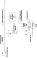
- FIG. 3A a schematic diagram illustrating various aspects of an antenna in an RFID system, for example the first antenna 210, is illustrated in accordance with various embodiments of the present disclosure.
- the first antenna 210 is part of an RFID system, for example the RFID system 100 with reference to FIG. 1 , or any other RFID system(s) used for identification, detection, tracking, etc.
- the RFID reading circuitry 202 is configured to provide an RF signal 320 of the first antenna over the coaxial cable 214 electronically coupled to the first antenna 210.
- the first antenna 210 includes an input connector 301 configured to electronically couple to the cable 214.
- the RFID reading circuitry 202 is configured to also provide a bias voltage of the first antenna over the coaxial cable 214 electronically coupled to the first antenna 210. In various embodiments, the bias voltage is used by various components of the antenna 210 to operate.
- the first antenna 210 includes a first attenuating coupler 322 of the first antenna configured to attenuate the RF signal 320 of the first antenna to generate a first attenuated RF signal 324 of the first antenna and a first step reduced RF signal 352 of the first antenna.
- the first attenuated RF signal 324 of the first antenna is used to determine a power level of the RF signal of the first antenna.
- using an attenuating coupler may allow for better conservation of the RF signal in the first antenna and in the chain of antennas as for example illustrated in FIG. 2 .
- the first step reduced RF signal 350 of the first antenna will not have much reduction in RF power compared to the RF signal 320 of the first antenna.
- an RF power detector 326 of the first antenna is configured to receive the first attenuated RF signal 324 of the first antenna and generate a power level indicator 328 of the RF signal of the first antenna.
- the power level indicator may be any value derived from the RF signal indicating the power level of the RF signal.
- the RF power detector 326 of the first antenna may determine a root mean square (RMS) value of the first attenuated RF signal 324 of the first antenna.
- the RF power detector 326 of the first antenna may determine the power level indicator 328 of the RF signal of the first antenna taking into account the attenuation provided by the first attenuating coupler 322 of the first antenna.
- the RF power detector 326 of the first antenna may scale up the detected RF power, proportional to the amount of the attenuation of the first attenuating coupler 322 of the first antenna, to determine the power level indicator 328 of the RF signal of the first antenna.
- the first antenna 210 includes an RF power comparator 330 of the first antenna.
- the RF power comparator 330 of the first antenna is configured to compare the power level indicator 328 of the RF signal of the first antenna with an RF signal power threshold.
- the RF signal power threshold is predetermined.
- the RF signal power threshold is dynamic and/or variable.
- the RF signal power threshold is selected to indicate the threshold below which the RF signal may not have enough power for communicating with one or more remote tags corresponding to the antenna.
- the RF power comparator 330 of the first antenna is configured to generate an RF power comparison output signal.
- the output of the RF power comparator 330 of the first antenna from the comparison of the power level indicator 328 of the RF signal of the first antenna and the RF signal power threshold generates a first input 332 to an Integrated Circuit (IC) tag 310 of the first antenna.
- the IC tag 310 of the first antenna performs various control and/or other functions in the first antenna as described herein.
- the antenna 210 includes a bias voltage comparator 334 of the first antenna.
- the bias voltage comparator 334 of the first antenna may be configured to compare the bias voltage of the first antenna with a bias voltage threshold.
- the bias voltage threshold is predetermined.
- the bias voltage threshold is dynamic and/or variable.
- the bias voltage threshold is selected to indicate the threshold below which the various components of the antenna may not receive enough power to function.
- the bias voltage is approximately 5 volts.
- the bias voltage threshold is between 3.5-4.5 volts.
- the bias voltage threshold is 4 volts.
- the bias voltage comparator 334 of the first antenna is configured to generate a voltage comparison output signal. In various embodiments, the output of the bias voltage comparator 334 of the first antenna generates a second input to the IC tag of the first antenna using the comparison of the bias voltage of the first antenna and the bias voltage threshold.
- the first antenna 210 includes a second attenuating coupler 338 of the first antenna.
- the second attenuating coupler 338 of the first antenna may be configured to attenuate the first step reduced RF signal 350 of the first antenna to generate a second attenuated RF signal 340 of the first antenna and a second step reduced RF signal 352 of the first antenna.
- using the second attenuating coupler 338 of the first antenna may allow for better conservation of the RF signal in the first antenna and in the chain of antennas as for example illustrated in FIG. 2 .
- the second step reduced RF signal 352 of the first antenna will not have much reduction in RF power compared to the first step reduced RF signal 35 of the first antenna.
- the first antenna 210 includes an RF fault bypass circuit 342 of the first antenna.
- the RF fault bypass circuit 342 when the bias voltage of the first antenna is greater than the bias voltage threshold, the RF fault bypass circuit 342 functions as an approximate open circuit. Accordingly, in various embodiments, when the bias voltage of the first antenna is above the bias voltage threshold, an output signal 344 of the RF fault bypass circuit of the first antenna is approximately zero.
- the RF fault bypass circuit 342 when the bias voltage of the first antenna is less than or equal to the bias voltage threshold, the RF fault bypass circuit 342 functions as an approximate short circuit. Accordingly, in various embodiments, when the bias voltage of the first antenna is less than or equal to the bias voltage threshold, the output signal 344 of the RF fault bypass circuit of the first antenna is approximately equal to the second step reduced RF signal 352 of the first antenna.
- the antenna 210 includes an RF power combiner 346 of the first antenna.
- the RF power combiner 346 is configured to combine the output signal 344 of the RF fault bypass circuit of the first antenna with the second attenuated RF signal 340 of the first antenna.
- an output of the power combiner 346 of the first antenna generates the RF input signal 312 to the IC tag 310 of the first antenna.
- the RF fault bypass circuit 342 of the first antenna is configured to increase a power of the RF input signal 312 to the IC tag 310 of the first antenna when a bias voltage of the first antenna falls below a bias voltage threshold.
- the output signal 344 of the RF fault bypass circuit of the first antenna is approximately zero. Therefore, in various embodiments, when the when the bias voltage of the first antenna is above the bias voltage threshold, the RF input signal 312 to the IC tag 310 of the first antenna is approximately equal to the second attenuated RF signal 340 of the first antenna.
- the RF input signal 312 to the IC tag 310 of the first antenna is approximately equal to the second attenuated RF signal 340 of the first antenna combined with the output signal 344 of the RF fault bypass circuit of the first antenna which under this condition is approximately equal to the second step reduced RF signal 352 of the first antenna.
- the power of the RF input signal 312 to the IC tag 310 of the first antenna is increased.
- the first antenna 210 includes the IC tag 310 of the first antenna.
- the IC tag 310 of the first antenna may be configured to provide control and/or diagnosis function(s) in the first antenna 210.
- the IC tag 310 may control an RF switch 302 of the first antenna.
- the IC tag 310 provides diagnosis information to the RFID reading circuitry 202 with respect any of the RF signal and/or bias voltage failure(s) to the RFID reading circuitry 202 as for example described below.
- the first antenna 210 includes a radio frequency (RF) switch 302 of the first antenna.
- the RF switch 302 of the first antenna may be configured to receive a switch RF signal 304 of the first antenna.
- the RF switch 302 of the first antenna may switch the switch RF signal 304 of the first antenna to a radiating element 306 of the first antenna or to an output 308 of the first antenna.
- the IC tag 310 may be configured to control whether the RF switch 302 of the first antenna switches the switch RF signal 304 of the first antenna to the output 308 of the first antenna or to the radiating element 306 of the first antenna.
- the RF fault bypass circuit 342 when the bias voltage of the first antenna 210 is above the bias voltage threshold, the RF fault bypass circuit 342 functions as an approximate open circuit and the switch RF signal 304 of the first antenna is approximately equal to the second step reduced RF signal 352 of the first antenna. Therefore, under a normal operating condition with respect to the bias voltage, when the first antenna 210 receives proper bias voltage (above the bias voltage threshold), the RF switch 302 of the first antenna receives most of the RF signal 320 of the first antenna (expect for the relatively small reductions in the RF signal power caused by the first and second attenuating couplers of the first antenna).
- the RF switch 302 of the first antenna switches most of the RF signal 320 of the first antenna to the output 308 of the first antenna or to the radiating element 306 of the first antenna.
- the second antenna 212 is electronically coupled to the output 308 of the first antenna such that when RF switch 302 of the first antenna switches most of the RF signal 320 of the first antenna to the output 308, it is received by the second antenna 212 in the first chain of antennas 204.
- the RF switch 302 of the first antenna switches most of the RF signal 320 of the first antenna to the radiating element 306 of the first antenna to be radiated to a field of view of the first antenna 210, or the RF switch 302 of the first antenna switches most of the RF signal 320 of the first antenna to the output 308 of the first antenna which is coupled to the input of the second antenna 212.
- the IC tag 310 of the first antenna controls the switching function of the RF switch 302 of the first antenna.
- the RFID reading circuitry 202 may direct the IC tag 310 of the first antenna to control the RF switch 302 of the first antenna to switch the switch RF signal 304 of the first antenna to the radiating element 306 of the first antenna.
- the RFID reading circuitry 202 may direct the IC tag 310 of the first antenna to control the RF switch 302 of the first antenna to switch the switch RF signal 304 of the first antenna to the second antenna 212 via the output 308 of the first antenna.
- the RFID system 100 includes one or more remote tags.
- each antenna of the one or more antennas of the RFID system 100 may correspond to one or more remote tags.
- the first antenna 210 may correspond with one or more remote tags.
- each remote tag corresponding to the first antenna 210 is configured to, when the RF switch 302 of the first antenna switches the switch RF signal of the first antenna to the radiating element of the first antenna, receive a radiation from the radiating element of the first antenna and emit a return radiation to the radiating element of the first antenna.
- the first remote tag 371 and the second remote tag 372 may correspond to the first antenna 210.
- the first remote tag 371 and the second remote tag 372 receive a radiation 370 from the radiating element 306 of the first antenna.
- the first remote tag 371 may emit a return radiation 373 corresponding to the first remote tag and the second remote tag 372 may emit a return radiation 374 corresponding to the second remote tag to the radiating element 306.
- the antenna 210 identifies, determines a presence of, or otherwise detects any remote tag(s) corresponding to the first antenna.
- each of the tag(s) may be attached to, placed in, or otherwise uniquely associated with an object in a field of view of the radiating element of the antenna.
- the antenna may identify, determine a presence of, or otherwise detect any object(s) in its field of view.
- the RFID reading circuitry 202 is configured to identify and/or detect each of the one or more remote tags corresponding to the first antenna 210 and/or indicate a presence of each of the one or more remote tags corresponding to the first antenna, using the return radiation from the corresponding each of the one or more remote tags corresponding to the first antenna.
- each of the remote tags may be attached to, located in, or otherwise associated with an object, hence identifying, indicating a presence of, and/or detecting each tag may correspond to that of the associated object.
- FIG. 3B a schematic diagram illustrating various aspects of an antenna in an RFID system, for example the first antenna 210, is illustrated in accordance with various embodiments of the present disclosure.
- the RFID reading circuitry 202 is electronically coupled to the input port 301 to provide the RF signal 320 of the first antenna and the bias voltage 404 of the first antenna.
- the first antenna 210 includes a first RF choke circuitry 380.
- the first RF choke circuitry 380 is configured to separate the RF signal 320 of the first antenna from the bias voltage 404 of the first antenna.
- the bias voltage 404 of the first antenna is provided to various components of the first antenna 210 that require a bias voltage to operate, such as the RF power comparator 330 of the first antenna, the RF power detector 326 of the first antenna, the IC tag 310 of the first antenna, the bias voltage comparator 334 of the first antenna, the RF switch 302 of the first antenna, an RF signal loss visual indicator 552, and a bias voltage loss visual indicator 554 (as described below), etc.
- the first RF choke circuitry 380 prevents the RF signal from reaching the bias voltage input of various components of the antenna 210 and prevents the bias voltage from reaching RF inputs of various components such as the first attenuating coupler 322 of the first antenna, the second attenuating coupler 338 of the first antenna, the RF fault bypass circuit 342 of the first antenna, the RF switch 302 of the first antenna etc.
- the first RF choke circuitry may be a signal splitter.
- the first antenna 210 includes a second RF choke circuitry 382.
- the second RF choke circuitry 382 is configured to add the bias voltage back on a main RF cable of the first antenna such that a combination of both bias voltage and an RF signal is provided to the second antenna.
- the second RF choke circuitry 382 adds the bias voltage 404 of the first antenna to the switch RF signal 304 of the first antenna and a combination of the bias voltage and the RF signal is provided to the output 308 of the first antenna and to an input of the second antenna.
- the second RF choke circuitry may be a signal combiner.
- FIG. 4 a schematic diagram illustrating various aspects of some of the components of the first antenna is provided in accordance with various embodiments of the present disclosure.
- the IC tag 310 of the first antenna when the bias voltage 404 of the first antenna 210 is above the bias voltage threshold, the IC tag 310 of the first antenna operates in a semi-passive mode and emits a first return radiation 402 from the IC tag of the first antenna with a low power.
- the semi-passive mode is the normal operation mode for the IC tag 310 of the first antenna. In the semi-passive mode, the IC tag 310 of the first antenna has high sensitivity and can function with a low power of the RF input signal 312 to the IC tag 310 of the first antenna.
- the output signal 344 of the RF fault bypass circuit of the first antenna is approximately zero. Therefore, under the normal operating condition of the first antenna 210 with respect to the bias voltage, the IC tag 310 of the first antenna receives a low power input approximately equal to the second attenuated RF signal 340 of the first antenna. Therefore, in various embodiments, the first return radiation from the IC tag of the first antenna is relatively low under such conditions.
- the RFID reading circuitry 202 is configured to detect the first return radiation from the IC tag of the first antenna after it passes through the second attenuating coupler 338 again (and may be further attenuated) and is transmitted over the coaxial cable to the RFID reading circuitry 202.
- the IC tag 310 of the first antenna when the bias voltage 404 of the first antenna 210 is below or equal to the bias voltage threshold, the IC tag 310 of the first antenna operates in a passive mode and emits a second return radiation 403 from the IC tag of the first antenna with a high power.
- the power level of the second return radiation 403 from the IC tag of the first antenna is greater than the power level of the first return radiation 402 from the IC tag of the first antenna.
- the IC tag 310 of the first antenna In the passive mode, the IC tag 310 of the first antenna has low sensitivity and requires a high power of the RF input signal 312 to the IC tag 310 of the first antenna to operate.
- the output signal 344 of the RF fault bypass circuit of the first antenna is approximately equal to the second step reduced RF signal 352 of the first antenna. Therefore, under a fault condition of the first antenna 210 with respect to the bias voltage, the IC tag 310 of the first antenna receives a high-power input close to the power of the RF signal 320 of the first antenna. Therefore, in various embodiments, the first return radiation from the IC tag of the first antenna is relatively high under such conditions.
- the RFID reading circuitry 202 is configured to detect the first return radiation from the IC tag of the first antenna after a portion of it passes through the second attenuating coupler 338 again (and may be further attenuated) and a portion of it passes through the RF fault bypass circuit 342 (approximately without any attenuation) and is transmitted over the coaxial cable to the RFID reading circuitry 202.
- the RFID reading circuitry 202 is configured to determine whether a fault in the RFID system exists using any of the bias voltage of the first antenna, a power level indicator of the RF signal of the first antenna, and the increase in the power of the RF input signal to the IC tag of the first antenna. In various embodiments, the RFID circuitry 202 determines the increase in the power of the RF input signal to the IC tag of the first antenna using the received first return radiation 402 or second return radiation 403 from the IC tag of the first antenna.
- the RFID reading circuitry 202 may determine a change in the bias voltage of the first antenna or the power level indicator of the RF signal of the first antenna by querying the IC tag 310 and/or determining the values of the first input 332 or the second input 336 to the IC tag of the first antenna.
- a power of the first step reduced RF signal 350 may be approximately 20dBm
- a power of the second attenuated RF signal 340 may be approximately -15dBm (assuming the second attenuating coupler 338 of the first antenna is a 35dBm coupler)
- the power of the first return radiation 402 in a semi-passive mode of the IC tag may be approximately -25dBm
- the power of the second return radiation 403 in the passive mode of the IC tag may be approximately 10dBm.
- the values may be lower for the other antennas due to signal loss in cables and/or RF switches.
- the signal powers may be reduced by about 2dBm. It is noted however, that these values are for example and illustration purposes and the signals may be any other power values in accordance with various embodiments of the present disclosure.
- the first antenna 210 is electronically coupled to an RF signal loss visual indicator 552 of the first antenna.
- the first antenna 210 is electronically coupled to a bias voltage loss visual indicator 554 of the first antenna.
- the RF signal loss visual indicator 552 of the first antenna includes a light emitting diode (LED).
- bias voltage loss visual indicator 554 of the first antenna includes a light emitting diode (LED).
- the RF signal loss visual indicator 552 of the first antenna is electronically coupled to the first input 332 to the IC tag of the first antenna. In various embodiments, the RF signal loss visual indicator 552 of the first antenna receive the first input to the IC tag of the first antenna and visually indicates whether the power level indicator of the RF signal of the first antenna is less than the RF signal power threshold.
- the bias voltage loss visual indicator 554 of the first antenna is electronically coupled to the second input 336 to the IC tag of the first antenna. In various embodiments, the bias voltage loss visual indicator 554 of the first antenna receive the second input to the IC tag of the first antenna and visually indicate whether the bias voltage of the first antenna is less than the bias voltage threshold.
- loss of RF signal or bias voltage may be visually displayed at or in proximity of each antenna. Additionally and/or alternatively, the status of the RF signal and bias voltage of the first antenna may be communicated back to the RFID reading circuitry 202.
- the RFID reading circuitry determines the status of the RF signal and bias voltage of the first antenna by querying the IC tag 310 of the first antenna and reading the values of the first and second inputs to the IC tag of the first antenna.
- the RFID system 100 may include a dashboard including one or more visual indicators and/or a display for displaying the status of the RF signal and bias voltage for any of the antennas of the RFID system 100.
- the second antenna 212 is electronically coupled to the output 308 of the first antenna 210.
- a coaxial cable input of the second antenna 210 is electronically coupled to the output 308 of the first antenna.
- the second antenna 212 may include components and/or perform functions similar to those of antenna 210 as described above.
- the second antenna 212 includes an RF switch of the second antenna.
- the RF switch of the second antenna is configured to receive a switch RF signal of the second antenna, and switch the switch RF signal of the second antenna to a radiating element of the second antenna or to an output of the second antenna.
- the second antenna includes an IC tag of the second antenna.
- the IC tag of the second antenna is configured to control the RF switch of the second antenna.
- the second antenna includes an RF fault bypass circuit of the second antenna.
- the RF fault bypass circuit of the second antenna is configured to increase a power of an RF input signal to the IC tag of the second antenna when a bias voltage of the second antenna falls below the bias voltage threshold.
- the second antenna is configured to receive an RF signal of the second antenna from the output of the first antenna when the RF switch of the first antenna switches the switch RF signal of the first antenna to the output of the first antenna.
- the second antenna is configured to receive the bias voltage of the second antenna from the output of the first antenna.
- the RF signal of the second antenna and the bias voltage of the second antenna is transmitted to the second antenna via the coaxial cable 216.
- the second antenna is configured to receive the RF signal of the second antenna and the bias voltage of the second antenna using a coaxial cable input to the second antenna.
- the RFID system 100 includes one or more remote tags corresponding to the second antenna each configured to, when the RF switch of the second antenna switches the switch RF signal of the second antenna to the radiating element of the second antenna, receive a radiation from the radiating element of the second antenna and emit a return radiation to the radiating element of the second antenna.
- the RFID reading circuitry 202 is configured to identify each of the one or more remote tags corresponding to the second antenna or indicate a presence of the one or more remote tags corresponding to the second antenna, using the return radiation from the corresponding each of the one or more remote tags corresponding to the second antenna.
- the second antenna 212 includes a first attenuating coupler of the second antenna configured to attenuate the RF signal of the second antenna to generate a first attenuated RF signal of the second antenna and a first step reduced RF signal of the second antenna.
- the second antenna 212 includes an RF power detector of the second antenna configured to receive the first attenuated RF signal of the second antenna and generate a power level indicator of the RF signal of the second antenna.
- the second antenna 212 includes an RF power comparator of the second antenna.
- the RF power comparator of the second antenna is configured to compare the power level indicator of the RF signal of the second antenna with the RF signal power threshold and generate a first input to the IC tag of the second antenna using the comparison of the power level indicator of the RF signal of the second antenna and the RF signal power threshold.
- the second antenna 212 includes an RF signal loss visual indicator of the second antenna.
- the RF signal loss visual indicator of the second antenna may be an LED.
- the RF signal loss visual indicator of the second antenna is configured to receive the first input to the IC tag of the second antenna, and visually indicate whether the power level indicator of the RF signal of the second antenna is less than the RF signal power threshold.
- the LED used as the RF signal loss visual indicator of the second antenna turns on when the power level indicator of the RF signal of the second antenna is less than the RF signal power threshold, or vice versa.
- the second antenna 212 includes a bias voltage comparator of the second antenna.
- the bias voltage comparator of the second antenna is configured to compare the bias voltage of the second antenna with the bias voltage threshold.
- the bias voltage comparator of the second antenna is configured to generate a second input to the IC tag of the second antenna using the comparison of the bias voltage of the second antenna and the bias voltage threshold.
- the second antenna 212 includes a bias voltage loss visual indicator of the second antenna.
- the bias voltage visual indicator of the second antenna may be an LED.
- the bias voltage visual indicator of the second antenna is configured to receive the second input to the IC tag of the second antenna and visually indicate whether the bias voltage of the second antenna is less than the bias voltage threshold.
- the LED used as the bias voltage loss visual indicator of the second antenna turns on when the bias voltage indicator of the bias voltage of the second antenna is less than the bias voltage threshold, or vice versa.
- the second antenna 212 includes a second attenuating coupler of the second antenna.
- the second attenuating coupler of the second antenna is configured to attenuate the first step reduced RF signal of the second antenna to generate a second attenuated RF signal of the second antenna at an output of the second attenuating coupler of the second antenna, and a second step reduced RF signal of the second antenna, for example on a coaxial cable of the first antenna.
- the second antenna 212 includes an RF power combiner of the second antenna.
- the RF power combiner of the second antenna is configured to combine an output signal of the RF fault bypass circuit of the second antenna with the second attenuated RF signal of the second antenna to generate an RF input signal to the IC tag of the second antenna.
- the output signal of the RF fault bypass circuit of the second antenna is approximately zero and the switch RF signal of the second antenna is approximately equal to the second step reduced RF signal of the second antenna.
- the IC tag of the second antenna when the bias voltage of the second antenna is above the bias voltage threshold, the IC tag of the second antenna operates in a semi-passive mode and emits a first return radiation from the IC tag of the second antenna. In various embodiments, the IC tag of the second antenna is configured to operate in a semi-passive mode when the bias voltage provided to it is above the bias voltage threshold.
- the RFID reading circuitry 202 detects the first return radiation from the IC tag of the second antenna and determines a power level of it. In various embodiments, the power level of the first return radiation from the IC tag of the second antenna is less than a power level of a second return radiation from the IC tag of the second antenna when the IC tag of the second antenna operates in a passive mode.
- the output signal of the RF fault bypass circuit of the second antenna is approximately equal to the second step reduced RF signal of the second antenna.
- the IC tag of the second antenna is configured to operate in the passive mode. Therefore, in various embodiments, when the bias voltage of the second antenna falls below the bias voltage threshold and the IC tag of the second antenna operates in the passive mode, it emits a second return radiation from the IC tag of the second antenna. In various embodiments, a power level of the second return radiation from the IC tag of the second antenna is greater than a power level of the first return radiation from the IC tag of the second antenna. In various embodiments, the RFID reading circuitry received the first and second return radiations from the IC tag of the second antenna and determines the corresponding power levels.
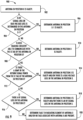
- step 602 if the RFID reading circuitry 202 does not receive the return radiation in response to the radiation from the radiating element of the second antenna or when the RFID reading circuitry 202 does not receive the first return radiation from the IC tag of the second antenna, the RFID reading circuitry 202 determines that the second antenna position is faulty and/or a fault exists in the RFID system 100.
- the RFID reading circuitry 202 determines that the fault in the RFID system includes and/or is an RF signal failure in the first antenna if the power level indicator of the RF signal of the first antenna is less than the RF signal power threshold. In various embodiments, the RFID reading circuitry 202 determines that the RF signal of the first antenna is less than the RF signal power threshold using the first input 332 to the IC tag of the first antenna. In various embodiments, the RFID reading circuitry 202 may determine the first input to the IC tag of the first antenna by querying the IC tag 310 of the first antenna. In various embodiments, the RF signal loss visual indicator of the first antenna may be additionally and/or instead be checked for determining that the RF signal of the first antenna is less than the RF signal power threshold.
- the RFID reading circuitry 202 determines that the fault in the RFID system includes and/or is a bias voltage failure in the first antenna if the bias voltage of the first antenna is less than the bias voltage threshold. In various embodiments, the RFID reading circuitry 202 determines that the bias voltage of the first antenna is less than the bias voltage threshold using the second input 336 to the IC tag of the first antenna. In various embodiments, the RFID reading circuitry 202 may determine the second input to the IC tag of the first antenna by querying the IC tag 310 of the first antenna. In various embodiments, the bias voltage loss visual indicator of the first antenna may be additionally and/or instead be checked for determining that the bias voltage of the first antenna is less than the bias voltage threshold.
- the RFID reading circuitry 202 determines whether it can communicate with the IC tag of the second antenna.
- the RFID reading circuitry determines that the fault in the RFID system includes and/or is any of a fault in a connection between the first and second antenna (for example the cable 216 and/or a connection between the output 308 of the first antenna and the cable 216) and/or a fault in the RF switch of the first antenna.
- the RF switch of the first antenna may not be switching the switch RF signal 304 of the first antenna to the output 308 of the first antenna.
- the output 308 of the first antenna may be faulty and/or not be receiving an output from the RF signal 304 of the first antenna.
- the RFID reading circuitry determines whether it receives the second return radiation from the IC tag of the second antenna.
- the second return radiation from the IC tag of the second antenna has a higher power value than the first return radiation from the IC tag of the second antenna.
- the second return radiation from the IC tag of the second antenna has about 5-15dB, for example about 10dB, higher power value than the first return radiation from the IC tag of the second antenna.
- the RFID reading circuitry determines whether it receives the second return radiation from the IC tag of the second antenna by determining whether there is a jump in the power of the return radiation from the IC tag of the second antenna, for example by about 5-15dB, for example by about 10dB.
- the RFID reading circuitry determines that the fault in the RFID system comprises a bias voltage failure in the second antenna when the RFID reading circuitry receives the second return radiation from the IC tag of the second antenna.
- the RFID reading circuitry when the RFID reading circuitry receives the first return radiation from the IC tag of the second antenna, if the power level indicator of the RF signal of the second antenna is less than the RF signal power threshold, at step 610, the RFID reading circuitry is configured to determine the fault in the RFID system includes and/or is an RF signal failure in the second antenna. In various embodiments, the RFID reading circuitry determines whether the power level indicator of the RF signal of the second antenna is less than the RF signal power threshold, using the first input to the IC tag of the second antenna.
- the RFID reading circuitry when the RFID reading circuitry receives the first return radiation from the IC tag of the second antenna, if the power level indicator of the RF signal of the second antenna is equal to or greater than the RF signal power threshold, at step 612, the RFID reading circuitry determines that the fault in the RFID system includes and/or is a fault in the radiating element of the second antenna, if the power level indicator of the RF signal of the second antenna is equal to or greater than the RF signal power threshold, using the first input to the IC tag of the second antenna.
- the RF fault bypass circuit 342 includes an electromechanical switch 702.
- the electromechanical switch when the bias voltage 404 is equal to or above the bias voltage threshold, the electromechanical switch is configured to provide a switching function such that the second step reduced RF signal provided to an input 701 of the RF fault bypass circuit faces an approximate open circuit.
- the electromechanical switch when the bias voltage 404 is equal to or above the bias voltage threshold, switches the input 701 to a quarter wavelength impedance transformer 703 electronically coupled to a capacitance circuitry 704.
- the capacitance circuitry 704 includes a capacitor with a capacitance in the range of 10-200 pf, 50-150 pf, or for example with a capacitance of approximately 100 pf.
- the quarter wavelength impedance transformer 703 transforms the impedance of the capacitor 704 so the RF signal on the input 701 faces an approximate open circuit.
- the RF fault bypass circuit 342 includes the electromechanical switch 702.
- the electromechanical switch when the bias voltage 404 is below the bias voltage threshold, the electromechanical switch switches the input 701 to an output of the RF fault bypass circuit 342 which is electronically coupled to the RF power combiner 346. Therefore, in various embodiments, when the bias voltage 404 is below the bias voltage threshold, the electromechanical switch is configured to provide a switching function such that the second step reduced RF signal provided to an input 701 of the RF fault bypass circuit faces an approximate short circuit to the output of the RF fault bypass circuit 342 coupled to the power combiner 346. In various embodiments, the second attenuating coupler 338 is bypassed by the RF fault bypass circuit 342 when the bias voltage 404 is below the bias voltage threshold.
- the RFID system 100 includes a plurality of antennas, for example including first antenna 210 and second antenna 212.
- the first antenna 210 and the second antenna 212 may be placed in any locations in the chain of antennas 204.
- each antenna of the plurality of antennas includes an RF power comparator (for example including or similar to the RF power comparator 330 of the first antenna), a bias voltage comparator (for example including or similar to the bias voltage comparator 334 of the first antenna), and an RF fault bypass circuit (for example including or similar to the RF fault bypass circuit 342 of the first antenna).
- the RF power comparator of each antenna is configured to compare the power level indicator of the RF signal of the antenna with an RF signal power threshold.
- the bias voltage comparator is configured to compare a bias voltage of the antenna with a bias voltage threshold.
- the RF fault bypass circuit configured to function as an approximate open circuit when the bias voltage of the antenna is equal to or higher than the bias voltage threshold and function as an approximate short circuit when the bias voltage of the antenna is lower than the bias voltage threshold.
- the RFID system 100 includes an RFID reading circuitry 202.
- the RFID reading circuitry 202 is configured to determine a fault in the RFID system using any of the RF power comparison, bias voltage comparison, and function of the RF fault bypass circuit as for example using the method 600 described with reference to FIG. 6 .
- FIG. 8 a flowchart illustrating a method 800 is provided in accordance with various embodiments of the present disclosure.
- the method 800 may be performed by one or more components of an RFID system.
- the RFID system may be similar to the RFID system 100 described above.
- the RFID system may include a controller 1000 as described below with reference FIG. 10 .
- the memory of the controller of the RFID system may store computer program instructions implementing the method 800.
- various components of the RFID system 100 for example the RFID reading circuitry 202, include the controller and/or are implemented using the controller.
- a controller determines a failure by an antenna of an antenna chain of the RFID system 100 in detecting a remote tag associated with the antenna.
- the controller determines a prior antenna in the antenna chain as faulty if an RF signal loss or a bias voltage loss is occurred in the prior antenna. In various embodiments, at step 806, the controller determines the antenna is faulty if there are no RF signal loss or bias voltage loss in the prior antenna, and if an RFID reading circuitry is not able to communicate with an integrated circuit (IC) tag of the antenna or the RFID reading circuitry detects a jump in a return signal power from the IC tag of the antenna.
- IC integrated circuit
- the controller determines, determines, when the RFID reading circuitry communicates with the IC tag of the antenna and the RFID reading circuitry does not detect the jump in the return signal power from the IC tag of the antenna, the antenna is faulty if an RF signal loss or a bias voltage loss is occurred in the antenna.
- the method 900 may be performed by one or more components an RFID system.
- the RFID system may be similar to the RFID system 100 described above.
- the RFID system may include a controller 1000 as described below with reference FIG. 10 .
- the memory of the controller of the RFID system may store computer program instructions for implementing the method 900.
- various components of the RFID system 100 for example the RFID reading circuitry 202, include the controller and/or are implemented using the controller.
- a controller determines that an antenna in a position X of an antenna chain is faulty.
- a faulty antenna may be determined when no remote tags associated to the antenna are detected.
- a faulty antenna may be detected when the RFID reader cannot query and/or communicate with the IC tag of the antenna.
- the controller determines whether an RF signal loss or a bias voltage loss is determined in the antenna in position X-1. If so, at step 906, the controller determined that the antenna in position X-1 and/or antennas in position X-1 onwards are faulty. In various embodiments, the controller determines and/or generates an output indicating whether the RF signal or the bias voltage loss has occurred in antenna in position X-1. In various embodiments, visual indicators indicating RF signal and/or bias voltage loss on the antenna in position X-1 may be used to determine and locate the RF signal and/or bias voltage loss. In various embodiments, the controller repeats the above steps for antennas in position X-2, etc.
- the controller determines whether it can communicate with the IC tag of the antenna in position X.
- the RFID reading circuitry 202 determines whether it can communicate with the IC tag of the antenna in position X.
- the controller determines that the antenna in position X, and/or the antenna in position X and onwards are faulty. In various embodiments, the controller determines at step 910, that an RF cable between antennas in positions X an X-1 is faulty, an RF switch of antenna X-1 is faulty, or an output of antenna X-1 is faulty. In various embodiments, at step 910, the controller determines that either both the RF signal and the bias voltage are lost in antenna in position X, or only the RF signal is lost in antenna in position X.
- the controller may determine that the RF switch of antenna in position X-1 is faulty, hence no RF signal is reaching the antenna in position X.
- the controller may use first and second inputs to the IC tag of the antenna in position X to determine whether the RF signal and/or the bias voltage of the antenna in position X are lost.
- the controller determines whether there is an RF loss in the antenna in position X. In various embodiments, the controller determines whether there is an RF loss in the antenna in position X using the first input to the IC tag of the antenna in position X. The controller may determine the first input to the IC tag of the antenna in position X by querying the IC tag of the antenna in position X.
- the controller determines an RF signal loss in the antenna of position X
- the controller at step 918 determines that the antenna in position X is faulty and/or the antenna in position X and following antennas are faulty.
- the RF signal loss visual indicators on the antenna in position X and the following antennas may be used to determine which antenna is faulty.
- the controller determines that there is no RF signal loss in the antenna of position X, the controller at step 920 determines that there is a fault with the radiating element of the antenna of position X and/or there are no remote tags associated with antenna X are present.
- the controller 1000 may be in electronic communications with any of the components of the RFID system 100 and/or any of the components of the RFID system 100 may include a controller.
- the controller 1000 comprises processing circuitry 502, a communication module 508, input/output module 506, a memory 504 and/or other components configured to perform various operations, procedures, functions or the like described herein.
- the controller 1000 (such as the processing circuitry 502, communication module 508, input/output module 506 and memory 504) is electrically coupled to and/or in electronic communication with various components of the RFID system.
- the RFID reading circuitry 202 may include the controller 1000 and/or the processing circuitry 502.
- the processing circuitry 502 may be implemented as, for example, various devices comprising one or a plurality of microprocessors with accompanying digital signal processors; one or a plurality of processors without accompanying digital signal processors; one or a plurality of coprocessors; one or a plurality of multi-core processors; one or a plurality of controllers; processing circuits; one or a plurality of computers; and various other processing elements (including integrated circuits, such as ASICs or FPGAs, or a certain combination thereof).
- the processing circuitry 502 may comprise one or more processors.
- the processing circuitry 502 is configured to execute instructions stored in the memory 504 or otherwise accessible by the processing circuitry 502.
- these instructions may enable the controller 1000 to execute one or a plurality of the functions as described herein.
- the processing circuitry 502 may comprise entities capable of executing operations according to the embodiments of the present invention when correspondingly configured. Therefore, for example, when the processing circuitry 502 is implemented as an ASIC, an FPGA, or the like, the processing circuitry 502 may comprise specially configured hardware for implementing one or a plurality of operations described herein.
- the instructions may specifically configure the processing circuitry 502 to execute one or a plurality of methods, algorithms and operations described herein, such as those discussed with reference to any of the flowcharts herein.
- the memory 504 may comprise, for example, a volatile memory, a non-volatile memory, or a certain combination thereof. Although illustrated as a single memory in FIG. 5 , the memory 504 may comprise a plurality of memory components. In various embodiments, the memory 504 may comprise, for example, a hard disk drive, a random access memory, a cache memory, a flash memory, a Compact Disc Read-Only Memory (CD-ROM), a Digital Versatile Disk Read-Only Memory (DVD-ROM), an optical disk, a circuit configured to store information, or a certain combination thereof. The memory 504 may be configured to store information, data, application programs, instructions, and etc., so that the controller 1000 can execute various functions according to the embodiments of the present disclosure.
- the memory 504 is configured to cache input data for processing by the processing circuitry 502. Additionally or alternatively, in at least some embodiments, the memory 504 is configured to store program instructions for execution by the processing circuitry 502.
- the memory 504 may store information in the form of static and/or dynamic information. When the functions are executed, the stored information may be stored and/or used by the controller 1000.
- the communication module 508 may be implemented as any apparatus included in a circuit, hardware, a computer program product or a combination thereof, which is configured to receive and/or transmit data from/to another component or apparatus.
- the computer program product comprises computer-readable program instructions stored on a computer-readable medium (for example, the memory 504) and executed by a controller 1000 (for example, the processing circuitry 502).
- the communication module 508 (as with other components discussed herein) may be at least partially implemented as the processing circuitry 502 or otherwise controlled by the processing circuitry 502.
- the communication module 508 may communicate with the processing circuitry 502, for example, through a bus.
- the communication module 508 may comprise, for example, antennas, transmitters, receivers, transceivers, network interface cards and/or supporting hardware and/or firmware/software, and is used for establishing communication with another apparatus.
- the communication module 508 may be configured to receive and/or transmit any data that may be stored by the memory 504 by using any protocol that can be used for communication between apparatuses.
- the communication module 508 may additionally or alternatively communicate with the memory 504, the input/output module 506 and/or any other component of the controller 1000, for example, through a bus.
- the controller 1000 may comprise an input/output module 506.
- the input/output module 506 may communicate with the processing circuitry 502 to receive instructions input by the user and/or to provide audible, visual, mechanical or other outputs to the user. Therefore, the input/output module 506 may be in electronic communication with supporting devices, such as a keyboard, a mouse, a display, a touch screen display, and/or other input/output mechanisms. Alternatively, at least some aspects of the input/output module 506 may be implemented on a device used by the user to communicate with the controller 1000.
- the input/output module 506 may communicate with the memory 504, the communication module 508 and/or any other component, for example, through a bus.
- One or a plurality of input/output modules and/or other components may be included in the controller 1000.
- one or more of the procedures and/or methods described herein, for example in FIG. 6 , 8 , 9 may be embodied by computer program instructions, which may be stored by a memory (such as a non-transitory memory) of a system employing an embodiment of the present disclosure and executed by a processing circuitry (such as a processor) of the system.
- These computer program instructions may direct the system to function in a particular manner, such that the instructions stored in the memory circuitry produce an article of manufacture, the execution of which implements the function specified in the flow diagram step/operation(s).
- the system may comprise one or more other circuitries.
- Various circuitries of the system may be electronically coupled between and/or among each other to transmit and/or receive energy, data and/or information.
- embodiments may take the form of a computer program product on a non-transitory computer-readable storage medium storing computer-readable program instruction (e.g., computer software). Any suitable computer-readable storage medium may be utilized, including non-transitory hard disks, CD-ROMs, flash memory, optical storage devices, or magnetic storage devices.
Landscapes
- Engineering & Computer Science (AREA)
- Physics & Mathematics (AREA)
- General Physics & Mathematics (AREA)
- Theoretical Computer Science (AREA)
- Health & Medical Sciences (AREA)
- Artificial Intelligence (AREA)
- Computer Vision & Pattern Recognition (AREA)
- Computer Networks & Wireless Communication (AREA)
- Electromagnetism (AREA)
- Toxicology (AREA)
- General Health & Medical Sciences (AREA)
- Signal Processing (AREA)
- Microelectronics & Electronic Packaging (AREA)
- Computer Hardware Design (AREA)
- Biomedical Technology (AREA)
- Near-Field Transmission Systems (AREA)
Abstract
Description
- Radio frequency identification (RFID) system may be used to account for and/or track various objects such as items in an inventory and/or in a warehouse, parts in an assembly line, boxes on a delivery truck, etc. Various antennas may be used to send and/or receive radio frequency signals used for detection. In some instances, however, a component of the RFID system or a component of one of the antennas may fail.
- Applicant has identified many technical challenges and difficulties associated with RFID systems. Through applied effort, ingenuity, and innovation, Applicant has solved problems related to identifying and/or gaining more information about a failure in the system by developing solutions embodied in the present disclosure, which are described in detail below.
- Various embodiments described herein relate to methods, apparatuses, and systems for fault diagnosis in an RFID system.
- Various embodiments of the present disclosure provide a frequency identification (RFID) system comprising a first antenna comprising a radio frequency (RF) switch of the first antenna configured to receive a switch RF signal of the first antenna; and switch the switch RF signal of the first antenna to a radiating element of the first antenna or to an output of the first antenna; an integrated circuit (IC) tag of the first antenna configured to control the RF switch of the first antenna; and an RF fault bypass circuit of the first antenna configured to increase a power of an RF input signal to the IC tag of the first antenna when a bias voltage of the first antenna falls below a bias voltage threshold; and an RFID reading circuitry configured to: provide an RF signal of the first antenna and the bias voltage of the first antenna; and determines whether a fault in the RFID system exists using any of the bias voltage of the first antenna, a power level indicator of the RF signal of the first antenna, and the increase in the power of the RF input signal to the IC tag of the first antenna.
- In various embodiments, the RFID system comprising one or more remote tags corresponding to the first antenna each configured to, when the RF switch of the first antenna switches the switch RF signal of the first antenna to the radiating element of the first antenna: receive a radiation from the radiating element of the first antenna; and emit a return radiation to the radiating element of the first antenna, wherein the RFID reading circuitry is configured to identify each of the one or more remote tags corresponding to the first antenna or indicate a presence of each of the one or more remote tags corresponding to the first antenna, using the return radiation from the corresponding each of the one or more remote tags corresponding to the first antenna.
- In various embodiments, the RFID system comprising: a first attenuating coupler of the first antenna configured to attenuate the RF signal of the first antenna to generate a first attenuated RF signal of the first antenna and a first step reduced RF signal of the first antenna; an RF power detector of the first antenna configured to receive the first attenuated RF signal of the first antenna and generate the power level indicator of the RF signal of the first antenna; an RF power comparator of the first antenna configured to: compare the power level indicator of the RF signal of the first antenna with an RF signal power threshold; and generate a first input to the IC tag of the first antenna using the comparison of the power level indicator of the RF signal of the first antenna and the RF signal power threshold; and an RF signal loss visual indicator of the first antenna configured to: receive the first input to the IC tag of the first antenna; and visually indicate whether the power level indicator of the RF signal of the first antenna is less than the RF signal power threshold.
- In various embodiments, the RFID system comprising: a bias voltage comparator of the first antenna configured to: compare the bias voltage of the first antenna with the bias voltage threshold; generate a second input to the IC tag of the first antenna using the comparison of the bias voltage of the first antenna and the bias voltage threshold; and a bias voltage loss visual indicator of the first antenna configured to: receive the second input to the IC tag of the first antenna; and visually indicate whether the bias voltage of the first antenna is less than the bias voltage threshold.
- In various embodiments, the RFID system comprising: a second attenuating coupler of the first antenna configured to attenuate the first step reduced RF signal of the first antenna to generate a second attenuated RF signal of the first antenna and a second step reduced RF signal of the first antenna; and an RF power combiner of the first antenna configured to combine an output signal of the RF fault bypass circuit of the first antenna with the second attenuated RF signal of the first antenna.
- In various embodiments, the bias voltage of the first antenna is above the bias voltage threshold: the switch RF signal of the first antenna is approximately equal to the second step reduced RF signal of the first antenna; the output signal of the RF fault bypass circuit of the first antenna is approximately zero; and the IC tag of the first antenna operates in a semi-passive mode and emits a first return radiation from the IC tag of the first antenna.
- In various embodiments, the bias voltage of the first antenna falls below the bias voltage threshold: the output signal of the RF fault bypass circuit of the first antenna is approximately equal to the second step reduced RF signal of the first antenna; and the IC tag of the first antenna operates in a passive mode and emits a second return radiation from the IC tag of the first antenna, wherein a power level of the second return radiation from the IC tag of the first antenna is greater than a power level of the first return radiation from the IC tag of the first antenna.
- In various embodiments, the RFID system comprising a second antenna electronically coupled to the output of the first antenna, the second antenna comprising: an RF switch of the second antenna configured to: receive a switch RF signal of the second antenna; and switch the switch RF signal of the second antenna to a radiating element of the second antenna or to an output of the second antenna; an IC tag of the second antenna configured to control the RF switch of the second antenna; and an RF fault bypass circuit of the second antenna configured to increase a power of an RF input signal to the IC tag of the second antenna when a bias voltage of the second antenna falls below the bias voltage threshold, wherein the second antenna is configured to: receive an RF signal of the second antenna from the output of the first antenna when the RF switch of the first antenna switches the switch RF signal of the first antenna to the output of the first antenna; and receive the bias voltage of the second antenna from the output of the first antenna.
- In various embodiments, the RFID system comprising one or more remote tags corresponding to the second antenna each configured to, when the RF switch of the second antenna switches the switch RF signal of the second antenna to the radiating element of the second antenna: receive a radiation from the radiating element of the second antenna; and emit a return radiation to the radiating element of the second antenna, wherein the RFID reading circuitry is configured to identify each of the one or more remote tags corresponding to the second antenna or indicate a presence of the one or more remote tags corresponding to the second antenna, using the return radiation from the corresponding each of the one or more remote tags corresponding to the second antenna.
- In various embodiments, the RFID system comprising a first attenuating coupler of the second antenna configured to attenuate the RF signal of the second antenna to generate a first attenuated RF signal of the second antenna and a first step reduced RF signal of the second antenna; an RF power detector of the second antenna configured to receive the first attenuated RF signal of the second antenna and generate a power level indicator of the RF signal of the second antenna; an RF power comparator of the second antenna configured to: compare the power level indicator of the RF signal of the second antenna with the RF signal power threshold; and generate a first input to the IC tag of the second antenna using the comparison of the power level indicator of the RF signal of the second antenna and the RF signal power threshold; and an RF signal loss visual indicator of the second antenna configured to: receive the first input to the IC tag of the second antenna; and visually indicate whether the power level indicator of the RF signal of the second antenna is less than the RF signal power threshold.
- In various embodiments, the RFID system comprising a bias voltage comparator of the second antenna configured to: compare the bias voltage of the second antenna with the bias voltage threshold; generate a second input to the IC tag of the second antenna using the comparison of the bias voltage of the second antenna and the bias voltage threshold; and a bias voltage loss visual indicator of the second antenna configured to: receive the second input to the IC tag of the second antenna; and visually indicate whether the bias voltage of the second antenna is less than the bias voltage threshold.
- In various embodiments, the RFID system comprising: a second attenuating coupler of the second antenna configured to attenuate the first step reduced RF signal of the second antenna to generate a second attenuated RF signal of the second antenna and a second step reduced RF signal of the second antenna; and an RF power combiner of the second antenna configured to combine an output signal of the RF fault bypass circuit of the second antenna with the second attenuated RF signal of the second antenna.
- In various embodiments, the bias voltage of the second antenna is above the bias voltage threshold: the switch RF signal of the second antenna is approximately equal to the second step reduced RF signal of the second antenna; the output signal of the RF fault bypass circuit of the second antenna is approximately zero; and the IC tag of the second antenna operates in a semi-passive mode and emits a first return radiation from the IC tag of the second antenna.
- In various embodiments, the bias voltage of the second antenna falls below the bias voltage threshold: the output signal of the RF fault bypass circuit of the second antenna is approximately equal to the second step reduced RF signal of the second antenna; and the IC tag of the second antenna operates in a passive mode and emits a second return radiation from the IC tag of the second antenna, wherein a power level of the second return radiation from the IC tag of the second antenna is greater than a power level of the first return radiation from the IC tag of the second antenna.
- In various embodiments, the RFID reading circuitry is configured to, when not receiving the return radiation in response to the radiation from the radiating element of the second antenna or when not receiving the first return radiation from the IC tag of the second antenna: determine the fault in the RFID system comprises an RF signal failure in the first antenna if the power level indicator of the RF signal of the first antenna is less than the RF signal power threshold, using the first input to the IC tag of the first antenna; and determine the fault in the RFID system comprises a bias voltage failure in the first antenna if the bias voltage of the first antenna is less than the bias voltage threshold, using the second input to the IC tag of the first antenna.
- In various embodiments, the RFID reading circuitry is configured to, when the power level indicator of the RF signal of the first antenna is equal to or greater than the RF signal power threshold and the bias voltage of the first antenna is equal to or greater than the bias voltage threshold: determine whether the RFID reading circuitry can communicate with the IC tag of the second antenna; and determine the fault in the RFID system comprises any of a fault in a connection between the first and second antenna and a fault in the RF switch of the first antenna, when the RFID reading circuitry cannot communicate with the IC tag of the second antenna.
- In various embodiments, the RFID reading circuitry is configured to, when the RFID reading circuitry can communicate with the IC tag of the second antenna: determine whether the RFID reading circuitry receives the second return radiation from the IC tag of the second antenna; and determine the fault in the RFID system comprises a bias voltage failure in the second antenna when the RFID reading circuitry receives the second return radiation from the IC tag of the second antenna.
- In various embodiments, the RFID reading circuitry is configured to, when the RFID reading circuitry receives the first return radiation from the IC tag of the second antenna determine the fault in the RFID system comprises an RF signal failure in the second antenna if the power level indicator of the RF signal of the second antenna is less than the RF signal power threshold, using the first input to the IC tag of the second antenna; and determine the fault in the RFID system comprises a fault in the radiating element of the second antenna, if the power level indicator of the RF signal of the second antenna is equal to or greater than the RF signal power threshold, using the first input to the IC tag of the second antenna.
- Various embodiments of the present disclosure provide an RFID system comprising: a plurality of antennas, each antenna comprising: an RF power comparator configured to compare the power level indicator of the RF signal of the antenna with an RF signal power threshold; a bias voltage comparator configured to compare a bias voltage of the antenna with a bias voltage threshold; an RF fault bypass circuit configured to: function as an approximate open circuit when the bias voltage of the antenna is equal to or higher than the bias voltage threshold; function as an approximate short circuit when the bias voltage of the antenna is lower than the bias voltage threshold; an RFID reading circuitry configured to determine a fault in the RFID system using any of the RF power comparison, bias voltage comparison, and function of the RF fault bypass circuit.
- Various embodiments of the present disclosure provide a method for determining a fault in an RFID system comprising: determining a failure by an antenna of an antenna chain of the RFID system in detecting a remote tag associated with the antenna; determining a prior antenna in the antenna chain as faulty if an RF signal loss or a bias voltage loss is occurred in the prior antenna; determining the antenna is faulty if there are no RF signal loss or bias voltage loss in the prior antenna, and if an RFID reading circuitry is not able to communicate with an integrated circuit (IC) tag of the antenna or the RFID reading circuitry detects a jump in a return signal power from the IC tag of the antenna; and determining, when the RFID reading circuitry communicates with the IC tag of the antenna and the RFID reading circuitry does not detect the jump in the return signal power from the IC tag of the antenna: the antenna is faulty if an RF signal loss or a bias voltage loss is occurred in the antenna; and a radiating element of the antenna is faulty if the RF signal loss or the bias voltage loss is not occurred in the antenna.
- The foregoing illustrative summary, as well as other exemplary objectives and/or advantages of the disclosure, and the manner in which the same are accomplished, are further explained in the following detailed description and its accompanying drawings.
- The description of the illustrative embodiments may be read in conjunction with the accompanying figures. It will be appreciated that, for simplicity and clarity of illustration, elements illustrated in the figures have not necessarily been drawn to scale, unless described otherwise. For example, the dimensions of some of the elements may be exaggerated relative to other elements, unless described otherwise. Embodiments incorporating teachings of the present disclosure are shown and described with respect to the figures presented herein, in which:
-
FIG. 1 illustrates an example schematic diagram depicting various components of an RFID system in accordance with various embodiments of the present disclosure; -
FIG. 2 illustrates an example schematic diagram depicting various components of an RFID system in accordance with various embodiments of the present disclosure; -
FIG. 3A illustrates an example schematic diagram depicting various components of an antenna of the RFID system in accordance with various embodiments of the present disclosure; -
FIG. 3B illustrates an example schematic diagram depicting various components of an antenna of the RFID system in accordance with various embodiments of the present disclosure; -
FIG. 4 illustrates an example schematic diagram depicting various components of an antenna of the RFID system in accordance with various embodiments of the present disclosure; -
FIG. 5 illustrates an example schematic diagram depicting various components of an antenna of the RFID system in accordance with various embodiments of the present disclosure; -
FIG. 6 is a flowchart diagram illustrating example operations in accordance with various embodiments of the present disclosure; -
FIG. 7A illustrates an example schematic diagram depicting various components of an antenna of the RFID system in accordance with various embodiments of the present disclosure; -
FIG. 7B illustrates an example schematic diagram depicting various components of an antenna of the RFID system in accordance with various embodiments of the present disclosure; -
FIG. 8 illustrates a flowchart diagram illustrating example operations in accordance with various embodiments of the present disclosure; -
FIG. 9 illustrates a flowchart diagram illustrating example operations in accordance with various embodiments of the present disclosure; and -
FIG. 10 illustrates an example schematic diagram depicting a controller in accordance with various embodiments of the present disclosure. - Some embodiments of the present disclosure will now be described more fully hereinafter with reference to the accompanying drawings, in which some, but not all embodiments of the disclosure are shown. Indeed, these disclosures may be embodied in many different forms and should not be construed as limited to the embodiments set forth herein; rather, these embodiments are provided so that this disclosure will satisfy applicable legal requirements. Like numbers refer to like elements throughout.
- The components illustrated in the figures represent components that may or may not be present in various embodiments of the present disclosure described herein such that embodiments may include fewer or more components than those shown in the figures while not departing from the scope of the present disclosure. Some components may be omitted from one or more figures or shown in dashed line for visibility of the underlying components.
- The phrases "in an example embodiment," "some embodiments," "various embodiments," and the like generally mean that the particular feature, structure, or characteristic following the phrase may be included in at least one embodiment of the present disclosure, and may be included in more than one embodiment of the present disclosure (importantly, such phrases do not necessarily refer to the same embodiment).
- The word "example" or "exemplary" is used herein to mean "serving as an example, instance, or illustration." Any implementation described herein as "exemplary" is not necessarily to be construed as preferred or advantageous over other implementations.
- If the specification states a component or feature "may," "can," "could," "should," "would," "preferably," "possibly," "typically," "optionally," "for example," "often," or "might" (or other such language) be included or have a characteristic, that a specific component or feature is not required to be included or to have the characteristic. Such components or features may be optionally included in some embodiments, or may be excluded.
- The terms "electronically coupled" or "in electronic communication with" in the present disclosure refer to two or more electrical elements (for example, but not limited to, a controller, antennas, RFID reading circuitry, an example processing circuitry, communication module, input/output module, memory) and/or electric circuit(s) being connected through wired means (for example but not limited to, conductive wires or traces) and/or wireless means (for example but not limited to, wireless network, electromagnetic field), such that data and/or information (for example, electronic indications, signals) may be transmitted to and/or received from the electrical elements and/or electric circuit(s) that are electronically coupled.
- In accordance with various embodiments of the present disclosure, RFID systems may be used to detecting, identify, account for, determine a presence of, and/or track objects such as objects in a warehouse, on a delivery truck, in an assembly line, on shelves in a store, etc. An RFID system may include one or more antennas for transmitting and/or receiving radio signals. For example, the radio signals may be in the frequency ranges of 600MHz to 1.2GHz, 700MHz to 1.1GHz, 800MHz to 1 GHz, or preferably in the frequency range of 860MHz to 960MHz.
- Referring now to
FIG. 1 , a schematic diagram illustrating various aspects of anRFID system 100 is presented in accordance with various embodiments of the present disclosure. In various embodiments, theRFID system 100 incudes one ormore antennas 102. Each antenna may have a field of view for emitting and receiving radiation. The radiation may for example include any of radio signals, electromagnetic waves, microwave, photons, optical radiation, optical beams, etc. - One or
more objects 104 may be placed in a field of view of each antenna. For example, the objects may be any of the items previously described such as boxes, packages, and/or other items on a delivery truck, in a warehouse, on shelves or otherwise placed in a store, restaurant, etc. In various examples, theobjects 104 may be any include any object that may require tracking, detection, or determination of its presence. Each object may include a remote tag. In various embodiments, each remote tag communicates with a corresponding antenna. - The
attentats 102 may be communicatively coupled to each other. For example, theantennas 102 are electronically coupled to each other. In some circumstances, one or more antennas may fail to communicate with its corresponding remote tags. It is desirable to detect the failure and/or determine a cause of the failure. Also, it is desirable to determine the location of the failure. Doing so may provide for faster or more efficient repair, replacement of components, and/or recovery in the RFID system. - Referring now to
FIG. 2 , a schematic diagram illustrating various aspects of theRFID system 100 is provided in accordance with various embodiments of the present disclosure. In various embodiments, theRFID system 100 includes anRFID reading circuitry 202. TheRFID reading circuitry 202 may be electronically coupled toantennas 102 of theRFID system 100. The RFID system may provide an RF signal and a bias voltage to each of theantennas 102. - In various embodiments, the
antennas 102 may be arranged in one or more chains of antennas, forexample chains 204, 206. In various embodiments, more chains of antennas may be used. In various embodiments, in each chain of antennas one or more antennas are coupled in series. In various embodiments, the antennas in each chain of antennas are coupled in a daisy chain fashion. In example embodiments, the antennas may be coupled in a daisy chain fashion using any of the systems and methods described inU.S. Patent No. 10,445,540 - In various embodiments, the antennas on each chain are electronically coupled to each other or to the
RFID reading circuitry 202, for example using coaxial cable, wires, conductive lines or connections, etc. For examples, afirst antenna 210 and asecond antenna 212 on the first chain 204 are coupled to each other using acable 214. - In various embodiments, the
RFID reading circuitry 202 is electronically coupled to the first antenna of each chain of antennas using a coaxial cable. For example, theRFID reading circuitry 202 is electronically coupled to thefirst antenna 210 using thecoaxial cable 214. In various embodiments, theRFID reading circuitry 202 provides an RF signal of the first antenna and a bias voltage of the first antenna to thefirst antenna 210 on thecoaxial cable 214. - In various embodiments, the
first antenna 210 provides an RF signal of the second antenna and a bias voltage of the second antenna to thesecond antenna 212 on thecoaxial cable 216, using various systems and techniques provided herein, for example with respect toFIGS. 3-5 . Thefirst antenna 210 may provide the RF signal of the second antenna and the bias voltage of the second antenna to thesecond antenna 212 on thecoaxial cable 216 using the RF signal of the first antenna and the bias voltage of the first antenna provided by theRFID reading circuitry 202. - Referring now to
FIG. 3A , a schematic diagram illustrating various aspects of an antenna in an RFID system, for example thefirst antenna 210, is illustrated in accordance with various embodiments of the present disclosure. In various embodiments thefirst antenna 210 is part of an RFID system, for example theRFID system 100 with reference toFIG. 1 , or any other RFID system(s) used for identification, detection, tracking, etc. - In various embodiments, with reference to
FIG. 2 , theRFID reading circuitry 202 is configured to provide anRF signal 320 of the first antenna over thecoaxial cable 214 electronically coupled to thefirst antenna 210. In various embodiments, thefirst antenna 210 includes aninput connector 301 configured to electronically couple to thecable 214. In various embodiments, theRFID reading circuitry 202 is configured to also provide a bias voltage of the first antenna over thecoaxial cable 214 electronically coupled to thefirst antenna 210. In various embodiments, the bias voltage is used by various components of theantenna 210 to operate. - In various embodiments, the
first antenna 210 includes afirst attenuating coupler 322 of the first antenna configured to attenuate the RF signal 320 of the first antenna to generate a first attenuated RF signal 324 of the first antenna and a first step reduced RF signal 352 of the first antenna. In various embodiments, the first attenuated RF signal 324 of the first antenna is used to determine a power level of the RF signal of the first antenna. In example embodiments, using an attenuating coupler may allow for better conservation of the RF signal in the first antenna and in the chain of antennas as for example illustrated inFIG. 2 . For example, by using a coupler with an attenuating level between 30-40dB (for example 35dB) as thefirst attenuating coupler 322 of the first antenna, the first step reduced RF signal 350 of the first antenna will not have much reduction in RF power compared to the RF signal 320 of the first antenna. - In various embodiments, an
RF power detector 326 of the first antenna is configured to receive the first attenuated RF signal 324 of the first antenna and generate apower level indicator 328 of the RF signal of the first antenna. In various embodiments, the power level indicator may be any value derived from the RF signal indicating the power level of the RF signal. For example, theRF power detector 326 of the first antenna may determine a root mean square (RMS) value of the first attenuated RF signal 324 of the first antenna. In various embodiments, theRF power detector 326 of the first antenna may determine thepower level indicator 328 of the RF signal of the first antenna taking into account the attenuation provided by thefirst attenuating coupler 322 of the first antenna. For example, theRF power detector 326 of the first antenna may scale up the detected RF power, proportional to the amount of the attenuation of thefirst attenuating coupler 322 of the first antenna, to determine thepower level indicator 328 of the RF signal of the first antenna. - In various embodiments, the
first antenna 210 includes anRF power comparator 330 of the first antenna. In various embodiments, theRF power comparator 330 of the first antenna is configured to compare thepower level indicator 328 of the RF signal of the first antenna with an RF signal power threshold. In various embodiments, the RF signal power threshold is predetermined. In various embodiments, the RF signal power threshold is dynamic and/or variable. In various embodiments, the RF signal power threshold is selected to indicate the threshold below which the RF signal may not have enough power for communicating with one or more remote tags corresponding to the antenna. - In various embodiments, the
RF power comparator 330 of the first antenna is configured to generate an RF power comparison output signal. In various embodiments, the output of theRF power comparator 330 of the first antenna from the comparison of thepower level indicator 328 of the RF signal of the first antenna and the RF signal power threshold generates afirst input 332 to an Integrated Circuit (IC) tag 310 of the first antenna. In various embodiments, theIC tag 310 of the first antenna performs various control and/or other functions in the first antenna as described herein. - In various embodiments, the
antenna 210 includes abias voltage comparator 334 of the first antenna. Thebias voltage comparator 334 of the first antenna may be configured to compare the bias voltage of the first antenna with a bias voltage threshold. In various embodiments, the bias voltage threshold is predetermined. In various embodiments, the bias voltage threshold is dynamic and/or variable. In various embodiments, the bias voltage threshold is selected to indicate the threshold below which the various components of the antenna may not receive enough power to function. For example, the bias voltage is approximately 5 volts. In an example, the bias voltage threshold is between 3.5-4.5 volts. In an example the bias voltage threshold is 4 volts. - In various embodiments, the
bias voltage comparator 334 of the first antenna is configured to generate a voltage comparison output signal. In various embodiments, the output of thebias voltage comparator 334 of the first antenna generates a second input to the IC tag of the first antenna using the comparison of the bias voltage of the first antenna and the bias voltage threshold. - In various embodiments, the
first antenna 210 includes asecond attenuating coupler 338 of the first antenna. Thesecond attenuating coupler 338 of the first antenna may be configured to attenuate the first step reduced RF signal 350 of the first antenna to generate a second attenuated RF signal 340 of the first antenna and a second step reduced RF signal 352 of the first antenna. - In example embodiments, using the
second attenuating coupler 338 of the first antenna may allow for better conservation of the RF signal in the first antenna and in the chain of antennas as for example illustrated inFIG. 2 . For example, by using a coupler with an attenuating level between 30-40dB (for example 35dB) as thesecond attenuating coupler 338 of the first antenna, the second step reduced RF signal 352 of the first antenna will not have much reduction in RF power compared to the first step reduced RF signal 35 of the first antenna. - In various embodiments, the
first antenna 210 includes an RFfault bypass circuit 342 of the first antenna. In various embodiments, when the bias voltage of the first antenna is greater than the bias voltage threshold, the RFfault bypass circuit 342 functions as an approximate open circuit. Accordingly, in various embodiments, when the bias voltage of the first antenna is above the bias voltage threshold, anoutput signal 344 of the RF fault bypass circuit of the first antenna is approximately zero. - In various embodiments, when the bias voltage of the first antenna is less than or equal to the bias voltage threshold, the RF
fault bypass circuit 342 functions as an approximate short circuit. Accordingly, in various embodiments, when the bias voltage of the first antenna is less than or equal to the bias voltage threshold, theoutput signal 344 of the RF fault bypass circuit of the first antenna is approximately equal to the second step reduced RF signal 352 of the first antenna. - In various embodiments, the
antenna 210 includes anRF power combiner 346 of the first antenna. In various embodiments, theRF power combiner 346 is configured to combine theoutput signal 344 of the RF fault bypass circuit of the first antenna with the second attenuated RF signal 340 of the first antenna. In various embodiments, an output of thepower combiner 346 of the first antenna generates theRF input signal 312 to theIC tag 310 of the first antenna. - In various embodiments, the RF
fault bypass circuit 342 of the first antenna, for example by using the techniques and methods previously described, is configured to increase a power of theRF input signal 312 to theIC tag 310 of the first antenna when a bias voltage of the first antenna falls below a bias voltage threshold. - In various embodiments, as previously described, when the when the bias voltage of the first antenna is above the bias voltage threshold, the
output signal 344 of the RF fault bypass circuit of the first antenna is approximately zero. Therefore, in various embodiments, when the when the bias voltage of the first antenna is above the bias voltage threshold, theRF input signal 312 to theIC tag 310 of the first antenna is approximately equal to the second attenuated RF signal 340 of the first antenna. In various embodiments, as previously described, when the bias voltage of the first antenna is less than or equal to the bias voltage threshold, theRF input signal 312 to theIC tag 310 of the first antenna is approximately equal to the second attenuated RF signal 340 of the first antenna combined with theoutput signal 344 of the RF fault bypass circuit of the first antenna which under this condition is approximately equal to the second step reduced RF signal 352 of the first antenna. Hence, in various embodiments, when the bias voltage of the first antenna is equal to less than the bias voltage threshold, the power of theRF input signal 312 to theIC tag 310 of the first antenna is increased. - In various embodiments, the
first antenna 210 includes theIC tag 310 of the first antenna. In various embodiments, theIC tag 310 of the first antenna may be configured to provide control and/or diagnosis function(s) in thefirst antenna 210. In various embodiments, theIC tag 310 may control anRF switch 302 of the first antenna. In various embodiments, theIC tag 310 provides diagnosis information to theRFID reading circuitry 202 with respect any of the RF signal and/or bias voltage failure(s) to theRFID reading circuitry 202 as for example described below. - In various embodiments, the
first antenna 210 includes a radio frequency (RF) switch 302 of the first antenna. TheRF switch 302 of the first antenna may be configured to receive a switch RF signal 304 of the first antenna. TheRF switch 302 of the first antenna may switch the switch RF signal 304 of the first antenna to aradiating element 306 of the first antenna or to anoutput 308 of the first antenna. In various embodiments, theIC tag 310 may be configured to control whether theRF switch 302 of the first antenna switches the switch RF signal 304 of the first antenna to theoutput 308 of the first antenna or to theradiating element 306 of the first antenna. - In various embodiments, when the bias voltage of the
first antenna 210 is above the bias voltage threshold, the RFfault bypass circuit 342 functions as an approximate open circuit and the switch RF signal 304 of the first antenna is approximately equal to the second step reduced RF signal 352 of the first antenna. Therefore, under a normal operating condition with respect to the bias voltage, when thefirst antenna 210 receives proper bias voltage (above the bias voltage threshold), theRF switch 302 of the first antenna receives most of the RF signal 320 of the first antenna (expect for the relatively small reductions in the RF signal power caused by the first and second attenuating couplers of the first antenna). - In various embodiments, under the normal operating condition of the
first antenna 210 with respect to the bias voltage as described above, theRF switch 302 of the first antenna switches most of the RF signal 320 of the first antenna to theoutput 308 of the first antenna or to theradiating element 306 of the first antenna. In various embodiments, with reference toFIG. 2 , thesecond antenna 212 is electronically coupled to theoutput 308 of the first antenna such that when RF switch 302 of the first antenna switches most of the RF signal 320 of the first antenna to theoutput 308, it is received by thesecond antenna 212 in the first chain of antennas 204. - In various embodiments, under the normal operating condition of the
first antenna 210 with respect to the bias voltage, theRF switch 302 of the first antenna switches most of the RF signal 320 of the first antenna to theradiating element 306 of the first antenna to be radiated to a field of view of thefirst antenna 210, or theRF switch 302 of the first antenna switches most of the RF signal 320 of the first antenna to theoutput 308 of the first antenna which is coupled to the input of thesecond antenna 212. In various embodiments, theIC tag 310 of the first antenna controls the switching function of theRF switch 302 of the first antenna. - In example embodiments, when the
RFID reading circuitry 202 requires thefirst antenna 210 to emit and receive radiations to its field of view, theRFID reading circuitry 202 may direct theIC tag 310 of the first antenna to control theRF switch 302 of the first antenna to switch the switch RF signal 304 of the first antenna to theradiating element 306 of the first antenna. In example embodiments, when theRFID reading circuitry 202 requires thesecond antenna 212 or any following antenna in the first chain of antennas 204 to emit and receive radiations to its field of view, theRFID reading circuitry 202 may direct theIC tag 310 of the first antenna to control theRF switch 302 of the first antenna to switch the switch RF signal 304 of the first antenna to thesecond antenna 212 via theoutput 308 of the first antenna. - In various embodiments, with reference to
FIG. 2 , theRFID system 100 includes one or more remote tags. In various embodiments, each antenna of the one or more antennas of theRFID system 100 may correspond to one or more remote tags. For example, thefirst antenna 210 may correspond with one or more remote tags. - In various embodiments, each remote tag corresponding to the
first antenna 210 is configured to, when theRF switch 302 of the first antenna switches the switch RF signal of the first antenna to the radiating element of the first antenna, receive a radiation from the radiating element of the first antenna and emit a return radiation to the radiating element of the first antenna. For example, the firstremote tag 371 and the secondremote tag 372 may correspond to thefirst antenna 210. In various embodiments, the firstremote tag 371 and the secondremote tag 372 receive aradiation 370 from the radiatingelement 306 of the first antenna. The firstremote tag 371 may emit areturn radiation 373 corresponding to the first remote tag and the secondremote tag 372 may emit a return radiation 374 corresponding to the second remote tag to theradiating element 306. In various embodiments, using the return radiation(s), theantenna 210 identifies, determines a presence of, or otherwise detects any remote tag(s) corresponding to the first antenna. In various embodiments, each of the tag(s) may be attached to, placed in, or otherwise uniquely associated with an object in a field of view of the radiating element of the antenna. Using the remote tags, the antenna may identify, determine a presence of, or otherwise detect any object(s) in its field of view. - In various embodiment, the
RFID reading circuitry 202 is configured to identify and/or detect each of the one or more remote tags corresponding to thefirst antenna 210 and/or indicate a presence of each of the one or more remote tags corresponding to the first antenna, using the return radiation from the corresponding each of the one or more remote tags corresponding to the first antenna. In various embodiments, each of the remote tags may be attached to, located in, or otherwise associated with an object, hence identifying, indicating a presence of, and/or detecting each tag may correspond to that of the associated object. - Referring now to
FIG. 3B , a schematic diagram illustrating various aspects of an antenna in an RFID system, for example thefirst antenna 210, is illustrated in accordance with various embodiments of the present disclosure. In various embodiments, theRFID reading circuitry 202 is electronically coupled to theinput port 301 to provide the RF signal 320 of the first antenna and thebias voltage 404 of the first antenna. - In various embodiments, the
first antenna 210 includes a firstRF choke circuitry 380. In various embodiments, the firstRF choke circuitry 380 is configured to separate the RF signal 320 of the first antenna from thebias voltage 404 of the first antenna. In various embodiments, thebias voltage 404 of the first antenna is provided to various components of thefirst antenna 210 that require a bias voltage to operate, such as theRF power comparator 330 of the first antenna, theRF power detector 326 of the first antenna, theIC tag 310 of the first antenna, thebias voltage comparator 334 of the first antenna, theRF switch 302 of the first antenna, an RF signal lossvisual indicator 552, and a bias voltage loss visual indicator 554 (as described below), etc. - In various embodiments, the first
RF choke circuitry 380 prevents the RF signal from reaching the bias voltage input of various components of theantenna 210 and prevents the bias voltage from reaching RF inputs of various components such as thefirst attenuating coupler 322 of the first antenna, thesecond attenuating coupler 338 of the first antenna, the RFfault bypass circuit 342 of the first antenna, theRF switch 302 of the first antenna etc. In example embodiments, the first RF choke circuitry may be a signal splitter. - In various embodiments, the
first antenna 210 includes a secondRF choke circuitry 382. In various embodiments, the secondRF choke circuitry 382 is configured to add the bias voltage back on a main RF cable of the first antenna such that a combination of both bias voltage and an RF signal is provided to the second antenna. For example, the secondRF choke circuitry 382 adds thebias voltage 404 of the first antenna to the switch RF signal 304 of the first antenna and a combination of the bias voltage and the RF signal is provided to theoutput 308 of the first antenna and to an input of the second antenna. In example embodiments, the second RF choke circuitry may be a signal combiner. - Referring now to
FIG. 4 , a schematic diagram illustrating various aspects of some of the components of the first antenna is provided in accordance with various embodiments of the present disclosure. - In various embodiments, when the
bias voltage 404 of thefirst antenna 210 is above the bias voltage threshold, theIC tag 310 of the first antenna operates in a semi-passive mode and emits afirst return radiation 402 from the IC tag of the first antenna with a low power. In various embodiments, the semi-passive mode is the normal operation mode for theIC tag 310 of the first antenna. In the semi-passive mode, theIC tag 310 of the first antenna has high sensitivity and can function with a low power of theRF input signal 312 to theIC tag 310 of the first antenna. - In various embodiments, under the normal operating condition of the
first antenna 210 with respect to the bias voltage as described above, theoutput signal 344 of the RF fault bypass circuit of the first antenna is approximately zero. Therefore, under the normal operating condition of thefirst antenna 210 with respect to the bias voltage, theIC tag 310 of the first antenna receives a low power input approximately equal to the second attenuated RF signal 340 of the first antenna. Therefore, in various embodiments, the first return radiation from the IC tag of the first antenna is relatively low under such conditions. In various embodiments, theRFID reading circuitry 202 is configured to detect the first return radiation from the IC tag of the first antenna after it passes through thesecond attenuating coupler 338 again (and may be further attenuated) and is transmitted over the coaxial cable to theRFID reading circuitry 202. - In various embodiments, when the
bias voltage 404 of thefirst antenna 210 is below or equal to the bias voltage threshold, theIC tag 310 of the first antenna operates in a passive mode and emits asecond return radiation 403 from the IC tag of the first antenna with a high power. In various embodiments, the power level of thesecond return radiation 403 from the IC tag of the first antenna is greater than the power level of thefirst return radiation 402 from the IC tag of the first antenna. In the passive mode, theIC tag 310 of the first antenna has low sensitivity and requires a high power of theRF input signal 312 to theIC tag 310 of the first antenna to operate. - In various embodiments, under a failure condition for the bias voltage of the first antenna, for example when the bias voltage of the first antenna is equal to or below the bias voltage threshold, the
output signal 344 of the RF fault bypass circuit of the first antenna is approximately equal to the second step reduced RF signal 352 of the first antenna. Therefore, under a fault condition of thefirst antenna 210 with respect to the bias voltage, theIC tag 310 of the first antenna receives a high-power input close to the power of the RF signal 320 of the first antenna. Therefore, in various embodiments, the first return radiation from the IC tag of the first antenna is relatively high under such conditions. In various embodiments, theRFID reading circuitry 202 is configured to detect the first return radiation from the IC tag of the first antenna after a portion of it passes through thesecond attenuating coupler 338 again (and may be further attenuated) and a portion of it passes through the RF fault bypass circuit 342 (approximately without any attenuation) and is transmitted over the coaxial cable to theRFID reading circuitry 202. - In various embodiments, the
RFID reading circuitry 202 is configured to determine whether a fault in the RFID system exists using any of the bias voltage of the first antenna, a power level indicator of the RF signal of the first antenna, and the increase in the power of the RF input signal to the IC tag of the first antenna. In various embodiments, theRFID circuitry 202 determines the increase in the power of the RF input signal to the IC tag of the first antenna using the receivedfirst return radiation 402 orsecond return radiation 403 from the IC tag of the first antenna. In various embodiments, theRFID reading circuitry 202 may determine a change in the bias voltage of the first antenna or the power level indicator of the RF signal of the first antenna by querying theIC tag 310 and/or determining the values of thefirst input 332 or thesecond input 336 to the IC tag of the first antenna. - In an example embodiment, for the first antenna, a power of the first step reduced
RF signal 350 may be approximately 20dBm, a power of the second attenuated RF signal 340 may be approximately -15dBm (assuming thesecond attenuating coupler 338 of the first antenna is a 35dBm coupler), the power of thefirst return radiation 402 in a semi-passive mode of the IC tag may be approximately -25dBm and the power of thesecond return radiation 403 in the passive mode of the IC tag may be approximately 10dBm. In example embodiments, the values may be lower for the other antennas due to signal loss in cables and/or RF switches. For example, at each stage of antennas the signal powers may be reduced by about 2dBm. It is noted however, that these values are for example and illustration purposes and the signals may be any other power values in accordance with various embodiments of the present disclosure. - Referring now to
FIG. 5 , a schematic diagram illustrating various aspects of a failure detection system is presented in accordance with various embodiments of the present disclosure. In various embodiments, visual indicators are used to indicate a failure in the RF signal 320 of the first antenna or the bias voltage of the first antenna. In various embodiments, thefirst antenna 210 is electronically coupled to an RF signal lossvisual indicator 552 of the first antenna. In various embodiments, thefirst antenna 210 is electronically coupled to a bias voltage lossvisual indicator 554 of the first antenna. In example embodiments, the RF signal lossvisual indicator 552 of the first antenna includes a light emitting diode (LED). In example embodiments, bias voltage lossvisual indicator 554 of the first antenna includes a light emitting diode (LED). - In various embodiments, the RF signal loss
visual indicator 552 of the first antenna is electronically coupled to thefirst input 332 to the IC tag of the first antenna. In various embodiments, the RF signal lossvisual indicator 552 of the first antenna receive the first input to the IC tag of the first antenna and visually indicates whether the power level indicator of the RF signal of the first antenna is less than the RF signal power threshold. - In various embodiments, the bias voltage loss
visual indicator 554 of the first antenna is electronically coupled to thesecond input 336 to the IC tag of the first antenna. In various embodiments, the bias voltage lossvisual indicator 554 of the first antenna receive the second input to the IC tag of the first antenna and visually indicate whether the bias voltage of the first antenna is less than the bias voltage threshold. - In various embodiments, using the visual indicators, loss of RF signal or bias voltage may be visually displayed at or in proximity of each antenna. Additionally and/or alternatively, the status of the RF signal and bias voltage of the first antenna may be communicated back to the
RFID reading circuitry 202. In various embodiments, the RFID reading circuitry determines the status of the RF signal and bias voltage of the first antenna by querying theIC tag 310 of the first antenna and reading the values of the first and second inputs to the IC tag of the first antenna. In various embodiments, theRFID system 100 may include a dashboard including one or more visual indicators and/or a display for displaying the status of the RF signal and bias voltage for any of the antennas of theRFID system 100. - In various embodiments, the
second antenna 212 is electronically coupled to theoutput 308 of thefirst antenna 210. In various embodiments, a coaxial cable input of thesecond antenna 210 is electronically coupled to theoutput 308 of the first antenna. In various embodiments, thesecond antenna 212 may include components and/or perform functions similar to those ofantenna 210 as described above. - In various embodiments, the
second antenna 212 includes an RF switch of the second antenna. In various embodiments, the RF switch of the second antenna is configured to receive a switch RF signal of the second antenna, and switch the switch RF signal of the second antenna to a radiating element of the second antenna or to an output of the second antenna. In various embodiments, the second antenna includes an IC tag of the second antenna. In various embodiments, the IC tag of the second antenna is configured to control the RF switch of the second antenna. - In various embodiments, the second antenna includes an RF fault bypass circuit of the second antenna. In various embodiments, the RF fault bypass circuit of the second antenna is configured to increase a power of an RF input signal to the IC tag of the second antenna when a bias voltage of the second antenna falls below the bias voltage threshold.
- In various embodiments, the second antenna is configured to receive an RF signal of the second antenna from the output of the first antenna when the RF switch of the first antenna switches the switch RF signal of the first antenna to the output of the first antenna. In various embodiments, the second antenna is configured to receive the bias voltage of the second antenna from the output of the first antenna. In various embodiments, the RF signal of the second antenna and the bias voltage of the second antenna is transmitted to the second antenna via the
coaxial cable 216. In various embodiments, the second antenna is configured to receive the RF signal of the second antenna and the bias voltage of the second antenna using a coaxial cable input to the second antenna. - In various embodiments, the
RFID system 100 includes one or more remote tags corresponding to the second antenna each configured to, when the RF switch of the second antenna switches the switch RF signal of the second antenna to the radiating element of the second antenna, receive a radiation from the radiating element of the second antenna and emit a return radiation to the radiating element of the second antenna. - In various embodiments, the
RFID reading circuitry 202 is configured to identify each of the one or more remote tags corresponding to the second antenna or indicate a presence of the one or more remote tags corresponding to the second antenna, using the return radiation from the corresponding each of the one or more remote tags corresponding to the second antenna. - In various embodiments, the
second antenna 212 includes a first attenuating coupler of the second antenna configured to attenuate the RF signal of the second antenna to generate a first attenuated RF signal of the second antenna and a first step reduced RF signal of the second antenna. In various embodiments thesecond antenna 212 includes an RF power detector of the second antenna configured to receive the first attenuated RF signal of the second antenna and generate a power level indicator of the RF signal of the second antenna. - In various embodiments, the
second antenna 212 includes an RF power comparator of the second antenna. In various embodiments, the RF power comparator of the second antenna is configured to compare the power level indicator of the RF signal of the second antenna with the RF signal power threshold and generate a first input to the IC tag of the second antenna using the comparison of the power level indicator of the RF signal of the second antenna and the RF signal power threshold. - In various embodiments, the
second antenna 212 includes an RF signal loss visual indicator of the second antenna. For example, the RF signal loss visual indicator of the second antenna may be an LED. In various embodiments, the RF signal loss visual indicator of the second antenna is configured to receive the first input to the IC tag of the second antenna, and visually indicate whether the power level indicator of the RF signal of the second antenna is less than the RF signal power threshold. For example, the LED used as the RF signal loss visual indicator of the second antenna turns on when the power level indicator of the RF signal of the second antenna is less than the RF signal power threshold, or vice versa. - In various embodiments, the
second antenna 212 includes a bias voltage comparator of the second antenna. In various embodiments, the bias voltage comparator of the second antenna is configured to compare the bias voltage of the second antenna with the bias voltage threshold. In various embodiments, the bias voltage comparator of the second antenna is configured to generate a second input to the IC tag of the second antenna using the comparison of the bias voltage of the second antenna and the bias voltage threshold. - In various embodiments, the
second antenna 212 includes a bias voltage loss visual indicator of the second antenna. For example, the bias voltage visual indicator of the second antenna may be an LED. In various embodiments, the bias voltage visual indicator of the second antenna is configured to receive the second input to the IC tag of the second antenna and visually indicate whether the bias voltage of the second antenna is less than the bias voltage threshold. For example, the LED used as the bias voltage loss visual indicator of the second antenna turns on when the bias voltage indicator of the bias voltage of the second antenna is less than the bias voltage threshold, or vice versa. - In various embodiments, the
second antenna 212 includes a second attenuating coupler of the second antenna. In various embodiments, the second attenuating coupler of the second antenna is configured to attenuate the first step reduced RF signal of the second antenna to generate a second attenuated RF signal of the second antenna at an output of the second attenuating coupler of the second antenna, and a second step reduced RF signal of the second antenna, for example on a coaxial cable of the first antenna. - In various embodiments, the
second antenna 212 includes an RF power combiner of the second antenna. In various embodiments, the RF power combiner of the second antenna is configured to combine an output signal of the RF fault bypass circuit of the second antenna with the second attenuated RF signal of the second antenna to generate an RF input signal to the IC tag of the second antenna. - In various embodiments, when the bias voltage of the second antenna is above the bias voltage threshold, the output signal of the RF fault bypass circuit of the second antenna is approximately zero and the switch RF signal of the second antenna is approximately equal to the second step reduced RF signal of the second antenna. In various embodiments, when the bias voltage of the second antenna is above the bias voltage threshold, the IC tag of the second antenna operates in a semi-passive mode and emits a first return radiation from the IC tag of the second antenna. In various embodiments, the IC tag of the second antenna is configured to operate in a semi-passive mode when the bias voltage provided to it is above the bias voltage threshold. In various embodiments, the
RFID reading circuitry 202 detects the first return radiation from the IC tag of the second antenna and determines a power level of it. In various embodiments, the power level of the first return radiation from the IC tag of the second antenna is less than a power level of a second return radiation from the IC tag of the second antenna when the IC tag of the second antenna operates in a passive mode. - In various embodiments, when the bias voltage of the second antenna falls below the bias voltage threshold, the output signal of the RF fault bypass circuit of the second antenna is approximately equal to the second step reduced RF signal of the second antenna. In various embodiments, when the bias voltage of the second antenna falls below the bias voltage threshold the IC tag of the second antenna is configured to operate in the passive mode. Therefore, in various embodiments, when the bias voltage of the second antenna falls below the bias voltage threshold and the IC tag of the second antenna operates in the passive mode, it emits a second return radiation from the IC tag of the second antenna. In various embodiments, a power level of the second return radiation from the IC tag of the second antenna is greater than a power level of the first return radiation from the IC tag of the second antenna. In various embodiments, the RFID reading circuitry received the first and second return radiations from the IC tag of the second antenna and determines the corresponding power levels.
- Referring now to
FIG. 6 , a flowchart illustrating amethod 600 is illustrated in accordance with various embodiments of the present disclosure. In various embodiments, atstep 602, if theRFID reading circuitry 202 does not receive the return radiation in response to the radiation from the radiating element of the second antenna or when theRFID reading circuitry 202 does not receive the first return radiation from the IC tag of the second antenna, theRFID reading circuitry 202 determines that the second antenna position is faulty and/or a fault exists in theRFID system 100. - In various embodiments, at
step 604, theRFID reading circuitry 202 determines that the fault in the RFID system includes and/or is an RF signal failure in the first antenna if the power level indicator of the RF signal of the first antenna is less than the RF signal power threshold. In various embodiments, theRFID reading circuitry 202 determines that the RF signal of the first antenna is less than the RF signal power threshold using thefirst input 332 to the IC tag of the first antenna. In various embodiments, theRFID reading circuitry 202 may determine the first input to the IC tag of the first antenna by querying theIC tag 310 of the first antenna. In various embodiments, the RF signal loss visual indicator of the first antenna may be additionally and/or instead be checked for determining that the RF signal of the first antenna is less than the RF signal power threshold. - In various embodiments, at
step 604 theRFID reading circuitry 202 determines that the fault in the RFID system includes and/or is a bias voltage failure in the first antenna if the bias voltage of the first antenna is less than the bias voltage threshold. In various embodiments, theRFID reading circuitry 202 determines that the bias voltage of the first antenna is less than the bias voltage threshold using thesecond input 336 to the IC tag of the first antenna. In various embodiments, theRFID reading circuitry 202 may determine the second input to the IC tag of the first antenna by querying theIC tag 310 of the first antenna. In various embodiments, the bias voltage loss visual indicator of the first antenna may be additionally and/or instead be checked for determining that the bias voltage of the first antenna is less than the bias voltage threshold. - In various embodiments, when the power level indicator of the RF signal of the first antenna is equal to or greater than the RF signal power threshold and the bias voltage of the first antenna is equal to or greater than the bias voltage threshold, the
RFID reading circuitry 202 determines whether it can communicate with the IC tag of the second antenna. - In various embodiments, when the RFID reading circuitry cannot communicate with the IC tag of the second antenna, at
step 606, the RFID reading circuitry determines that the fault in the RFID system includes and/or is any of a fault in a connection between the first and second antenna (for example thecable 216 and/or a connection between theoutput 308 of the first antenna and the cable 216) and/or a fault in the RF switch of the first antenna. For example, the RF switch of the first antenna may not be switching the switch RF signal 304 of the first antenna to theoutput 308 of the first antenna. In various embodiments, theoutput 308 of the first antenna may be faulty and/or not be receiving an output from the RF signal 304 of the first antenna. - In various embodiments, when the RFID reading circuitry can communicate with the IC tag of the second antenna, the RFID reading circuitry determines whether it receives the second return radiation from the IC tag of the second antenna. In various embodiments, the second return radiation from the IC tag of the second antenna has a higher power value than the first return radiation from the IC tag of the second antenna. For example, the second return radiation from the IC tag of the second antenna has about 5-15dB, for example about 10dB, higher power value than the first return radiation from the IC tag of the second antenna. In various embodiments, the RFID reading circuitry determines whether it receives the second return radiation from the IC tag of the second antenna by determining whether there is a jump in the power of the return radiation from the IC tag of the second antenna, for example by about 5-15dB, for example by about 10dB.
- In various embodiments, at step 608, the RFID reading circuitry determines that the fault in the RFID system comprises a bias voltage failure in the second antenna when the RFID reading circuitry receives the second return radiation from the IC tag of the second antenna.
- In various embodiments, when the RFID reading circuitry receives the first return radiation from the IC tag of the second antenna, if the power level indicator of the RF signal of the second antenna is less than the RF signal power threshold, at
step 610, the RFID reading circuitry is configured to determine the fault in the RFID system includes and/or is an RF signal failure in the second antenna. In various embodiments, the RFID reading circuitry determines whether the power level indicator of the RF signal of the second antenna is less than the RF signal power threshold, using the first input to the IC tag of the second antenna. - In various embodiments, when the RFID reading circuitry receives the first return radiation from the IC tag of the second antenna, if the power level indicator of the RF signal of the second antenna is equal to or greater than the RF signal power threshold, at
step 612, the RFID reading circuitry determines that the fault in the RFID system includes and/or is a fault in the radiating element of the second antenna, if the power level indicator of the RF signal of the second antenna is equal to or greater than the RF signal power threshold, using the first input to the IC tag of the second antenna. - Referring now to
FIG. 7A , a schematic diagram illustrating an RFfault bypass circuit 342 is provided in accordance with various embodiments of the present disclosure. In various embodiments, the RFfault bypass circuit 342 includes anelectromechanical switch 702. In various embodiments, when thebias voltage 404 is equal to or above the bias voltage threshold, the electromechanical switch is configured to provide a switching function such that the second step reduced RF signal provided to aninput 701 of the RF fault bypass circuit faces an approximate open circuit. In various embodiments, when thebias voltage 404 is equal to or above the bias voltage threshold, the electromechanical switch switches theinput 701 to a quarterwavelength impedance transformer 703 electronically coupled to acapacitance circuitry 704. - In example embodiments, the
capacitance circuitry 704 includes a capacitor with a capacitance in the range of 10-200 pf, 50-150 pf, or for example with a capacitance of approximately 100 pf. In example embodiments, the quarterwavelength impedance transformer 703 transforms the impedance of thecapacitor 704 so the RF signal on theinput 701 faces an approximate open circuit. - Referring now to
FIG. 7B , a schematic diagram illustrating an RFfault bypass circuit 342 is provided in accordance with various embodiments of the present disclosure. In various embodiments, the RFfault bypass circuit 342 includes theelectromechanical switch 702. In various embodiments, when thebias voltage 404 is below the bias voltage threshold, the electromechanical switch switches theinput 701 to an output of the RFfault bypass circuit 342 which is electronically coupled to theRF power combiner 346. Therefore, in various embodiments, when thebias voltage 404 is below the bias voltage threshold, the electromechanical switch is configured to provide a switching function such that the second step reduced RF signal provided to aninput 701 of the RF fault bypass circuit faces an approximate short circuit to the output of the RFfault bypass circuit 342 coupled to thepower combiner 346. In various embodiments, thesecond attenuating coupler 338 is bypassed by the RFfault bypass circuit 342 when thebias voltage 404 is below the bias voltage threshold. - In various embodiments, referring to
FIGS. 1-7B , anRFID system 100 is provided in accordance with various embodiments of the present disclosure. In various embodiments, theRFID system 100 includes a plurality of antennas, for example includingfirst antenna 210 andsecond antenna 212. In various embodiments, thefirst antenna 210 and thesecond antenna 212 may be placed in any locations in the chain of antennas 204. In various embodiments, each antenna of the plurality of antennas includes an RF power comparator (for example including or similar to theRF power comparator 330 of the first antenna), a bias voltage comparator (for example including or similar to thebias voltage comparator 334 of the first antenna), and an RF fault bypass circuit (for example including or similar to the RFfault bypass circuit 342 of the first antenna). - In various embodiments, the RF power comparator of each antenna is configured to compare the power level indicator of the RF signal of the antenna with an RF signal power threshold. In various embodiments, the bias voltage comparator is configured to compare a bias voltage of the antenna with a bias voltage threshold.
- In various embodiments, the RF fault bypass circuit configured to function as an approximate open circuit when the bias voltage of the antenna is equal to or higher than the bias voltage threshold and function as an approximate short circuit when the bias voltage of the antenna is lower than the bias voltage threshold.
- In various embodiments, the
RFID system 100 includes anRFID reading circuitry 202. In various embodiments, theRFID reading circuitry 202 is configured to determine a fault in the RFID system using any of the RF power comparison, bias voltage comparison, and function of the RF fault bypass circuit as for example using themethod 600 described with reference toFIG. 6 . - Referring now to
FIG. 8 , a flowchart illustrating amethod 800 is provided in accordance with various embodiments of the present disclosure. - In example embodiments, the
method 800 may be performed by one or more components of an RFID system. The RFID system may be similar to theRFID system 100 described above. The RFID system may include acontroller 1000 as described below with referenceFIG. 10 . In some examples, the memory of the controller of the RFID system may store computer program instructions implementing themethod 800. In various embodiments, various components of theRFID system 100, for example theRFID reading circuitry 202, include the controller and/or are implemented using the controller. - In various embodiments, at
step 802, a controller determines a failure by an antenna of an antenna chain of theRFID system 100 in detecting a remote tag associated with the antenna. - In various embodiments, at
step 804, the controller determines a prior antenna in the antenna chain as faulty if an RF signal loss or a bias voltage loss is occurred in the prior antenna. In various embodiments, atstep 806, the controller determines the antenna is faulty if there are no RF signal loss or bias voltage loss in the prior antenna, and if an RFID reading circuitry is not able to communicate with an integrated circuit (IC) tag of the antenna or the RFID reading circuitry detects a jump in a return signal power from the IC tag of the antenna. - In various embodiments, at
step 808, the controller determines, determines, when the RFID reading circuitry communicates with the IC tag of the antenna and the RFID reading circuitry does not detect the jump in the return signal power from the IC tag of the antenna, the antenna is faulty if an RF signal loss or a bias voltage loss is occurred in the antenna. - In various embodiments, at
step 810, the controller determines when the RFID reading circuitry communicates with the IC tag of the antenna and the RFID reading circuitry does not detect the jump in the return signal power from the IC tag of the antenna, a radiating element of the antenna is faulty if the RF signal loss or the bias voltage loss is not occurred in the antenna. - Referring now to
FIG. 9 , a flowchart illustrating amethod 900 is provided in accordance with various embodiments of the present disclosure. In example embodiments, themethod 900 may be performed by one or more components an RFID system. The RFID system may be similar to theRFID system 100 described above. The RFID system may include acontroller 1000 as described below with referenceFIG. 10 . In some examples, the memory of the controller of the RFID system may store computer program instructions for implementing themethod 900. In various embodiments, various components of theRFID system 100, for example theRFID reading circuitry 202, include the controller and/or are implemented using the controller. - In various embodiments, at
step 902, a controller determines that an antenna in a position X of an antenna chain is faulty. In various embodiments, a faulty antenna may be determined when no remote tags associated to the antenna are detected. In various embodiments, a faulty antenna may be detected when the RFID reader cannot query and/or communicate with the IC tag of the antenna. - In various embodiments, at
step 904, the controller determines whether an RF signal loss or a bias voltage loss is determined in the antenna in position X-1. If so, atstep 906, the controller determined that the antenna in position X-1 and/or antennas in position X-1 onwards are faulty. In various embodiments, the controller determines and/or generates an output indicating whether the RF signal or the bias voltage loss has occurred in antenna in position X-1. In various embodiments, visual indicators indicating RF signal and/or bias voltage loss on the antenna in position X-1 may be used to determine and locate the RF signal and/or bias voltage loss. In various embodiments, the controller repeats the above steps for antennas in position X-2, etc. - In various embodiments, if at
step 904, the controller determines that an RF signal loss or a bias voltage loss are not present in the antenna in position X-1, the controller atstep 908 determines whether it can communicate with the IC tag of the antenna in position X. In example embodiments, atstep 908, theRFID reading circuitry 202 determines whether it can communicate with the IC tag of the antenna in position X. - In various embodiments, if the controller is not able to communicate with the IC tag of the antenna at position X, the controller determines that the antenna in position X, and/or the antenna in position X and onwards are faulty. In various embodiments, the controller determines at
step 910, that an RF cable between antennas in positions X an X-1 is faulty, an RF switch of antenna X-1 is faulty, or an output of antenna X-1 is faulty. In various embodiments, atstep 910, the controller determines that either both the RF signal and the bias voltage are lost in antenna in position X, or only the RF signal is lost in antenna in position X. For example, the controller may determine that the RF switch of antenna in position X-1 is faulty, hence no RF signal is reaching the antenna in position X. In various embodiments, atstep 910, the controller may use first and second inputs to the IC tag of the antenna in position X to determine whether the RF signal and/or the bias voltage of the antenna in position X are lost. - In various embodiments, when the controller determines that it can communicate with the IC tag of the antenna in position X, at
step 912 the controller determines whether there is a jump in a return signal power from the IC tag of the antenna in position X. In example embodiments, the jump in signal power may be between 5-15dB, for example about lOdB. In various embodiments, if the controller detects the jump, atstep 914, the controller determines that the antenna in position X is faulty and there is a bias voltage loss in antenna in position X. In various embodiments, when the controller can communicate with the antenna in position X, thesteps - In various embodiments, if the controller does not detect a jump in the RF signal power (hence no loss of the bias voltage in antenna of position X), at
step 916, the controller determines whether there is an RF loss in the antenna in position X. In various embodiments, the controller determines whether there is an RF loss in the antenna in position X using the first input to the IC tag of the antenna in position X. The controller may determine the first input to the IC tag of the antenna in position X by querying the IC tag of the antenna in position X. - In various embodiments, if the controller determines an RF signal loss in the antenna of position X, the controller at
step 918 determines that the antenna in position X is faulty and/or the antenna in position X and following antennas are faulty. In various embodiments, the RF signal loss visual indicators on the antenna in position X and the following antennas may be used to determine which antenna is faulty. - In various embodiments, if the controller determines that there is no RF signal loss in the antenna of position X, the controller at
step 920 determines that there is a fault with the radiating element of the antenna of position X and/or there are no remote tags associated with antenna X are present. - Referring now to
FIG. 10 , a schematic diagram depicting anexample controller 1000 of an example apparatus in electronic communication with various other components in accordance with various embodiments of the present disclosure is provided. For example, as described herein, thecontroller 1000 may be in electronic communications with any of the components of theRFID system 100 and/or any of the components of theRFID system 100 may include a controller. As shown, thecontroller 1000 comprises processingcircuitry 502, acommunication module 508, input/output module 506, amemory 504 and/or other components configured to perform various operations, procedures, functions or the like described herein. - In various embodiments, referring to
Figs. 1-7B , the controller 1000 (such as theprocessing circuitry 502,communication module 508, input/output module 506 and memory 504) is electrically coupled to and/or in electronic communication with various components of the RFID system. In various embodiments, theRFID reading circuitry 202 may include thecontroller 1000 and/or theprocessing circuitry 502. - The
processing circuitry 502 may be implemented as, for example, various devices comprising one or a plurality of microprocessors with accompanying digital signal processors; one or a plurality of processors without accompanying digital signal processors; one or a plurality of coprocessors; one or a plurality of multi-core processors; one or a plurality of controllers; processing circuits; one or a plurality of computers; and various other processing elements (including integrated circuits, such as ASICs or FPGAs, or a certain combination thereof). In some embodiments, theprocessing circuitry 502 may comprise one or more processors. In one exemplary embodiment, theprocessing circuitry 502 is configured to execute instructions stored in thememory 504 or otherwise accessible by theprocessing circuitry 502. When executed by theprocessing circuitry 502, these instructions may enable thecontroller 1000 to execute one or a plurality of the functions as described herein. No matter whether it is configured by hardware, firmware/software methods, or a combination thereof, theprocessing circuitry 502 may comprise entities capable of executing operations according to the embodiments of the present invention when correspondingly configured. Therefore, for example, when theprocessing circuitry 502 is implemented as an ASIC, an FPGA, or the like, theprocessing circuitry 502 may comprise specially configured hardware for implementing one or a plurality of operations described herein. Alternatively, as another example, when theprocessing circuitry 502 is implemented as an actuator of instructions (such as those that may be stored in the memory 504), the instructions may specifically configure theprocessing circuitry 502 to execute one or a plurality of methods, algorithms and operations described herein, such as those discussed with reference to any of the flowcharts herein. - The
memory 504 may comprise, for example, a volatile memory, a non-volatile memory, or a certain combination thereof. Although illustrated as a single memory inFIG. 5 , thememory 504 may comprise a plurality of memory components. In various embodiments, thememory 504 may comprise, for example, a hard disk drive, a random access memory, a cache memory, a flash memory, a Compact Disc Read-Only Memory (CD-ROM), a Digital Versatile Disk Read-Only Memory (DVD-ROM), an optical disk, a circuit configured to store information, or a certain combination thereof. Thememory 504 may be configured to store information, data, application programs, instructions, and etc., so that thecontroller 1000 can execute various functions according to the embodiments of the present disclosure. For example, in at least some embodiments, thememory 504 is configured to cache input data for processing by theprocessing circuitry 502. Additionally or alternatively, in at least some embodiments, thememory 504 is configured to store program instructions for execution by theprocessing circuitry 502. Thememory 504 may store information in the form of static and/or dynamic information. When the functions are executed, the stored information may be stored and/or used by thecontroller 1000. - The
communication module 508 may be implemented as any apparatus included in a circuit, hardware, a computer program product or a combination thereof, which is configured to receive and/or transmit data from/to another component or apparatus. The computer program product comprises computer-readable program instructions stored on a computer-readable medium (for example, the memory 504) and executed by a controller 1000 (for example, the processing circuitry 502). In some embodiments, the communication module 508 (as with other components discussed herein) may be at least partially implemented as theprocessing circuitry 502 or otherwise controlled by theprocessing circuitry 502. In this regard, thecommunication module 508 may communicate with theprocessing circuitry 502, for example, through a bus. Thecommunication module 508 may comprise, for example, antennas, transmitters, receivers, transceivers, network interface cards and/or supporting hardware and/or firmware/software, and is used for establishing communication with another apparatus. Thecommunication module 508 may be configured to receive and/or transmit any data that may be stored by thememory 504 by using any protocol that can be used for communication between apparatuses. Thecommunication module 508 may additionally or alternatively communicate with thememory 504, the input/output module 506 and/or any other component of thecontroller 1000, for example, through a bus. - In some embodiments, the
controller 1000 may comprise an input/output module 506. The input/output module 506 may communicate with theprocessing circuitry 502 to receive instructions input by the user and/or to provide audible, visual, mechanical or other outputs to the user. Therefore, the input/output module 506 may be in electronic communication with supporting devices, such as a keyboard, a mouse, a display, a touch screen display, and/or other input/output mechanisms. Alternatively, at least some aspects of the input/output module 506 may be implemented on a device used by the user to communicate with thecontroller 1000. The input/output module 506 may communicate with thememory 504, thecommunication module 508 and/or any other component, for example, through a bus. One or a plurality of input/output modules and/or other components may be included in thecontroller 1000. - In some examples, one or more of the procedures and/or methods described herein, for example in
FIG. 6 ,8 ,9 may be embodied by computer program instructions, which may be stored by a memory (such as a non-transitory memory) of a system employing an embodiment of the present disclosure and executed by a processing circuitry (such as a processor) of the system. These computer program instructions may direct the system to function in a particular manner, such that the instructions stored in the memory circuitry produce an article of manufacture, the execution of which implements the function specified in the flow diagram step/operation(s). Further, the system may comprise one or more other circuitries. Various circuitries of the system may be electronically coupled between and/or among each other to transmit and/or receive energy, data and/or information. - In some examples, embodiments may take the form of a computer program product on a non-transitory computer-readable storage medium storing computer-readable program instruction (e.g., computer software). Any suitable computer-readable storage medium may be utilized, including non-transitory hard disks, CD-ROMs, flash memory, optical storage devices, or magnetic storage devices.
- Many modifications and other embodiments of the present disclosure set forth herein will come to mind to one skilled in the art to which these embodiments pertain having the benefit of the teachings presented in the foregoing descriptions and the associated drawings. Therefore, it is to be understood that the disclosure are not to be limited to the specific embodiments disclosed and that modifications and other embodiments are intended to be included within the scope of the appended claims. Moreover, although the foregoing descriptions and the associated drawings describe example embodiments in the context of certain example combinations of elements and/or functions, it should be appreciated that different combinations of elements and/or functions may be provided by alternative embodiments without departing from the scope of the appended claims. In this regard, for example, different combinations of elements and/or functions than those explicitly described above are also contemplated as may be set forth in some of the appended claims. Although specific terms are employed herein, they are used in a generic and descriptive sense only and not for purposes of limitation.
Claims (15)
- A radio frequency identification (RFID) system comprising:a first antenna comprising:a radio frequency (RF) switch of the first antenna configured to:receive a switch RF signal of the first antenna; andswitch the switch RF signal of the first antenna to a radiating element of the first antenna or to an output of the first antenna;an integrated circuit (IC) tag of the first antenna configured to control the RF switch of the first antenna; andan RF fault bypass circuit of the first antenna configured to increase a power of an RF input signal to the IC tag of the first antenna when a bias voltage of the first antenna falls below a bias voltage threshold; andan RFID reading circuitry configured to:provide an RF signal of the first antenna and the bias voltage of the first antenna; anddetermines whether a fault in the RFID system exists using any of the bias voltage of the first antenna, a power level indicator of the RF signal of the first antenna, and the increase in the power of the RF input signal to the IC tag of the first antenna.
- The RFID system of claim 1, comprising one or more remote tags corresponding to the first antenna each configured to, when the RF switch of the first antenna switches the switch RF signal of the first antenna to the radiating element of the first antenna:receive a radiation from the radiating element of the first antenna; andemit a return radiation to the radiating element of the first antenna,wherein the RFID reading circuitry is configured to identify each of the one or more remote tags corresponding to the first antenna or indicate a presence of each of the one or more remote tags corresponding to the first antenna, using the return radiation from the corresponding each of the one or more remote tags corresponding to the first antenna.
- The RFID system of claim 2, comprising:a first attenuating coupler of the first antenna configured to attenuate the RF signal of the first antenna to generate a first attenuated RF signal of the first antenna and a first step reduced RF signal of the first antenna;an RF power detector of the first antenna configured to receive the first attenuated RF signal of the first antenna and generate the power level indicator of the RF signal of the first antenna;an RF power comparator of the first antenna configured to:compare the power level indicator of the RF signal of the first antenna with an RF signal power threshold; andgenerate a first input to the IC tag of the first antenna using the comparison of the power level indicator of the RF signal of the first antenna and the RF signal power threshold;an RF signal loss visual indicator of the first antenna configured to:receive the first input to the IC tag of the first antenna; andvisually indicate whether the power level indicator of the RF signal of the first antenna is less than the RF signal power threshold;a bias voltage comparator of the first antenna configured to:compare the bias voltage of the first antenna with the bias voltage threshold;generate a second input to the IC tag of the first antenna using the comparison of the bias voltage of the first antenna and the bias voltage threshold;a bias voltage loss visual indicator of the first antenna configured to:receive the second input to the IC tag of the first antenna; andvisually indicate whether the bias voltage of the first antenna is less than the bias voltage threshold;a second attenuating coupler of the first antenna configured to attenuate the first step reduced RF signal of the first antenna to generate a second attenuated RF signal of the first antenna and a second step reduced RF signal of the first antenna; andan RF power combiner of the first antenna configured to combine an output signal of the RF fault bypass circuit of the first antenna with the second attenuated RF signal of the first antenna.
- The RFID system of claim 3, wherein, when the bias voltage of the first antenna is above the bias voltage threshold:the switch RF signal of the first antenna is approximately equal to the second step reduced RF signal of the first antenna;the output signal of the RF fault bypass circuit of the first antenna is approximately zero; andthe IC tag of the first antenna operates in a semi-passive mode and emits a first return radiation from the IC tag of the first antenna.
- The RFID system of claim 4, wherein, when the bias voltage of the first antenna falls below the bias voltage threshold:the output signal of the RF fault bypass circuit of the first antenna is approximately equal to the second step reduced RF signal of the first antenna; andthe IC tag of the first antenna operates in a passive mode and emits a second return radiation from the IC tag of the first antenna, wherein a power level of the second return radiation from the IC tag of the first antenna is greater than a power level of the first return radiation from the IC tag of the first antenna.
- The RFID system of claim 5, comprising:a second antenna electronically coupled to the output of the first antenna, the second antenna comprising:an RF switch of the second antenna configured to:receive a switch RF signal of the second antenna; andswitch the switch RF signal of the second antenna to a radiating element of the second antenna or to an output of the second antenna;an IC tag of the second antenna configured to control the RF switch of the second antenna; andan RF fault bypass circuit of the second antenna configured to increase a power of an RF input signal to the IC tag of the second antenna when a bias voltage of the second antenna falls below the bias voltage threshold,wherein the second antenna is configured to:receive an RF signal of the second antenna from the output of the first antenna when the RF switch of the first antenna switches the switch RF signal of the first antenna to the output of the first antenna; andreceive the bias voltage of the second antenna from the output of the first antenna.
- The RFID system of claim 6, comprising one or more remote tags corresponding to the second antenna each configured to, when the RF switch of the second antenna switches the switch RF signal of the second antenna to the radiating element of the second antenna:receive a radiation from the radiating element of the second antenna; andemit a return radiation to the radiating element of the second antenna,wherein the RFID reading circuitry is configured to identify each of the one or more remote tags corresponding to the second antenna or indicate a presence of the one or more remote tags corresponding to the second antenna, using the return radiation from the corresponding each of the one or more remote tags corresponding to the second antenna.
- The RFID system of claim 7, comprising:a first attenuating coupler of the second antenna configured to attenuate the RF signal of the second antenna to generate a first attenuated RF signal of the second antenna and a first step reduced RF signal of the second antenna;an RF power detector of the second antenna configured to receive the first attenuated RF signal of the second antenna and generate a power level indicator of the RF signal of the second antenna;an RF power comparator of the second antenna configured to:compare the power level indicator of the RF signal of the second antenna with the RF signal power threshold; andgenerate a first input to the IC tag of the second antenna using the comparison of the power level indicator of the RF signal of the second antenna and the RF signal power threshold;an RF signal loss visual indicator of the second antenna configured to:receive the first input to the IC tag of the second antenna; andvisually indicate whether the power level indicator of the RF signal of the second antenna is less than the RF signal power threshold;a bias voltage comparator of the second antenna configured to:compare the bias voltage of the second antenna with the bias voltage threshold;generate a second input to the IC tag of the second antenna using the comparison of the bias voltage of the second antenna and the bias voltage threshold;a bias voltage loss visual indicator of the second antenna configured to:receive the second input to the IC tag of the second antenna; andvisually indicate whether the bias voltage of the second antenna is less than the bias voltage threshold;a second attenuating coupler of the second antenna configured to attenuate the first step reduced RF signal of the second antenna to generate a second attenuated RF signal of the second antenna and a second step reduced RF signal of the second antenna; andan RF power combiner of the second antenna configured to combine an output signal of the RF fault bypass circuit of the second antenna with the second attenuated RF signal of the second antenna.
- The RFID system of claim 8, wherein:when the bias voltage of the second antenna is above the bias voltage threshold:the switch RF signal of the second antenna is approximately equal to the second step reduced RF signal of the second antenna;the output signal of the RF fault bypass circuit of the second antenna is approximately zero; andthe IC tag of the second antenna operates in a semi-passive mode and emits a first return radiation from the IC tag of the second antenna.when the bias voltage of the second antenna falls below the bias voltage threshold:the output signal of the RF fault bypass circuit of the second antenna is approximately equal to the second step reduced RF signal of the second antenna; andthe IC tag of the second antenna operates in a passive mode and emits a second return radiation from the IC tag of the second antenna, wherein a power level of the second return radiation from the IC tag of the second antenna is greater than a power level of the first return radiation from the IC tag of the second antenna.
- The RFID system of claim 9, wherein the RFID reading circuitry is configured to, when not receiving the return radiation in response to the radiation from the radiating element of the second antenna or when not receiving the first return radiation from the IC tag of the second antenna:determine the fault in the RFID system comprises an RF signal failure in the first antenna if the power level indicator of the RF signal of the first antenna is less than the RF signal power threshold, using the first input to the IC tag of the first antenna; anddetermine the fault in the RFID system comprises a bias voltage failure in the first antenna if the bias voltage of the first antenna is less than the bias voltage threshold, using the second input to the IC tag of the first antenna.
- The RFID system of claim 10, wherein the RFID reading circuitry is configured to, when the power level indicator of the RF signal of the first antenna is equal to or greater than the RF signal power threshold and the bias voltage of the first antenna is equal to or greater than the bias voltage threshold:determine whether the RFID reading circuitry can communicate with the IC tag of the second antenna; anddetermine the fault in the RFID system comprises any of a fault in a connection between the first and second antenna and a fault in the RF switch of the first antenna, when the RFID reading circuitry cannot communicate with the IC tag of the second antenna.
- The RFID system of claim 11, wherein the RFID reading circuitry is configured to, when the RFID reading circuitry can communicate with the IC tag of the second antenna:determine whether the RFID reading circuitry receives the second return radiation from the IC tag of the second antenna; anddetermine the fault in the RFID system comprises a bias voltage failure in the second antenna when the RFID reading circuitry receives the second return radiation from the IC tag of the second antenna.
- The RFID system of claim 11, wherein the RFID reading circuitry is configured to, when the RFID reading circuitry receives the first return radiation from the IC tag of the second antenna:determine the fault in the RFID system comprises an RF signal failure in the second antenna if the power level indicator of the RF signal of the second antenna is less than the RF signal power threshold, using the first input to the IC tag of the second antenna; anddetermine the fault in the RFID system comprises a fault in the radiating element of the second antenna, if the power level indicator of the RF signal of the second antenna is equal to or greater than the RF signal power threshold, using the first input to the IC tag of the second antenna.
- An RFID system comprising:a plurality of antennas, each antenna comprising:an RF power comparator configured to compare the power level indicator of the RF signal of the antenna with an RF signal power threshold;a bias voltage comparator configured to compare a bias voltage of the antenna with a bias voltage threshold;an RF fault bypass circuit configured to:function as an approximate open circuit when the bias voltage of the antenna is equal to or higher than the bias voltage threshold;function as an approximate short circuit when the bias voltage of the antenna is lower than the bias voltage threshold;an RFID reading circuitry configured to determine a fault in the RFID system using any of the RF power comparison, bias voltage comparison, and function of the RF fault bypass circuit.
- A method for determining a fault in an RFID system comprising:determining a failure by an antenna of an antenna chain of the RFID system in detecting a remote tag associated with the antenna;determining a prior antenna in the antenna chain as faulty if an RF signal loss or a bias voltage loss is occurred in the prior antenna;determining the antenna is faulty if there are no RF signal loss or bias voltage loss in the prior antenna, and if an RFID reading circuitry is not able to communicate with an integrated circuit (IC) tag of the antenna or the RFID reading circuitry detects a jump in a return signal power from the IC tag of the antenna; anddetermining, when the RFID reading circuitry communicates with the IC tag of the antenna and the RFID reading circuitry does not detect the jump in the return signal power from the IC tag of the antenna:the antenna is faulty if an RF signal loss or a bias voltage loss is occurred in the antenna; anda radiating element of the antenna is faulty if the RF signal loss or the bias voltage loss is not occurred in the antenna.
Applications Claiming Priority (1)
| Application Number | Priority Date | Filing Date | Title |
|---|---|---|---|
| IN202311006536 | 2023-02-01 |
Publications (2)
| Publication Number | Publication Date |
|---|---|
| EP4411590A1 true EP4411590A1 (en) | 2024-08-07 |
| EP4411590B1 EP4411590B1 (en) | 2026-02-04 |
Family
ID=89474314
Family Applications (1)
| Application Number | Title | Priority Date | Filing Date |
|---|---|---|---|
| EP23220353.9A Active EP4411590B1 (en) | 2023-02-01 | 2023-12-27 | Method and apparatus for fault diagnosis in an rfid system |
Country Status (3)
| Country | Link |
|---|---|
| US (1) | US12536398B2 (en) |
| EP (1) | EP4411590B1 (en) |
| CN (1) | CN118432739A (en) |
Families Citing this family (1)
| Publication number | Priority date | Publication date | Assignee | Title |
|---|---|---|---|---|
| EP4783064A1 (en) * | 2024-12-23 | 2026-07-29 | Hand Held Products, Inc. | Systems, methods, and apparatus for antenna switching |
Citations (4)
| Publication number | Priority date | Publication date | Assignee | Title |
|---|---|---|---|---|
| US20020190845A1 (en) * | 1999-08-09 | 2002-12-19 | Micron Technology, Inc. | RFID material tracking method and apparatus |
| US20060220876A1 (en) * | 2005-03-03 | 2006-10-05 | Campero Richard J | Apparatus for and method of using an intelligent network and RFID signal router |
| US20090284354A1 (en) * | 2008-05-19 | 2009-11-19 | Sirit Technologies Inc. | Multiplexing Radio Frequency Signals |
| US10445540B2 (en) | 2016-10-07 | 2019-10-15 | Intermec, Inc. | Systems and methods for controlling antennas |
Family Cites Families (12)
| Publication number | Priority date | Publication date | Assignee | Title |
|---|---|---|---|---|
| US5640151A (en) * | 1990-06-15 | 1997-06-17 | Texas Instruments Incorporated | Communication system for communicating with tags |
| US6903656B1 (en) * | 2003-05-27 | 2005-06-07 | Applied Wireless Identifications Group, Inc. | RFID reader with multiple antenna selection and automated antenna matching |
| US7212116B2 (en) * | 2003-12-10 | 2007-05-01 | Motia, Inc. | RFID system with an adaptive array antenna |
| TWI227601B (en) * | 2003-12-26 | 2005-02-01 | Mediatek Inc | Transceiver module |
| US7592816B2 (en) | 2005-08-10 | 2009-09-22 | Federal Aviation Administration | Localizer cable fault analyzer |
| WO2007094787A1 (en) * | 2006-02-15 | 2007-08-23 | Sensormatic Electronics Corporation | Rf switched rfid multiplexer |
| US8217760B2 (en) * | 2008-03-20 | 2012-07-10 | Checkpoint Systems, Inc. | Applique nodes for performance and functionality enhancement in radio frequency identification systems |
| EP2286520B1 (en) * | 2008-06-12 | 2016-12-14 | Sato Holdings Corporation | Antenna design and interrogator system |
| US10474852B2 (en) | 2014-10-31 | 2019-11-12 | Teslonix Inc. | Charging long-range radio frequency identification tags |
| US10979155B2 (en) | 2018-07-17 | 2021-04-13 | Jd Design Enterprises Llc | Antenna and environmental conditions monitoring for wireless and telecommunications for private, public, and first responders |
| CN111611819B (en) | 2020-05-26 | 2023-10-31 | 成都睿畜电子科技有限公司 | An antenna self-checking method for UHF group scanning inventory system |
| US11451310B1 (en) * | 2021-03-19 | 2022-09-20 | Qualcomm Incorporated | RF power detector |
-
2023
- 2023-12-18 CN CN202311740301.3A patent/CN118432739A/en active Pending
- 2023-12-27 EP EP23220353.9A patent/EP4411590B1/en active Active
-
2024
- 2024-01-19 US US18/417,420 patent/US12536398B2/en active Active
Patent Citations (4)
| Publication number | Priority date | Publication date | Assignee | Title |
|---|---|---|---|---|
| US20020190845A1 (en) * | 1999-08-09 | 2002-12-19 | Micron Technology, Inc. | RFID material tracking method and apparatus |
| US20060220876A1 (en) * | 2005-03-03 | 2006-10-05 | Campero Richard J | Apparatus for and method of using an intelligent network and RFID signal router |
| US20090284354A1 (en) * | 2008-05-19 | 2009-11-19 | Sirit Technologies Inc. | Multiplexing Radio Frequency Signals |
| US10445540B2 (en) | 2016-10-07 | 2019-10-15 | Intermec, Inc. | Systems and methods for controlling antennas |
Also Published As
| Publication number | Publication date |
|---|---|
| CN118432739A (en) | 2024-08-02 |
| EP4411590B1 (en) | 2026-02-04 |
| US20240256817A1 (en) | 2024-08-01 |
| US12536398B2 (en) | 2026-01-27 |
Similar Documents
| Publication | Publication Date | Title |
|---|---|---|
| US8446256B2 (en) | Multiplexing radio frequency signals | |
| EP2074549B1 (en) | Method and system for determining the removal of items within an rfid interrogation zone | |
| US9904823B2 (en) | Antenna for a read/write unit for radio frequency identification (RFID) arrangements, and read/write unit for operation with an external antenna | |
| US7002474B2 (en) | Radio frequency identification (RFID) tag and a method of operating an RFID tag | |
| CN103297157B (en) | A kind of antenna detection method of many antennas super high frequency electronic label read/write | |
| US8270911B2 (en) | Communications methods, methods of forming a reader, wireless communications readers, and wireless communications systems | |
| EP4411590B1 (en) | Method and apparatus for fault diagnosis in an rfid system | |
| US12488216B2 (en) | Antenna detection using RFID | |
| US20120025956A1 (en) | Rfid device being operable in a first and second operating state | |
| JP2019158552A (en) | Wireless tag movement detector | |
| US20070063818A1 (en) | Automatic data collection device, method and article for avoiding interference | |
| CN111487564A (en) | Air interface detection circuit and method and electronic equipment | |
| WO2021021291A1 (en) | Mechanical selection of power consumption indicator by form factor | |
| EP4002195B1 (en) | Rfid reader with configuration for either an internal antenna or external antenna | |
| WO2016024509A1 (en) | Radio wave measurement unit | |
| JP6674168B1 (en) | Power failure abnormal condition detection device and power failure abnormal condition detection method | |
| US10515240B1 (en) | Method, system and apparatus for radio-frequency echo cancellation | |
| KR101757196B1 (en) | Radio Frequency Identification Reader | |
| US9977929B2 (en) | Communication device for identifying and/or locating an RFID transponder | |
| JP2026013141A (en) | RFID checker | |
| KR20130118479A (en) | Wireless tag emulator, appratus for testing reliability of wireless tag reader using it and system for testing reliability of wireless tag reader | |
| TWM664572U (en) | RF Identification Reader that Determines Signal Quality | |
| CN117081628A (en) | A frequency point determination method, device, printing equipment and storage medium | |
| CN119578436A (en) | Method for quickly establishing corresponding relationship between passive RFID tags, item management system and RFID reading system | |
| JP2010087648A (en) | Noncontact ic card reader/writer and method of deciding radio wave interference state |
Legal Events
| Date | Code | Title | Description |
|---|---|---|---|
| PUAI | Public reference made under article 153(3) epc to a published international application that has entered the european phase |
Free format text: ORIGINAL CODE: 0009012 |
|
| STAA | Information on the status of an ep patent application or granted ep patent |
Free format text: STATUS: REQUEST FOR EXAMINATION WAS MADE |
|
| 17P | Request for examination filed |
Effective date: 20231227 |
|
| AK | Designated contracting states |
Kind code of ref document: A1 Designated state(s): AL AT BE BG CH CY CZ DE DK EE ES FI FR GB GR HR HU IE IS IT LI LT LU LV MC ME MK MT NL NO PL PT RO RS SE SI SK SM TR |
|
| RAP3 | Party data changed (applicant data changed or rights of an application transferred) |
Owner name: HAND HELD PRODUCTS, INC. |
|
| GRAP | Despatch of communication of intention to grant a patent |
Free format text: ORIGINAL CODE: EPIDOSNIGR1 |
|
| STAA | Information on the status of an ep patent application or granted ep patent |
Free format text: STATUS: GRANT OF PATENT IS INTENDED |
|
| INTG | Intention to grant announced |
Effective date: 20250820 |
|
| GRAS | Grant fee paid |
Free format text: ORIGINAL CODE: EPIDOSNIGR3 |
|
| GRAA | (expected) grant |
Free format text: ORIGINAL CODE: 0009210 |
|
| STAA | Information on the status of an ep patent application or granted ep patent |
Free format text: STATUS: THE PATENT HAS BEEN GRANTED |
|
| AK | Designated contracting states |
Kind code of ref document: B1 Designated state(s): AL AT BE BG CH CY CZ DE DK EE ES FI FR GB GR HR HU IE IS IT LI LT LU LV MC ME MK MT NL NO PL PT RO RS SE SI SK SM TR |
|
| REG | Reference to a national code |
Ref country code: CH Ref legal event code: F10 Free format text: ST27 STATUS EVENT CODE: U-0-0-F10-F00 (AS PROVIDED BY THE NATIONAL OFFICE) Effective date: 20260204 Ref country code: GB Ref legal event code: FG4D |
|
| REG | Reference to a national code |
Ref country code: IE Ref legal event code: FG4D |
|
| REG | Reference to a national code |
Ref country code: DE Ref legal event code: R096 Ref document number: 602023011606 Country of ref document: DE |
|
| REG | Reference to a national code |
Ref country code: NL Ref legal event code: MP Effective date: 20260204 |
|
| PG25 | Lapsed in a contracting state [announced via postgrant information from national office to epo] |
Ref country code: RS Free format text: LAPSE BECAUSE OF FAILURE TO SUBMIT A TRANSLATION OF THE DESCRIPTION OR TO PAY THE FEE WITHIN THE PRESCRIBED TIME-LIMIT Effective date: 20260504 |
|
| PG25 | Lapsed in a contracting state [announced via postgrant information from national office to epo] |
Ref country code: ES Free format text: LAPSE BECAUSE OF FAILURE TO SUBMIT A TRANSLATION OF THE DESCRIPTION OR TO PAY THE FEE WITHIN THE PRESCRIBED TIME-LIMIT Effective date: 20260204 |
|
| PG25 | Lapsed in a contracting state [announced via postgrant information from national office to epo] |
Ref country code: PL Free format text: LAPSE BECAUSE OF FAILURE TO SUBMIT A TRANSLATION OF THE DESCRIPTION OR TO PAY THE FEE WITHIN THE PRESCRIBED TIME-LIMIT Effective date: 20260204 |
|
| PG25 | Lapsed in a contracting state [announced via postgrant information from national office to epo] |
Ref country code: GR Free format text: LAPSE BECAUSE OF FAILURE TO SUBMIT A TRANSLATION OF THE DESCRIPTION OR TO PAY THE FEE WITHIN THE PRESCRIBED TIME-LIMIT Effective date: 20260505 |
|
| REG | Reference to a national code |
Ref country code: LT Ref legal event code: MG9D |
|
| PG25 | Lapsed in a contracting state [announced via postgrant information from national office to epo] |
Ref country code: LT Free format text: LAPSE BECAUSE OF FAILURE TO SUBMIT A TRANSLATION OF THE DESCRIPTION OR TO PAY THE FEE WITHIN THE PRESCRIBED TIME-LIMIT Effective date: 20260204 |
|
| PG25 | Lapsed in a contracting state [announced via postgrant information from national office to epo] |
Ref country code: NO Free format text: LAPSE BECAUSE OF FAILURE TO SUBMIT A TRANSLATION OF THE DESCRIPTION OR TO PAY THE FEE WITHIN THE PRESCRIBED TIME-LIMIT Effective date: 20260504 |
|
| PG25 | Lapsed in a contracting state [announced via postgrant information from national office to epo] |
Ref country code: FI Free format text: LAPSE BECAUSE OF FAILURE TO SUBMIT A TRANSLATION OF THE DESCRIPTION OR TO PAY THE FEE WITHIN THE PRESCRIBED TIME-LIMIT Effective date: 20260204 Ref country code: SE Free format text: LAPSE BECAUSE OF FAILURE TO SUBMIT A TRANSLATION OF THE DESCRIPTION OR TO PAY THE FEE WITHIN THE PRESCRIBED TIME-LIMIT Effective date: 20260204 Ref country code: AT Free format text: LAPSE BECAUSE OF FAILURE TO SUBMIT A TRANSLATION OF THE DESCRIPTION OR TO PAY THE FEE WITHIN THE PRESCRIBED TIME-LIMIT Effective date: 20260204 |
|
| REG | Reference to a national code |
Ref country code: AT Ref legal event code: MK05 Ref document number: 1884439 Country of ref document: AT Kind code of ref document: T Effective date: 20260204 |
|
| PG25 | Lapsed in a contracting state [announced via postgrant information from national office to epo] |
Ref country code: HR Free format text: LAPSE BECAUSE OF FAILURE TO SUBMIT A TRANSLATION OF THE DESCRIPTION OR TO PAY THE FEE WITHIN THE PRESCRIBED TIME-LIMIT Effective date: 20260204 |
|
| PG25 | Lapsed in a contracting state [announced via postgrant information from national office to epo] |
Ref country code: PT Free format text: LAPSE BECAUSE OF FAILURE TO SUBMIT A TRANSLATION OF THE DESCRIPTION OR TO PAY THE FEE WITHIN THE PRESCRIBED TIME-LIMIT Effective date: 20260605 Ref country code: IS Free format text: LAPSE BECAUSE OF FAILURE TO SUBMIT A TRANSLATION OF THE DESCRIPTION OR TO PAY THE FEE WITHIN THE PRESCRIBED TIME-LIMIT Effective date: 20260604 |
|
| PG25 | Lapsed in a contracting state [announced via postgrant information from national office to epo] |
Ref country code: NL Free format text: LAPSE BECAUSE OF FAILURE TO SUBMIT A TRANSLATION OF THE DESCRIPTION OR TO PAY THE FEE WITHIN THE PRESCRIBED TIME-LIMIT Effective date: 20260204 |
|
| PG25 | Lapsed in a contracting state [announced via postgrant information from national office to epo] |
Ref country code: LV Free format text: LAPSE BECAUSE OF FAILURE TO SUBMIT A TRANSLATION OF THE DESCRIPTION OR TO PAY THE FEE WITHIN THE PRESCRIBED TIME-LIMIT Effective date: 20260204 |
|
| PG25 | Lapsed in a contracting state [announced via postgrant information from national office to epo] |
Ref country code: BG Free format text: LAPSE BECAUSE OF FAILURE TO SUBMIT A TRANSLATION OF THE DESCRIPTION OR TO PAY THE FEE WITHIN THE PRESCRIBED TIME-LIMIT Effective date: 20260204 |