EP4408017A1 - Mems device with membrane comprising laser structured nanostructures and method for manufacturing same - Google Patents
Mems device with membrane comprising laser structured nanostructures and method for manufacturing same Download PDFInfo
- Publication number
- EP4408017A1 EP4408017A1 EP23214127.5A EP23214127A EP4408017A1 EP 4408017 A1 EP4408017 A1 EP 4408017A1 EP 23214127 A EP23214127 A EP 23214127A EP 4408017 A1 EP4408017 A1 EP 4408017A1
- Authority
- EP
- European Patent Office
- Prior art keywords
- nanostructures
- membrane
- material layer
- cavity
- substrate
- Prior art date
- Legal status (The legal status is an assumption and is not a legal conclusion. Google has not performed a legal analysis and makes no representation as to the accuracy of the status listed.)
- Pending
Links
Images














Classifications
-
- B—PERFORMING OPERATIONS; TRANSPORTING
- B81—MICROSTRUCTURAL TECHNOLOGY
- B81B—MICROSTRUCTURAL DEVICES OR SYSTEMS, e.g. MICROMECHANICAL DEVICES
- B81B7/00—Microstructural systems ; Auxiliary parts of microstructural devices or systems
- B81B7/02—Microstructural systems ; Auxiliary parts of microstructural devices or systems containing distinct electrical or optical devices of particular relevance for their function, e.g. microelectro-mechanical systems [MEMS]
-
- H—ELECTRICITY
- H04—ELECTRIC COMMUNICATION TECHNIQUE
- H04R—LOUDSPEAKERS, MICROPHONES, GRAMOPHONE PICK-UPS OR LIKE ACOUSTIC ELECTROMECHANICAL TRANSDUCERS; ELECTRIC HEARING AIDS; PUBLIC ADDRESS SYSTEMS
- H04R1/00—Details of transducers, loudspeakers or microphones
- H04R1/08—Mouthpieces; Microphones; Attachments therefor
- H04R1/083—Special constructions of mouthpieces
- H04R1/086—Protective screens, e.g. all weather or wind screens
-
- B—PERFORMING OPERATIONS; TRANSPORTING
- B81—MICROSTRUCTURAL TECHNOLOGY
- B81B—MICROSTRUCTURAL DEVICES OR SYSTEMS, e.g. MICROMECHANICAL DEVICES
- B81B7/00—Microstructural systems ; Auxiliary parts of microstructural devices or systems
- B81B7/0032—Packages or encapsulation
- B81B7/0058—Packages or encapsulation for protecting against damages due to external chemical or mechanical influences, e.g. shocks or vibrations
-
- B—PERFORMING OPERATIONS; TRANSPORTING
- B81—MICROSTRUCTURAL TECHNOLOGY
- B81B—MICROSTRUCTURAL DEVICES OR SYSTEMS, e.g. MICROMECHANICAL DEVICES
- B81B3/00—Devices comprising flexible or deformable elements, e.g. comprising elastic tongues or membranes
- B81B3/0018—Structures acting upon the moving or flexible element for transforming energy into mechanical movement or vice versa, i.e. actuators, sensors, generators
- B81B3/0027—Structures for transforming mechanical energy, e.g. potential energy of a spring into translation, sound into translation
-
- B—PERFORMING OPERATIONS; TRANSPORTING
- B81—MICROSTRUCTURAL TECHNOLOGY
- B81B—MICROSTRUCTURAL DEVICES OR SYSTEMS, e.g. MICROMECHANICAL DEVICES
- B81B7/00—Microstructural systems ; Auxiliary parts of microstructural devices or systems
- B81B7/0009—Structural features, others than packages, for protecting a device against environmental influences
- B81B7/0029—Protection against environmental influences not provided for in groups B81B7/0012 - B81B7/0025
-
- B—PERFORMING OPERATIONS; TRANSPORTING
- B81—MICROSTRUCTURAL TECHNOLOGY
- B81B—MICROSTRUCTURAL DEVICES OR SYSTEMS, e.g. MICROMECHANICAL DEVICES
- B81B7/00—Microstructural systems ; Auxiliary parts of microstructural devices or systems
- B81B7/0032—Packages or encapsulation
-
- B—PERFORMING OPERATIONS; TRANSPORTING
- B81—MICROSTRUCTURAL TECHNOLOGY
- B81B—MICROSTRUCTURAL DEVICES OR SYSTEMS, e.g. MICROMECHANICAL DEVICES
- B81B7/00—Microstructural systems ; Auxiliary parts of microstructural devices or systems
- B81B7/0032—Packages or encapsulation
- B81B7/0061—Packages or encapsulation suitable for fluid transfer from the MEMS out of the package or vice versa, e.g. transfer of liquid, gas, sound
-
- B—PERFORMING OPERATIONS; TRANSPORTING
- B81—MICROSTRUCTURAL TECHNOLOGY
- B81B—MICROSTRUCTURAL DEVICES OR SYSTEMS, e.g. MICROMECHANICAL DEVICES
- B81B7/00—Microstructural systems ; Auxiliary parts of microstructural devices or systems
- B81B7/0032—Packages or encapsulation
- B81B7/0077—Other packages not provided for in groups B81B7/0035 - B81B7/0074
-
- B—PERFORMING OPERATIONS; TRANSPORTING
- B81—MICROSTRUCTURAL TECHNOLOGY
- B81C—PROCESSES OR APPARATUS SPECIALLY ADAPTED FOR THE MANUFACTURE OR TREATMENT OF MICROSTRUCTURAL DEVICES OR SYSTEMS
- B81C1/00—Manufacture or treatment of devices or systems in or on a substrate
- B81C1/00015—Manufacture or treatment of devices or systems in or on a substrate for manufacturing microsystems
- B81C1/00134—Manufacture or treatment of devices or systems in or on a substrate for manufacturing microsystems comprising flexible or deformable structures
- B81C1/00158—Diaphragms, membranes
-
- B—PERFORMING OPERATIONS; TRANSPORTING
- B81—MICROSTRUCTURAL TECHNOLOGY
- B81C—PROCESSES OR APPARATUS SPECIALLY ADAPTED FOR THE MANUFACTURE OR TREATMENT OF MICROSTRUCTURAL DEVICES OR SYSTEMS
- B81C1/00—Manufacture or treatment of devices or systems in or on a substrate
- B81C1/00015—Manufacture or treatment of devices or systems in or on a substrate for manufacturing microsystems
- B81C1/00134—Manufacture or treatment of devices or systems in or on a substrate for manufacturing microsystems comprising flexible or deformable structures
- B81C1/00182—Arrangements of deformable or non-deformable structures, e.g. membrane and cavity for use in a transducer
-
- B—PERFORMING OPERATIONS; TRANSPORTING
- B81—MICROSTRUCTURAL TECHNOLOGY
- B81C—PROCESSES OR APPARATUS SPECIALLY ADAPTED FOR THE MANUFACTURE OR TREATMENT OF MICROSTRUCTURAL DEVICES OR SYSTEMS
- B81C1/00—Manufacture or treatment of devices or systems in or on a substrate
- B81C1/00015—Manufacture or treatment of devices or systems in or on a substrate for manufacturing microsystems
- B81C1/00206—Processes for functionalising a surface, e.g. provide the surface with specific mechanical, chemical or biological properties
-
- B—PERFORMING OPERATIONS; TRANSPORTING
- B81—MICROSTRUCTURAL TECHNOLOGY
- B81C—PROCESSES OR APPARATUS SPECIALLY ADAPTED FOR THE MANUFACTURE OR TREATMENT OF MICROSTRUCTURAL DEVICES OR SYSTEMS
- B81C1/00—Manufacture or treatment of devices or systems in or on a substrate
- B81C1/00015—Manufacture or treatment of devices or systems in or on a substrate for manufacturing microsystems
- B81C1/00261—Processes for packaging MEMS devices
-
- B—PERFORMING OPERATIONS; TRANSPORTING
- B81—MICROSTRUCTURAL TECHNOLOGY
- B81C—PROCESSES OR APPARATUS SPECIALLY ADAPTED FOR THE MANUFACTURE OR TREATMENT OF MICROSTRUCTURAL DEVICES OR SYSTEMS
- B81C1/00—Manufacture or treatment of devices or systems in or on a substrate
- B81C1/00015—Manufacture or treatment of devices or systems in or on a substrate for manufacturing microsystems
- B81C1/00261—Processes for packaging MEMS devices
- B81C1/00333—Aspects relating to packaging of MEMS devices, not covered by groups B81C1/00269 - B81C1/00325
-
- B—PERFORMING OPERATIONS; TRANSPORTING
- B81—MICROSTRUCTURAL TECHNOLOGY
- B81C—PROCESSES OR APPARATUS SPECIALLY ADAPTED FOR THE MANUFACTURE OR TREATMENT OF MICROSTRUCTURAL DEVICES OR SYSTEMS
- B81C1/00—Manufacture or treatment of devices or systems in or on a substrate
- B81C1/00349—Creating layers of material on a substrate
-
- B—PERFORMING OPERATIONS; TRANSPORTING
- B81—MICROSTRUCTURAL TECHNOLOGY
- B81C—PROCESSES OR APPARATUS SPECIALLY ADAPTED FOR THE MANUFACTURE OR TREATMENT OF MICROSTRUCTURAL DEVICES OR SYSTEMS
- B81C1/00—Manufacture or treatment of devices or systems in or on a substrate
- B81C1/00436—Shaping materials, i.e. techniques for structuring the substrate or the layers on the substrate
- B81C1/00444—Surface micromachining, i.e. structuring layers on the substrate
- B81C1/0046—Surface micromachining, i.e. structuring layers on the substrate using stamping, e.g. imprinting
-
- B—PERFORMING OPERATIONS; TRANSPORTING
- B81—MICROSTRUCTURAL TECHNOLOGY
- B81C—PROCESSES OR APPARATUS SPECIALLY ADAPTED FOR THE MANUFACTURE OR TREATMENT OF MICROSTRUCTURAL DEVICES OR SYSTEMS
- B81C1/00—Manufacture or treatment of devices or systems in or on a substrate
- B81C1/00436—Shaping materials, i.e. techniques for structuring the substrate or the layers on the substrate
- B81C1/00444—Surface micromachining, i.e. structuring layers on the substrate
- B81C1/00492—Processes for surface micromachining not provided for in groups B81C1/0046 - B81C1/00484
-
- B—PERFORMING OPERATIONS; TRANSPORTING
- B81—MICROSTRUCTURAL TECHNOLOGY
- B81C—PROCESSES OR APPARATUS SPECIALLY ADAPTED FOR THE MANUFACTURE OR TREATMENT OF MICROSTRUCTURAL DEVICES OR SYSTEMS
- B81C1/00—Manufacture or treatment of devices or systems in or on a substrate
- B81C1/00436—Shaping materials, i.e. techniques for structuring the substrate or the layers on the substrate
- B81C1/00523—Etching material
- B81C1/00547—Etching processes not provided for in groups B81C1/00531 - B81C1/00539
-
- B—PERFORMING OPERATIONS; TRANSPORTING
- B82—NANOTECHNOLOGY
- B82Y—SPECIFIC USES OR APPLICATIONS OF NANOSTRUCTURES; MEASUREMENT OR ANALYSIS OF NANOSTRUCTURES; MANUFACTURE OR TREATMENT OF NANOSTRUCTURES
- B82Y40/00—Manufacture or treatment of nanostructures
-
- H—ELECTRICITY
- H04—ELECTRIC COMMUNICATION TECHNIQUE
- H04R—LOUDSPEAKERS, MICROPHONES, GRAMOPHONE PICK-UPS OR LIKE ACOUSTIC ELECTROMECHANICAL TRANSDUCERS; ELECTRIC HEARING AIDS; PUBLIC ADDRESS SYSTEMS
- H04R19/00—Electrostatic transducers
- H04R19/005—Electrostatic transducers using semiconductor materials
-
- H—ELECTRICITY
- H04—ELECTRIC COMMUNICATION TECHNIQUE
- H04R—LOUDSPEAKERS, MICROPHONES, GRAMOPHONE PICK-UPS OR LIKE ACOUSTIC ELECTROMECHANICAL TRANSDUCERS; ELECTRIC HEARING AIDS; PUBLIC ADDRESS SYSTEMS
- H04R31/00—Apparatus or processes specially adapted for the manufacture of transducers or diaphragms therefor
- H04R31/006—Interconnection of transducer parts
-
- B—PERFORMING OPERATIONS; TRANSPORTING
- B81—MICROSTRUCTURAL TECHNOLOGY
- B81B—MICROSTRUCTURAL DEVICES OR SYSTEMS, e.g. MICROMECHANICAL DEVICES
- B81B2201/00—Specific applications of microelectromechanical systems
- B81B2201/02—Sensors
- B81B2201/0257—Microphones or microspeakers
-
- B—PERFORMING OPERATIONS; TRANSPORTING
- B81—MICROSTRUCTURAL TECHNOLOGY
- B81B—MICROSTRUCTURAL DEVICES OR SYSTEMS, e.g. MICROMECHANICAL DEVICES
- B81B2201/00—Specific applications of microelectromechanical systems
- B81B2201/02—Sensors
- B81B2201/0264—Pressure sensors
-
- B—PERFORMING OPERATIONS; TRANSPORTING
- B81—MICROSTRUCTURAL TECHNOLOGY
- B81B—MICROSTRUCTURAL DEVICES OR SYSTEMS, e.g. MICROMECHANICAL DEVICES
- B81B2203/00—Basic microelectromechanical structures
- B81B2203/01—Suspended structures, i.e. structures allowing a movement
- B81B2203/0127—Diaphragms, i.e. structures separating two media that can control the passage from one medium to another; Membranes, i.e. diaphragms with filtering function
-
- B—PERFORMING OPERATIONS; TRANSPORTING
- B81—MICROSTRUCTURAL TECHNOLOGY
- B81B—MICROSTRUCTURAL DEVICES OR SYSTEMS, e.g. MICROMECHANICAL DEVICES
- B81B2207/00—Microstructural systems or auxiliary parts thereof
- B81B2207/11—Structural features, others than packages, for protecting a device against environmental influences
-
- B—PERFORMING OPERATIONS; TRANSPORTING
- B81—MICROSTRUCTURAL TECHNOLOGY
- B81C—PROCESSES OR APPARATUS SPECIALLY ADAPTED FOR THE MANUFACTURE OR TREATMENT OF MICROSTRUCTURAL DEVICES OR SYSTEMS
- B81C2201/00—Manufacture or treatment of microstructural devices or systems
- B81C2201/01—Manufacture or treatment of microstructural devices or systems in or on a substrate
- B81C2201/0101—Shaping material; Structuring the bulk substrate or layers on the substrate; Film patterning
- B81C2201/0102—Surface micromachining
- B81C2201/0105—Sacrificial layer
- B81C2201/0108—Sacrificial polymer, ashing of organics
-
- B—PERFORMING OPERATIONS; TRANSPORTING
- B81—MICROSTRUCTURAL TECHNOLOGY
- B81C—PROCESSES OR APPARATUS SPECIALLY ADAPTED FOR THE MANUFACTURE OR TREATMENT OF MICROSTRUCTURAL DEVICES OR SYSTEMS
- B81C2201/00—Manufacture or treatment of microstructural devices or systems
- B81C2201/01—Manufacture or treatment of microstructural devices or systems in or on a substrate
- B81C2201/0101—Shaping material; Structuring the bulk substrate or layers on the substrate; Film patterning
- B81C2201/0102—Surface micromachining
- B81C2201/0105—Sacrificial layer
- B81C2201/0109—Sacrificial layers not provided for in B81C2201/0107 - B81C2201/0108
-
- B—PERFORMING OPERATIONS; TRANSPORTING
- B81—MICROSTRUCTURAL TECHNOLOGY
- B81C—PROCESSES OR APPARATUS SPECIALLY ADAPTED FOR THE MANUFACTURE OR TREATMENT OF MICROSTRUCTURAL DEVICES OR SYSTEMS
- B81C2201/00—Manufacture or treatment of microstructural devices or systems
- B81C2201/01—Manufacture or treatment of microstructural devices or systems in or on a substrate
- B81C2201/0101—Shaping material; Structuring the bulk substrate or layers on the substrate; Film patterning
- B81C2201/0118—Processes for the planarization of structures
- B81C2201/0123—Selective removal
-
- B—PERFORMING OPERATIONS; TRANSPORTING
- B81—MICROSTRUCTURAL TECHNOLOGY
- B81C—PROCESSES OR APPARATUS SPECIALLY ADAPTED FOR THE MANUFACTURE OR TREATMENT OF MICROSTRUCTURAL DEVICES OR SYSTEMS
- B81C2201/00—Manufacture or treatment of microstructural devices or systems
- B81C2201/01—Manufacture or treatment of microstructural devices or systems in or on a substrate
- B81C2201/0101—Shaping material; Structuring the bulk substrate or layers on the substrate; Film patterning
- B81C2201/0128—Processes for removing material
- B81C2201/0143—Focussed beam, i.e. laser, ion or e-beam
-
- B—PERFORMING OPERATIONS; TRANSPORTING
- B81—MICROSTRUCTURAL TECHNOLOGY
- B81C—PROCESSES OR APPARATUS SPECIALLY ADAPTED FOR THE MANUFACTURE OR TREATMENT OF MICROSTRUCTURAL DEVICES OR SYSTEMS
- B81C2201/00—Manufacture or treatment of microstructural devices or systems
- B81C2201/01—Manufacture or treatment of microstructural devices or systems in or on a substrate
- B81C2201/0101—Shaping material; Structuring the bulk substrate or layers on the substrate; Film patterning
- B81C2201/0147—Film patterning
- B81C2201/0149—Forming nanoscale microstructures using auto-arranging or self-assembling material
-
- B—PERFORMING OPERATIONS; TRANSPORTING
- B81—MICROSTRUCTURAL TECHNOLOGY
- B81C—PROCESSES OR APPARATUS SPECIALLY ADAPTED FOR THE MANUFACTURE OR TREATMENT OF MICROSTRUCTURAL DEVICES OR SYSTEMS
- B81C2201/00—Manufacture or treatment of microstructural devices or systems
- B81C2201/01—Manufacture or treatment of microstructural devices or systems in or on a substrate
- B81C2201/0101—Shaping material; Structuring the bulk substrate or layers on the substrate; Film patterning
- B81C2201/0147—Film patterning
- B81C2201/0154—Film patterning other processes for film patterning not provided for in B81C2201/0149 - B81C2201/015
-
- B—PERFORMING OPERATIONS; TRANSPORTING
- B81—MICROSTRUCTURAL TECHNOLOGY
- B81C—PROCESSES OR APPARATUS SPECIALLY ADAPTED FOR THE MANUFACTURE OR TREATMENT OF MICROSTRUCTURAL DEVICES OR SYSTEMS
- B81C2203/00—Forming microstructural systems
- B81C2203/01—Packaging MEMS
- B81C2203/0118—Bonding a wafer on the substrate, i.e. where the cap consists of another wafer
-
- H—ELECTRICITY
- H04—ELECTRIC COMMUNICATION TECHNIQUE
- H04R—LOUDSPEAKERS, MICROPHONES, GRAMOPHONE PICK-UPS OR LIKE ACOUSTIC ELECTROMECHANICAL TRANSDUCERS; ELECTRIC HEARING AIDS; PUBLIC ADDRESS SYSTEMS
- H04R1/00—Details of transducers, loudspeakers or microphones
- H04R1/02—Casings; Cabinets ; Supports therefor; Mountings therein
- H04R1/04—Structural association of microphone with electric circuitry therefor
-
- H—ELECTRICITY
- H04—ELECTRIC COMMUNICATION TECHNIQUE
- H04R—LOUDSPEAKERS, MICROPHONES, GRAMOPHONE PICK-UPS OR LIKE ACOUSTIC ELECTROMECHANICAL TRANSDUCERS; ELECTRIC HEARING AIDS; PUBLIC ADDRESS SYSTEMS
- H04R1/00—Details of transducers, loudspeakers or microphones
- H04R1/44—Special adaptations for subaqueous use, e.g. for hydrophone
-
- H—ELECTRICITY
- H04—ELECTRIC COMMUNICATION TECHNIQUE
- H04R—LOUDSPEAKERS, MICROPHONES, GRAMOPHONE PICK-UPS OR LIKE ACOUSTIC ELECTROMECHANICAL TRANSDUCERS; ELECTRIC HEARING AIDS; PUBLIC ADDRESS SYSTEMS
- H04R17/00—Piezoelectric transducers; Electrostrictive transducers
- H04R17/02—Microphones
-
- H—ELECTRICITY
- H04—ELECTRIC COMMUNICATION TECHNIQUE
- H04R—LOUDSPEAKERS, MICROPHONES, GRAMOPHONE PICK-UPS OR LIKE ACOUSTIC ELECTROMECHANICAL TRANSDUCERS; ELECTRIC HEARING AIDS; PUBLIC ADDRESS SYSTEMS
- H04R19/00—Electrostatic transducers
- H04R19/04—Microphones
-
- H—ELECTRICITY
- H04—ELECTRIC COMMUNICATION TECHNIQUE
- H04R—LOUDSPEAKERS, MICROPHONES, GRAMOPHONE PICK-UPS OR LIKE ACOUSTIC ELECTROMECHANICAL TRANSDUCERS; ELECTRIC HEARING AIDS; PUBLIC ADDRESS SYSTEMS
- H04R2201/00—Details of transducers, loudspeakers or microphones covered by H04R1/00 but not provided for in any of its subgroups
- H04R2201/003—Mems transducers or their use
Definitions
- Embodiments of the present disclosure relate to a method for producing MEMS device (MEMS: microelectromechanical system) comprising a membrane with a liquid repellent membrane surface, wherein the membrane has at least one of oleophobic and hydrophobic characteristics.
- MEMS microelectromechanical system
- MEMS-based systems are miniaturized systems that comprise a very small form factor.
- pressure transducers may be provided as MEMS devices, wherein a small membrane may transduce mechanical oscillations of the membrane into electric signals, or vice versa.
- An example of a MEMS pressure transducer may be a tire pressure sensor that monitors air pressure in tires.
- a further example may be a MEMS microphone that transduces sound waves (as an example of air pressure), such as music or voice, into electric signals, which can then be converted into digital data.
- a MEMS speaker may convert digital data into sound by oscillating the membrane.
- MEMS pressure transducers Due to their miniaturized size, MEMS pressure transducers require environmental protection because they can be influenced by several environmental ingress from the surrounding environment, for instance dust particles, water and moisture, which can then lead to lower robustness level and shorter operation time.
- MEMS-based microphones often have failures when they are exposed to liquids, for example water droplets, salt-containing liquids, sweat or oil.
- liquids for example water droplets, salt-containing liquids, sweat or oil.
- conductive particles such as salts
- these particles can remain on the bottom membrane surface when the water has evaporated, which may often result in device contamination, corrosion and/or electrical shortcut (leakage). If this phenomenon occurs over a long time, the device may not work as it should, leading to lower robustness and shorter lifetime.
- the bottom membranes of MEMS microphones typically possess planar surfaces comprising hydrophilic characteristic, which is typical for planar silicon surfaces.
- hydrophilic characteristic which is typical for planar silicon surfaces.
- EB external discrete environmental barrier
- One aspect concerns a method for producing a MEMS device, the method comprising a step of providing a substrate comprising a first substrate surface and an opposite second substrate surface, wherein the substrate comprises a sacrificial layer arranged at the first substrate surface.
- the method further comprises a step of depositing a membrane material layer onto the sacrificial layer, and a step of structuring a cavity into the substrate, the cavity extending between the second substrate surface and the sacrificial layer.
- the method further comprises a step of releasing the membrane material layer by removing the sacrificial layer from the cavity such that the cavity is adjacent to the membrane material layer, wherein the released membrane material layer forms a free-standing membrane structure covering the cavity.
- the method further comprises a step of creating nanostructures in at least one of the first and second surfaces of the membrane material layer, wherein the nanostructures protrude from the respective surface of the membrane material layer, wherein the nanostructures are created by applying a laser structuring process.
- a further aspect concerns a MEMS - microelectromechanical system - device comprising a substrate having a cavity formed therein, the cavity extending vertically through the substrate, and a membrane material layer being attached to the substrate, said membrane material layer forming a horizontally extending free-standing membrane structure covering the cavity.
- the membrane material layer comprises a plurality of nanostructures for providing a liquid repellent membrane surface, wherein the nanostructures protrude from at least one of two opposing surfaces of the membrane material layer.
- the nanostructures are created by laser structuring such that they are monolithically integrated in the membrane material layer.
- Method steps which are depicted by means of a block diagram and which are described with reference to said block diagram may also be executed in an order different from the depicted and/or described order. Furthermore, method steps concerning a particular feature of a device may be replaceable with said feature of said device, and the other way around.
- MEMS-based microphone will be mentioned as a non-limiting example for a MEMS device.
- MEMS devices with a membrane structure comprising a plurality of upright nanostructures also fall under the scope of protection according to the herein described innovative concept.
- a substrate may comprise a primary extension direction, which may also be referred to as the substrate plane.
- the term “horizontally” is to be understood as “parallel to the substrate plane” or “in plane”, while the term “vertically” is to be understood as “perpendicular to the substrate plane”.
- upright nanostructures may be described, wherein said upright nanostructures may be arranged on a membrane structure.
- the term “upright” means that the nanostructures may extend away from the membrane structure, for example in an upward direction. For example, if the membrane structure may extend horizontally, the nanostructures may extend substantially vertically from the membrane structure.
- the nanostructures may not be perfectly vertical, but that the nanostructures may be slightly tilted.
- the terms “upright” and “vertically extending” may include that the nanostructures may be skew and may extend away from the membrane structure in an angle of 90° ⁇ 25°.
- some embodiments refer to a plurality of nanostructures that may be arranged, for instance, in a nanostructure array. Accordingly, the present disclosure always refers to a majority (i.e. at least 50%) of the nanostructures. For example, if the present disclosure mentions that the nanostructures are upright, it means that at least 50% of the nanostructures are upright. In real life, it may be possible that several hundreds or thousands of nanostructures may be present, wherein most of them are upright, e.g., substantially vertical, while a few percent of them may not be upright (less than 75° or more than 115°). Furthermore, some embodiments may describe horizontally extending membrane structures as non-limiting examples for membrane structures in general. In such embodiments, vertically extending nanostructures may be described as non-limiting examples of upright nanostructures. Accordingly, the terms “vertically extending” and “upright” may be used synonymously in the present disclosure.
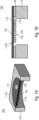
- FIGS 1A and 1B show a first embodiment of a MEMS device 100 according to the herein described innovative concept.
- the MEMS device 100 comprises a substrate 110.
- the substrate 110 may comprise or be made from silicon.
- the substrate 110 comprises a vertically extending cavity 116 that may extend completely through the substrate 110.
- the MEMS device 100 further comprises a horizontally extending membrane structure 130.
- the membrane structure 130 may comprise or be made from polysilicon.
- the membrane structure 130 covers the cavity 116.
- the membrane structure 130 may be created from a membrane material layer 114 being deposited on a sacrificial layer 140 (e.g., TEOS: tetraethoxysilane or tetraethyl orthosilicate).
- a sacrificial layer 140 may be sandwiched between the substrate 110 and the membrane material layer 114 and may connect the membrane structure 130 with the substrate 110.
- the membrane structure 130 may be adhered to the substrate 110, e.g., by means of an adhesive.
- a plurality of upright (e.g., vertically extending) nanostructures 150 is created in the membrane material layer 114 by applying a laser structuring process, such that the nanostructures 150 protrude from at least one of two opposing membrane surface 114A, 114B.
- the horizontally extending membrane material layer 114 comprises a first membrane surface 114A facing the cavity 116, and an opposite second membrane surface 114B facing away from the cavity 116.
- the protruding nanostructures 150 may be arranged on the first membrane surface 114A. Additionally or alternatively, the protruding nanostructures 150 may be arranged on the second membrane surface 114B. This holds for each and every embodiment as discussed herein.
- the protruding nanostructures 150 are created by applying a laser structuring process, as will be discussed in more detail later with reference to Figures 11A to 16 . Therefore, the nanostructures 150 may be monolithically integrated in the membrane material layer 114. Accordingly, the membrane material layer 114 forms a free-standing membrane structure 130 with integrated protruding nanostructures 150.
- the protruding nanostructures 150 may extend substantially perpendicular to the membrane structure 130.
- the protruding nanostructures 150 provide for a self-cleaning surface characteristic exploiting the so-called lotus effect. Accordingly, the protruding nanostructures 150 provide for a liquid repellent membrane surface of the membrane structure 130.
- the protruding nanostructures 150 create a rough nanostructured membrane surface 114A, 114B that may provide for at least one of a hydrophobic or an oleophobic surface characteristic of the membrane structure 130.
- a membrane without these protruding nanostructures 150 may comprise a hydrophilic surface characteristic, i.e., liquids (water, oil, etc.) adhere to the membrane. If the liquid evaporates, solid matters (like salts, particles, and other contaminants) that are solved in said liquids, may remain on the membrane surface which may often result in device contamination, corrosion and/or electrical shortcut (leakage).
- the membrane structure 130 of the herein described innovative concept instead, comprises a hydrophobic and/or oleophobic surface characteristic, i.e., liquids (water, oil, etc.) are repelled from the membrane structure 130. Said hydrophobic and/or oleophobic surface characteristics are provided by the protruding nanostructures 150.
- the MEMS device 100 as depicted in Figures 1A and 1B may be configured as a discrete environmental barrier structure, e.g., an environmental barrier mesh or membrane.
- Such environmental barrier structures 100 may be used in connection with MEMS microphones in order to protect the thin and fragile microphone membrane from ingress of environmental particles, moisture and other physical and/or chemical objects. Details will be discussed later with reference to Figures 10A to 10C .
- FIGS 2A and 2B show a further embodiment of a MEMS device 100.
- a so-called single backplate (SBP) MEMS-based microphone 100 is shown.
- the single backplate microphone 100 comprises an electrode structure 160 that can be electrically connected, e.g., by means of pads / terminals 170, to a circuitry (not shown).
- the electrode structure 160 may comprise or be made from silicon nitride, Si 3 N 4 .
- the membrane structure 130 may be configured as a microphone membrane that can oscillate in response to acoustic waves.
- the acoustic waves may enter the microphone package through a so-called sound port.
- the depicted single backplate microphone 100 may be mounted over the sound port, such that the acoustic waves may enter the vertically extending cavity 116 and arrive at the bottom surface of the membrane structure 130.
- the upright (e.g., vertically extending) nanostructures 150 which protrude from the membrane structure 130, may provide for a hydrophobic / oleophobic surface characteristic of the membrane structure 130.
- liquids contained in the air that is transferred by the acoustic waves may be repelled from the hydrophobic and/or oleophobic membrane surface.
- the protruding nanostructures 150 are provided at a membrane surface that faces a source of environmental liquids, for example the sound port.
- the protruding nanostructures 150 may face the cavity 116 and may vertically extend into the cavity 116.
- the protruding nanostructures 150 may additionally or alternatively face away from the cavity 116 and may vertically extend away from the cavity 116.
- the protruding nanostructures 150 may be arranged on either one of the two membrane surfaces 114A, 114B or on both membrane surfaces 114A, 114B.
- FIGS 3A and 3B show a further embodiment of a MEMS device 100.
- a so-called sealed dual-membrane (SDM) MEMS-based microphone 100 is shown.
- the sealed dual-membrane microphone 100 comprises a membrane structure 130 having a first membrane portion 131 and a second membrane portion 132.
- An electrode structure 160 is sandwiched between the first and second membrane portions 131, 132. While the membrane portions 131, 132 may be flexible, the electrode structure 160 may be a rigid electrode structure, such as a backplate or a stator, for example.
- At least one of the first and second membrane portions 131, 132 may comprise the above described upright nanostructures 150 that protrude from the respective membrane portion 131, 132. Also in this case, it is advantageous if the protruding nanostructures 150 are provided at a membrane surface that faces a source of environmental liquids, for example the sound port. Thus, in this non-limiting example, the protruding nanostructures 150 may be arranged on the second membrane portion 132 facing the cavity 116.
- the protruding nanostructures 150 may be configured as upright (e.g., vertically extending) nanospikes, nanotubes, nanofins, nanopillars, nanowhiskers, nanowalls, nanocircular walls, black silicon, and many more, while various other geometric designs and shapes are possible.
- the protruding nanostructures 150 may be configured as single, free-standing 3D elements, that protrude from a plane surface, e.g, from at least one of the two opposing membrane surfaces 114A, 114B of the membrane structure 130.
- the protruding nanostructures 150 may not be connected to each other, i.e., they are configured as individual unconnected elements. This is a difference compared to meshes and grids, which may sometimes be used as environmental barrier structures.
- Meshes and grids comprise a plurality of single mesh segments / grid segments that are all connected to each other to form the mesh / grid structure.
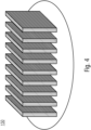
- Figures 4 to 6 show some non-limiting examples of protruding nanostructures 150 being configured as single free-standing and unconnected 3D elements.
- Figure 4 shows protruding nanostructures 150 being configured as single free-standing and unconnectedupright walls or plates being consecutively arranged along a (straight or curved) line.
- Figure 5 shows protruding nanostructures 150 being configured as single free-standing and unconnected concentric walls.
- Figure 6 shows protruding nanostructures 150 being configured as single free-standing and unconnected (hollow) nanotubes.
- the protruding upright nanostructures 150 may be configured as single unconnected three-dimensional geometric structures extending away from the membrane structure 130.
- the protruding upright nanostructures 150 may extend into a direction that is substantially perpendicular to the lateral extension of the membrane structure 130.
- the single unconnected nanostructures 150 may be configured as single upright nanopillars protruding and extending away from the membrane structure 130.
- Nanopillars are pillar-shaped nanostructures, approximately a few nanometers (e.g. 10 nm to 1.000 nm) in diameter, that can be grouped together in lattice like arrays.
- the protruding nanostructures 150 may be densely arranged next to each other.
- the plurality of protruding nanostructures 150 may comprise an area density of 10 6 - 10 10 nanostructures per cm 2 .
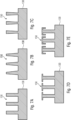
- the protruding nanostructures 150 may comprise a geometrical shape similar to a frustum cone.
- the upright nanostructures 150 may comprise a geometrical shape similar to a straight cylinder protruding from the membrane structure 130.
- the upright nanostructures 150 may comprise a geometrical shape similar to a frustum cone protruding from the membrane structure 130.
- the upright nanostructures 150 may comprise a geometrical shape similar to an inverted frustum cone protruding from the membrane structure 130.
- the upright nanostructures 150 may comprise a T-shape, i.e., a geometrical shape similar to the letter 'T', and they may protrude from the membrane structure 130.
- the upright nanostructures 150 may comprise a multifaceted T-shape, i.e., a geometrical shape similar to the letter 'T' with additional contoured walls (e.g., reentrant structure), and they may protrude from the membrane structure 130.
- the different geometrical shapes may lead to different hydrophobic and/or oleophobic surface characteristics of the protruding nanostructures 150.
- FIG. 8 shows an embodiment, wherein the protruding nanostructures 150 may be coated with organic self-assembled monolayers.
- Nanostructures 150 being coated with SAMs exhibit an enhanced level of hydrophobicity and/or oleophobicity compared to uncoated nanostructures 150.
- the SAM-coated nanostructures 150 can increase the resulting water or liquid contact angle on their surface and can repel not only water but also other liquids (e.g., oil) resulting in (super-)hydrophobic or omniphobic surfaces.
- the organic self-assembled monolayers may comprise, or may consist of, at least one of:
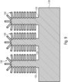
- Figure 9 shows a further embodiment, wherein the protruding nanostructures 150 may comprise inorganic nano-elements 190, e.g., nanodots or nanowires, protruding from a surface of the nanostructures 150.
- Nanostructures 150 comprising additional nano-elements 190 exhibit an enhanced level of hydrophobicity and/or oleophobicity compared to bare/naked nanostructures 150.
- the inorganic nano-elements 190 may be grown on the surface of the nanostructures 150.
- a suitable material for example zinc oxide (ZnO)
- ZnO zinc oxide
- a zinc oxide film may be deposited onto the surface of the nanostructures 150 using e.g., a sputtering technique for forming ZnO nanoseeds.
- the growth of the ZnO nanowires can then be realized by employing e.g., a chemical bath deposition (CBD) process.
- CBD chemical bath deposition
- ZnO nano-elements 190 may be advantageously grown on silicon-based nanostructures 150.
- the grown nano-elements 190 may protrude from the nanostructures 150, and they may extend substantially perpendicular from the surface of the nanostructures 150. Accordingly, the nanostructures 150 may comprise a tree-like shape. Each of the tree-like nanostructures 150 may comprise a plurality of inorganic nano-elements 190, e.g., nanowires.
- the nanostructures 150 may provide for a hydrophobic and/or oleophobic and/or superhydrophobic and/or omniphobic surface characteristic of the membrane structure 130.
- Planar silicon surfaces in general comprise a hydrophilic surface characteristic, i.e., liquids are adhered to the planar surface due to its low surface roughness and, thus, its large surface energy.
- a hydrophilic surface comprises a small water contact angle.
- the water contact angle may be around 5° to 20°.
- a nanostructured silicon surface for example the herein described rough nanostructured membrane surfaces 114A, 114B of the membrane structure 130 with the protruding nanostructures 150, may comprise a larger water contact angle of at least 120° or at least 150°. Therefore, a water droplet being applied to the nanostructured membrane surface 114A, 114B almost stays in a perfect sphere shape. This is due to the higher surface roughness and, thus, lower surface energy provided by the nanostructures 150. Accordingly, the membrane structure 130 comprising the protruding nanostructures 150 may comprise a hydrophobic or even superhydrophobic surface characteristic.
- Superhydrophobic surfaces generally show water contact angles of greater than 150° (nearly perfect sphere) along with low contact angle hysteresis.
- Contact angle hysteresis is defined as the difference between measured values of the advancing and receding contact angles (the highest and lowest contact angles on such a structures).
- the nanostructures 150 protruding from the membrane structure 130 may provide an oleophobic surface characteristic such that oils are repelled from the membrane surface, or even an omniphobic surface characteristic such that almost each and every liquid is repelled from the membrane surface.
- nanostructured membrane 130 Liquids that approach the nanostructured membrane 130 having superhydrophobic/omniphobic surface characteristics will bounce or roll off.
- the herein discussed nanostructures 150 are useful for water/liquid repellent and self-cleaning surfaces.
- the nanostructured membrane surface can be self-cleaning because any water/liquid droplets that contact it will roll off picking up any particles along with the operation of the moving membrane 130.
- the hydrophobicity / oleophobicity / omniphobicity level of the nanostructures 150 can be varied.
- nanostructures 150 with high aspect ratio e.g., x > 5 produce a larger contact angle (more hydrophobicity / omniphobicity) than those with low aspect ratio (e.g., 1 ⁇ x ⁇ 5).
- the MEMS device 100 may be configured as a MEMS-based microphone or as a discrete MEMS-based environmental barrier.
- the MEMS device 100 may be housed underneath a lid so as to produce a MEMS-based package, e.g., a microphone package.
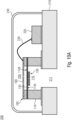
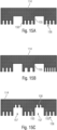
- FIG 10A shows a first embodiment of a MEMS-based package 200.
- the package 200 may comprise a component board 210, e.g., a printed circuit board (PCB).
- a MEMS device 100 according to the herein described innovative concept may be arranged on the component board 210.
- a circuitry 220 for controlling the MEMS device 100 may be arranged adjacent to the MEMS device 100.
- the MEMS device 100 may be electrically connected to the circuitry 220, for example by means of a bond wire 230.
- the package 200 may further comprise a lid 240 being arranged on the component board 210.
- the lid 240 may cover the MEMS device 100 and the circuitry 220.
- the free space or cavity 250 underneath the hollow lid 240 may provide for an acoustic back volume.
- the component board 210 may comprise a vertically extending through hole 211.
- the through hole 211 may be referred to as a sound port through which acoustic waves may enter the cavity 250.
- the MEMS device 100 may be configured as a MEMS-based single backplate (SBP) microphone, as previously discussed above with reference to Figures 2A and 2B .
- the horizontally extending membrane structure 130 may be configured as a microphone sound transducer membrane, wherein the upright nanostructures 150 protrude from the microphone sound transducer membrane 130.
- the protruding nanostructures 150 may be arranged on the first membrane surface 114A facing the through hole (sound port) 211.
- the protruding nanostructures 150 may be arranged on the opposite second membrane surface 114B facing away from the through hole (sound port) 211.
- the SBP microphone 100 is arranged directly opposite to the sound port 211, e.g., above the sound port 211.
- the SBP microphone 100 is arranged such that it covers the sound port 211.
- the horizontally extending membrane structure 130 circumferentially covers the sound port 211.
- the protruding nanostructures 150 face the sound port 211.
- acoustic waves may enter the package 200 through the sound port 211. Since the sound port 211 is in fluid connection with the cavity 116, the acoustic waves may be further conveyed into the cavity 116 until reaching the membrane structure 130. The membrane structure 130 will be deflected in response to the impinging acoustic waves. The amplitude of deflection will be measured by the electrode structure 160.
- the air through which the acoustic waves may travel may comprise moisture, e.g., liquids containing salt particles and the like. Since the herein described innovative membrane structure 130 comprises the protruding nanostructures 150, the membrane structure 130 shows a (super-)hydrophobic / omniphobic surface characteristic. Thus, intruding liquids and or any solid matter (like salts, particles, and other contaminants) contained in said liquids may be repelled from the surface of the membrane structure 130. This provides for a superior protection of the microphone membrane 130.
- FIG. 10B shows a further embodiment of a MEMS-based package 200 being configured as a microphone package.
- MEMS device 100 is configured as a sealed dual-membrane (SDM) MEMS-based microphone.
- SDM sealed dual-membrane
- FIG 10C shows a further embodiment of a MEMS-based package 200.
- the MEMS device 100 according to the herein described innovative principle may be configured as a discrete MEMS-based environmental barrier structure. For details as to any elements comprised by said environmental barrier 100, it is referred to Figures 1A and 1B above.
- a MEMS-based microphone 300 is depicted.
- This MEMS-based microphone 300 may be a MEMS device 100 as discussed above, or a conventional MEMS-based microphone.
- a conventional SDM microphone is depicted.
- a SBP microphone may be used instead.
- the MEMS-based microphone 300 may comprise a microphone sound transducer membrane 310.
- the innovative MEMS device 100 may be arranged between the sound port 211 and the MEMS-based microphone 300.
- the MEMS device 100 being configured as an environmental barrier structure acts as an environmental barrier for protecting the MEMS microphone sound transducer membrane 310 from moisture and/or environmental particles.
- the MEMS device 100 being configured as an environmental barrier structure comprises a horizontally extending environmental barrier membrane or mesh structure.
- the innovative membrane structure 130 may be configured as the aforementioned environmental barrier membrane or mesh structure.
- the membrane structure 130 may comprise the protruding nanostructures 150 as discussed herein. This provides for an improved hydrophobicity / omniphobicity level of the membrane structure 130. Thus, intruding liquids and or any solid matter (like salts, particles, and other contaminants) contained in said liquids may be repelled from the surface of the membrane structure 130. This provides for a superior protection of the downstream arranged microphone membrane 310.
- Figures 11A to 11F show an embodiment of a method for fabricating a MEMS device 100 as discussed herein.
- the above discussed protruding nanostructures 150 are created by applying a laser structuring process, as will be described in more detail below.
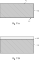
- Figure 11A shows a first method step, wherein a substrate 110 is provided, the substrate 110 comprising a first substrate surface 111 and an opposite second substrate surface 112.
- the substrate 110 may comprise or consist of silicon.
- Figure 11B shows a further method step, wherein a sacrificial layer 140 is arranged at the first substrate surface 111.
- the sacrificial layer 140 may comprise or consist of tetraethoxysilane (TEOS).
- TEOS tetraethoxysilane
- the sacrificial layer 140 may comprise or consist of one or more oxides.
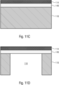
- FIG 11C shows a further method step, wherein a membrane material layer 114 is deposited onto the sacrificial layer 140.
- a membrane material layer 114 may comprise or be made from one or more materials that are suitable for providing a MEMS-membrane, e.g., polysilicon.
- Figure 11D shows a further method step, wherein a cavity 116 is structured into the substrate 110.
- the cavity 116 may be created by applying a suitable etching process, such as RIE or DRIE etching.
- the cavity 116 may extend between the second substrate surface 112 and the sacrificial layer 140.
- the cavity 116 may have the shape of a through hole that extends completely through the substrate 110 between the first and second substrate surfaces 111, 112.
- Figure 11E shows a further method step, wherein the membrane material layer 114 is released by removing the sacrificial layer 140 from the cavity 116, i.e. portions of the sacrificial layer 140 that were previously sitting inside the cavity (c.f. Figure 11D ) are removed, such that only residual portions of the sacrificial layer 140 may remain between substrate portions and the membrane material layer 114.
- the sacrificial layer 140 may be removed by applying a suitable etching process, such as a chemical wet etching process. After removing the above mentioned portions of the sacrificial layer 140, the cavity 116 is directly adjacent to the membrane material layer 114. Accordingly, the released membrane material layer 114 forms a free-standing membrane structure 130 covering the cavity 116.
- Figure 11F shows a further method step, wherein nanostructures 150 are created in at least one of the first and second membrane surfaces 114A, 114B of the membrane material layer 114.
- the nanostructures 150 are created by applying a laser structuring process, wherein laser beams are schematically represented by arrows 180.
- the laser structuring can be applied prior to or after the step of releasing the membrane layer 114 ( Fig. 11E ).
- the applied laser structuring process may use a femto second laser or a pico second laser. This may have the advantage that membrane material may change from solid to gas, without an intermediate liquid state, and heat input may be limited to specific spots.
- the nanostructures 150 may be formed from the membrane material layer 114, or in other words, the nanostructures 150 may be monolithically integrated in the membrane material layer 114.
- the step of creating the nanostructures 150 may comprise a step of removing portions 118 of the membrane material layer 114 by means of one or more laser beams 180 being used in the applied laser structuring process, wherein the nanostructures 150 remain between the removed portions 118 of the membrane material layer 114, such that the nanostructures 150 are monolithically integrated in the membrane material layer 114.
- the applied laser structuring process may comprise Direct Laser Interference Patterning (DLIP), wherein interference patterns may be directly imprinted into the membrane surface 114A, 114B of the membrane material layer 114.
- DLIP Direct Laser Interference Patterning
- the step of creating the nanostructures 150 may comprise distributing the nanostructures 150 in a random or periodic pattern along the respective membrane surface 114A, 114B of the membrane material layer 114.
- the nanostructures 150 that are created according to the herein described innovative principle are not only monolithically integrated in the membrane material layer 114, but they also protrude from the respective membrane surface 114A, 114B of the membrane material layer 114.
- the protruding nanostructures 150 provide for an increased surface roughness (compared to unstructured plane membrane surfaces without nanostructures) of the respective membrane surface 114A, 114B thereby increasing the hydrophobicity and/or oleophobicity level of the membrane material layer 114 and, thus, of the membrane structure 130 created therefrom.
- the nanostructures 150 are created in the first membrane surface 114A of the membrane material layer 114, said first membrane surface 114A facing the cavity 116, such that the nanostructures 150 also face the cavity 116.
- the one or more laser beams 180 is/are guided into the cavity 116 so as to reach the first membrane surface 114A of the membrane material layer 114 through the cavity 116. This may be performed as a last process step in the frontend production leading to a simplified processing of creating the protruding nanostructures 150 compared to other processes, such as lithography processes.
- Figure 12 shows an alternative method step, wherein the protruding nanostructures 150 are created in the second membrane surface 114B, said second membrane surface 114B facing away from the cavity 116, such that the nanostructures 150 also face away from the cavity 116.
- the one or more laser beams 180 is/are guided over the second membrane surface 114B of the membrane material layer 114.
- the protruding nanostructures 150 may be created in the first and second membrane surfaces 114A, 114B.
- Figure 13A shows an optional method step, wherein the one or more laser beams 180 being used in the applied laser structuring process is/are guided over an exposed portion 112A of the second substrate surface 112 that remains after creating the cavity 116. Accordingly, the remaining exposed portion 112A is located outside the cavity 116, such that additional nanostructures 151 are created in said exposed portions 112A of the second substrate surface 112.
- the additional nanostructures 151 may be formed integrally / monolithically with the laser-treated exposed portions 112A of the second substrate surface 112.
- the additional nanostructures 151 may protrude from the laser-treated exposed portions 112A of the second substrate surface 112 thereby increasing their surface roughness leading to an increased hydrophobicity / olephobicity.
- Figure 13B shows a further optional method step, wherein the one or more laser beams 180 being used in the applied laser structuring process is/are guided over one or more inner substrate portions 110A (e.g., inner side walls) residing inside the cavity 116, such that additional nanostructures 152 are created in said one or more inner substrate portions 110A.
- the additional nanostructures 152 may be formed integrally / monolithically with the laser-treated inner substrate portions 110A.
- the additional nanostructures 152 may protrude from the laser-treated inner substrate portions 110A thereby increasing their surface roughness leading to an increased hydrophobicity / olephobicity.
- Figure 13C shows a further alternative, wherein the additional protruding nanostructures 151, 152 may be created in the exposed portions 112A of the second substrate surface 112 and in the inner substrate portions 110A residing inside the cavity 116.
- Figures 14A and 14B show a further embodiment of a method for producing the above discussed innovative MEMS device 100.
- This method is a combined method in which lithography is combined with laser structuring.
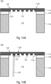
- the method comprises a step of creating nanopillars 155 in at least one of the first and second membrane surfaces 114A, 114B of the membrane material layer 114 by applying a lithography and etching process, wherein said nanopillars 155 protrude from the respective membrane surface 114A, 114B of the membrane material layer 114.
- the nanopillars 155 being created by lithography are formed in the first membrane surface 114A.
- the nanostructures 150 are then created in said nanopillars 155 by applying the above discussed laser structuring process, wherein the laser beams are schematically depicted by means of arrows 180.
- the laser structured nanostructures 150 are created in a top surface 156 of the nanopillars 155, wherein said top surface 156 faces away from the membrane material layer 114, i.e. it faces the cavity 116.
- the laser structured nanostructures 150 protrude from the nanopillars 155 created in the membrane material layer 114 by means of lithography and, as such, the nanostructures 150 protrude from the membrane material layer 114.
- the nanopillars 155 created by lithography may comprise an average diameter that is at least ten times larger than an average diameter of the laser structured nanostructures 150.
- the nanopillars 155 may comprise a diameter of 100 nm
- the laser structured nanostructures 150 may comprise a diameter of 10 nm.
- Figures 15A to 15C show some non-limiting examples of laser structured nanostructures 150 and how they can be structured into the nanopillars 155 by applying the laser structuring process.
- Figure 15A shows a first example that corresponds to the embodiment described above with reference to Figure 14B .
- the laser structured nanostructures 150 are created in the top surface 156 of the nanopillars 155.
- Figure 15B shows a further example, wherein the laser structured nanostructures 150 comprise different sizes.
- the laser structured nanostructures 150 may comprise different diameters.
- the laser structured nanostructures 150 may be arranged more or less densely among each other. This may apply to each and every embodiment discussed herein.
- Figure 15C shows a further example, wherein the step of creating the nanostructures 150 by applying the laser structuring process comprises a step of creating the nanostructures 150 in a recess 157 between two adjacent nanopillars 155.
- the laser structured nanostructures 150 may be created inside the recess 157 in addition to the creation of laser structured nanostructures 150 in the top surfaces 156 of the nanopillars 155.
- the laser structured nanostructures 150 may be created inside a recess 157only, i.e. without any laser structured nanostructures 150 being provided in the top surfaces 156 of the nanopillars 155.
- the nanopillars 155 may also be referred to as nanowhiskers.
- the above discussed nanopillars 155 may comprise a geometrical shape that is different to a pillar.
- they may generally be referred to as nanopillars 155 within this disclosure.
- the nanopillars 155 have been described as being created by means of lithography, other embodiments may include that the nanopillars 155 are created differently, for example also by means of laser structuring, or the nanopillars 155 may be deposited onto at least one of the membrane surfaces 114A, 114B.
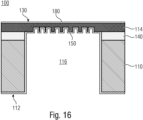
- Figure 16 shows a further embodiment of the innovative method for producing a MEMS device 100.
- the method may further comprise a step of coating the membrane material layer 114, including the protruding nanostructures 150, with an organic Self Assembled Monolayer - SAM - 180, similar as described above with reference to Figure 8 .
- the SAM-coating 180 may further coat the inside of the cavity 116 and/or the exposed second substrate surface 112. Further optionally, the SAM-coating 180 may coat the entire MEMS device 100.
- SAMs 180 may provide for an advanced surface chemistry modification of the coated surfaces.
- nanostructures 150 being coated with SAMs exhibit an enhanced level of hydrophobicity and/or oleophobicity compared to uncoated nanostructures 150.
- the SAM-coated nanostructures 150 can increase the resulting water or liquid contact angle on their surface and can repel not only water but also other liquids (e.g., oil) resulting in (super-)hydrophobic or omniphobic surfaces.
- Different self-assembled monolayers, and in particular silane-based SAMs may be used for coating the protruding nanostructures 150.
- the laser structured nanostructures 150 improve hydrophobicity and/or oleophobicity of a treated surface, which expresses in a higher contact angle of 120° or more, or even 150° or more. Furthermore, SAMs do also improve hydrophobicity and/or oleophobicity of the treated surface.
- the authors of the present disclosure surprisingly found out that the laser structured nanostructures 150 can improve the hydrophobicity / oleophobicity effect of SAMs. Accordingly, the laser structured nanostructures 150 in combination with SAMs do provide for an increased hydrophobicity / oleophobicity effect compared to SAMs alone or compared to nanostructures 150 alone. In other words, the combination of laser structured nanostructures 150 with SAMs lead to a higher contact angle compared to SAMs alone or compared to nanostructures 150 alone.
- the herein discussed innovative laser structured nanostructures 150 may comprise a characteristic geometrical shape that allows to distinguish them from nanostructures 150 that have been created by methods different from laser structuring.
- nanostructures 150 may also be created by lithography, deposition or growing, as will be discussed in more detail below with reference to Figures 17A to 20H .
- laser structured nanostructures 150 may comprise a non-flat top section, e.g., a sharp top. Furthermore, due to the laser beams 180 being applied to the membrane material layer 114 in slightly varying angles, the laser structured nanostructures 150 of two different MEMS devices 100 may comprise a similar pattern (in terms of roughness etc.) but with different orientations towards each other, i.e., offsets may not be exactly identical. Nanostructures being created by means of lithography, for instance, may comprise an identical pattern instead. Yet further, nanostructures being created by means of lithography may comprise a shape that is limited to certain angles around 90°. In turn, the shape of laser structured nanostructures 150 may differ from 90° and may vary.
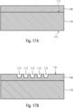
- Figures 17A to 17F show an embodiment of an exemplary method for fabricating a MEMS device 100, wherein the nanostructures 150 may be created by means of lithography.
- a substrate 110 is provided, the substrate 110 comprising a first substrate surface 111 and an opposite second substrate surface 112.
- the substrate 110 may comprise or consist of silicon.
- a sacrificial layer 140 may be arranged at the first substrate surface 111.
- the sacrificial layer 140 may comprise or consist of tetraethoxysilane (TEOS).
- TEOS tetraethoxysilane
- the sacrificial layer 140 may comprise or consist of one or more oxides.
- the sacrificial layer 140 may be structured / patterned, e.g., by using a lithography process.
- so-called nanoimprints 113 may be structured into the sacrificial layer 140.
- the nanoimprints 113 may be structured into an upper surface 141 of the sacrificial layer 140, i.e., into a surface of the sacrificial layer 140 that faces away from the substrate 110.
- Figure 17C shows a further method step in which the nanoimprints 113 are filled with a first material 114, e.g., by using a deposition process, in which the first material 114 is deposited onto the structured sacrificial layer 140.
- the first material 114 may later form the membrane structure 130 with integrated protruding nanostructures 150 (c.f. Fig. 17F ).
- the first material 114 may also be referred to as a membrane material layer 114, as described above.
- the first material 114 may comprise or consist of a CMOS-compatible material (CMOS: Complementary Metal-Oxide-Semiconductor).
- CMOS Complementary Metal-Oxide-Semiconductor
- the first material 114 may comprise or consist of at least one of (poly-)silicon, silicon nitride (Si 3 N 4 ), carbon, polymers and metals.
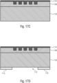
- Figure 17D shows a further method step, wherein a photoresist 115 is applied to the second surface 112 of the substrate 110.
- the photoresist 115 provides a negative form for a cavity 116 that is created in the next step, as shown in Figure 17E .
- a portion of the second substrate surface 112 that is located opposite to the filled nanoimprints 113 remains uncovered, i.e., it is not covered with the photoresist 115.
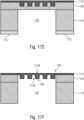
- Figure 17E shows a further method step, in which the cavity 116 is structured into substrate 110.
- the cavity 116 is structured into that portion of the second substrate surface 112 that is not covered by the photoresist 115.
- the cavity 116 is structured through the entire substrate 110 until reaching the sacrificial layer 140.
- the cavity 116 may be structured into the substrate 110 by using reactive ion etching (RIE).
- RIE reactive ion etching
- the created cavity 116 is positioned opposite to the filled nanoimprints 113, and the created cavity 116 extends between the second substrate surface 112 and the sacrificial layer 140.
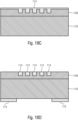
- Figure 17F shows a further method step, in which the filled nanoimprints 113 are released by selectively removing the sacrificial layer 140 through the cavity 116.
- a RIE or wet chemical etching process may be used for selectively removing portions of the sacrificial layer 140 that are located inside the cavity 116.
- the (meanwhile released) first material 114 forms a horizontally extending membrane structure 130.
- Any of the first material 114 that was previously filled inside the (meanwhile released) nanoimprints 113 form upright (e.g., vertically extending) nanostructures 150 protruding from at least one of the membrane surfaces 114A, 114B of the membrane structure 130, as discussed above.
- the membrane structure 130 and the protruding nanostructures 150 are made from the same (first) material 114, the membrane structure 130 and the protruding nanostructures 150 are integrally formed. Furthermore, as exemplarily depicted here, the protruding nanostructures 150 may face and extend into the cavity 116.
- the nanoimprints 113 may provide a negative form for the protruding nanostructures 150 (c.f. Figure 17F ).
- the diameter, pitch and aspect ratio of the nanoimprints 113 correspond to the desired diameter, pitch and aspect ratio of the nanostructures 150 in order to provide the desired (super-)hydrophobic / omniphobic surface characteristics.
- the horizontally extending membrane structure 130 and the protruding nanostructures 150 may be made from the same (first) material 114.
- the first material 114 forming the membrane structure 130 and the integrally formed protruding nanostructures 150 may comprise a conducting or semiconducting characteristic.
- the first material 114 may comprise or consist of (poly-)silicon.
- the first material 114 forming the membrane structure 130 and the integrally formed protruding nanostructures 150 may comprise a dielectric characteristic.
- the first material 114 may comprise or consist of silicon nitride or one or more oxides. Dielectric nanostructures 150 may be beneficial if electrical leakages shall be avoided.
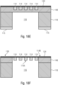
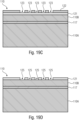
- Figures 18A to 18F show an alternative method for fabricating a MEMS device 100, wherein the nanostructures 150 are also created by means of lithography.
- Like elements with like features, as discussed with reference to Figures 17A to 17F are indicated with same reference numerals. Accordingly, for further details it is referred to the above discussion.
- a difference compared to the above discussed embodiment starts at Figure 18D .
- the deposited first material 114 is removed from the sacrificial layer 140, while the deposited first material 114 residing inside the nanoimprints 113 is maintained. Accordingly, only the first material 114 that resides inside the nanoimprints 113 remains after this process step. In other words, the nanoimprints 113 being filled with the first material 114 remain, while the rest of the first material 114 is removed.
- Figure 18E shows a further method step, wherein a different second material 124 is deposited onto the sacrificial layer 140 including the filled nanoimprints 113.
- the first material 114 residing inside the nanoimprints 113 and the deposited second material 124 may combine and/or adhere to each other.
- a cavity 116 may be structured into substrate 110, in the way as described above with reference to Figure 17E .
- Figure 18F shows a further method step, in which the nanoimprints 113 being filled with the first material 114 and the deposited layer of the second material 124 are released by selectively removing the sacrificial layer 140 through the cavity 116.
- a RIE process may be used for selectively removing portions of the sacrificial layer 140 that are located inside the cavity 116.
- the (meanwhile released) second material 124 forms a horizontally extending membrane structure 130.
- Any of the first material 114 that was previously filled inside the (meanwhile released) nanoimprints 113 form upright (e.g., vertically extending) nanostructures 150 protruding from at least one of the membrane surfaces 114A, 114B of the membrane structure 130, as discussed above.
- the horizontally extending membrane structure 130 is made from the subsequently deposited second material 124, and the protruding nanostructures 150 are made from the first material 114.
- the membrane structure 130 and the protruding nanostructures 150 may be firmly bonded.
- the protruding nanostructures 150 may face and extend into the cavity 116.
- the second material 124 forming the membrane structure 130 may comprise a conducting or semiconducting characteristic.
- the second material 124 may comprise or consist of (poly-)silicon.
- the first material 114 forming the protruding nanostructures 150 may comprise a dielectric characteristic.
- the first material 114 may comprise or consist of silicon nitride (Si 3 N 4 ) or one or more oxides. Dielectric nanostructures 150 may be beneficial if electrical leakages shall be avoided.
- the horizontally extending membrane structure 130 and the protruding upright nanostructures 150 may be made from different materials.
- a (semi-)conducting membrane structure 130 may be provided, which comprises dielectric nanostructures 150.
- the above embodiments concern methods for creating a horizontally extending membrane structure 130 with protruding upright (e.g., vertically extending) nanostructures 150, wherein said protruding nanostructures 150 faced the cavity 116.
- some further embodiments will be described which provide for a method for creating a horizontally extending membrane structure 130 with protruding upright (e.g., vertically extending) nanostructures 150, wherein said protruding nanostructures 150 face away from the cavity 116.
- these embodiments may be combined with each other, e.g., for creating a first set of protruding nanostructures 150 facing the cavity 116 in combination with a second set of protruding nanostructures 150 facing away from the cavity 116.
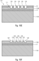
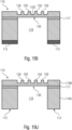
- Figures 19A to 19J show an embodiment for creating protruding nanostructures 150 according to a top-down approach. Like elements with like features, as discussed with reference to the above Figures, are indicated with same reference numerals. Accordingly, for further details it is referred to the above discussion.
- a substrate 110 is provided having a first substrate surface 111 and an opposite second substrate surface 112.
- the substrate 110 may comprise or consist of silicon.
- a silicon-on-insulator (SOI) substrate is shown, which may comprise an insulating layer 117.
- the insulating layer 117 is optional.
- the insulating layer 117 may comprise or consist of one or more oxides, for example silicon oxide (SiO 2 ).
- the insulating layer 117 may divide the substrate 110 into a first substrate portion 110A and a second substrate portion 110B.
- Figure 19B shows a further method step, wherein a material layer 121 is deposited onto the first substrate surface 111.
- the material layer 121 may comprise or consist of tetraethoxysilane (TEOS).
- TEOS tetraethoxysilane
- the material layer 121 may comprise or consist of one or more oxides.
- Figure 19C shows a further method step, wherein a thin photoresist 122 is applied onto the material layer 121.
- the photoresist 122 may be nanopatterned for creating a pattern with a plurality of openings 123 having dimensions in the range of nanometers.
- the nanopatterned photoresist 122 may provide a negative form for patterning the adjacent material layer 121 underneath.
- Figure 19D shows a further method step, wherein the material layer 121 is patterned by means of the photoresist 122. Accordingly, the nanopattern of the photoresist 122 is transferred to the material layer 121 such that the material layer 121 comprises a pattern with a plurality of openings 125 having dimensions in the range of nanometers.
- Figure 19E shows a further method step, wherein the first substrate surface 111 is structured using the nanopatterned material layer 121 as a mask.
- Vertical openings 126 are structured into the first substrate surface 111, e.g., by using a RIE process.
- the openings 126 may extend vertically into the substrate 110.
- the openings 126 may comprise dimensions in the range of nanometers.
- Figure 19F shows a further method step, wherein the material layer 121 is removed from the substrate 110.
- the first substrate surface 111 is structured as described above, i.e., it comprises a pattern with a plurality of openings 126 having dimensions in the range of nanometers. Substrate material remaining laterally between adjacent openings 126 forms upright (e.g., vertically extending) nanostructures 150.
- Figure 19G shows a further method step, wherein a thick negative photoresist 115 is applied to the second substrate surface 112.
- the photoresist 115 provides a negative form for a cavity 116 that is created in the next step, as shown in Figure 13H.
- a portion of the second substrate surface 112 that is located opposite to the upright nanostructures 150 remains uncovered, i.e., it is not covered with the photoresist 115.
- Figure 19H shows a further method step, in which the cavity 116 is structured into substrate 110.
- the cavity 116 is structured into that portion of the second substrate surface 112 that is not covered with the photoresist 115. Accordingly, the cavity 116 is positioned opposite to the upright nanostructures 150.
- the cavity 116 is not structured through the entire substrate 110. Instead, the cavity 116 is structured such that it stops before reaching the nanostructures 150. Accordingly, a substrate portion 110C between the nanostructures 150 and the cavity 116 remains. This remaining substrate portion 110C may later form the horizontally extending membrane structure (c.f. Figure 19J ) from which the nanostructures 150 protrude. The remaining substrate portion 110C may comprise a thickness of only a few nanometers (e.g., between 300 nm and 1.100 nm).
- the substrate 110 may comprise an optional etch stop layer 117. If the etch stop layer 117 is available, as exemplarily depicted in Figure 19H , the cavity 116 may be structured until reaching the etch stop layer 117. However, if the etch stop layer 117 is not available, the structuring process of creating the cavity 116 may be precisely controlled such that the above mentioned substrate portion 110C remains between the cavity 116 and the nanostructures 150.
- Figure 19I shows a further optional method step, wherein the optional etch stop layer 117 is removed inside the cavity 116 for releasing the above discussed remaining substrate portion 110C.
- the remaining substrate portion 110C forms the horizontally extending membrane structure 130 from which the upright nanostructures 150 protrude.
- the optional etch stop layer 117 was not present, the remaining substrate portion 110C would not have to be released but it would already form the membrane structure 130 in the previous process step ( Figure 19H ).
- Figure 19J shows a further method step, wherein the thick negative photoresist 115 is removed from the second substrate surface 112.
- the substrate 110 may be divided into a first substrate portion 110A and a second substrate portion 110B.
- the second substrate portion 110B may comprise or consist of a CMOS-compatible material, e.g., silicon, silicon carbide (SiC), gallium nitride (GaN), carbon, metals, polymers.
- Figures 19A to 19J showed a top-down approach.
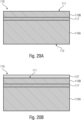
- An alternative bottom-up approach for creating the protruding upright nanostructures 150 will be described in the following with reference to Figures 20A to 20H .
- Figure 20E shows a method step, wherein upright nanostructures 150 are created at the first substrate surface 111, e.g., by growing.
- the upright nanostructures 150 can be grown inside the openings 125 provided in the material layer 121 (c.f. Figure 20D ).
- methods to bottom-up grow the silicon nanostructures 150 may include vapor-liquid-solid (VLS), solution-liquid-solid (SLS), and electrochemical methods.
- Figure 20F shows a further method step, wherein the material layer 121 is removed such that only the upright nanostructures 150 may remain on the first substrate surface 111.
- Figures 17A to 17F and Figures 18A to 18F showed method steps for creating a membrane structure 130 with protruding nanostructures 150 that faced away from the cavity 116, respectively.
- Figures 19A to 19J and Figures 20A to 20H showed method steps for creating a membrane structure 130 with protruding nanostructures 150 that faced the cavity 116, respectively.
- the nanostructures 150 may be created in the first substrate surface 111 by structuring / patterning the substrate 110.
- the substrate 110 may be structured / patterned by using photolithography or laser structuring.
- the nanostructures 150 may be configured as so-called laser induced periodical structures (LIPSS) which may be created by femtosecond lasers.
- LIPSS laser induced periodical structures
- DLIP direct laser interference patterning
- DLW direct laser writing
- the protruding upright nanostructures 150 may be configured as three-dimensional structures, as exemplarily discussed above with reference to Figures 4 , 5 and 6 .
- one of the core solutions of the herein described innovative concept is the provision of a nanostructured membrane and its applications on MEMS devices 100, like MEMS microphones and environmental barriers.
- the integrated nanostructures 150 can result in (super)hydrophobic or omniphobic surface characteristics to repel incoming liquid droplets.
- Parts of this disclosure concern design/concept and fabrication processes of upright (e.g., vertical) nanostructure arrays on membranes 130 of MEMS microphones and environmental barriers.
- MEMS microphones and environmental barriers with integrated upright nanostructure arrays yield (super)omniphobic membrane surfaces.
- a MEMS microphone with a superomniphobic nanostructure array-integrated membrane comprises a high environmental robustness.
- the present innovative concept allows to provide MEMS microphones with integrated nanostructures 150 either directly on the MEMS membrane 130 or on a discrete environmental barrier.
- the common approach to increase the environmental robustness of MEMS microphones is by integrating external environmental barriers made of polymer having hydrophobic and oleophobic characteristics into the package.
- the environmental barrier covering the sound port is located either inside (directly underneath the MEMS microphone) or outside the metal package lid (embedded on the structured printed circuit board (PCB)).
- PCB structured printed circuit board
- SAMs deposited on planar silicon surface might also result in hydrophobic characteristics.
- organic materials are known to degrade within device operation time.
- the present concept combines physical and chemical methods into one (i.e., SAM/Si nanopillars) to reach higher environmental robustness.
- a MEMS - microelectromechanical system - device comprising a substrate (110) comprising a vertically extending through hole (120) (wherein the vertically extending through hole corresponds to the above discussed cavity 116) and a horizontally extending membrane structure (130) covering the through hole (120), wherein the membrane structure (130) may comprise a plurality of protruding and/or upright nanostructures (150) for providing a liquid repellent membrane surface.
- the upright / protruding nanostructures (150) may be configured as three-dimensional geometric structures extending from the membrane structure (130), and extending into a direction away from the membrane structure (130).
- the upright / protruding nanostructures (150) may comprise at least one of:
- the plurality of upright / protruding nanostructures (150) provided on the membrane structure (130) may provide a membrane surface comprising at least one of a hydrophobic and an oleophobic surface characteristic.
- the upright / protruding nanostructures (150) may comprise at least one of the following geometrical shapes:
- the upright / protruding nanostructures (150) may be coated with an organic Self Assembled Monolayer - SAM -.
- the upright / protruding nanostructures (150) may comprise inorganic nanodots (190) or nanowires (190) extending from an outer surface of the upright / protruding nanostructures (150).
- the horizontally extending membrane structure (130) may comprise a first membrane surface (130A) facing the through hole (120) and an opposite second membrane surface (130B) facing away from the through hole (120), and the upright / protruding nanostructures (150) may be arranged on at least one of the first and second membrane surfaces (130A, 130B).
- the MEMS device (100) may be configured as a MEMS microphone, in which the horizontally extending membrane structure (130) may be configured as a microphone sound transducer membrane, wherein the upright / protruding nanostructures (150) may be arranged at the microphone sound transducer membrane.
- the MEMS device (100) may further comprise a MEMS microphone (300) comprising a microphone sound transducer membrane (310), wherein the MEMS device (100) may be configured as an environmental barrier structure comprising an environmental barrier membrane or mesh structure for protecting the microphone sound transducer membrane (310) from moisture and/or environmental particles, and wherein the horizontally extending membrane structure (130), at which the upright / protruding nanostructures (150) are arranged, may be configured as the environmental barrier membrane or mesh structure.
- the MEMS microphone may comprise a sound port (211) through which acoustic waves reach the membrane structure (130), wherein the membrane structure (130) may be positioned such that the upright / protruding nanostructures (150) face the sound port (211).
- the plurality of upright / protruding nanostructures (150) may comprise an area density of 10 6 - 10 10 nanostructures per cm 2 .
- a method for fabricating a MEMS device (100) comprising a step of providing a substrate (110) comprising a first substrate surface (111) and an opposite second substrate surface (112), wherein the substrate (110) comprises a sacrificial layer (140) arranged at the first substrate surface (111), and a step of structuring nanoimprints (113) into the sacrificial layer (140), and a step of filling the nanoimprints (113) by depositing a first material (114) onto the structured sacrificial layer (140), and a step of structuring a cavity (116) into the substrate (110), the cavity (116) being positioned opposite to the filled nanoimprints (113) and extending between the second substrate surface (112) and the sacrificial layer (140), and a step of releasing the filled nanoimprints (113) by removing the sacrificial layer (140) through the cavity (116), thereby creating a horizontally extending membrane structure (
- the horizontally extending membrane (130) and the upright / protruding nanostructures (150) may be made from the deposited first material (114).
- the method may further comprise steps of removing the deposited first material (114) from the sacrificial layer (140) while maintaining the deposited first material (114) inside the filled nanoimprints (113), and depositing a different second material (124) onto the sacrificial layer (140) and the filled nanoimprints (113), such that the horizontally extending membrane (130) is made from the deposited second material (124) while the upright / protruding nanostructures (150) are made from the first material (114).
- a method for fabricating a MEMS device (100) comprising a step of providing a substrate (110) having a first substrate surface (111) and an opposite second substrate surface (112), and a step of creating upright / protruding nanostructures (150) in the first substrate surface (111), and a step of structuring a cavity (116) into the substrate (110), the cavity (116) being positioned opposite to the upright / protruding nanostructures (150), and the cavity (116) extending from the second substrate surface (112) up to a remaining substrate portion (110C) between the cavity (116) and the upright / protruding nanostructures (150), thereby creating a membrane structure (130) horizontally extending over the cavity (116) and having the upright / protruding nanostructures (150) integrated therein, wherein the upright / protruding nanostructures (150) face away from the cavity (116).
- the step of creating the upright / protruding nanostructures (150) in the first substrate surface (111) may comprises at least one of the following steps:
- the method may further comprise a step of applying a coating onto the upright / protruding nanostructures (150), the coating comprising an organic self-assembled monolayer.
- the method may further comprise a step of depositing a film of inorganic material onto the upright / protruding nanostructures (150) for forming inorganic nanoseeds, and a step of growing nanowires (190) from the deposited nanoseeds, such that the grown nanowires (190) extend from an outer surface of the upright / protruding nanostructures (150).
- aspects have been described in the context of an apparatus, it is clear that these aspects also represent a description of the corresponding method, where a block or device corresponds to a method step or a feature of a method step. Analogously, aspects described in the context of a method step also represent a description of a corresponding block or item or feature of a corresponding apparatus.
Landscapes
- Engineering & Computer Science (AREA)
- Microelectronics & Electronic Packaging (AREA)
- Manufacturing & Machinery (AREA)
- Computer Hardware Design (AREA)
- General Health & Medical Sciences (AREA)
- Health & Medical Sciences (AREA)
- Toxicology (AREA)
- Physics & Mathematics (AREA)
- Chemical & Material Sciences (AREA)
- Signal Processing (AREA)
- Acoustics & Sound (AREA)
- Nanotechnology (AREA)
- Analytical Chemistry (AREA)
- Molecular Biology (AREA)
- Life Sciences & Earth Sciences (AREA)
- Condensed Matter Physics & Semiconductors (AREA)
- General Physics & Mathematics (AREA)
- Crystallography & Structural Chemistry (AREA)
- Micromachines (AREA)
Abstract
This disclosure concerns a method for producing a MEMS device (100), the method comprising a step of providing a substrate (110) comprising a first substrate surface (111) and an opposite second substrate surface (112), wherein the substrate (110) comprises a sacrificial layer (140) arranged at the first substrate surface (111), and a step of depositing a membrane material layer (114) onto the sacrificial layer (140). The membrane material layer (114) forms a free-standing membrane structure (130). The method further comprises a step of creating nanostructures (150) protruding from the membrane material layer (114), wherein the nanostructures (150) are created by applying a laser structuring process.
Description
- Embodiments of the present disclosure relate to a method for producing MEMS device (MEMS: microelectromechanical system) comprising a membrane with a liquid repellent membrane surface, wherein the membrane has at least one of oleophobic and hydrophobic characteristics.
- MEMS-based systems are miniaturized systems that comprise a very small form factor. For example, pressure transducers may be provided as MEMS devices, wherein a small membrane may transduce mechanical oscillations of the membrane into electric signals, or vice versa. An example of a MEMS pressure transducer may be a tire pressure sensor that monitors air pressure in tires. A further example may be a MEMS microphone that transduces sound waves (as an example of air pressure), such as music or voice, into electric signals, which can then be converted into digital data. In the reverse direction, a MEMS speaker may convert digital data into sound by oscillating the membrane.
- Due to their miniaturized size, MEMS pressure transducers require environmental protection because they can be influenced by several environmental ingress from the surrounding environment, for instance dust particles, water and moisture, which can then lead to lower robustness level and shorter operation time.
- For example, currently available MEMS-based microphones often have failures when they are exposed to liquids, for example water droplets, salt-containing liquids, sweat or oil. In case water droplets containing conductive particles, such as salts, reach the MEMS microphone membrane via the bottom sound port, these particles can remain on the bottom membrane surface when the water has evaporated, which may often result in device contamination, corrosion and/or electrical shortcut (leakage). If this phenomenon occurs over a long time, the device may not work as it should, leading to lower robustness and shorter lifetime.
- The bottom membranes of MEMS microphones typically possess planar surfaces comprising hydrophilic characteristic, which is typical for planar silicon surfaces. Thus, droplets of water or other liquids tend to adsorb onto the membrane surface. After the liquids have evaporated, solid materials (e.g., salts, particles, and other contaminants) that were contained in said evaporated liquids may remain on the membrane.
- The commonly implemented solution to protect the membranes of MEMS microphones is by adding external discrete environmental barrier (EB) components, e.g., an EB membrane having hydrophobic / oleophobic characteristics, and which is placed either inside or outside the package lid covering the sound port. This solution has, however, some drawbacks, such as high production cost, large package size, low acoustic performance, and limited usage for applications.
- Therefore, it would be desirable to provide a MEMS device with a membrane comprising a liquid repellent membrane surface and an inherent oleophobic and/or hydrophobic characteristic without the above mentioned drawbacks.
- This can be achieved by means of the herein disclosed MEMS device and the corresponding method for fabricating the MEMS device according to the independent claims. Further embodiments and advantageous aspects are suggested in the dependent claims.
- One aspect concerns a method for producing a MEMS device, the method comprising a step of providing a substrate comprising a first substrate surface and an opposite second substrate surface, wherein the substrate comprises a sacrificial layer arranged at the first substrate surface. The method further comprises a step of depositing a membrane material layer onto the sacrificial layer, and a step of structuring a cavity into the substrate, the cavity extending between the second substrate surface and the sacrificial layer. The method further comprises a step of releasing the membrane material layer by removing the sacrificial layer from the cavity such that the cavity is adjacent to the membrane material layer, wherein the released membrane material layer forms a free-standing membrane structure covering the cavity. The method further comprises a step of creating nanostructures in at least one of the first and second surfaces of the membrane material layer, wherein the nanostructures protrude from the respective surface of the membrane material layer, wherein the nanostructures are created by applying a laser structuring process.
- A further aspect concerns a MEMS - microelectromechanical system - device comprising a substrate having a cavity formed therein, the cavity extending vertically through the substrate, and a membrane material layer being attached to the substrate, said membrane material layer forming a horizontally extending free-standing membrane structure covering the cavity. The membrane material layer comprises a plurality of nanostructures for providing a liquid repellent membrane surface, wherein the nanostructures protrude from at least one of two opposing surfaces of the membrane material layer. The nanostructures are created by laser structuring such that they are monolithically integrated in the membrane material layer.
- In the following, embodiments of the present disclosure are described in more detail with reference to the figures, in which
- Fig. 1A
- shows a schematic cut perspective view of a MEMS device according to an embodiment being configured as a discrete environmental barrier,
- Fig. 1B
- shows a schematic side view of the MEMS device of
Figure 1A , - Fig. 2A
- shows a schematic cut perspective view of a MEMS device according to an embodiment being configured as a MEMS-based single backplate microphone,
- Fig. 2B
- shows a schematic side view of the MEMS device of
Figure 2A , - Fig. 3A
- shows a schematic cut perspective view of a MEMS device according to an embodiment being configured as a MEMS-based sealed dual-membrane microphone,
- Fig. 3B
- shows a schematic side view of the MEMS device of
Figure 3A , - Fig. 4
- shows a schematic perspective view of upright three-dimensional nanostructures to be used in combination with a membrane structure according to an embodiment,
- Fig. 5
- shows a schematic perspective view of some further upright three-dimensional nanostructures to be used in combination with a membrane structure according to an embodiment,
- Fig. 6
- shows a schematic perspective view of some further upright three-dimensional nanostructures to be used in combination with a membrane structure according to an embodiment,
- Figs. 7A-7E
- show schematic side views of different geometrical shapes of upright nanostructures to be used in combination with a membrane structure according to different embodiments,
- Fig. 8
- shows a schematic side view of upright three-dimensional nanostructures being coated with an organic self-assembled monolayer according to an embodiment,
- Fig. 9
- shows a schematic side view of upright three-dimensional nanostructures being decorated with nanowires according to an embodiment,
- Fig. 10A
- shows a schematic side view of a MEMS-based package according to an embodiment, wherein the package comprises a MEMS device according to an embodiment, the MEMS device being configured as a MEMS-based single backplate microphone,
- Fig. 10B
- shows a schematic side view of a MEMS-based package according to an embodiment, wherein the package comprises a MEMS device according to an embodiment, the MEMS device being configured as a MEMS-based sealed dual membrane microphone,
- Fig. 10C
- shows a schematic side view of a MEMS-based package according to an embodiment, wherein the package comprises a MEMS device according to an embodiment, the MEMS device being configured as a MEMS-based discrete environmental barrier,
- Figs. 11A-11F
- show method steps of a method for fabricating a MEMS device according to an embodiment, wherein the nanostructures are created in a first membrane surface by means of a laser structuring process,
- Fig. 12
- shows an embodiment, wherein the laser structured nanostructures are created in an opposite second membrane surface,
- Figs. 13A-13C
- show method steps of a method for fabricating a MEMS device according to an embodiment, wherein the nanostructures are created in the membrane material layer and in portions of the substrate by means of a laser structuring process,
- Figs. 14A-14B
- show method steps of a method for fabricating a MEMS device according to an embodiment, wherein the laser structured nanostructures are created in nanopillars being previously created by lithography,
- Figs. 15A-15C
- show enlarged sections of a membrane material layer comprising nanopillars being created by lithography, wherein the laser structured nanostructures are created in said nanopillars and gaps in between,
- Fig. 16
- shows a MEMS device comprising a membrane material layer with protruding laser structured nanostructures, wherein at least the membrane material layer is coated with a Self Assembled Monolayer (SAM),
- Figs. 17A-17F
- show method steps of a method for fabricating a MEMS device according to an embodiment, wherein the horizontally extending membrane structure and the upright nanostructures are made from the same material,
- Figs. 18A-18F
- show method steps of a method for fabricating a MEMS device according to an embodiment, wherein the horizontally extending membrane structure and the upright nanostructures are made from different materials,
- Figs. 19A-19J
- show method steps of a method for fabricating a MEMS device according to an embodiment, wherein the horizontally extending membrane structure and the upright nanostructures are directly structured into the substrate material, and
- Figs. 20A-20H
- show method steps of a method for fabricating a MEMS device according to an embodiment, wherein the horizontally extending membrane structure is directly structured into the substrate material and wherein the upright nanostructures are grown on the substrate material.
- Equal or equivalent elements or elements with equal or equivalent functionality are denoted in the following description by equal or equivalent reference numerals.
- Method steps which are depicted by means of a block diagram and which are described with reference to said block diagram may also be executed in an order different from the depicted and/or described order. Furthermore, method steps concerning a particular feature of a device may be replaceable with said feature of said device, and the other way around.
- In the following description, a MEMS-based microphone will be mentioned as a non-limiting example for a MEMS device. However, other MEMS devices with a membrane structure comprising a plurality of upright nanostructures also fall under the scope of protection according to the herein described innovative concept.
- Furthermore, terms like horizontally and vertically will be used in the following description. Of course, these terms are to be understood in relation to each other, but not necessarily in relation to the earth's horizon. Accordingly, the term horizontally may be synonymously used with "extending in a first direction / plane", while the term vertically may be synonymously used with "extending in a second direction / plane", the second direction / plane being perpendicular to the first direction / plane. For example, a substrate may comprise a primary extension direction, which may also be referred to as the substrate plane. For example, the term "horizontally" is to be understood as "parallel to the substrate plane" or "in plane", while the term "vertically" is to be understood as "perpendicular to the substrate plane".
- Furthermore, upright nanostructures may be described, wherein said upright nanostructures may be arranged on a membrane structure. The term "upright" means that the nanostructures may extend away from the membrane structure, for example in an upward direction. For example, if the membrane structure may extend horizontally, the nanostructures may extend substantially vertically from the membrane structure. Whenever the term "vertically extending" is used in the present disclosure, it is within the scope of the present disclosure that the nanostructures may not be perfectly vertical, but that the nanostructures may be slightly tilted. For example, the terms "upright" and "vertically extending" may include that the nanostructures may be skew and may extend away from the membrane structure in an angle of 90° ±25°. Furthermore, some embodiments refer to a plurality of nanostructures that may be arranged, for instance, in a nanostructure array. Accordingly, the present disclosure always refers to a majority (i.e. at least 50%) of the nanostructures. For example, if the present disclosure mentions that the nanostructures are upright, it means that at least 50% of the nanostructures are upright. In real life, it may be possible that several hundreds or thousands of nanostructures may be present, wherein most of them are upright, e.g., substantially vertical, while a few percent of them may not be upright (less than 75° or more than 115°). Furthermore, some embodiments may describe horizontally extending membrane structures as non-limiting examples for membrane structures in general. In such embodiments, vertically extending nanostructures may be described as non-limiting examples of upright nanostructures. Accordingly, the terms "vertically extending" and "upright" may be used synonymously in the present disclosure.
-
Figures 1A and 1B show a first embodiment of aMEMS device 100 according to the herein described innovative concept. TheMEMS device 100 comprises asubstrate 110. For example, thesubstrate 110 may comprise or be made from silicon. Thesubstrate 110 comprises a vertically extendingcavity 116 that may extend completely through thesubstrate 110. - The
MEMS device 100 further comprises a horizontally extendingmembrane structure 130. For example, themembrane structure 130 may comprise or be made from polysilicon. Themembrane structure 130 covers thecavity 116. As will be described in more detail below, themembrane structure 130 may be created from amembrane material layer 114 being deposited on a sacrificial layer 140 (e.g., TEOS: tetraethoxysilane or tetraethyl orthosilicate). Thesacrificial layer 140 may be sandwiched between thesubstrate 110 and themembrane material layer 114 and may connect themembrane structure 130 with thesubstrate 110. Alternatively, themembrane structure 130 may be adhered to thesubstrate 110, e.g., by means of an adhesive. - According to the present innovative concept, a plurality of upright (e.g., vertically extending)
nanostructures 150 is created in themembrane material layer 114 by applying a laser structuring process, such that thenanostructures 150 protrude from at least one of two opposingmembrane surface - In particular, the horizontally extending
membrane material layer 114 comprises afirst membrane surface 114A facing thecavity 116, and an oppositesecond membrane surface 114B facing away from thecavity 116. As exemplarily depicted inFigures 1A and 1B , the protrudingnanostructures 150 may be arranged on thefirst membrane surface 114A. Additionally or alternatively, the protrudingnanostructures 150 may be arranged on thesecond membrane surface 114B. This holds for each and every embodiment as discussed herein. - According to the herein disclosed innovative concept, the protruding
nanostructures 150 are created by applying a laser structuring process, as will be discussed in more detail later with reference toFigures 11A to 16 . Therefore, thenanostructures 150 may be monolithically integrated in themembrane material layer 114. Accordingly, themembrane material layer 114 forms a free-standingmembrane structure 130 with integratedprotruding nanostructures 150. - The protruding
nanostructures 150 may extend substantially perpendicular to themembrane structure 130. The protrudingnanostructures 150 provide for a self-cleaning surface characteristic exploiting the so-called lotus effect. Accordingly, the protrudingnanostructures 150 provide for a liquid repellent membrane surface of themembrane structure 130. In particular, the protrudingnanostructures 150 create a roughnanostructured membrane surface membrane structure 130. - In contrast, a membrane without these protruding
nanostructures 150 may comprise a hydrophilic surface characteristic, i.e., liquids (water, oil, etc.) adhere to the membrane. If the liquid evaporates, solid matters (like salts, particles, and other contaminants) that are solved in said liquids, may remain on the membrane surface which may often result in device contamination, corrosion and/or electrical shortcut (leakage). Themembrane structure 130 of the herein described innovative concept, instead, comprises a hydrophobic and/or oleophobic surface characteristic, i.e., liquids (water, oil, etc.) are repelled from themembrane structure 130. Said hydrophobic and/or oleophobic surface characteristics are provided by the protrudingnanostructures 150. - The
MEMS device 100 as depicted inFigures 1A and 1B may be configured as a discrete environmental barrier structure, e.g., an environmental barrier mesh or membrane. Suchenvironmental barrier structures 100 may be used in connection with MEMS microphones in order to protect the thin and fragile microphone membrane from ingress of environmental particles, moisture and other physical and/or chemical objects. Details will be discussed later with reference toFigures 10A to 10C . -
Figures 2A and 2B show a further embodiment of aMEMS device 100. In this non-limiting example, a so-called single backplate (SBP) MEMS-basedmicrophone 100 is shown. In addition to the embodiment discussed above with reference toFigures 1A and 1B , thesingle backplate microphone 100 comprises anelectrode structure 160 that can be electrically connected, e.g., by means of pads /terminals 170, to a circuitry (not shown). For example, theelectrode structure 160 may comprise or be made from silicon nitride, Si3N4. - The
membrane structure 130 may be configured as a microphone membrane that can oscillate in response to acoustic waves. The acoustic waves may enter the microphone package through a so-called sound port. The depictedsingle backplate microphone 100 may be mounted over the sound port, such that the acoustic waves may enter the vertically extendingcavity 116 and arrive at the bottom surface of themembrane structure 130. - As mentioned above, the upright (e.g., vertically extending)
nanostructures 150, which protrude from themembrane structure 130, may provide for a hydrophobic / oleophobic surface characteristic of themembrane structure 130. Thus, liquids contained in the air that is transferred by the acoustic waves may be repelled from the hydrophobic and/or oleophobic membrane surface. Accordingly, it is advantageous if the protrudingnanostructures 150 are provided at a membrane surface that faces a source of environmental liquids, for example the sound port. Thus, in this non-limiting example, the protrudingnanostructures 150 may face thecavity 116 and may vertically extend into thecavity 116. However, as will be explained below, the protrudingnanostructures 150 may additionally or alternatively face away from thecavity 116 and may vertically extend away from thecavity 116. In other words, the protrudingnanostructures 150 may be arranged on either one of the twomembrane surfaces membrane surfaces -
Figures 3A and 3B show a further embodiment of aMEMS device 100. In this non-limiting example, a so-called sealed dual-membrane (SDM) MEMS-basedmicrophone 100 is shown. In addition to the embodiments discussed above, the sealed dual-membrane microphone 100 comprises amembrane structure 130 having afirst membrane portion 131 and asecond membrane portion 132. Anelectrode structure 160 is sandwiched between the first andsecond membrane portions membrane portions electrode structure 160 may be a rigid electrode structure, such as a backplate or a stator, for example. - At least one of the first and
second membrane portions upright nanostructures 150 that protrude from therespective membrane portion nanostructures 150 are provided at a membrane surface that faces a source of environmental liquids, for example the sound port. Thus, in this non-limiting example, the protrudingnanostructures 150 may be arranged on thesecond membrane portion 132 facing thecavity 116. - The protruding
nanostructures 150 may be configured as upright (e.g., vertically extending) nanospikes, nanotubes, nanofins, nanopillars, nanowhiskers, nanowalls, nanocircular walls, black silicon, and many more, while various other geometric designs and shapes are possible. In any case, the protrudingnanostructures 150 may be configured as single, free-standing 3D elements, that protrude from a plane surface, e.g, from at least one of the two opposing membrane surfaces 114A, 114B of themembrane structure 130. The protrudingnanostructures 150 may not be connected to each other, i.e., they are configured as individual unconnected elements. This is a difference compared to meshes and grids, which may sometimes be used as environmental barrier structures. Meshes and grids comprise a plurality of single mesh segments / grid segments that are all connected to each other to form the mesh / grid structure. -
Figures 4 to 6 show some non-limiting examples of protrudingnanostructures 150 being configured as single free-standing and unconnected 3D elements.Figure 4 shows protruding nanostructures 150 being configured as single free-standing and unconnectedupright walls or plates being consecutively arranged along a (straight or curved) line.Figure 5 shows protruding nanostructures 150 being configured as single free-standing and unconnected concentric walls.Figure 6 shows protruding nanostructures 150 being configured as single free-standing and unconnected (hollow) nanotubes. - Summarizing in a more general terminology, the protruding
upright nanostructures 150 may be configured as single unconnected three-dimensional geometric structures extending away from themembrane structure 130. For example, the protrudingupright nanostructures 150 may extend into a direction that is substantially perpendicular to the lateral extension of themembrane structure 130. - For example, the single
unconnected nanostructures 150 may be configured as single upright nanopillars protruding and extending away from themembrane structure 130. Nanopillars are pillar-shaped nanostructures, approximately a few nanometers (e.g. 10 nm to 1.000 nm) in diameter, that can be grouped together in lattice like arrays. In such an array configuration, the protrudingnanostructures 150 may be densely arranged next to each other. According to an embodiment, the plurality of protrudingnanostructures 150 may comprise an area density of 106 - 1010 nanostructures per cm2. - In some embodiments, the protruding
nanostructures 150 may comprise a geometrical shape similar to a frustum cone. However, various other geometrical shapes are possible, as exemplarily depicted inFigures 7A to 7E . As shown inFigure 7A , theupright nanostructures 150 may comprise a geometrical shape similar to a straight cylinder protruding from themembrane structure 130. As shown inFigure 7B , theupright nanostructures 150 may comprise a geometrical shape similar to a frustum cone protruding from themembrane structure 130. As shown inFigure 7C , theupright nanostructures 150 may comprise a geometrical shape similar to an inverted frustum cone protruding from themembrane structure 130. As shown inFigure 7D , theupright nanostructures 150 may comprise a T-shape, i.e., a geometrical shape similar to the letter 'T', and they may protrude from themembrane structure 130. As shown inFigure 7E , theupright nanostructures 150 may comprise a multifaceted T-shape, i.e., a geometrical shape similar to the letter 'T' with additional contoured walls (e.g., reentrant structure), and they may protrude from themembrane structure 130. The different geometrical shapes may lead to different hydrophobic and/or oleophobic surface characteristics of the protrudingnanostructures 150. - Besides different geometrical shapes, further advanced surface chemistry modification can be realized by introducing organic self-assembled monolayers, so-called SAMs. For example,
Figure 8 shows an embodiment, wherein the protrudingnanostructures 150 may be coated with organic self-assembled monolayers.Nanostructures 150 being coated with SAMs exhibit an enhanced level of hydrophobicity and/or oleophobicity compared touncoated nanostructures 150. Using this combined chemical/physical method, the SAM-coatednanostructures 150 can increase the resulting water or liquid contact angle on their surface and can repel not only water but also other liquids (e.g., oil) resulting in (super-)hydrophobic or omniphobic surfaces. - Different self-assembled monolayers, and in particular silane-based SAMs, may be used for coating the protruding
nanostructures 150. For example, the organic self-assembled monolayers may comprise, or may consist of, at least one of: - Fluoroalkylsilanes (FAS),
- Perfluorodecyltrichlorosilane (FDTS),
- Heptadecafluoro-1,1,2,2-tetrahydrodecyltrichlorosilane (HDFS),
- Tridecafluoro-1,1,2,2-tetrahydrooctyltrichlorosilane (FOTS),
- Octadecyltrichlorsilane (ODTS),
- Methyltrimethoxysilane (MTMS),
- Bis(trimethylsilyl)amine or hexamethyldisilazane (HMDS),
- (3-Aminopropyl)triethoxysilane (APTES),
- Dichlorodimethylsilane (DDMS),
- Octadecyltrimethoxysilane (OTMS),
- Ethyltriethoxysilane (ETES), and
- 1H,1H,2H,2H-perfluorooctyltriethoxysilane (HFOTES).
-
Figure 9 shows a further embodiment, wherein the protrudingnanostructures 150 may comprise inorganic nano-elements 190, e.g., nanodots or nanowires, protruding from a surface of thenanostructures 150.Nanostructures 150 comprising additional nano-elements 190 exhibit an enhanced level of hydrophobicity and/or oleophobicity compared to bare/naked nanostructures 150. - The inorganic nano-
elements 190 may be grown on the surface of thenanostructures 150. For example, a suitable material, for example zinc oxide (ZnO), may be used for creating the nano-elements 190. For example, for creating ZnO nanowires, a zinc oxide film may be deposited onto the surface of thenanostructures 150 using e.g., a sputtering technique for forming ZnO nanoseeds. The growth of the ZnO nanowires can then be realized by employing e.g., a chemical bath deposition (CBD) process. Other alternative methods (e.g., hydrothermal method, vapor-liquid-solid process, spray pyrolysis, chemical vapor deposition, molecular beam epitaxy, electrodeposition, atomic layer deposition, and pulsed laser deposition) can also be opted to grow or deposit ZnO layer and create ZnO nanostructures. This combination with ZnO nanowires is beneficial for the case of coarse nanostructures 150 (e.g. nanostructures 150 with large pitch or distance among them). ZnO nano-elements 190 may be advantageously grown on silicon-basednanostructures 150. - In result, the grown nano-
elements 190 may protrude from thenanostructures 150, and they may extend substantially perpendicular from the surface of thenanostructures 150. Accordingly, thenanostructures 150 may comprise a tree-like shape. Each of the tree-like nanostructures 150 may comprise a plurality of inorganic nano-elements 190, e.g., nanowires. - As mentioned above, the
nanostructures 150 may provide for a hydrophobic and/or oleophobic and/or superhydrophobic and/or omniphobic surface characteristic of themembrane structure 130. To explain these surface characteristics, imagine an untreated planar silicon surface on which a water droplet is applied. Planar silicon surfaces in general comprise a hydrophilic surface characteristic, i.e., liquids are adhered to the planar surface due to its low surface roughness and, thus, its large surface energy. A hydrophilic surface comprises a small water contact angle. For example, the water contact angle may be around 5° to 20°. - In turn, a nanostructured silicon surface, for example the herein described rough nanostructured membrane surfaces 114A, 114B of the
membrane structure 130 with the protrudingnanostructures 150, may comprise a larger water contact angle of at least 120° or at least 150°. Therefore, a water droplet being applied to thenanostructured membrane surface nanostructures 150. Accordingly, themembrane structure 130 comprising the protrudingnanostructures 150 may comprise a hydrophobic or even superhydrophobic surface characteristic. - Superhydrophobic surfaces generally show water contact angles of greater than 150° (nearly perfect sphere) along with low contact angle hysteresis. Contact angle hysteresis is defined as the difference between measured values of the advancing and receding contact angles (the highest and lowest contact angles on such a structures).
- Additionally or alternatively, the
nanostructures 150 protruding from themembrane structure 130 may provide an oleophobic surface characteristic such that oils are repelled from the membrane surface, or even an omniphobic surface characteristic such that almost each and every liquid is repelled from the membrane surface. - Liquids that approach the
nanostructured membrane 130 having superhydrophobic/omniphobic surface characteristics will bounce or roll off. Hence, the herein discussednanostructures 150 are useful for water/liquid repellent and self-cleaning surfaces. The nanostructured membrane surface can be self-cleaning because any water/liquid droplets that contact it will roll off picking up any particles along with the operation of the movingmembrane 130. - By adjusting the geometry (e.g., diameter, height, aspect ratio, pitch) of the
nanostructures 150, the hydrophobicity / oleophobicity / omniphobicity level of thenanostructures 150 can be varied. - According to some embodiments, the protruding
nanostructures 150 may comprise a diameter of 1 µm or less. If thenanostructures 150 may comprise a varying diameter, e.g., if they were configured as frustum cones, the diameter is measured at the thickest portion. Additionally or alternatively, the protrudingnanostructures 150 may comprise a pitch, i.e., a distance between the centers of twoadjacent nanostructures 150, said pitch comprising a ratio of at least pitch : diameter = 2:1. Additionally or alternatively, the protrudingnanostructures 150 may comprise an aspect ratio (width-to-height) between 1:3 and 1:40. The authors of this disclosure have found thatnanostructures 150 with high aspect ratio (e.g., x > 5) produce a larger contact angle (more hydrophobicity / omniphobicity) than those with low aspect ratio (e.g., 1 < x < 5). - As mentioned above with reference to
Figures 1A to 3B , theMEMS device 100 may be configured as a MEMS-based microphone or as a discrete MEMS-based environmental barrier. TheMEMS device 100 may be housed underneath a lid so as to produce a MEMS-based package, e.g., a microphone package. -
Figure 10A shows a first embodiment of a MEMS-basedpackage 200. Thepackage 200 may comprise acomponent board 210, e.g., a printed circuit board (PCB). AMEMS device 100 according to the herein described innovative concept may be arranged on thecomponent board 210. Acircuitry 220 for controlling theMEMS device 100 may be arranged adjacent to theMEMS device 100. TheMEMS device 100 may be electrically connected to thecircuitry 220, for example by means of abond wire 230. - The
package 200 may further comprise alid 240 being arranged on thecomponent board 210. Thelid 240 may cover theMEMS device 100 and thecircuitry 220. The free space orcavity 250 underneath thehollow lid 240 may provide for an acoustic back volume. - The
component board 210 may comprise a vertically extending throughhole 211. In case the MEMS-basedpackage 200 is a microphone package (as exemplarily depicted here), the throughhole 211 may be referred to as a sound port through which acoustic waves may enter thecavity 250. - In this non-limiting example, the
MEMS device 100 may be configured as a MEMS-based single backplate (SBP) microphone, as previously discussed above with reference toFigures 2A and 2B . Here, the horizontally extendingmembrane structure 130 may be configured as a microphone sound transducer membrane, wherein theupright nanostructures 150 protrude from the microphonesound transducer membrane 130. In this example, the protrudingnanostructures 150 may be arranged on thefirst membrane surface 114A facing the through hole (sound port) 211. However, additionally or alternatively, the protrudingnanostructures 150 may be arranged on the oppositesecond membrane surface 114B facing away from the through hole (sound port) 211. For any further details as to the single components belonging to saidSBP microphone 100, it is referred to the discussion above. - As can be seen in
Figure 10A , theSBP microphone 100 is arranged directly opposite to thesound port 211, e.g., above thesound port 211. TheSBP microphone 100 is arranged such that it covers thesound port 211. When viewed from above, the horizontally extendingmembrane structure 130 circumferentially covers thesound port 211. In this non-limiting example, the protrudingnanostructures 150 face thesound port 211. - As mentioned above, acoustic waves may enter the
package 200 through thesound port 211. Since thesound port 211 is in fluid connection with thecavity 116, the acoustic waves may be further conveyed into thecavity 116 until reaching themembrane structure 130. Themembrane structure 130 will be deflected in response to the impinging acoustic waves. The amplitude of deflection will be measured by theelectrode structure 160. - The air through which the acoustic waves may travel may comprise moisture, e.g., liquids containing salt particles and the like. Since the herein described
innovative membrane structure 130 comprises the protrudingnanostructures 150, themembrane structure 130 shows a (super-)hydrophobic / omniphobic surface characteristic. Thus, intruding liquids and or any solid matter (like salts, particles, and other contaminants) contained in said liquids may be repelled from the surface of themembrane structure 130. This provides for a superior protection of themicrophone membrane 130. -
Figure 10B shows a further embodiment of a MEMS-basedpackage 200 being configured as a microphone package. Like elements with like features, as discussed with reference toFigure 10A , are indicated with same reference numerals. Accordingly, for further details it is referred to the above discussion. A difference compared to the above discussed embodiment (c.f.Figure 10A ) is the type ofMEMS device 100 used. In this non-limiting example, theMEMS device 100 is configured as a sealed dual-membrane (SDM) MEMS-based microphone. Regarding technical details of theSDM microphone 100 it is referred toFigures 3A and 3B . -
Figure 10C shows a further embodiment of a MEMS-basedpackage 200. Again, like elements with like features, as discussed with reference toFigures 10A and10B , are indicated with same reference numerals. In this non-limiting example, theMEMS device 100 according to the herein described innovative principle may be configured as a discrete MEMS-based environmental barrier structure. For details as to any elements comprised by saidenvironmental barrier 100, it is referred toFigures 1A and 1B above. - Furthermore, a MEMS-based
microphone 300 is depicted. This MEMS-basedmicrophone 300 may be aMEMS device 100 as discussed above, or a conventional MEMS-based microphone. In this non-limiting example, a conventional SDM microphone is depicted. However, it may also be possible that a SBP microphone may be used instead. The MEMS-basedmicrophone 300 may comprise a microphonesound transducer membrane 310. - As can be seen in
Figure 10C , theinnovative MEMS device 100 may be arranged between thesound port 211 and the MEMS-basedmicrophone 300. Thus, theMEMS device 100 being configured as an environmental barrier structure acts as an environmental barrier for protecting the MEMS microphonesound transducer membrane 310 from moisture and/or environmental particles. - The
MEMS device 100 being configured as an environmental barrier structure comprises a horizontally extending environmental barrier membrane or mesh structure. In this non-limiting example, theinnovative membrane structure 130 may be configured as the aforementioned environmental barrier membrane or mesh structure. - The
membrane structure 130 may comprise the protrudingnanostructures 150 as discussed herein. This provides for an improved hydrophobicity / omniphobicity level of themembrane structure 130. Thus, intruding liquids and or any solid matter (like salts, particles, and other contaminants) contained in said liquids may be repelled from the surface of themembrane structure 130. This provides for a superior protection of the downstream arrangedmicrophone membrane 310. - In the previous sections, different embodiments of the
MEMS device 100 were described. In the following, examples and embodiments of methods for manufacturing aMEMS device 100 will be discussed. -
Figures 11A to 11F show an embodiment of a method for fabricating aMEMS device 100 as discussed herein. According to the herein discussed innovative principle, the above discussed protrudingnanostructures 150 are created by applying a laser structuring process, as will be described in more detail below. -
Figure 11A shows a first method step, wherein asubstrate 110 is provided, thesubstrate 110 comprising afirst substrate surface 111 and an oppositesecond substrate surface 112. Thesubstrate 110 may comprise or consist of silicon. -
Figure 11B shows a further method step, wherein asacrificial layer 140 is arranged at thefirst substrate surface 111. Thesacrificial layer 140 may comprise or consist of tetraethoxysilane (TEOS). Alternatively, thesacrificial layer 140 may comprise or consist of one or more oxides. -
Figure 11C shows a further method step, wherein amembrane material layer 114 is deposited onto thesacrificial layer 140. Amembrane material layer 114 may comprise or be made from one or more materials that are suitable for providing a MEMS-membrane, e.g., polysilicon. -
Figure 11D shows a further method step, wherein acavity 116 is structured into thesubstrate 110. Thecavity 116 may be created by applying a suitable etching process, such as RIE or DRIE etching. Thecavity 116 may extend between thesecond substrate surface 112 and thesacrificial layer 140. Thecavity 116 may have the shape of a through hole that extends completely through thesubstrate 110 between the first and second substrate surfaces 111, 112. -
Figure 11E shows a further method step, wherein themembrane material layer 114 is released by removing thesacrificial layer 140 from thecavity 116, i.e. portions of thesacrificial layer 140 that were previously sitting inside the cavity (c.f.Figure 11D ) are removed, such that only residual portions of thesacrificial layer 140 may remain between substrate portions and themembrane material layer 114. Thesacrificial layer 140 may be removed by applying a suitable etching process, such as a chemical wet etching process. After removing the above mentioned portions of thesacrificial layer 140, thecavity 116 is directly adjacent to themembrane material layer 114. Accordingly, the releasedmembrane material layer 114 forms a free-standingmembrane structure 130 covering thecavity 116. -
Figure 11F shows a further method step, whereinnanostructures 150 are created in at least one of the first and second membrane surfaces 114A, 114B of themembrane material layer 114. According to the present innovative concept, thenanostructures 150 are created by applying a laser structuring process, wherein laser beams are schematically represented byarrows 180. The laser structuring can be applied prior to or after the step of releasing the membrane layer 114 (Fig. 11E ). - The applied laser structuring process may use a femto second laser or a pico second laser. This may have the advantage that membrane material may change from solid to gas, without an intermediate liquid state, and heat input may be limited to specific spots. Thus, the
nanostructures 150 may be formed from themembrane material layer 114, or in other words, thenanostructures 150 may be monolithically integrated in themembrane material layer 114. - Accordingly, the step of creating the
nanostructures 150 may comprise a step of removingportions 118 of themembrane material layer 114 by means of one ormore laser beams 180 being used in the applied laser structuring process, wherein thenanostructures 150 remain between the removedportions 118 of themembrane material layer 114, such that thenanostructures 150 are monolithically integrated in themembrane material layer 114. - Additionally or alternatively, the applied laser structuring process may comprise Direct Laser Interference Patterning (DLIP), wherein interference patterns may be directly imprinted into the
membrane surface membrane material layer 114. Thereby, a plurality ofnanostructures 150 may be created with a single laser beam. - The step of creating the
nanostructures 150 may comprise distributing thenanostructures 150 in a random or periodic pattern along therespective membrane surface membrane material layer 114. - The
nanostructures 150 that are created according to the herein described innovative principle are not only monolithically integrated in themembrane material layer 114, but they also protrude from therespective membrane surface membrane material layer 114. Thus, the protrudingnanostructures 150 provide for an increased surface roughness (compared to unstructured plane membrane surfaces without nanostructures) of therespective membrane surface membrane material layer 114 and, thus, of themembrane structure 130 created therefrom. - In the non-limiting example shown in
Figure 11F , thenanostructures 150 are created in thefirst membrane surface 114A of themembrane material layer 114, saidfirst membrane surface 114A facing thecavity 116, such that thenanostructures 150 also face thecavity 116. In this case, the one ormore laser beams 180 is/are guided into thecavity 116 so as to reach thefirst membrane surface 114A of themembrane material layer 114 through thecavity 116. This may be performed as a last process step in the frontend production leading to a simplified processing of creating the protrudingnanostructures 150 compared to other processes, such as lithography processes. -
Figure 12 shows an alternative method step, wherein the protrudingnanostructures 150 are created in thesecond membrane surface 114B, saidsecond membrane surface 114B facing away from thecavity 116, such that thenanostructures 150 also face away from thecavity 116. In this case, the one ormore laser beams 180 is/are guided over thesecond membrane surface 114B of themembrane material layer 114. - As a further alternative, which is not explicitly depicted here, the protruding
nanostructures 150 may be created in the first and second membrane surfaces 114A, 114B. -
Figure 13A shows an optional method step, wherein the one ormore laser beams 180 being used in the applied laser structuring process is/are guided over an exposedportion 112A of thesecond substrate surface 112 that remains after creating thecavity 116. Accordingly, the remaining exposedportion 112A is located outside thecavity 116, such thatadditional nanostructures 151 are created in said exposedportions 112A of thesecond substrate surface 112. In this case, theadditional nanostructures 151 may be formed integrally / monolithically with the laser-treatedexposed portions 112A of thesecond substrate surface 112. Furthermore, theadditional nanostructures 151 may protrude from the laser-treatedexposed portions 112A of thesecond substrate surface 112 thereby increasing their surface roughness leading to an increased hydrophobicity / olephobicity. -
Figure 13B shows a further optional method step, wherein the one ormore laser beams 180 being used in the applied laser structuring process is/are guided over one or moreinner substrate portions 110A (e.g., inner side walls) residing inside thecavity 116, such thatadditional nanostructures 152 are created in said one or moreinner substrate portions 110A. In this case, theadditional nanostructures 152 may be formed integrally / monolithically with the laser-treatedinner substrate portions 110A. Furthermore, theadditional nanostructures 152 may protrude from the laser-treatedinner substrate portions 110A thereby increasing their surface roughness leading to an increased hydrophobicity / olephobicity. -
Figure 13C shows a further alternative, wherein the additionalprotruding nanostructures portions 112A of thesecond substrate surface 112 and in theinner substrate portions 110A residing inside thecavity 116. -
Figures 14A and 14B show a further embodiment of a method for producing the above discussedinnovative MEMS device 100. This method is a combined method in which lithography is combined with laser structuring. In particular, prior to the step of creating thenanostructures 150 by applying the laser structuring process, the method comprises a step of creatingnanopillars 155 in at least one of the first and second membrane surfaces 114A, 114B of themembrane material layer 114 by applying a lithography and etching process, wherein saidnanopillars 155 protrude from therespective membrane surface membrane material layer 114. In the example shown inFigure 14A , thenanopillars 155 being created by lithography are formed in thefirst membrane surface 114A. - As shown in
Figure 14B , thenanostructures 150 are then created in saidnanopillars 155 by applying the above discussed laser structuring process, wherein the laser beams are schematically depicted by means ofarrows 180. In this example, the laser structurednanostructures 150 are created in atop surface 156 of thenanopillars 155, wherein saidtop surface 156 faces away from themembrane material layer 114, i.e. it faces thecavity 116. In result, the laser structurednanostructures 150 protrude from thenanopillars 155 created in themembrane material layer 114 by means of lithography and, as such, thenanostructures 150 protrude from themembrane material layer 114. - The
nanopillars 155 created by lithography may comprise an average diameter that is at least ten times larger than an average diameter of the laser structurednanostructures 150. For example, thenanopillars 155 may comprise a diameter of 100 nm, and the laser structurednanostructures 150 may comprise a diameter of 10 nm. -
Figures 15A to 15C show some non-limiting examples of laser structurednanostructures 150 and how they can be structured into thenanopillars 155 by applying the laser structuring process.Figure 15A shows a first example that corresponds to the embodiment described above with reference toFigure 14B . Here, the laser structurednanostructures 150 are created in thetop surface 156 of thenanopillars 155. -
Figure 15B shows a further example, wherein the laser structurednanostructures 150 comprise different sizes. For example, the laser structurednanostructures 150 may comprise different diameters. Accordingly, the laser structurednanostructures 150 may be arranged more or less densely among each other. This may apply to each and every embodiment discussed herein. -
Figure 15C shows a further example, wherein the step of creating thenanostructures 150 by applying the laser structuring process comprises a step of creating thenanostructures 150 in arecess 157 between twoadjacent nanopillars 155. As exemplarily depicted inFigure 15C , the laser structurednanostructures 150 may be created inside therecess 157 in addition to the creation of laser structurednanostructures 150 in thetop surfaces 156 of thenanopillars 155. Alternatively, but not explicitly depicted here, the laser structurednanostructures 150 may be created inside a recess 157only, i.e. without any laser structurednanostructures 150 being provided in thetop surfaces 156 of thenanopillars 155. - The
nanopillars 155 may also be referred to as nanowhiskers. In some embodiments, the above discussednanopillars 155 may comprise a geometrical shape that is different to a pillar. However, for the sake of easy differentiation from the laser structurednanostructures 150, they may generally be referred to asnanopillars 155 within this disclosure. Furthermore, while thenanopillars 155 have been described as being created by means of lithography, other embodiments may include that thenanopillars 155 are created differently, for example also by means of laser structuring, or thenanopillars 155 may be deposited onto at least one of the membrane surfaces 114A, 114B. -
Figure 16 shows a further embodiment of the innovative method for producing aMEMS device 100. The method may further comprise a step of coating themembrane material layer 114, including the protrudingnanostructures 150, with an organic Self Assembled Monolayer - SAM - 180, similar as described above with reference toFigure 8 . Optionally, the SAM-coating 180 may further coat the inside of thecavity 116 and/or the exposedsecond substrate surface 112. Further optionally, the SAM-coating 180 may coat theentire MEMS device 100. - As discussed above,
SAMs 180 may provide for an advanced surface chemistry modification of the coated surfaces. For example,nanostructures 150 being coated with SAMs exhibit an enhanced level of hydrophobicity and/or oleophobicity compared touncoated nanostructures 150. Using this combined chemical/physical method, the SAM-coatednanostructures 150 can increase the resulting water or liquid contact angle on their surface and can repel not only water but also other liquids (e.g., oil) resulting in (super-)hydrophobic or omniphobic surfaces. Different self-assembled monolayers, and in particular silane-based SAMs, may be used for coating the protrudingnanostructures 150. - As discussed herein, the laser structured
nanostructures 150 improve hydrophobicity and/or oleophobicity of a treated surface, which expresses in a higher contact angle of 120° or more, or even 150° or more. Furthermore, SAMs do also improve hydrophobicity and/or oleophobicity of the treated surface. - However, the authors of the present disclosure surprisingly found out that the laser structured
nanostructures 150 can improve the hydrophobicity / oleophobicity effect of SAMs. Accordingly, the laser structurednanostructures 150 in combination with SAMs do provide for an increased hydrophobicity / oleophobicity effect compared to SAMs alone or compared tonanostructures 150 alone. In other words, the combination of laser structurednanostructures 150 with SAMs lead to a higher contact angle compared to SAMs alone or compared tonanostructures 150 alone. - The herein discussed innovative laser structured
nanostructures 150 may comprise a characteristic geometrical shape that allows to distinguish them fromnanostructures 150 that have been created by methods different from laser structuring. For example,nanostructures 150 may also be created by lithography, deposition or growing, as will be discussed in more detail below with reference toFigures 17A to 20H . - For example, laser structured
nanostructures 150 may comprise a non-flat top section, e.g., a sharp top. Furthermore, due to thelaser beams 180 being applied to themembrane material layer 114 in slightly varying angles, the laser structurednanostructures 150 of twodifferent MEMS devices 100 may comprise a similar pattern (in terms of roughness etc.) but with different orientations towards each other, i.e., offsets may not be exactly identical. Nanostructures being created by means of lithography, for instance, may comprise an identical pattern instead. Yet further, nanostructures being created by means of lithography may comprise a shape that is limited to certain angles around 90°. In turn, the shape of laser structurednanostructures 150 may differ from 90° and may vary. -
Figures 17A to 17F show an embodiment of an exemplary method for fabricating aMEMS device 100, wherein thenanostructures 150 may be created by means of lithography. As shown inFigure 17A , asubstrate 110 is provided, thesubstrate 110 comprising afirst substrate surface 111 and an oppositesecond substrate surface 112. Thesubstrate 110 may comprise or consist of silicon. Asacrificial layer 140 may be arranged at thefirst substrate surface 111. Thesacrificial layer 140 may comprise or consist of tetraethoxysilane (TEOS). Alternatively, thesacrificial layer 140 may comprise or consist of one or more oxides. - As shown in
Figure 17B , thesacrificial layer 140 may be structured / patterned, e.g., by using a lithography process. In particular, so-callednanoimprints 113 may be structured into thesacrificial layer 140. Thenanoimprints 113 may be structured into anupper surface 141 of thesacrificial layer 140, i.e., into a surface of thesacrificial layer 140 that faces away from thesubstrate 110. -
Figure 17C shows a further method step in which thenanoimprints 113 are filled with afirst material 114, e.g., by using a deposition process, in which thefirst material 114 is deposited onto the structuredsacrificial layer 140. Thefirst material 114 may later form themembrane structure 130 with integrated protruding nanostructures 150 (c.f.Fig. 17F ). Thus, thefirst material 114 may also be referred to as amembrane material layer 114, as described above. Thefirst material 114 may comprise or consist of a CMOS-compatible material (CMOS: Complementary Metal-Oxide-Semiconductor). For example, thefirst material 114 may comprise or consist of at least one of (poly-)silicon, silicon nitride (Si3N4), carbon, polymers and metals. -
Figure 17D shows a further method step, wherein aphotoresist 115 is applied to thesecond surface 112 of thesubstrate 110. Thephotoresist 115 provides a negative form for acavity 116 that is created in the next step, as shown inFigure 17E . A portion of thesecond substrate surface 112 that is located opposite to the fillednanoimprints 113 remains uncovered, i.e., it is not covered with thephotoresist 115. -
Figure 17E shows a further method step, in which thecavity 116 is structured intosubstrate 110. Thecavity 116 is structured into that portion of thesecond substrate surface 112 that is not covered by thephotoresist 115. Thecavity 116 is structured through theentire substrate 110 until reaching thesacrificial layer 140. For example, thecavity 116 may be structured into thesubstrate 110 by using reactive ion etching (RIE). In result, the createdcavity 116 is positioned opposite to the fillednanoimprints 113, and the createdcavity 116 extends between thesecond substrate surface 112 and thesacrificial layer 140. -
Figure 17F shows a further method step, in which the fillednanoimprints 113 are released by selectively removing thesacrificial layer 140 through thecavity 116. For example, a RIE or wet chemical etching process may be used for selectively removing portions of thesacrificial layer 140 that are located inside thecavity 116. In result, the (meanwhile released)first material 114 forms a horizontally extendingmembrane structure 130. Any of thefirst material 114 that was previously filled inside the (meanwhile released) nanoimprints 113 form upright (e.g., vertically extending)nanostructures 150 protruding from at least one of the membrane surfaces 114A, 114B of themembrane structure 130, as discussed above. Since the horizontally extendingmembrane structure 130 and the protrudingnanostructures 150 are made from the same (first)material 114, themembrane structure 130 and the protrudingnanostructures 150 are integrally formed. Furthermore, as exemplarily depicted here, the protrudingnanostructures 150 may face and extend into thecavity 116. - Accordingly, the nanoimprints 113 (c.f.
Figure 17B ) may provide a negative form for the protruding nanostructures 150 (c.f.Figure 17F ). Thus, it is preferable that the diameter, pitch and aspect ratio of thenanoimprints 113 correspond to the desired diameter, pitch and aspect ratio of thenanostructures 150 in order to provide the desired (super-)hydrophobic / omniphobic surface characteristics. - With the method as described with reference to
Figures 17A to 17F , the horizontally extendingmembrane structure 130 and the protrudingnanostructures 150 may be made from the same (first)material 114. In some examples, thefirst material 114 forming themembrane structure 130 and the integrally formed protrudingnanostructures 150 may comprise a conducting or semiconducting characteristic. For example, thefirst material 114 may comprise or consist of (poly-)silicon. - In some further examples, the
first material 114 forming themembrane structure 130 and the integrally formed protrudingnanostructures 150 may comprise a dielectric characteristic. For example, thefirst material 114 may comprise or consist of silicon nitride or one or more oxides.Dielectric nanostructures 150 may be beneficial if electrical leakages shall be avoided. -
Figures 18A to 18F show an alternative method for fabricating aMEMS device 100, wherein thenanostructures 150 are also created by means of lithography. Like elements with like features, as discussed with reference toFigures 17A to 17F , are indicated with same reference numerals. Accordingly, for further details it is referred to the above discussion. A difference compared to the above discussed embodiment starts atFigure 18D . Here, the depositedfirst material 114 is removed from thesacrificial layer 140, while the depositedfirst material 114 residing inside thenanoimprints 113 is maintained. Accordingly, only thefirst material 114 that resides inside thenanoimprints 113 remains after this process step. In other words, thenanoimprints 113 being filled with thefirst material 114 remain, while the rest of thefirst material 114 is removed. -
Figure 18E shows a further method step, wherein a differentsecond material 124 is deposited onto thesacrificial layer 140 including the fillednanoimprints 113. Thefirst material 114 residing inside thenanoimprints 113 and the depositedsecond material 124 may combine and/or adhere to each other. Furthermore, acavity 116 may be structured intosubstrate 110, in the way as described above with reference toFigure 17E . -
Figure 18F shows a further method step, in which thenanoimprints 113 being filled with thefirst material 114 and the deposited layer of thesecond material 124 are released by selectively removing thesacrificial layer 140 through thecavity 116. For example, a RIE process may be used for selectively removing portions of thesacrificial layer 140 that are located inside thecavity 116. In result, the (meanwhile released)second material 124 forms a horizontally extendingmembrane structure 130. Any of thefirst material 114 that was previously filled inside the (meanwhile released) nanoimprints 113 form upright (e.g., vertically extending)nanostructures 150 protruding from at least one of the membrane surfaces 114A, 114B of themembrane structure 130, as discussed above. - Accordingly, the horizontally extending
membrane structure 130 is made from the subsequently depositedsecond material 124, and the protrudingnanostructures 150 are made from thefirst material 114. Themembrane structure 130 and the protrudingnanostructures 150 may be firmly bonded. Furthermore, the protrudingnanostructures 150 may face and extend into thecavity 116. - In some examples, the
second material 124 forming themembrane structure 130 may comprise a conducting or semiconducting characteristic. For example, thesecond material 124 may comprise or consist of (poly-)silicon. Thefirst material 114 forming the protrudingnanostructures 150 may comprise a dielectric characteristic. For example, thefirst material 114 may comprise or consist of silicon nitride (Si3N4) or one or more oxides.Dielectric nanostructures 150 may be beneficial if electrical leakages shall be avoided. - Accordingly, with the method as described with reference to
Figures 18A to 18F , the horizontally extendingmembrane structure 130 and the protrudingupright nanostructures 150 may be made from different materials. For example, a (semi-)conductingmembrane structure 130 may be provided, which comprisesdielectric nanostructures 150. - The above embodiments concern methods for creating a horizontally extending
membrane structure 130 with protruding upright (e.g., vertically extending)nanostructures 150, wherein said protrudingnanostructures 150 faced thecavity 116. In the following, some further embodiments will be described which provide for a method for creating a horizontally extendingmembrane structure 130 with protruding upright (e.g., vertically extending)nanostructures 150, wherein said protrudingnanostructures 150 face away from thecavity 116. It is to be noted that these embodiments may be combined with each other, e.g., for creating a first set of protrudingnanostructures 150 facing thecavity 116 in combination with a second set of protrudingnanostructures 150 facing away from thecavity 116. -
Figures 19A to 19J show an embodiment for creatingprotruding nanostructures 150 according to a top-down approach. Like elements with like features, as discussed with reference to the above Figures, are indicated with same reference numerals. Accordingly, for further details it is referred to the above discussion. - In
Figure 19A , asubstrate 110 is provided having afirst substrate surface 111 and an oppositesecond substrate surface 112. Thesubstrate 110 may comprise or consist of silicon. In this non-limiting example, a silicon-on-insulator (SOI) substrate is shown, which may comprise aninsulating layer 117. However, the insulatinglayer 117 is optional. The insulatinglayer 117 may comprise or consist of one or more oxides, for example silicon oxide (SiO2). The insulatinglayer 117 may divide thesubstrate 110 into afirst substrate portion 110A and asecond substrate portion 110B. -
Figure 19B shows a further method step, wherein amaterial layer 121 is deposited onto thefirst substrate surface 111. Thematerial layer 121 may comprise or consist of tetraethoxysilane (TEOS). Alternatively, thematerial layer 121 may comprise or consist of one or more oxides. -
Figure 19C shows a further method step, wherein athin photoresist 122 is applied onto thematerial layer 121. Thephotoresist 122 may be nanopatterned for creating a pattern with a plurality ofopenings 123 having dimensions in the range of nanometers. Thenanopatterned photoresist 122 may provide a negative form for patterning theadjacent material layer 121 underneath. -
Figure 19D shows a further method step, wherein thematerial layer 121 is patterned by means of thephotoresist 122. Accordingly, the nanopattern of thephotoresist 122 is transferred to thematerial layer 121 such that thematerial layer 121 comprises a pattern with a plurality ofopenings 125 having dimensions in the range of nanometers. -
Figure 19E shows a further method step, wherein thefirst substrate surface 111 is structured using thenanopatterned material layer 121 as a mask.Vertical openings 126 are structured into thefirst substrate surface 111, e.g., by using a RIE process. Theopenings 126 may extend vertically into thesubstrate 110. Theopenings 126 may comprise dimensions in the range of nanometers. -
Figure 19F shows a further method step, wherein thematerial layer 121 is removed from thesubstrate 110. Thefirst substrate surface 111 is structured as described above, i.e., it comprises a pattern with a plurality ofopenings 126 having dimensions in the range of nanometers. Substrate material remaining laterally betweenadjacent openings 126 forms upright (e.g., vertically extending)nanostructures 150. -
Figure 19G shows a further method step, wherein a thicknegative photoresist 115 is applied to thesecond substrate surface 112. Thephotoresist 115 provides a negative form for acavity 116 that is created in the next step, as shown in Figure 13H. A portion of thesecond substrate surface 112 that is located opposite to theupright nanostructures 150 remains uncovered, i.e., it is not covered with thephotoresist 115. -
Figure 19H shows a further method step, in which thecavity 116 is structured intosubstrate 110. Thecavity 116 is structured into that portion of thesecond substrate surface 112 that is not covered with thephotoresist 115. Accordingly, thecavity 116 is positioned opposite to theupright nanostructures 150. - The
cavity 116 is not structured through theentire substrate 110. Instead, thecavity 116 is structured such that it stops before reaching thenanostructures 150. Accordingly, asubstrate portion 110C between thenanostructures 150 and thecavity 116 remains. This remainingsubstrate portion 110C may later form the horizontally extending membrane structure (c.f.Figure 19J ) from which thenanostructures 150 protrude. The remainingsubstrate portion 110C may comprise a thickness of only a few nanometers (e.g., between 300 nm and 1.100 nm). - As mentioned above, the
substrate 110 may comprise an optionaletch stop layer 117. If theetch stop layer 117 is available, as exemplarily depicted inFigure 19H , thecavity 116 may be structured until reaching theetch stop layer 117. However, if theetch stop layer 117 is not available, the structuring process of creating thecavity 116 may be precisely controlled such that the above mentionedsubstrate portion 110C remains between thecavity 116 and thenanostructures 150. -
Figure 19I shows a further optional method step, wherein the optionaletch stop layer 117 is removed inside thecavity 116 for releasing the above discussed remainingsubstrate portion 110C. Thus, the remainingsubstrate portion 110C forms the horizontally extendingmembrane structure 130 from which theupright nanostructures 150 protrude. Of course, if the optionaletch stop layer 117 was not present, the remainingsubstrate portion 110C would not have to be released but it would already form themembrane structure 130 in the previous process step (Figure 19H ). -
Figure 19J shows a further method step, wherein the thicknegative photoresist 115 is removed from thesecond substrate surface 112. - As mentioned above, the
substrate 110 may be divided into afirst substrate portion 110A and asecond substrate portion 110B. For example, at least thesecond substrate portion 110B may comprise or consist of a CMOS-compatible material, e.g., silicon, silicon carbide (SiC), gallium nitride (GaN), carbon, metals, polymers. - While
Figures 19A to 19J showed a top-down approach. An alternative bottom-up approach for creating the protrudingupright nanostructures 150 will be described in the following with reference toFigures 20A to 20H . - The method steps as shown in
Figures 20A to 20D substantially correspond to the method steps as discussed above with reference toFigures 19A to 19D . Accordingly, like elements with like features, as discussed with reference toFigures 19A to 19D , are indicated with same reference numerals. Thus, for further details it is referred to the above discussion. -
Figure 20E shows a method step, whereinupright nanostructures 150 are created at thefirst substrate surface 111, e.g., by growing. For example, theupright nanostructures 150 can be grown inside theopenings 125 provided in the material layer 121 (c.f.Figure 20D ). Alternatively, methods to bottom-up grow thesilicon nanostructures 150 may include vapor-liquid-solid (VLS), solution-liquid-solid (SLS), and electrochemical methods. -
Figure 20F shows a further method step, wherein thematerial layer 121 is removed such that only theupright nanostructures 150 may remain on thefirst substrate surface 111. - Then, the method step as shown in
Figure 20G corresponds to the method step as previously discussed with reference toFigure 19H , and the method step as shown inFigure 20H corresponds to the method steps as previously discussed with reference toFigures 19I and 19J . Accordingly, like elements with like features are again indicated with same reference numerals, and for further details it is referred to the above discussion. - Summarizing,
Figures 17A to 17F andFigures 18A to 18F showed method steps for creating amembrane structure 130 with protrudingnanostructures 150 that faced away from thecavity 116, respectively.Figures 19A to 19J andFigures 20A to 20H showed method steps for creating amembrane structure 130 with protrudingnanostructures 150 that faced thecavity 116, respectively. - Furthermore, in the method steps as shown in
Figures 17A to 17F ,Figures 18A to 18F andFigures 19A to 19J , thenanostructures 150 may be created in thefirst substrate surface 111 by structuring / patterning thesubstrate 110. In all of these embodiments, thesubstrate 110 may be structured / patterned by using photolithography or laser structuring. For example, thenanostructures 150 may be configured as so-called laser induced periodical structures (LIPSS) which may be created by femtosecond lasers. Additionally or alternatively, a direct laser interference patterning (DLIP) process may be used for creating thenanostructures 150 in thefirst substrate surface 111. Additionally or alternatively, a direct laser writing (DLW) process may be used for creating thenanostructures 150 in thefirst substrate surface 111. - In each embodiment discussed herein, the protruding
upright nanostructures 150 may be configured as three-dimensional structures, as exemplarily discussed above with reference toFigures 4 ,5 and6 . - Summarizing, one of the core solutions of the herein described innovative concept is the provision of a nanostructured membrane and its applications on
MEMS devices 100, like MEMS microphones and environmental barriers. Theintegrated nanostructures 150 can result in (super)hydrophobic or omniphobic surface characteristics to repel incoming liquid droplets. - Parts of this disclosure concern design/concept and fabrication processes of upright (e.g., vertical) nanostructure arrays on
membranes 130 of MEMS microphones and environmental barriers. MEMS microphones and environmental barriers with integrated upright nanostructure arrays yield (super)omniphobic membrane surfaces. - For example, a MEMS microphone with a superomniphobic nanostructure array-integrated membrane comprises a high environmental robustness. The present innovative concept allows to provide MEMS microphones with
integrated nanostructures 150 either directly on theMEMS membrane 130 or on a discrete environmental barrier. - The common approach to increase the environmental robustness of MEMS microphones is by integrating external environmental barriers made of polymer having hydrophobic and oleophobic characteristics into the package. The environmental barrier covering the sound port is located either inside (directly underneath the MEMS microphone) or outside the metal package lid (embedded on the structured printed circuit board (PCB)). Moreover, only SAMs deposited on planar silicon surface might also result in hydrophobic characteristics. However, such organic materials are known to degrade within device operation time. Thus, instead of only using a chemical approach, the present concept combines physical and chemical methods into one (i.e., SAM/Si nanopillars) to reach higher environmental robustness.
- The herein described innovative concept has, among others, the following advantages:
- Direct protection of the MEMS microphone chip
- ∘ Nanostructure arrays can be directly integrated into the MEMS device (e.g. underneath the bottom membrane of an SDM) and allow to directly protect it from the environment. This possibly allows to fabricate a MEMS microphone system that does not need additional environmental barrier components to achieve high water/oil-protection levels.
- Liquid repellent surface of MEMS membrane
- ∘ Compared to planar MEMS membrane, the nanostructure array-integrated MEMS membrane will provide (super)omniphobic surface that is able to repel the water/other liquids. Thus, it can also potentially provide self-cleaning feature because the approaching liquid droplets will bounce or roll off and simultaneously take the particles away from the membrane surface.
- Fabrication process of nanostructures adapted from existing technology
- ∘ Despite the required adjusted structure sizes and designs, currently existing technology can be used as a basis for the process development. Thus, the realization and optimization of the proposed upright nanostructures will not start from 'zero'. However, in terms of producing very small nanostructures (smaller than current MEMS bumps) and large-scale production (productive fabrication in front line), adaptations of lithography tools may be necessary.
- Flexible design related to combination with other organic or inorganic materials
- ∘ Silicon nanopillars can also be combined with either organic SAMs or other inorganic 1D nanostructures (e.g., ZnO nanowires) to increase the hydrophobicity/omniphobicity level of the membrane surfaces.
- The following non limiting examples form part of the present disclosure:
According to a first example, a MEMS - microelectromechanical system - device (100) may be provided, the MEMS device (100) comprising a substrate (110) comprising a vertically extending through hole (120) (wherein the vertically extending through hole corresponds to the above discussed cavity 116) and a horizontally extending membrane structure (130) covering the through hole (120), wherein the membrane structure (130) may comprise a plurality of protruding and/or upright nanostructures (150) for providing a liquid repellent membrane surface. - According to a second example that can be combined with the first example, the upright / protruding nanostructures (150) may be configured as three-dimensional geometric structures extending from the membrane structure (130), and extending into a direction away from the membrane structure (130).
- According to a third example that can be combined with one of the first and second examples, the upright / protruding nanostructures (150) may comprise at least one of:
- a diameter of ≤ 1 µm;
- a pitch, i.e., a distance between the centers of two adjacent nanostructures (150), said pitch comprising a ratio of at least pitch : diameter = 2:1;
- a width-to-height aspect ratio between 1:3 and 1:40.
- According to a fourth example that can be combined with one of the preceding examples, the plurality of upright / protruding nanostructures (150) provided on the membrane structure (130) may provide a membrane surface comprising at least one of a hydrophobic and an oleophobic surface characteristic.
- According to a fifth example that can be combined with one of the preceding examples, the upright / protruding nanostructures (150) may comprise at least one of the following geometrical shapes:
- a cylinder shape,
- a frustum cone shape,
- an inverted frustum cone shape,
- a T-shape, or
- a multifaceted T-shape.
- According to a sixth example that can be combined with one of the preceding examples, the upright / protruding nanostructures (150) may be coated with an organic Self Assembled Monolayer - SAM -.
- According to a seventh example that can be combined with one of the preceding examples, the upright / protruding nanostructures (150) may comprise inorganic nanodots (190) or nanowires (190) extending from an outer surface of the upright / protruding nanostructures (150).
- According to an eighth example that can be combined with one of the preceding examples, the horizontally extending membrane structure (130) may comprise a first membrane surface (130A) facing the through hole (120) and an opposite second membrane surface (130B) facing away from the through hole (120), and the upright / protruding nanostructures (150) may be arranged on at least one of the first and second membrane surfaces (130A, 130B).
- According to a ninth example that can be combined with one of the preceding examples, the MEMS device (100) may be configured as a MEMS microphone, in which the horizontally extending membrane structure (130) may be configured as a microphone sound transducer membrane, wherein the upright / protruding nanostructures (150) may be arranged at the microphone sound transducer membrane.
- According to a tenth example that can be combined with one of the first to eighth examples, the MEMS device (100) may further comprise a MEMS microphone (300) comprising a microphone sound transducer membrane (310), wherein the MEMS device (100) may be configured as an environmental barrier structure comprising an environmental barrier membrane or mesh structure for protecting the microphone sound transducer membrane (310) from moisture and/or environmental particles, and wherein the horizontally extending membrane structure (130), at which the upright / protruding nanostructures (150) are arranged, may be configured as the environmental barrier membrane or mesh structure.
- According to an eleventh example that can be combined with one of the ninth or tenth examples, the MEMS microphone may comprise a sound port (211) through which acoustic waves reach the membrane structure (130), wherein the membrane structure (130) may be positioned such that the upright / protruding nanostructures (150) face the sound port (211).
- According to a twelfth example that can be combined with one of the preceding examples, the plurality of upright / protruding nanostructures (150) may comprise an area density of 106 - 1010 nanostructures per cm2.
- According to a thirteenth example, a method for fabricating a MEMS device (100) is provided, the method comprising a step of providing a substrate (110) comprising a first substrate surface (111) and an opposite second substrate surface (112), wherein the substrate (110) comprises a sacrificial layer (140) arranged at the first substrate surface (111), and a step of structuring nanoimprints (113) into the sacrificial layer (140), and a step of filling the nanoimprints (113) by depositing a first material (114) onto the structured sacrificial layer (140), and a step of structuring a cavity (116) into the substrate (110), the cavity (116) being positioned opposite to the filled nanoimprints (113) and extending between the second substrate surface (112) and the sacrificial layer (140), and a step of releasing the filled nanoimprints (113) by removing the sacrificial layer (140) through the cavity (116), thereby creating a horizontally extending membrane structure (130) comprising upright / protruding nanostructures (150) that extend into the cavity (116).
- According to a fourteenth example that can be combined with the thirteenth example, the horizontally extending membrane (130) and the upright / protruding nanostructures (150) may be made from the deposited first material (114).
- According to a fifteenth example that can be combined with the thirteenth example, after the step of depositing the first material (114) onto the structured sacrificial layer (140), the method may further comprise steps of removing the deposited first material (114) from the sacrificial layer (140) while maintaining the deposited first material (114) inside the filled nanoimprints (113), and depositing a different second material (124) onto the sacrificial layer (140) and the filled nanoimprints (113), such that the horizontally extending membrane (130) is made from the deposited second material (124) while the upright / protruding nanostructures (150) are made from the first material (114).
- According to a sixteenth example, a method for fabricating a MEMS device (100) is provided, the method comprising a step of providing a substrate (110) having a first substrate surface (111) and an opposite second substrate surface (112), and a step of creating upright / protruding nanostructures (150) in the first substrate surface (111), and a step of structuring a cavity (116) into the substrate (110), the cavity (116) being positioned opposite to the upright / protruding nanostructures (150), and the cavity (116) extending from the second substrate surface (112) up to a remaining substrate portion (110C) between the cavity (116) and the upright / protruding nanostructures (150), thereby creating a membrane structure (130) horizontally extending over the cavity (116) and having the upright / protruding nanostructures (150) integrated therein, wherein the upright / protruding nanostructures (150) face away from the cavity (116).
- According to a seventeenth example that can be combined with the sixteenth example, the step of creating the upright / protruding nanostructures (150) in the first substrate surface (111) may comprises at least one of the following steps:
- structuring upright / protruding three-dimensional structures (150) into the first substrate surface using lithography, or
- growing upright / protruding three-dimensional structures (150) on top of the first substrate surface, or
- structuring upright / protruding three-dimensional structures (150) into the first substrate surface using laser structuring.
- According to an eighteenth example that can be combined with one of the thirteenth to seventeenth examples, the method may further comprise a step of applying a coating onto the upright / protruding nanostructures (150), the coating comprising an organic self-assembled monolayer.
- According to an nineteenth example that can be combined with one of the thirteenth to eighteenth examples, the method may further comprise a step of depositing a film of inorganic material onto the upright / protruding nanostructures (150) for forming inorganic nanoseeds, and a step of growing nanowires (190) from the deposited nanoseeds, such that the grown nanowires (190) extend from an outer surface of the upright / protruding nanostructures (150).
- Although some aspects have been described in the context of an apparatus, it is clear that these aspects also represent a description of the corresponding method, where a block or device corresponds to a method step or a feature of a method step. Analogously, aspects described in the context of a method step also represent a description of a corresponding block or item or feature of a corresponding apparatus.
- While this disclosure has been described with reference to illustrative embodiments, this description is not intended to be construed in a limiting sense. Various modifications and combinations of the illustrative embodiments, as well as other embodiments of this disclosure, will be apparent to persons skilled in the art upon reference to the description. It is therefore intended that the appended claims encompass any such modifications or embodiments.
Claims (19)
- A method for producing a MEMS device (100), the method comprising:providing a substrate (110) comprising a first substrate surface (111) and an opposite second substrate surface (112), wherein the substrate (110) comprises a sacrificial layer (140) arranged at the first substrate surface (111),depositing a membrane material layer (114) onto the sacrificial layer (140),structuring a cavity (116) into the substrate (110), the cavity (116) extending between the second substrate surface (112) and the sacrificial layer (140),releasing the membrane material layer (114) by removing the sacrificial layer (140) from the cavity (116) such that the cavity (116) is adjacent to the membrane material layer (114), wherein the released membrane material layer (114) forms a free-standing membrane structure (130) covering the cavity (116), andcreating nanostructures (150) in at least one of the first and second membrane surfaces (114A, 114B) of the membrane material layer (114), wherein the nanostructures (150) protrude from the respective membrane surface (114A, 114B) of the membrane material layer (114),wherein the nanostructures (150) are created by applying a laser structuring process.
- The method according to claim 1,wherein the step of creating the nanostructures (150) comprises a step of removing portions (118) of the membrane material layer (114) by means of one or more laser beams (180) being used in the applied laser structuring process,wherein the nanostructures (150) remain between the removed portions (118) of the membrane material layer (114), such that the nanostructures (150) are monolithically integrated in the membrane material layer (114).
- The method according to claim 1 or 2,
wherein the applied laser structuring process uses a femto second laser or a pico second laser. - The method according to claim 1 or 2,
wherein the applied laser structuring process comprises Direct Laser Interference Patterning (DLIP). - The method according to any one of the preceding claims,
wherein the step of creating the nanostructures (150) comprises distributing the nanostructures (150) in a random or periodic pattern along the respective membrane surface (114A, 114B) of the membrane material layer (114). - The method according to any one of the preceding claims,wherein the nanostructures (150) are created in a first membrane surface (114A) of the membrane material layer (114), said first membrane surface (114A) facing the cavity (116), such that the nanostructures (150) also face the cavity (116), andwherein the one or more laser beams (180) being used in the applied laser structuring process is/are guided through the cavity (116) so as to reach the first membrane surface (114A) of the membrane material layer (114).
- The method according to any one of the preceding claims,
wherein the nanostructures (150) are created in a second membrane surface (114B) of the membrane material layer (114), said second membrane surface (114B) facing away from the cavity (116), such that the nanostructures (150) also face away from the cavity (116). - The method according to any one of the preceding claims,
wherein the one or more laser beams (180) being used in the applied laser structuring process is/are guided over the second substrate surface (112) located outside the cavity (116), such that additional nanostructures (151) are created in said second substrate surface (112). - The method according to any one of the preceding claims,
wherein the one or more laser beams (180) being used in the applied laser structuring process is/are guided over one or more inner substrate portions (110A) residing inside the cavity (116), such that additional nanostructures (152) are created in said one or more inner substrate portions (110A). - The method according to any one of the preceding claims,wherein prior to the step of creating the nanostructures (150) by applying the laser structuring process, the method comprises steps of
creating nanopillars (155) in at least one of the first and second membrane surfaces (114A, 114B) of the membrane material layer (114) by applying a lithography and etching process, wherein said nanopillars (155) protrude from the respective membrane surface (114A, 114B) of the membrane material layer (114), andcreating the nanostructures (150) in said nanopillars (155) by applying the laser structuring process, wherein the nanostructures (150) are created in a top surface (156) of the nanopillars (155), said top surface (156) facing away from the membrane material layer (114). - The method according to claim 10,
wherein the nanopillars (155) comprise a diameter that is at least ten times larger than a diameter of the nanostructures (150). - The method according to claim 10 or 11,
wherein the step of creating the nanostructures (150) by applying the laser structuring process comprises a step of creating the nanostructures (150) in a recess (157) between two adjacent nanopillars (155). - The method according to any one of the preceding claims,
further comprising a step of coating the nanostructures (150) with an organic Self Assembled Monolayer - SAM - (180). - The method according to one of the preceding claims,
further comprising a step of growing inorganic nanodots (190) or nanowires (190) on an outer surface of the nanostructures (150), said inorganic nanodots (190) or nanowires (190) vertically extending away from said outer surface of the nanostructures (150). - A MEMS - microelectromechanical system - device (100) comprising:a substrate (110) comprising a cavity (116) extending vertically through the substrate (110) and a membrane material layer (114) being attached to the substrate (110), said membrane material layer (114) forming a horizontally extending free-standing membrane structure (130) covering the cavity (116),wherein the membrane material layer (114) comprises a plurality of nanostructures (150) for providing a liquid repellent membrane surface, wherein the nanostructures (150) protrude from at least one of two opposing membrane surfaces (114A, 114B) of the membrane material layer (114), andwherein the nanostructures (150) are created by a laser structuring process such that they are monolithically integrated in the membrane material layer (114).
- The MEMS device (100) according to claim 15,
wherein the nanostructures (150) comprise a non-flat top section. - The MEMS device (100) according to claim 15 or 16,
wherein the plurality of nanostructures (150) provided on the membrane material layer (114) create a rough nanostructured membrane surface (114A, 114B) having at least one of a hydrophobic and an oleophobic surface characteristic. - The MEMS device (100) according to claim 17,
wherein the rough nanostructured membrane surface (114A, 114B) comprises a contact angle of at least 120°, or a contact angle of at least 150°. - The MEMS device (100) according to any one of claims 15 to 18,wherein the MEMS device (100) is arranged inside a MEMS pressure transducer package (200) comprising a fluid entry port (211) through which environmental fluid can enter the package (200), andwherein the membrane material layer (114) of the MEMS device (100) is positioned such that the nanostructures (150) face the fluid entry port (211).
Priority Applications (1)
| Application Number | Priority Date | Filing Date | Title |
|---|---|---|---|
| US18/414,932 US20240253977A1 (en) | 2023-01-27 | 2024-01-17 | Mems device with membrane comprising laser structured nanostructures and method for manufacturing same |
Applications Claiming Priority (1)
| Application Number | Priority Date | Filing Date | Title |
|---|---|---|---|
| EP23153777.0A EP4408016A1 (en) | 2023-01-27 | 2023-01-27 | Mems device with membrane comprising upright nanostructures and method for manufacturing same |
Publications (1)
| Publication Number | Publication Date |
|---|---|
| EP4408017A1 true EP4408017A1 (en) | 2024-07-31 |
Family
ID=85132932
Family Applications (2)
| Application Number | Title | Priority Date | Filing Date |
|---|---|---|---|
| EP23153777.0A Pending EP4408016A1 (en) | 2023-01-27 | 2023-01-27 | Mems device with membrane comprising upright nanostructures and method for manufacturing same |
| EP23214127.5A Pending EP4408017A1 (en) | 2023-01-27 | 2023-12-04 | Mems device with membrane comprising laser structured nanostructures and method for manufacturing same |
Family Applications Before (1)
| Application Number | Title | Priority Date | Filing Date |
|---|---|---|---|
| EP23153777.0A Pending EP4408016A1 (en) | 2023-01-27 | 2023-01-27 | Mems device with membrane comprising upright nanostructures and method for manufacturing same |
Country Status (4)
| Country | Link |
|---|---|
| US (2) | US20240253977A1 (en) |
| EP (2) | EP4408016A1 (en) |
| KR (1) | KR20240118669A (en) |
| CN (1) | CN118405653A (en) |
Citations (4)
| Publication number | Priority date | Publication date | Assignee | Title |
|---|---|---|---|---|
| US20110284975A1 (en) * | 2009-01-29 | 2011-11-24 | Fraunhofer Gesellschaft Zur Foerderung Der Angewan | Microstructure, method for producing the same, device for bonding a microstructure and microsystem |
| US20120135260A1 (en) * | 2010-11-05 | 2012-05-31 | The California Institute Of Technology | Fabrication of nano-twinned nanopillars |
| US20140061892A1 (en) * | 2012-08-30 | 2014-03-06 | Stmicroelectronics S.R.L. | Packaged device exposed to environmental air and liquids and manufacturing method thereof |
| US20160345084A1 (en) * | 2015-05-20 | 2016-11-24 | Infineon Technologies Ag | Micro-electro-mechanical system devices |
Family Cites Families (4)
| Publication number | Priority date | Publication date | Assignee | Title |
|---|---|---|---|---|
| DE102014213390A1 (en) * | 2014-07-09 | 2016-01-28 | Fraunhofer-Gesellschaft zur Förderung der angewandten Forschung e.V. | Device and method for producing a device with microstructures or nanostructures |
| US10231061B2 (en) * | 2017-04-28 | 2019-03-12 | Infineon Technologies Ag | Sound transducer with housing and MEMS structure |
| CN110902642B (en) * | 2018-09-17 | 2024-12-24 | 新科实业有限公司 | MEMS package and method of manufacturing the same |
| EP4727157A2 (en) * | 2021-05-11 | 2026-04-15 | Infineon Technologies AG | Sound transducer device comprising an environmental barrier |
-
2023
- 2023-01-27 EP EP23153777.0A patent/EP4408016A1/en active Pending
- 2023-12-04 EP EP23214127.5A patent/EP4408017A1/en active Pending
-
2024
- 2024-01-17 US US18/414,932 patent/US20240253977A1/en active Pending
- 2024-01-19 US US18/417,792 patent/US20240253976A1/en active Pending
- 2024-01-23 KR KR1020240010133A patent/KR20240118669A/en active Pending
- 2024-01-25 CN CN202410104919.9A patent/CN118405653A/en active Pending
Patent Citations (4)
| Publication number | Priority date | Publication date | Assignee | Title |
|---|---|---|---|---|
| US20110284975A1 (en) * | 2009-01-29 | 2011-11-24 | Fraunhofer Gesellschaft Zur Foerderung Der Angewan | Microstructure, method for producing the same, device for bonding a microstructure and microsystem |
| US20120135260A1 (en) * | 2010-11-05 | 2012-05-31 | The California Institute Of Technology | Fabrication of nano-twinned nanopillars |
| US20140061892A1 (en) * | 2012-08-30 | 2014-03-06 | Stmicroelectronics S.R.L. | Packaged device exposed to environmental air and liquids and manufacturing method thereof |
| US20160345084A1 (en) * | 2015-05-20 | 2016-11-24 | Infineon Technologies Ag | Micro-electro-mechanical system devices |
Non-Patent Citations (1)
| Title |
|---|
| ANDRÉS F LASAGNI ET AL: "Large Area Direct Fabrication of periodic Arrays using Interference Patterning", PHYSICS PROCEDIA, vol. 12, 17 April 2011 (2011-04-17), pages 214 - 220, XP028381646, ISSN: 1875-3892, [retrieved on 20110417], DOI: 10.1016/J.PHPRO.2011.03.125 * |
Also Published As
| Publication number | Publication date |
|---|---|
| CN118405653A (en) | 2024-07-30 |
| KR20240118669A (en) | 2024-08-05 |
| US20240253977A1 (en) | 2024-08-01 |
| EP4408016A1 (en) | 2024-07-31 |
| US20240253976A1 (en) | 2024-08-01 |
Similar Documents
| Publication | Publication Date | Title |
|---|---|---|
| KR100981313B1 (en) | Patterns with superhydrophobic and superhydrophobic surfaces and methods for forming the same | |
| JP3974574B2 (en) | Hydrophobic layer supply method and condenser microphone having the layer | |
| KR102027995B1 (en) | Method for producing and aligning nanowires and applications of such a method | |
| US7898048B2 (en) | MEMS sensor | |
| CN103917484A (en) | Method for etching material longitudinally spaced from etch mask | |
| CN113735055A (en) | MEMS device manufacturing method and MEMS device | |
| KR101412652B1 (en) | A method of manufacturing a nanoparticle structure by focusing and patterning of nanoparticles and a nanoparticle structure | |
| US9212045B1 (en) | Micro mechanical structure and method for fabricating the same | |
| KR20170138947A (en) | A microelectromechanical device and a method of manufacturing a microelectromechanical device | |
| KR20100094090A (en) | Method to assemble nano-structure on a substrate and nano-molecule device comprising nano-structure formed thereby | |
| US20240187770A1 (en) | Monolithic sound transducer and environmental barrier | |
| US20240253977A1 (en) | Mems device with membrane comprising laser structured nanostructures and method for manufacturing same | |
| CN111630673B (en) | Method for manufacturing a device comprising a plurality of micromechanical elements | |
| KR101080612B1 (en) | Method for fabricating etch pits of electrochemical etching | |
| JP7284606B2 (en) | MEMS package, MEMS microphone and method of manufacturing MEMS package | |
| JP6485542B2 (en) | Substrate with mask and manufacturing method of substrate with concavo-convex structure | |
| KR101583517B1 (en) | 1 method of arranging one-dimensional nanostructures and method of manufacturing a semiconductor device using the same | |
| EP4378882B1 (en) | Micromechanical environmental barrier chip and method for manufacturing same | |
| EP4332052A1 (en) | Encapsulated mems device and method for manufacturing the mems device | |
| KR101981702B1 (en) | Manufacturing method for silicon nanowires integrated with microscale silicon structures | |
| US12000908B2 (en) | Membrane-based nano-electromechanical systems device and methods to make and use same | |
| KR101156635B1 (en) | Capacitance type mems microphones using zeolite membrane and method for manufacturing the same | |
| KR101303855B1 (en) | Manufacturin method of nanostructure | |
| US20140178598A1 (en) | Method for forming graphene pattern | |
| WO2013096089A1 (en) | Method for wafer-level surface micromachining to reduce stiction |
Legal Events
| Date | Code | Title | Description |
|---|---|---|---|
| PUAI | Public reference made under article 153(3) epc to a published international application that has entered the european phase |
Free format text: ORIGINAL CODE: 0009012 |
|
| STAA | Information on the status of an ep patent application or granted ep patent |
Free format text: STATUS: THE APPLICATION HAS BEEN PUBLISHED |
|
| AK | Designated contracting states |
Kind code of ref document: A1 Designated state(s): AL AT BE BG CH CY CZ DE DK EE ES FI FR GB GR HR HU IE IS IT LI LT LU LV MC ME MK MT NL NO PL PT RO RS SE SI SK SM TR |
|
| STAA | Information on the status of an ep patent application or granted ep patent |
Free format text: STATUS: REQUEST FOR EXAMINATION WAS MADE |
|
| 17P | Request for examination filed |
Effective date: 20250108 |