EP4407870A1 - A multi-level digital step attenuator and digital step attenuation device - Google Patents
A multi-level digital step attenuator and digital step attenuation device Download PDFInfo
- Publication number
- EP4407870A1 EP4407870A1 EP24152638.3A EP24152638A EP4407870A1 EP 4407870 A1 EP4407870 A1 EP 4407870A1 EP 24152638 A EP24152638 A EP 24152638A EP 4407870 A1 EP4407870 A1 EP 4407870A1
- Authority
- EP
- European Patent Office
- Prior art keywords
- attenuation
- digital step
- electronic component
- hybrid
- level
- Prior art date
- Legal status (The legal status is an assumption and is not a legal conclusion. Google has not performed a legal analysis and makes no representation as to the accuracy of the status listed.)
- Withdrawn
Links
Images


Classifications
-
- H—ELECTRICITY
- H03—ELECTRONIC CIRCUITRY
- H03H—IMPEDANCE NETWORKS, e.g. RESONANT CIRCUITS; RESONATORS
- H03H17/00—Networks using digital techniques
- H03H17/0054—Attenuators
-
- H—ELECTRICITY
- H03—ELECTRONIC CIRCUITRY
- H03G—CONTROL OF AMPLIFICATION
- H03G1/00—Details of arrangements for controlling amplification
- H03G1/0005—Circuits characterised by the type of controlling devices operated by a controlling current or voltage signal
- H03G1/0088—Circuits characterised by the type of controlling devices operated by a controlling current or voltage signal using discontinuously variable devices, e.g. switch-operated
-
- H—ELECTRICITY
- H03—ELECTRONIC CIRCUITRY
- H03H—IMPEDANCE NETWORKS, e.g. RESONANT CIRCUITS; RESONATORS
- H03H11/00—Networks using active elements
- H03H11/02—Multiple-port networks
- H03H11/24—Frequency-independent attenuators
-
- H—ELECTRICITY
- H03—ELECTRONIC CIRCUITRY
- H03H—IMPEDANCE NETWORKS, e.g. RESONANT CIRCUITS; RESONATORS
- H03H7/00—Multiple-port networks comprising only passive electrical elements as network components
- H03H7/24—Frequency- independent attenuators
- H03H7/25—Frequency- independent attenuators comprising an element controlled by an electric or magnetic variable
Definitions
- the present invention relates to a digital step attenuation technology.
- a digital step attenuator is a device that attenuates or reduces the amplitude of the RF signal that passes through it.
- the channel gain of the wireless receiver or transmitter (Rx/Tx) therefore, can be well controlled.
- the accuracy of the DSA will affect the reliability of the gain range of the channel, and therefore determine the usability of the Rx/Tx.
- a conventional DSA can be digitally switched between two modes. In an attenuation mode, the RF signal is attenuated by an attenuation circuit of the DSA. In a normal bypass mode, the RF signal is allowed to pass through by a bypass switch rather than by the attenuation circuit.
- Multiple DSAs may be coupled in series to provide more levels of signal attenuation. However, more stages may require more complex LC matching networks for wideband impedance matching.
- DSA digital step attenuator
- a multi-level DSA in accordance with an exemplary embodiment of the disclosure has a hybrid attenuation circuit and a bypass switch.
- the hybrid attenuation circuit is coupled between an input node and an output node of the multi-level DSA.
- the bypass switch is controlled to provide a bypass path between the input node and the output node of the multi-level DSA when the hybrid attenuation circuit is in a disabled state.
- the hybrid attenuation circuit In a first active state, the hybrid attenuation circuit is switched to form a T-type structure to provide a first amount of signal attenuation.
- the hybrid attenuation circuit is switched to from a Pi-type structure to provide a second amount of signal attenuation.
- the proposed multi-level DSA is controlled by a 2-bit control signal to switch the hybrid attenuation circuit between the disabled state, the first active state and the second active state.
- a 2-bit control signals, 3 states, and single bypass switch 1.5-bit-DSA is shown. In comparison with the conventional DSA design, fewer stages of DSAs are required for wide-range and high resolution attenuation.
- the hybrid attenuation circuit has a first electronic component and a second electronic component coupled in series between the input node and the output node of the multi-level DSA.
- the hybrid attenuation circuit further has a third electronic component that couples a connection node between the first electronic component and the second electronic component to a ground terminal when the hybrid attenuation circuit is in the first active state.
- a T-type structure is formed by the first, second and third electronic components.
- the hybrid attenuation circuit further has a fourth electronic component and a fifth electronic component.
- the fourth electronic component is coupled between the input node of the multi-level DSA and the ground terminal when the hybrid attenuation circuit is in the second active state.
- the fifth electronic component is coupled between the output node of the multi-level DSA and the ground terminal when the hybrid attenuation circuit is in the second active state.
- a Pi-type structure is formed by the first, second, fourth and fifth electronic components.
- the hybrid attenuation circuit further has a sixth electronic component coupled between the input node and the output node of the multi-level DSA when the hybrid attenuation circuit is in the second active state.
- the first, second, fourth, fifth, and sixth electronic components also form a Pi-type structure.
- n is a positive integer.
- the T-type structure formed by the first, second, and third electronic components provides signal attenuation of 2 ⁇ n dB
- the Pi-type structure formed by the first, second, fourth, fifth and sixth electronic components provides signal attenuation of 2 ⁇ (n-1) dB. It is convenient for digital design.
- a digital step attenuation device formed by multiple stages of digital step attenuation units is shown. At least one digital step attenuation unit in the multiple stages is implemented by the aforementioned multi-level DSA.
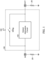
- FIG. 1 depicts a multi-level digital step attenuator (DSA) 100 in accordance with an exemplary embodiment of the disclosure.
- DSA digital step attenuator
- the multi-level DSA 100 has a hybrid attenuation circuit 102 and a bypass switch SWbp.
- the hybrid attenuation circuit 102 is coupled between an input node IN and an output node OUT of the multi-level DSA 100.
- the bypass switch SWbp is controlled to provide a bypass path between the input node IN and the output node OUT of the multi-level DSA 100 when the hybrid attenuation circuit 102 is in a disabled state.
- the hybrid attenuation circuit 102 provides multiple options for effective signal attenuation.
- the hybrid attenuation circuit 102 When being operated in a first active state, the hybrid attenuation circuit 102 is switched to form a T-type structure to provide a first amount of signal attenuation.
- the hybrid attenuation circuit 102 is switched to form a Pi-type structure to provide a second amount of signal attenuation.
- the multi-level DSA 100 is controlled by a 2-bit control signal 104 to switch the hybrid attenuation circuit 102 between the disabled state, the first active state, and the second active state.
- a 1.5-bit DSA is shown.
- the proposed multi-level DSA reduces the number of DSA stages. Fewer stages of DSAs are required for multi-level attenuation.
- the impedance Z0 presented at the input node IN is the impedance of the former stage.
- the impedance Z0 presented at the output node OUT is the impedance of the next stage.
- the impedance of each electronic component of the hybrid attenuation circuit 102 depends on the attenuation target and the impedance Z0 of the former/next stage.
- FIG. 2 depicts a multi-level DSA 200 in accordance with an exemplary embodiment of the disclosure.
- the hybrid attenuation circuit 202 has a first resistor R1 and a second resistor R2 coupled in series between the input node IN and the output node OUT of the multi-level DSA 200.
- the hybrid attenuation circuit 202 further has a third resistor R3.
- the third resistor R3 couples a connection node between the first resistor R1 and the second resistor R2 to a ground terminal.
- the first, second, and third resistors R1, R2, and R3 form a T-type structure that generates the first amount of signal attenuation.
- the hybrid attenuation circuit 202 further has a fourth resistor R4 and a fifth resistor R5.
- the fourth resistor R4 is coupled between the input node IN of the multi-level DSA 200 and the ground terminal
- the fifth electronic component R5 is coupled between the output node OUT of the multi-level DSA 200 and the ground terminal.
- the first, second, fourth and fifth resistors R1, R2, R4, and R5 form a Pi-type structure that generates the second amount of signal attenuation.
- the multi-level DSA 200 is controlled by a 2-bit control signal 204.
- the switches SW1, SW2, and SW3 can be turned off, and the bypass switch SWbp can be turned on to operate the hybrid attenuation circuit 202 in its disabled state.
- the hybrid attenuation circuit 202 operates in its first active state to form the T-type structure to provide the first amount of signal attenuation.
- the hybrid attenuation circuit 202 When the switches SW2 and SW3 are turned on, and the switch SW1 is turned off with the bypass switch SWbp by the 2-bit control signal 204, the hybrid attenuation circuit 202 operates in its second active state to form the Pi-type structure to provide the second amount of signal attenuation.
- the first amout of signal attenuation may be 2 ⁇ n dB, but not limited thereto. In the other exemplary embodiments, the first amout of signal attenuation may be any attenuation of non-radix-2.
- the T-type structure formed by the first, second, and third resistors R1, R2, and R3 provides signal attenuation of 2 ⁇ n dB.
- the impedance Z0 may be 50 ohm
- the first resistor R1 and the second resistor R2 each may have a resistance of 36 ohm
- the third R3 may have a resistance of 16 ohm.
- the fourth and the fifth resistors R4 and R5 each has a resistance of 96 ohm.
- the Pi-type structure formed by the first, second, fourth, and fifth resistors R1, R2, R4, and R5 provides signal attenuation of 10 dB (attenuation of non-radix-2).
- the detailed resistance values may be replaced by the other values, depending on the user's needs.
- FIG. 3 depicts a multi-level DSA 300 in accordance with another exemplary embodiment of the disclosure.
- the hybrid attenuation circuit 302 further includes a sixth resistor R6 in comparison with the hybrid attenuation circuit 202.
- the sixth resistor R6 is coupled between the input node IN and the output node OUT of the multi-level DSA 300, to being in parallel with the series of first and second resistors R1 and R2.
- the first, second, fourth, fifth, and sixth resistors R1, R2, R4, R5, and R6 also form a Pi-type structure that generates another amount of signal attenuation.
- the T-type structure (formed by the first, second, and third resistors R1, R2, and R3) provides signal attenuation of 2 ⁇ n dB
- the Pi-type structure (formed by first, second, fourth, fifth, and sixth resistors R1, R2, R4, R5, and R6) provides signal attenuation of 2 ⁇ (n-1) dB. It is convenient to digital design.
- the fourth and the fifth resistors R4 and R5 each has a resistance of 116 ohm.
- the T-type structure formed by the first, second, and third resistors R1, R2, and R3 provides 16dB signal attenuation that is in a power of 2
- the Pi-type structure formed by the first, second, fourth, fifth, and sixth resistors R1, R2, R4, R5, and R6 provides signal attenuation of 8 dB, which is also in a power of 2.
- the multi-level DSA 300 is controlled by a 2-bit control signal 304.
- the switches SW1, SW2, and SW3 are turned off, and the bypass switch SWbp is turned on by the 2-bit control signal 304.
- the switch SW1 is turned on, and the switches SW2, SW3 and SW4 are turned off with the bypass switch SWbp by the 2-bit control signal 304.
- the switches SW2, SW3 and SW4 are turned on, and the switch SW1 is turned off with the bypass switch SWbp by the 2-bit control signal 304.
- the resistors used in the hybrid attenuation circuit 202/302 may be replaced by other types of electronic components. Any attenuation circuit capable of being switched to form a T-type structure in a first active state and form a Pi-type structure in a second state should be considered within the scope of the disclosure.
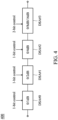
- FIG. 4 depicts a digital step attenuation device 400 in accordance with an exemplary embodiment of the disclosure, which includes 4 stages of digital step attenuation units DSA#0, DSA#1, DSA#2, and DSA#3.
- the digital step attenuation unit DSA#3 in the final stage is the proposed multi-level DSA 300, that is capable of providing signal attenuation of 8dB or 16dB.
- the first three digital step attenuation units DSA#0 to DSA#2 each is controlled by a 1-bit control signal.
- the final digital step attenuation unit DSA#3 is controlled by a 2-bit control signal.
- the digital step attenuation device 400 can generate 24-level signal attenuation from 0dB to 23dB according to a 5-bit control signal. It is more attenuation levels in comparison with a conventional 4-stage digital step attenuation device that only provides 16-level signal attenuation from 0dB to 15dB.
- signal attenuation of 20dB requires 5 stages of conventional digital step attenuation units.
- the 20dB attenuation can be successfully achieved by the 4-stage digital step attenuation device 400.
- the fewer LC matching networks for impedance matching are used in the fewer stage design, which results in the improved circuit area efficiency, and the reduced insertion loss.
- a digital step attenuation device includes m stages of digital step attenuation units, and the stages are numbered from 0 to (m-1), where m is any positive integer greater than 1. At least one digital step attenuation unit in the m stages is implemented by the multi-level DSA 100.
- the digital step attenuation unit implemented by the multi-level DSA 100 is in the number (m-1) stage (e.g., the final stage as FIG. 4 ).
- the multi-level DSA 100 in the number (m-1) stage is switched to its T-type structure, it provides signal attenuation of 2 ⁇ m dB.
- the multi-level DSA 100 in the number (m-1) stage is switched to its Pi-type structure, it provides signal attenuation of 2 ⁇ (m-1) dB.
- the digital step attenuation units in the number 0 to the number (m-2) stages are capable of providing signal attenuation of 2 ⁇ 0 dB to 2 ⁇ (m-2) dB, respectively.
- the m-stage digital step attenuation device is capable of providing more than 2 ⁇ m attenuation levels.
- the fewer LC matching networks are required in comparison with the conventional (m+1)-stage digital step attenuation device that is designed to provide more than 2 ⁇ m attenuation levels.
- Any digital step attenuation device using at least one of the proposed multi-level DSA 100 should be considered within the scope of the disclosure.
Landscapes
- Attenuators (AREA)
Abstract
A multi-level digital step attenuator (DSA) with a hybrid attenuation circuit is shown. The hybrid attenuation circuit is coupled between an input node and an output node of the multi-level DSA. The bypass switch of the multi-level DSA is controlled to provide a bypass path between the input node and the output node of the of the multi-level DSA when the hybrid attenuation circuit is in a disabled state. In the first active state, the hybrid attenuation circuit is switched to form a T-type structure to provide a first amount of signal attenuation. In the second active state, the hybrid attenuation circuit is switched to form a Pi-type structure to provide a second amount of signal attenuation.
Description
- The present invention relates to a digital step attenuation technology.
- In radio signal (RF) applications, a digital step attenuator (DSA) is a device that attenuates or reduces the amplitude of the RF signal that passes through it. The channel gain of the wireless receiver or transmitter (Rx/Tx), therefore, can be well controlled. The accuracy of the DSA will affect the reliability of the gain range of the channel, and therefore determine the usability of the Rx/Tx.
- Generally, the amount of attenuation is controlled digitally. A conventional DSA can be digitally switched between two modes. In an attenuation mode, the RF signal is attenuated by an attenuation circuit of the DSA. In a normal bypass mode, the RF signal is allowed to pass through by a bypass switch rather than by the attenuation circuit.
- Multiple DSAs may be coupled in series to provide more levels of signal attenuation. However, more stages may require more complex LC matching networks for wideband impedance matching.
- How to reduce the number of DSA stages is an important topic in this field of technology.
- A multi-level digital step attenuator (DSA) with a single bypass switch and a hybrid attenuation circuit is shown.
- A multi-level DSA in accordance with an exemplary embodiment of the disclosure has a hybrid attenuation circuit and a bypass switch. The hybrid attenuation circuit is coupled between an input node and an output node of the multi-level DSA. The bypass switch is controlled to provide a bypass path between the input node and the output node of the multi-level DSA when the hybrid attenuation circuit is in a disabled state. In a first active state, the hybrid attenuation circuit is switched to form a T-type structure to provide a first amount of signal attenuation. In a second active state, the hybrid attenuation circuit is switched to from a Pi-type structure to provide a second amount of signal attenuation.
- The proposed multi-level DSA is controlled by a 2-bit control signal to switch the hybrid attenuation circuit between the disabled state, the first active state and the second active state. A 2-bit control signals, 3 states, and single bypass switch 1.5-bit-DSA is shown. In comparison with the conventional DSA design, fewer stages of DSAs are required for wide-range and high resolution attenuation.
- In an exemplary embodiment, the hybrid attenuation circuit has a first electronic component and a second electronic component coupled in series between the input node and the output node of the multi-level DSA. The hybrid attenuation circuit further has a third electronic component that couples a connection node between the first electronic component and the second electronic component to a ground terminal when the hybrid attenuation circuit is in the first active state. A T-type structure is formed by the first, second and third electronic components.
- In an exemplary embodiment, the hybrid attenuation circuit further has a fourth electronic component and a fifth electronic component. The fourth electronic component is coupled between the input node of the multi-level DSA and the ground terminal when the hybrid attenuation circuit is in the second active state. The fifth electronic component is coupled between the output node of the multi-level DSA and the ground terminal when the hybrid attenuation circuit is in the second active state. A Pi-type structure is formed by the first, second, fourth and fifth electronic components.
- In another exemplary embodiment, the hybrid attenuation circuit further has a sixth electronic component coupled between the input node and the output node of the multi-level DSA when the hybrid attenuation circuit is in the second active state. The first, second, fourth, fifth, and sixth electronic components also form a Pi-type structure. In an exemplary embodiment, n is a positive integer. The T-type structure formed by the first, second, and third electronic components provides signal attenuation of 2^n dB, and the Pi-type structure formed by the first, second, fourth, fifth and sixth electronic components provides signal attenuation of 2^(n-1) dB. It is convenient for digital design.
- In an exemplary embodiment, a digital step attenuation device formed by multiple stages of digital step attenuation units is shown. At least one digital step attenuation unit in the multiple stages is implemented by the aforementioned multi-level DSA.
- A detailed description is given in the following embodiments with reference to the accompanying drawings.
- The present invention can be more fully understood by reading the subsequent detailed description and examples with references made to the accompanying drawings, wherein:
-
FIG. 1 depicts a multi-level digital step attenuator (DSA) 100 in accordance with an exemplary embodiment of the disclosure; -
FIG. 2 depicts a multi-level DSA 200 in accordance with an exemplary embodiment of the disclosure; -
FIG. 3 depicts a multi-level DSA 300 in accordance with another exemplary embodiment of the disclosure shows ; and -
FIG. 4 depicts a digitalstep attenuation device 400 in accordance with an exemplary embodiment of the disclosure. - The following description is made for the purpose of illustrating the general principles of the invention and should not be taken in a limiting sense. The scope of the invention is best determined by reference to the appended claims.
-
FIG. 1 depicts a multi-level digital step attenuator (DSA) 100 in accordance with an exemplary embodiment of the disclosure. - The multi-level DSA 100 has a
hybrid attenuation circuit 102 and a bypass switch SWbp. Thehybrid attenuation circuit 102 is coupled between an input node IN and an output node OUT of the multi-level DSA 100. The bypass switch SWbp is controlled to provide a bypass path between the input node IN and the output node OUT of themulti-level DSA 100 when thehybrid attenuation circuit 102 is in a disabled state. When the signal attenuation is enabled, thehybrid attenuation circuit 102 provides multiple options for effective signal attenuation. When being operated in a first active state, thehybrid attenuation circuit 102 is switched to form a T-type structure to provide a first amount of signal attenuation. When being operated in a second active state, thehybrid attenuation circuit 102 is switched to form a Pi-type structure to provide a second amount of signal attenuation. - In an exemplary embodiment, the multi-level DSA 100 is controlled by a 2-
bit control signal 104 to switch thehybrid attenuation circuit 102 between the disabled state, the first active state, and the second active state. A 1.5-bit DSA is shown. In comparison with the conventional DSA design which requires a long series of DSAs to provide the multiple options for effective signal attenuation, the proposed multi-level DSA reduces the number of DSA stages. Fewer stages of DSAs are required for multi-level attenuation. - The impedance Z0 presented at the input node IN is the impedance of the former stage. The impedance Z0 presented at the output node OUT is the impedance of the next stage. The impedance of each electronic component of the
hybrid attenuation circuit 102 depends on the attenuation target and the impedance Z0 of the former/next stage. -
FIG. 2 depicts a multi-level DSA 200 in accordance with an exemplary embodiment of the disclosure. - The
hybrid attenuation circuit 202 has a first resistor R1 and a second resistor R2 coupled in series between the input node IN and the output node OUT of the multi-level DSA 200. Thehybrid attenuation circuit 202 further has a third resistor R3. When the switch SW1 is turned on to operate thehybrid attenuation circuit 202 in the first active state, the third resistor R3 couples a connection node between the first resistor R1 and the second resistor R2 to a ground terminal. The first, second, and third resistors R1, R2, and R3 form a T-type structure that generates the first amount of signal attenuation. - The
hybrid attenuation circuit 202 further has a fourth resistor R4 and a fifth resistor R5. When the switches SW2 and SW3 are turned on to operate thehybrid attenuation circuit 202 in the second active state, the fourth resistor R4 is coupled between the input node IN of themulti-level DSA 200 and the ground terminal, and the fifth electronic component R5 is coupled between the output node OUT of themulti-level DSA 200 and the ground terminal. The first, second, fourth and fifth resistors R1, R2, R4, and R5 form a Pi-type structure that generates the second amount of signal attenuation. - In an exemplary embodiment, the
multi-level DSA 200 is controlled by a 2-bit control signal 204. By controlling the 2-bit control signal 204, the switches SW1, SW2, and SW3 can be turned off, and the bypass switch SWbp can be turned on to operate thehybrid attenuation circuit 202 in its disabled state. When the switch SW1 is turned on, and the switches SW2 and SW3 are turned off with the bypass switch SWbp by the 2-bit control signal 204, thehybrid attenuation circuit 202 operates in its first active state to form the T-type structure to provide the first amount of signal attenuation. When the switches SW2 and SW3 are turned on, and the switch SW1 is turned off with the bypass switch SWbp by the 2-bit control signal 204, thehybrid attenuation circuit 202 operates in its second active state to form the Pi-type structure to provide the second amount of signal attenuation. - The first amout of signal attenuation may be 2^n dB, but not limited thereto. In the other exemplary embodiments, the first amout of signal attenuation may be any attenuation of non-radix-2.
- In an exemplary embodiment, the T-type structure formed by the first, second, and third resistors R1, R2, and R3 provides signal attenuation of 2^n dB. For example, the impedance Z0 may be 50 ohm, the first resistor R1 and the second resistor R2 each may have a resistance of 36 ohm, and the third R3 may have a resistance of 16 ohm. The T-type structure formed by the first, second, and third resistors R1, R2, and R3 provides signal attenuation of 16 dB (=2^4 dB). In another exemplary embodiment, with the 36 ohm resistors R1 and R2 and the 50 ohm Z0, the fourth and the fifth resistors R4 and R5 each has a resistance of 96 ohm. The Pi-type structure formed by the first, second, fourth, and fifth resistors R1, R2, R4, and R5 provides signal attenuation of 10 dB (attenuation of non-radix-2). The detailed resistance values may be replaced by the other values, depending on the user's needs.
-
FIG. 3 depicts amulti-level DSA 300 in accordance with another exemplary embodiment of the disclosure. Thehybrid attenuation circuit 302 further includes a sixth resistor R6 in comparison with thehybrid attenuation circuit 202. When the switch SW4 is turned on with the switches SW2 and SW3 to operate thehybrid attenuation circuit 302 in its second active state, the sixth resistor R6 is coupled between the input node IN and the output node OUT of themulti-level DSA 300, to being in parallel with the series of first and second resistors R1 and R2. The first, second, fourth, fifth, and sixth resistors R1, R2, R4, R5, and R6 also form a Pi-type structure that generates another amount of signal attenuation. - In an exemplary embodiment wherein the T-type structure (formed by the first, second, and third resistors R1, R2, and R3) provides signal attenuation of 2^n dB, the Pi-type structure (formed by first, second, fourth, fifth, and sixth resistors R1, R2, R4, R5, and R6) provides signal attenuation of 2^(n-1) dB. It is convenient to digital design.
- In an exemplary embodiment, with the 36 ohm resistors R1 and R2, 16 ohm resistor R3, and the 50 ohm Z0, the fourth and the fifth resistors R4 and R5 each has a resistance of 116 ohm. Not only the T-type structure formed by the first, second, and third resistors R1, R2, and R3 provides 16dB signal attenuation that is in a power of 2, the Pi-type structure formed by the first, second, fourth, fifth, and sixth resistors R1, R2, R4, R5, and R6 provides signal attenuation of 8 dB, which is also in a power of 2.
- In an exemplary embodiment, the
multi-level DSA 300 is controlled by a 2-bit control signal 304. To switch thehybrid attenuation circuit 302 to its disabled state, the switches SW1, SW2, and SW3 are turned off, and the bypass switch SWbp is turned on by the 2-bit control signal 304. To switch thehybrid attenuation circuit 302 to its first active state to form the T-type structure to provide the first amount of signal attenuation, the switch SW1 is turned on, and the switches SW2, SW3 and SW4 are turned off with the bypass switch SWbp by the 2-bit control signal 304. To switch thehybrid attenuation circuit 302 to its second active state to form the Pi-type structure to provide the second amount of signal attenuation, the switches SW2, SW3 and SW4 are turned on, and the switch SW1 is turned off with the bypass switch SWbp by the 2-bit control signal 304. - In the other exemplary embodiments, the resistors used in the
hybrid attenuation circuit 202/302 may be replaced by other types of electronic components. Any attenuation circuit capable of being switched to form a T-type structure in a first active state and form a Pi-type structure in a second state should be considered within the scope of the disclosure. -
FIG. 4 depicts a digitalstep attenuation device 400 in accordance with an exemplary embodiment of the disclosure, which includes 4 stages of digital step attenuationunits DSA# 0,DSA# 1,DSA# 2, andDSA# 3. The digital step attenuationunit DSA# 3 in the final stage is the proposedmulti-level DSA 300, that is capable of providing signal attenuation of 8dB or 16dB. The digital step attenuationunit DSA# 0 in thenumber 0 stage is capable of providing signal attenuation of 1 dB (=2^0 dB). The digital step attenuationunit DSA# 1 in thenumber 1 stage is capable of providing signal attenuation of 2 dB (=2^1 dB). The digital step attenuationunit DSA# 2 in thenumber 2 stage is capable of providing signal attenuation of 4 dB (=2^2 dB). The first three digital step attenuationunits DSA# 0 toDSA# 2 each is controlled by a 1-bit control signal. The final digital step attenuationunit DSA# 3 is controlled by a 2-bit control signal. In such a design, the digitalstep attenuation device 400 can generate 24-level signal attenuation from 0dB to 23dB according to a 5-bit control signal. It is more attenuation levels in comparison with a conventional 4-stage digital step attenuation device that only provides 16-level signal attenuation from 0dB to 15dB. - In a conventional design, signal attenuation of 20dB requires 5 stages of conventional digital step attenuation units. However, the 20dB attenuation can be successfully achieved by the 4-stage digital
step attenuation device 400. The fewer LC matching networks for impedance matching are used in the fewer stage design, which results in the improved circuit area efficiency, and the reduced insertion loss. - In an exemplary embodiment, a digital step attenuation device includes m stages of digital step attenuation units, and the stages are numbered from 0 to (m-1), where m is any positive integer greater than 1. At least one digital step attenuation unit in the m stages is implemented by the
multi-level DSA 100. - In an exemplary embodiment, the digital step attenuation unit implemented by the
multi-level DSA 100 is in the number (m-1) stage (e.g., the final stage asFIG. 4 ). When themulti-level DSA 100 in the number (m-1) stage is switched to its T-type structure, it provides signal attenuation of 2^m dB. When themulti-level DSA 100 in the number (m-1) stage is switched to its Pi-type structure, it provides signal attenuation of 2^(m-1) dB. The digital step attenuation units in thenumber 0 to the number (m-2) stages are capable of providing signal attenuation of 2^0 dB to 2^(m-2) dB, respectively. In such a design, the m-stage digital step attenuation device is capable of providing more than 2^m attenuation levels. The fewer LC matching networks are required in comparison with the conventional (m+1)-stage digital step attenuation device that is designed to provide more than 2^m attenuation levels. - Any digital step attenuation device using at least one of the proposed
multi-level DSA 100 should be considered within the scope of the disclosure. - While the invention has been described by way of example and in terms of the preferred embodiments, it should be understood that the invention is not limited to the disclosed embodiments. On the contrary, it is intended to cover various modifications and similar arrangements (as would be apparent to those skilled in the art). Therefore, the scope of the appended claims should be accorded the broadest interpretation so as to encompass all such modifications and similar arrangements.
Claims (15)
- A multi-level digital step attenuator, comprising:a hybrid attenuation circuit, coupled between an input node and an output node of the multi-level digital step attenuator; anda bypass switch, controlled to provide a bypass path between the input node and the output node of the multi-level digital step attenuator when the hybrid attenuation circuit is in a disabled state;wherein:in a first active state, the hybrid attenuation circuit is switched to form a T-type structure to provide a first amount of signal attenuation; andin a second active state, the hybrid attenuation circuit is switched to form a Pi-type structure to provide a second amount of signal attenuation.
- The multi-level digital step attenuator as claimed in claim 1, wherein the hybrid attenuation circuit comprises:a first electronic component and a second electronic component, coupled in series between the input node and the output node of the multi-level digital step attenuator;a third electronic component, coupling a connection node between the first electronic component and the second electronic component to a ground terminal when the hybrid attenuation circuit is in the first active state.
- The multi-level digital step attenuator as claimed in claim 2, wherein the hybrid attenuation circuit further comprises:a fourth electronic component, coupled between the input node of the multi-level digital step attenuator and the ground terminal when the hybrid attenuation circuit is in the second active state; anda fifth electronic component, coupled between the output node of the multi-level digital step attenuator and the ground terminal when the hybrid attenuation circuit is in the second active state.
- The multi-level digital step attenuator as claimed in claim 3, wherein the hybrid attenuation circuit further comprises:
a sixth electronic component, coupled between the input node and the output node of the multi-level digital step attenuator when the hybrid attenuation circuit is in the second active state. - The multi-level digital step attenuator as claimed in claim 4, wherein:the T-type structure provides signal attenuation of 2^n dB or any attenuation of non-radix-2, and n is a positive integer; andthe Pi-type structure provides signal attenuation of 2^(n-1) dB or any attenuation of non-radix-2.
- The multi-level digital step attenuator as claimed in claim 4, wherein:the first electronic component and the second electronic component are resistors, each of which having a resistance of 36 ohm;the third electronic component is a resistor having a resistance of 16 ohm;the fourth electronic component and the fifth electronic component are resistors, each of which having a resistance of 116 ohm; andthe sixth electronic component is a resistor having a resistance of 195 ohm.
- The multi-level digital step attenuator as claimed in claim 3, wherein:
the T-type structure provides signal attenuation of 2^n dB or any attenuation of non-radix-2, and n is a positive integer. - The multi-level digital step attenuator as claimed in claim 3, wherein:the first electronic component and the second electronic component are resistors, each of which having a resistance of 36 ohm;the third electronic component is a resistor having a resistance of 16 ohm; andthe fourth electronic component and the fifth electronic component are resistors, each having a resistance of 96 ohm.
- The multi-level digital step attenuator as claimed in any one of the preceding claims, controlled by a 2-bit control signal to switch the hybrid attenuation circuit between the disabled state, the first active state and the second active state.
- A digital step attenuation device, comprising:multiple stages of digital step attenuation units,wherein at least one digital step attenuation unit in the multiple stages is implemented by the multi-level digital step attenuator as claimed in any one of the preceding claims.
- The digital step attenuation device as claimed in claim 10, wherein:the digital attenuation units form m stages numbered from 0 to (m-1), and m is a positive integer greater than 1; andthe digital step attenuation unit implemented by the multi-level digital step attenuator is in the number (m-1) stage.
- The digital step attenuation device as claimed in claim 11, wherein:the T-type structure of the multi-level digital step attenuator implementing the digital step attenuation unit in the number (m-1) stage provides signal attenuation of 2^m dB; andthe Pi-type structure of the multi-level digital step attenuator implementing the digital step attenuation unit in the number (m-1) stage provides signal attenuation of 2^(m-1) dB.
- The digital step attenuation device as claimed in claim 12, wherein:
when enabled, the digital step attenuation units in the number 0 to the number (m-2) stages provide signal attenuation of 2^0 dB to 2^(m-2) dB, respectively. - The digital step attenuation device as claimed in claim 13, providing more than 2^m attenuation levels.
- The digital step attenuation device as claimed in claim 10, wherein:the digital attenuation units form four stages numbered from 0 to 3;the digital step attenuation unit implemented by the multi-level digital step attenuator is in the number 3 stage;the T-type structure of the multi-level digital step attenuator implementing the digital step attenuation unit in the number 3 stage provides signal attenuation of 16 dB;the Pi-type structure of the multi-level digital step attenuator implementing the digital step attenuation unit in the number 3 stage provides signal attenuation of 8 dB;when enabled, the digital step attenuation units in the number 0 stage, the number 1 stage, and the number 2 stage provide signal attenuation of 1 dB, 2dB, and 4 dB, respectively; andthe digital step attenuation device provides more than 16 attenuation levels.
Applications Claiming Priority (2)
| Application Number | Priority Date | Filing Date | Title |
|---|---|---|---|
| US202363480314P | 2023-01-18 | 2023-01-18 | |
| US18/395,930 US12627281B2 (en) | 2023-01-18 | 2023-12-26 | Multi-level digital step attenuator and digital step attenuation device |
Publications (1)
| Publication Number | Publication Date |
|---|---|
| EP4407870A1 true EP4407870A1 (en) | 2024-07-31 |
Family
ID=89661180
Family Applications (1)
| Application Number | Title | Priority Date | Filing Date |
|---|---|---|---|
| EP24152638.3A Withdrawn EP4407870A1 (en) | 2023-01-18 | 2024-01-18 | A multi-level digital step attenuator and digital step attenuation device |
Country Status (2)
| Country | Link |
|---|---|
| US (1) | US12627281B2 (en) |
| EP (1) | EP4407870A1 (en) |
Citations (2)
| Publication number | Priority date | Publication date | Assignee | Title |
|---|---|---|---|---|
| US20180062622A1 (en) * | 2016-08-30 | 2018-03-01 | Skyworks Solutions, Inc. | Binary-weighted attenuator having compensation circuit |
| CN114244316A (en) * | 2021-12-08 | 2022-03-25 | 上海华虹宏力半导体制造有限公司 | Broadband switch control attenuation unit and broadband switch type attenuator |
-
2023
- 2023-12-26 US US18/395,930 patent/US12627281B2/en active Active
-
2024
- 2024-01-18 EP EP24152638.3A patent/EP4407870A1/en not_active Withdrawn
Patent Citations (2)
| Publication number | Priority date | Publication date | Assignee | Title |
|---|---|---|---|---|
| US20180062622A1 (en) * | 2016-08-30 | 2018-03-01 | Skyworks Solutions, Inc. | Binary-weighted attenuator having compensation circuit |
| CN114244316A (en) * | 2021-12-08 | 2022-03-25 | 上海华虹宏力半导体制造有限公司 | Broadband switch control attenuation unit and broadband switch type attenuator |
Also Published As
| Publication number | Publication date |
|---|---|
| US12627281B2 (en) | 2026-05-12 |
| US20240243732A1 (en) | 2024-07-18 |
Similar Documents
| Publication | Publication Date | Title |
|---|---|---|
| US7184731B2 (en) | Variable attenuator system and method | |
| US6737933B2 (en) | Circuit topology for attenuator and switch circuits | |
| EP0647024B1 (en) | Attenuator circuit apparatus | |
| US7221967B2 (en) | Enhanced gain selected cell phone booster system | |
| EP0741452B1 (en) | Attenuator unit, step attenuator, and electronic apparatus | |
| US4292596A (en) | Gain control circuit | |
| CN110535445B (en) | Variable gain low noise amplification apparatus with phase distortion compensation and amplification method | |
| EP1361666A1 (en) | Time division multiplexing connection transceiver and its receiving automatic gain control method | |
| CA2132356A1 (en) | Digital microwave multi-bit attenuator | |
| US12627281B2 (en) | Multi-level digital step attenuator and digital step attenuation device | |
| CN113671446B (en) | RF transceiver components and phased array radar | |
| US7436353B2 (en) | Transmitting-receiving module of radar system | |
| CN118661379A (en) | Current Mode RF Attenuator | |
| CN1666445B (en) | Optical Receiver Circuit | |
| US11121702B1 (en) | Digital step attenuator | |
| CN118367895A (en) | Multi-level digital step attenuator and digital step attenuation device | |
| US12424723B2 (en) | Circuit with first and second terminals coupled together via a branch-interconnection arrangement | |
| JP7148056B2 (en) | variable gain amplifier | |
| JP2008028908A (en) | Gain variable low-noise amplifier | |
| EP0482288B1 (en) | Electronic volume controller | |
| US8195116B2 (en) | Receiver circuitry with variable gain amplifier | |
| CN212324100U (en) | A power detection circuit and terminal equipment | |
| EP1739827B1 (en) | Radio frequency receiver including a limiter and related methods | |
| EP0969596A2 (en) | Variable attenuation circuit | |
| KR100703075B1 (en) | Signal attenuation circuit |
Legal Events
| Date | Code | Title | Description |
|---|---|---|---|
| PUAI | Public reference made under article 153(3) epc to a published international application that has entered the european phase |
Free format text: ORIGINAL CODE: 0009012 |
|
| STAA | Information on the status of an ep patent application or granted ep patent |
Free format text: STATUS: THE APPLICATION HAS BEEN PUBLISHED |
|
| AK | Designated contracting states |
Kind code of ref document: A1 Designated state(s): AL AT BE BG CH CY CZ DE DK EE ES FI FR GB GR HR HU IE IS IT LI LT LU LV MC ME MK MT NL NO PL PT RO RS SE SI SK SM TR |
|
| STAA | Information on the status of an ep patent application or granted ep patent |
Free format text: STATUS: THE APPLICATION IS DEEMED TO BE WITHDRAWN |
|
| 18D | Application deemed to be withdrawn |
Effective date: 20250201 |