EP4407801A1 - A dual band printed f-antenna using a trap with small band separation - Google Patents
A dual band printed f-antenna using a trap with small band separation Download PDFInfo
- Publication number
- EP4407801A1 EP4407801A1 EP24150166.7A EP24150166A EP4407801A1 EP 4407801 A1 EP4407801 A1 EP 4407801A1 EP 24150166 A EP24150166 A EP 24150166A EP 4407801 A1 EP4407801 A1 EP 4407801A1
- Authority
- EP
- European Patent Office
- Prior art keywords
- antenna
- leg
- antenna element
- frequency band
- inverted
- Prior art date
- Legal status (The legal status is an assumption and is not a legal conclusion. Google has not performed a legal analysis and makes no representation as to the accuracy of the status listed.)
- Pending
Links
- 230000009977 dual effect Effects 0.000 title claims abstract description 53
- 238000000926 separation method Methods 0.000 title description 3
- 239000003990 capacitor Substances 0.000 claims description 19
- 238000010586 diagram Methods 0.000 description 6
- 238000004519 manufacturing process Methods 0.000 description 5
- 230000000694 effects Effects 0.000 description 3
- 239000004593 Epoxy Substances 0.000 description 2
- 238000001914 filtration Methods 0.000 description 2
- 238000012986 modification Methods 0.000 description 2
- 230000004048 modification Effects 0.000 description 2
- 230000035945 sensitivity Effects 0.000 description 2
- RNFJDJUURJAICM-UHFFFAOYSA-N 2,2,4,4,6,6-hexaphenoxy-1,3,5-triaza-2$l^{5},4$l^{5},6$l^{5}-triphosphacyclohexa-1,3,5-triene Chemical compound N=1P(OC=2C=CC=CC=2)(OC=2C=CC=CC=2)=NP(OC=2C=CC=CC=2)(OC=2C=CC=CC=2)=NP=1(OC=1C=CC=CC=1)OC1=CC=CC=C1 RNFJDJUURJAICM-UHFFFAOYSA-N 0.000 description 1
- 230000000903 blocking effect Effects 0.000 description 1
- 230000005684 electric field Effects 0.000 description 1
- 230000005672 electromagnetic field Effects 0.000 description 1
- 239000003063 flame retardant Substances 0.000 description 1
- 239000011521 glass Substances 0.000 description 1
- 239000002648 laminated material Substances 0.000 description 1
Images


Classifications
-
- H—ELECTRICITY
- H01—ELECTRIC ELEMENTS
- H01Q—ANTENNAS, i.e. RADIO AERIALS
- H01Q1/00—Details of, or arrangements associated with, antennas
- H01Q1/36—Structural form of radiating elements, e.g. cone, spiral, umbrella; Particular materials used therewith
- H01Q1/38—Structural form of radiating elements, e.g. cone, spiral, umbrella; Particular materials used therewith formed by a conductive layer on an insulating support
-
- H—ELECTRICITY
- H01—ELECTRIC ELEMENTS
- H01Q—ANTENNAS, i.e. RADIO AERIALS
- H01Q5/00—Arrangements for simultaneous operation of antennas on two or more different wavebands, e.g. dual-band or multi-band arrangements
- H01Q5/30—Arrangements for providing operation on different wavebands
- H01Q5/307—Individual or coupled radiating elements, each element being fed in an unspecified way
- H01Q5/314—Individual or coupled radiating elements, each element being fed in an unspecified way using frequency dependent circuits or components, e.g. trap circuits or capacitors
- H01Q5/321—Individual or coupled radiating elements, each element being fed in an unspecified way using frequency dependent circuits or components, e.g. trap circuits or capacitors within a radiating element or between connected radiating elements
-
- H—ELECTRICITY
- H01—ELECTRIC ELEMENTS
- H01Q—ANTENNAS, i.e. RADIO AERIALS
- H01Q9/00—Electrically-short antennas having dimensions not more than twice the operating wavelength and consisting of conductive active radiating elements
- H01Q9/04—Resonant antennas
- H01Q9/0407—Substantially flat resonant element parallel to ground plane, e.g. patch antenna
- H01Q9/0421—Substantially flat resonant element parallel to ground plane, e.g. patch antenna with a shorting wall or a shorting pin at one end of the element
-
- H—ELECTRICITY
- H01—ELECTRIC ELEMENTS
- H01Q—ANTENNAS, i.e. RADIO AERIALS
- H01Q9/00—Electrically-short antennas having dimensions not more than twice the operating wavelength and consisting of conductive active radiating elements
- H01Q9/04—Resonant antennas
- H01Q9/30—Resonant antennas with feed to end of elongated active element, e.g. unipole
- H01Q9/42—Resonant antennas with feed to end of elongated active element, e.g. unipole with folded element, the folded parts being spaced apart a small fraction of the operating wavelength
Definitions
- the present disclosure pertains to antennas that may be used in a variety of wireless applications and more particularly pertains to dual band antennas having a small frequency band separation.
- a variety of electronic devices utilize antennas for wirelessly transmitting and/or receiving information.
- What would be desirable is a dual band antenna that can be easily and inexpensively incorporated into a variety of different electronic devices to support communication over each of two different frequency bands.
- the illustrative dual band inverted-F antenna includes a ground plane formed by a first conductive layer of a Printed Circuit Board (PCB).
- a first antenna element is formed by the first conductive layer, the first antenna element having a first leg and a second leg, wherein the first leg is connected to the ground plane, and the second leg extends along a length from the first leg to a distal end of the second leg parallel to the ground plane.
- a second antenna element is formed by the first conductive layer, the second antenna element connected to the second leg of the first antenna element at a first connection point along the length of the second leg that is proximal of the distal end of the second leg, the second antenna element electrically coupled to an antenna signal trace of the PCB.
- a third antenna element is formed by the first conductive layer, the third antenna element is spaced from the second leg of the first antenna element by a gap and positioned along the length of the second leg proximal of the distal end of the second leg but distal of the first connection point.
- a trap is operatively coupled across the gap between the second leg of the first antenna element and the third antenna element.
- a dual band inverted-F antenna that includes a planar inverted-F antenna with a trap, and is configured to have a first frequency band and a second frequency band.
- the first frequency band is separated from the second frequency band by less than 100 MHz.
- the dual band inverted-F antenna includes a planar inverted-F antenna with a trap, and is configured to have a first frequency band and a second frequency band.
- the first frequency band includes 865-870 MHz and the second frequency band includes 905-925 MHz.
- references in the specification to "an embodiment”, “some embodiments”, “other embodiments”, etc., indicate that the embodiment described may include a particular feature, structure, or characteristic, but every embodiment may not necessarily include the particular feature, structure, or characteristic. Moreover, such phrases are not necessarily referring to the same embodiment. Further, when a particular feature, structure, or characteristic is described in connection with an embodiment, it is contemplated that the feature, structure, or characteristic may be applied to other embodiments whether or not explicitly described unless clearly stated to the contrary.
- the dual band inverted-F antenna may be a printed antenna, sometimes printed on a Printed Circuit Board (PCB).
- the dual band inverted-F antenna may provide a first frequency band and a second frequency band, where the second frequency band is different from the first frequency band but is relatively close to the first frequency band (e.g. within 100 MHz).
- the dual band inverted-F antenna may include a trap to help create the first and second frequency bands.
- the trap may include one or more capacitors and one or more inductors connected in parallel, and may act as a band stop (e.g. notch) filter.
- a capacitor having a capacitance of 9.1 ⁇ 0.05 pF (pico farads) and one or more inductors with a total effective inductance of 3.4 nH (nano henry) with a tolerance of ⁇ 2 percent may be used.
- the dual band inverted-F antenna may be designed to utilize the first frequency band when used in electronic devices in parts of the world that utilize the first frequency band, and to utilize the second frequency band when used in electronic devices in parts of the world that utilize the second frequency band. It is contemplated that the dual band inverted-F antenna may be used in an electronic device that is configured to utilize both frequency bands.
- An example of a dual band inverted-F antenna includes a ground plane formed by one or more conductive layers of a Printed Circuit Board (PCB).
- PCB Printed Circuit Board
- conductive layer(s) and insulative layer(s) of the PCB may have a total thickness of 1.6 millimeters.
- the PCB insulative layer(s) may be formed of, or otherwise include, FR4.
- FR4 is a fiberglass-reinforced epoxy laminate material, and is considered to be flame-retardant.
- FR-4 glass epoxy has a good strength to weight ratio.
- a first antenna element is formed by a first conductive layer.
- the first antenna element has a first leg and a second leg, where the first leg is connected to the ground plane, and the second leg extends parallel to the ground plane along a length from the first leg to a distal end of the second leg.
- a second antenna element is formed by the first conductive layer and is connected to the second leg of the first antenna element at a first connection point along the length of the second leg. The first connection point is proximal of the distal end of the second leg.
- the second antenna element is electrically coupled to an antenna signal trace of the PCB.
- the first antenna element and the second antenna element collectively form an antenna that is configured to operate in the first frequency band (e.g. 902-928 MHz).
- a third antenna element is formed by the first conductive layer and is spaced from the second leg of the first antenna element by a gap.
- the third antenna element is positioned along the length of the second leg of the first antenna element proximal of the distal end of the second leg but distal of the first connection point.
- the third antenna element is configured (sized and shaped) to operate in a second frequency band (e.g. 865-870 MHz).
- the third antenna element is electrically connected to the second leg of the first antenna element through a trap, and thus electrically connected to the second antenna element and the antenna signal trace.
- the trap is operatively coupled across the gap between the second leg of the first antenna element and the third antenna element.
- the trap may be coupled to the second leg at a second connection point along the length of the second leg.
- the second connection point is proximal of the distal end of the second leg but distal of the first connection point.
- the trap may include an inductor that is coupled between the second leg of the first antenna element and the third antenna element, and a capacitor that is coupled between the second leg of the first antenna element and the third antenna element in parallel with the inductor.
- the second connection point is located proximal of the distal end of the second leg by a distance of at least 10 percent of the total length of the second leg.
- the first connection point is located proximal of the distal end of the second leg by a distance of at least 50 percent of the total length of the second leg.
- the inductor and the capacitor may be surface mount components that are positioned across the gap and soldered direct to the first antenna element and the third antenna element.
- the antenna signal trace may be operatively coupled to a dual band radio circuitry that is mounted to the PCB. In some instances, the antenna signal trace of the PCB may be operatively coupled to filter circuitry mounted to the PCB. In some instances, the antenna signal trace of the PCB may be operatively coupled to amplifier circuitry mounted to the PCB.
- the dual band inverted-F antenna may be sensitive in a first frequency band and a second frequency band, wherein the first frequency band is non-overlapping with the second frequency band.
- the first frequency band may include 865-870 MHz and the second frequency band may include 902-928 MHz.
- the first frequency band may have a bandwidth of at least 5 MHz with a -10 dB return loss or less within the band
- the second frequency band may have a bandwidth of at least 20 MHz with a -10 dB return loss or less within the band.
- the first frequency band may be separated from the second frequency band by less than 100 MHz.
- FIG. 1 is a schematic diagram showing an illustrative dual band inverted-F antenna 10.
- the illustrative dual band inverted-F antenna 10 includes a first antenna element 12, a second antenna element 14 and a third antenna element 24.
- the first antenna element 12 includes a first leg 12a and a second leg 12b.
- the first leg 12a is connected to a ground plane 16 that, as seen, may be considered as being divided into a first ground plane section 16a and a second ground plane section 16b.
- the second leg 12b extends along a length from the first leg 12a to a distal end 18 of the second leg 12b. In this example, the second leg 12b extends parallel to the ground plane 16.
- the second antenna element 14 is connected to the second leg 12b at a first connection point 20 along the length of the second leg 12b that is proximal (e.g. to the left of in Figure 1 ) of the distal end 18 of the second leg 12b.
- the ground plane 16, the first antenna element 12 and the second antenna element 14 are each formed by a first conductive layer of a Printed Circuit Board (PCB), although this is not required.
- the second antenna element 14 is electrically coupled to an antenna trace signal 22 of the PCB.
- the antenna trace signal 22 may be considered as having an impedance that matches that of the dual band inverted-F antenna 10. This may help prevent signal reflections at the interface between the antenna trace signal 22 and the dual band inverted-F antenna 10, thereby improving the effective antenna efficiency.
- the third antenna element 24 is spaced from the second leg 12b of the first antenna element 12 by a gap.
- the third antenna element 24 is positioned along the length of the second leg 12b of the first antenna element 12 proximal of the distal end 18 of the second leg 12b but distal of the first connection point 20.
- the third antenna element 24 is configured (sized and shaped) to operate in the second frequency band.
- the third antenna element is electrically connected to the second leg 12b of the first antenna element 12 via the trap, and thus to the second antenna element 14 and the antenna trace signal 22.
- the trap 28 (e.g. trap shown in Figure 2 ) is operatively coupled across the gap between the second leg 12b of the first antenna element 12 at the third antenna element 24.
- the trap 28 may be coupled to the second leg 12b at a second connection point along the length of the second leg 12b.
- the second connection point is proximal of the distal end 18 of the second leg 12b but distal of the first connection point 20.
- the trap 28 may include an inductor 32a that is coupled between the second leg 12b of the first antenna element 12 and the third antenna element 24, and a capacitor 30 that is coupled between the second leg 12b of the first antenna element 12 and the third antenna element 24 in parallel with the inductor 32a.
- a capacitor opposes a change in voltage and stores energy in the form of an electric field.
- an inductor opposes a change in current and stores energy in the form of a magnetic field.
- the second connection point is located proximal of the distal end 18 of the second leg 12b by a distance of at least 10 percent of the total length of the second leg 12b.
- the first connection point 20 is located proximal of the distal end 18 of the second leg 12b by a distance of at least 50 percent of the total length of the second leg 12b.
- the inductor 32a and the capacitor 30 may be surface mount components that are positioned across the gap and soldered direct to the second leg 12b of the first antenna element 12 and the third antenna element 24.
- the illustrative dual band inverted-F antenna 10 mayh be operatively coupled to an electrical component 26.
- the electrical component 26 may be mounted onto the same PCB that the rest of the dual band inverted-F antenna 10 is formed from.
- the electrical component 26 may be a radio.
- the electrical component 26 may be a dual band radio.
- the electrical component 26 may include filtering circuitry (e.g. bandpass filtering).
- the electrical component 26 may include amplifier circuitry.
- the electrical component 26 may include impedance-matching circuitry. These are just examples.
- the dual band inverted-F antenna 10 may be sensitive in a first frequency band and a second frequency band, wherein the first frequency band is non-overlapping with the second frequency band.
- the first frequency band may include 865-870 MHz and the second frequency band may include 902-928 MHz.
- the first frequency band may have a bandwidth of at least 5 MHz with a -10 dB return loss or less within the band
- the second frequency band may have a bandwidth of at least 20 MHz with a -10 dB return loss or less within the band.
- the first frequency band may be separated from the second frequency band by less than 100 MHz.
- FIG 2 is a schematic diagram showing an illustrative trap 28.
- the trap 28 may act as a band stop (e.g. notch) filter that has the effect of blocking first frequency electrical current in the second leg 12b of the first antenna element 12 from flowing to the third antenna element 24.
- the trap is operatively coupled across the gap between the second leg 12b of the first antenna element 12 at the third antenna element 24 (see Figure 1 ).
- the trap 28 includes a capacitor 30 that is connected in parallel with an inductor 32.
- a single inductor 32a may be used.
- a second inductor 32b may also be used in combination with the inductor 32a.
- the capacitor 30 may have a capacitance of 9.1 ⁇ 0.05 pF
- the inductor 32a and the inductor 32b may each have an inductance of 6.8 nH ⁇ 2 percent (for a total of 3.4 nH when connected in parallel as shown).
- the inductor 32 and the capacitor 30 may be surface mount components that are positioned across the gap and soldered direct to the second leg 12b of the first antenna element 12 and the third antenna element 24.
- the overall sensitivity to the trap 28 is reduced.
- the manufacturing tolerances for the capacitor and inductor component 30,32 do not necessarily scale with the magnitude of the capacitance and/or inductance values, it can be desirable to use a capacitor component 30 in the trap 28 that has a larger capacitance value so that the ⁇ manufacturing tolerances of the capacitor component 30 have an overall smaller effect on the filter characteristics of the trap 28.
- multiple larger inductor components 32a and 32b may be provided in a parallel configuration (as shown in Figure 2 ) to achieve a desired inductance value so that the ⁇ manufacturing tolerances of the inductor components 32a 32b have an overall smaller effect on the filter characteristics of the trap 28. This may help reduce changes in the first and second frequency bands due to manufacturing tolerances of the trap components, which can be important particular where the frequency bands are relatively close to each other, such as within less than 100 MHz of each other.
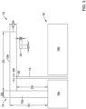
- Figure 3 is a schematic diagram of the dual band inverted-F antenna 10, showing various dimensions of the dual band inverted-F antenna 10.
- the first leg 12a may have a length D1 in a range of about 10 to 15 millimeters and a width D2 that is in a range of about 2 to 3 millimeters.
- the second leg 12b has a length D3 in a range of about 50 to 60 millimeters and a width D4 that is in a range of about 2 to 3 millimeters.
- the second antenna element 14 has a length D5 (between the second leg 12b and the ground plane 16) that is in a range of about 8 to 12 millimeters and a width D6 that is in a range of about 0.5 to 1 millimeter.
- the conductive pad of the third antenna element 24 has a length D7 that is in a range of about 3 to 4 millimeters and a width D8 that is in a range of about 1 to 2 millimeters.
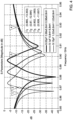
- Figure 4 is a graphical representation of a simulated frequency response for the inverted-F antenna of Figures 1-3 . More particularly, Figure 4 shows a plot of magnitude in decibels (dB) versus frequency in gigaherz (GHz) for a dual band inverted-F antenna such as the dual band inverted-F antenna 10.
- the simulated antenna had a ground plane that was 100 millimeters by 100 millimeters PEC, with a thickness of 1.6 millimeters.
- the antenna area was 13.5 millimeters wide.
- Antenna dimensions were 59.4 millimeters by 11 millimeters, antenna trace (D2 and D4) was 2.6 millimeters wide and the feed width (D6) was 0.65 millimeters.
- FIG. 4 shows antenna return loss with the trap 28 including a 9.1 pF capacitor (nominal) and a pair of inductors each having an inductance of 6.8 nH (nominal).
- Figure 4 also shows return loss versus frequency for the two ends of tolerance, including a 9.05 pF capacitor and a pair of 6.664 nH inductors (98% of 6.8 nH), and a 9.15 pF capacitor and a pair of 6.936 nH inductors.
Landscapes
- Support Of Aerials (AREA)
Abstract
A dual band inverted-F antenna includes a first antenna element having a first leg connected to a ground plane and a second leg extending along a length from the first leg to a distal end of the second leg. A second antenna element connects to the second leg at a first connection point that is proximal of the distal end of the second leg, the second antenna element electrically coupled to an antenna signal trace of a PCB. A third antenna element is spaced from the second leg of the first antenna element by a gap and positioned along the length of the second leg proximal of the distal end of the second leg but distal of the first connection point. A trap is operatively coupled across the gap between the second leg of the first antenna element and the third antenna element.
Description
- This application claims the benefit of
U.S. Provisional Patent Application Serial No. 63/481,724, filed January 26, 2023 - The present disclosure pertains to antennas that may be used in a variety of wireless applications and more particularly pertains to dual band antennas having a small frequency band separation.
- A variety of electronic devices utilize antennas for wirelessly transmitting and/or receiving information. In some cases, it may be desirable for an electronic device to have the capability of communicating over two or more different frequency bands. What would be desirable is a dual band antenna that can be easily and inexpensively incorporated into a variety of different electronic devices to support communication over each of two different frequency bands.
- This disclosure pertains to generally antennas that may be used in a variety of wireless applications and more particularly pertains to dual band antennas having a small frequency band separation. An example may be found in a dual band inverted-F antenna. The illustrative dual band inverted-F antenna includes a ground plane formed by a first conductive layer of a Printed Circuit Board (PCB). A first antenna element is formed by the first conductive layer, the first antenna element having a first leg and a second leg, wherein the first leg is connected to the ground plane, and the second leg extends along a length from the first leg to a distal end of the second leg parallel to the ground plane. A second antenna element is formed by the first conductive layer, the second antenna element connected to the second leg of the first antenna element at a first connection point along the length of the second leg that is proximal of the distal end of the second leg, the second antenna element electrically coupled to an antenna signal trace of the PCB. A third antenna element is formed by the first conductive layer, the third antenna element is spaced from the second leg of the first antenna element by a gap and positioned along the length of the second leg proximal of the distal end of the second leg but distal of the first connection point. A trap is operatively coupled across the gap between the second leg of the first antenna element and the third antenna element.
- Another example may be found in a dual band inverted-F antenna that includes a planar inverted-F antenna with a trap, and is configured to have a first frequency band and a second frequency band. The first frequency band is separated from the second frequency band by less than 100 MHz.
- Another example may be found in a dual band inverted-F antenna. The dual band inverted-F antenna includes a planar inverted-F antenna with a trap, and is configured to have a first frequency band and a second frequency band. The first frequency band includes 865-870 MHz and the second frequency band includes 905-925 MHz.
- The preceding summary is provided to facilitate an understanding of some of the features of the present disclosure and is not intended to be a full description. A full appreciation of the disclosure can be gained by taking the entire specification, claims, drawings, and abstract as a whole.
- The disclosure may be more completely understood in consideration of the following description of various illustrative embodiments of the disclosure in connection with the accompanying drawings, in which:
-
Figure 1 is a schematic diagram showing an illustrative dual band inverted-F antenna; -
Figure 2 is a schematic diagram showing an illustrative trap used as part of the illustrative dual band inverted-F antenna ofFigure 1 ; -
Figure 3 is a schematic diagram showing the illustrative dual band inverted-F antenna ofFigure 1 , with various dimensions annotated; and -
Figure 4 is a graphical representation of a simulated frequency response for the inverted-F antenna ofFigures 1-3 . - While the disclosure is amenable to various modifications and alternative forms, specifics thereof have been shown by way of example in the drawings and will be described in detail. It should be understood, however, that the intention is not to limit aspects of the disclosure to the particular illustrative embodiments described. On the contrary, the intention is to cover all modifications, equivalents, and alternatives falling within the spirit and scope of the disclosure.
- The following description should be read with reference to the drawings wherein like reference numerals indicate like elements. The drawings, which are not necessarily to scale, are not intended to limit the scope of the disclosure. In some of the figures, elements not believed necessary to an understanding of relationships among illustrated components may have been omitted for clarity.
- All numbers are herein assumed to be modified by the term "about", unless the content clearly dictates otherwise. The term "about" means within a range of plus or minus 10 percent of the expressed number. The recitation of numerical ranges by endpoints includes all numbers subsumed within that range (e.g., 1 to 5 includes 1, 1.5, 2, 2.75, 3, 3.80, 4, and 5).
- As used in this specification and the appended claims, the singular forms "a", "an", and "the" include the plural referents unless the content clearly dictates otherwise. As used in this specification and the appended claims, the term "or" is generally employed in its sense including "and/or" unless the content clearly dictates otherwise.
- It is noted that references in the specification to "an embodiment", "some embodiments", "other embodiments", etc., indicate that the embodiment described may include a particular feature, structure, or characteristic, but every embodiment may not necessarily include the particular feature, structure, or characteristic. Moreover, such phrases are not necessarily referring to the same embodiment. Further, when a particular feature, structure, or characteristic is described in connection with an embodiment, it is contemplated that the feature, structure, or characteristic may be applied to other embodiments whether or not explicitly described unless clearly stated to the contrary.
- A dual band inverted-F antenna is described herein. The dual band inverted-F antenna may be a printed antenna, sometimes printed on a Printed Circuit Board (PCB). In some cases, the dual band inverted-F antenna may provide a first frequency band and a second frequency band, where the second frequency band is different from the first frequency band but is relatively close to the first frequency band (e.g. within 100 MHz). In some instances, the dual band inverted-F antenna may include a trap to help create the first and second frequency bands. As an example, the trap may include one or more capacitors and one or more inductors connected in parallel, and may act as a band stop (e.g. notch) filter. In one example, for a dual band inverted-F antenna having a first frequency band between 865 MHz and 870 MHz and a second frequency band between 902 MHz and 928 MHz, a capacitor having a capacitance of 9.1 ± 0.05 pF (pico farads) and one or more inductors with a total effective inductance of 3.4 nH (nano henry) with a tolerance of ± 2 percent may be used.
- In some instances, the dual band inverted-F antenna may be designed to utilize the first frequency band when used in electronic devices in parts of the world that utilize the first frequency band, and to utilize the second frequency band when used in electronic devices in parts of the world that utilize the second frequency band. It is contemplated that the dual band inverted-F antenna may be used in an electronic device that is configured to utilize both frequency bands.
- An example of a dual band inverted-F antenna includes a ground plane formed by one or more conductive layers of a Printed Circuit Board (PCB). In some cases, conductive layer(s) and insulative layer(s) of the PCB may have a total thickness of 1.6 millimeters. The PCB insulative layer(s) may be formed of, or otherwise include, FR4. FR4 is a fiberglass-reinforced epoxy laminate material, and is considered to be flame-retardant. FR-4 glass epoxy has a good strength to weight ratio.
- In one example, a first antenna element is formed by a first conductive layer. The first antenna element has a first leg and a second leg, where the first leg is connected to the ground plane, and the second leg extends parallel to the ground plane along a length from the first leg to a distal end of the second leg. A second antenna element is formed by the first conductive layer and is connected to the second leg of the first antenna element at a first connection point along the length of the second leg. The first connection point is proximal of the distal end of the second leg. The second antenna element is electrically coupled to an antenna signal trace of the PCB. The first antenna element and the second antenna element collectively form an antenna that is configured to operate in the first frequency band (e.g. 902-928 MHz). A third antenna element is formed by the first conductive layer and is spaced from the second leg of the first antenna element by a gap. The third antenna element is positioned along the length of the second leg of the first antenna element proximal of the distal end of the second leg but distal of the first connection point. The third antenna element is configured (sized and shaped) to operate in a second frequency band (e.g. 865-870 MHz). The third antenna element is electrically connected to the second leg of the first antenna element through a trap, and thus electrically connected to the second antenna element and the antenna signal trace.
- To help block electrical current of the first frequency in the second leg of the first antenna element from flowing across the gap to the third antenna element, the trap is operatively coupled across the gap between the second leg of the first antenna element and the third antenna element. The trap may be coupled to the second leg at a second connection point along the length of the second leg. The second connection point is proximal of the distal end of the second leg but distal of the first connection point.
- In one example, the trap may include an inductor that is coupled between the second leg of the first antenna element and the third antenna element, and a capacitor that is coupled between the second leg of the first antenna element and the third antenna element in parallel with the inductor. In some instances, the second connection point is located proximal of the distal end of the second leg by a distance of at least 10 percent of the total length of the second leg. In some instances, the first connection point is located proximal of the distal end of the second leg by a distance of at least 50 percent of the total length of the second leg. In some cases, the inductor and the capacitor may be surface mount components that are positioned across the gap and soldered direct to the first antenna element and the third antenna element.
- In some instances, the antenna signal trace may be operatively coupled to a dual band radio circuitry that is mounted to the PCB. In some instances, the antenna signal trace of the PCB may be operatively coupled to filter circuitry mounted to the PCB. In some instances, the antenna signal trace of the PCB may be operatively coupled to amplifier circuitry mounted to the PCB.
- In some instances, the dual band inverted-F antenna may be sensitive in a first frequency band and a second frequency band, wherein the first frequency band is non-overlapping with the second frequency band. As an example, the first frequency band may include 865-870 MHz and the second frequency band may include 902-928 MHz. In some instances, the first frequency band may have a bandwidth of at least 5 MHz with a -10 dB return loss or less within the band, and the second frequency band may have a bandwidth of at least 20 MHz with a -10 dB return loss or less within the band. In some cases, the first frequency band may be separated from the second frequency band by less than 100 MHz.
-
Figure 1 is a schematic diagram showing an illustrative dual band inverted-F antenna 10. The illustrative dual band inverted-F antenna 10 includes afirst antenna element 12, asecond antenna element 14 and athird antenna element 24. Thefirst antenna element 12 includes afirst leg 12a and asecond leg 12b. Thefirst leg 12a is connected to aground plane 16 that, as seen, may be considered as being divided into a firstground plane section 16a and a secondground plane section 16b. Thesecond leg 12b extends along a length from thefirst leg 12a to adistal end 18 of thesecond leg 12b. In this example, thesecond leg 12b extends parallel to theground plane 16. Thesecond antenna element 14 is connected to thesecond leg 12b at afirst connection point 20 along the length of thesecond leg 12b that is proximal (e.g. to the left of inFigure 1 ) of thedistal end 18 of thesecond leg 12b. In this example, theground plane 16, thefirst antenna element 12 and thesecond antenna element 14 are each formed by a first conductive layer of a Printed Circuit Board (PCB), although this is not required. Thesecond antenna element 14 is electrically coupled to anantenna trace signal 22 of the PCB. In some instances, theantenna trace signal 22 may be considered as having an impedance that matches that of the dual band inverted-F antenna 10. This may help prevent signal reflections at the interface between theantenna trace signal 22 and the dual band inverted-F antenna 10, thereby improving the effective antenna efficiency. - The
third antenna element 24 is spaced from thesecond leg 12b of thefirst antenna element 12 by a gap. Thethird antenna element 24 is positioned along the length of thesecond leg 12b of thefirst antenna element 12 proximal of thedistal end 18 of thesecond leg 12b but distal of thefirst connection point 20. Thethird antenna element 24 is configured (sized and shaped) to operate in the second frequency band. The third antenna element is electrically connected to thesecond leg 12b of thefirst antenna element 12 via the trap, and thus to thesecond antenna element 14 and theantenna trace signal 22. - To help block electrical current of the first frequency in the
second leg 12b of thefirst antenna element 12 from flowing to thethird antenna element 24, the trap 28 (e.g. trap shown inFigure 2 ) is operatively coupled across the gap between thesecond leg 12b of thefirst antenna element 12 at thethird antenna element 24. Thetrap 28 may be coupled to thesecond leg 12b at a second connection point along the length of thesecond leg 12b. The second connection point is proximal of thedistal end 18 of thesecond leg 12b but distal of thefirst connection point 20. - In one example, and as shown in
Figure 2 , thetrap 28 may include aninductor 32a that is coupled between thesecond leg 12b of thefirst antenna element 12 and thethird antenna element 24, and acapacitor 30 that is coupled between thesecond leg 12b of thefirst antenna element 12 and thethird antenna element 24 in parallel with theinductor 32a. In some instances, a capacitor opposes a change in voltage and stores energy in the form of an electric field. In some instances, an inductor opposes a change in current and stores energy in the form of a magnetic field. In some instances, the second connection point is located proximal of thedistal end 18 of thesecond leg 12b by a distance of at least 10 percent of the total length of thesecond leg 12b. In some instances, thefirst connection point 20 is located proximal of thedistal end 18 of thesecond leg 12b by a distance of at least 50 percent of the total length of thesecond leg 12b. In some cases, theinductor 32a and thecapacitor 30 may be surface mount components that are positioned across the gap and soldered direct to thesecond leg 12b of thefirst antenna element 12 and thethird antenna element 24. - The illustrative dual band inverted-
F antenna 10 mayh be operatively coupled to anelectrical component 26. In some cases, theelectrical component 26 may be mounted onto the same PCB that the rest of the dual band inverted-F antenna 10 is formed from. In some instances, theelectrical component 26 may be a radio. In some instances, theelectrical component 26 may be a dual band radio. In some instances, theelectrical component 26 may include filtering circuitry (e.g. bandpass filtering). In some instances, theelectrical component 26 may include amplifier circuitry. In some instances, theelectrical component 26 may include impedance-matching circuitry. These are just examples. - In some instances, the dual band inverted-
F antenna 10 may be sensitive in a first frequency band and a second frequency band, wherein the first frequency band is non-overlapping with the second frequency band. As an example, the first frequency band may include 865-870 MHz and the second frequency band may include 902-928 MHz. In some cases, the first frequency band may have a bandwidth of at least 5 MHz with a -10 dB return loss or less within the band, and the second frequency band may have a bandwidth of at least 20 MHz with a -10 dB return loss or less within the band. In some cases, the first frequency band may be separated from the second frequency band by less than 100 MHz. -
Figure 2 is a schematic diagram showing anillustrative trap 28. Thetrap 28 may act as a band stop (e.g. notch) filter that has the effect of blocking first frequency electrical current in thesecond leg 12b of thefirst antenna element 12 from flowing to thethird antenna element 24. The trap is operatively coupled across the gap between thesecond leg 12b of thefirst antenna element 12 at the third antenna element 24 (seeFigure 1 ). In the example shown, thetrap 28 includes acapacitor 30 that is connected in parallel with aninductor 32. In some cases, asingle inductor 32a may be used. In some cases, depending on the desired total inductance, asecond inductor 32b may also be used in combination with theinductor 32a. In an example, thecapacitor 30 may have a capacitance of 9.1 ± 0.05 pF, theinductor 32a and theinductor 32b may each have an inductance of 6.8 nH ± 2 percent (for a total of 3.4 nH when connected in parallel as shown). This is just an example. In some cases, theinductor 32 and thecapacitor 30 may be surface mount components that are positioned across the gap and soldered direct to thesecond leg 12b of thefirst antenna element 12 and thethird antenna element 24. - By moving the
third antenna element 24 and thetrap 28 away from thedistal end 18 of thesecond leg 12b, where the electromagnetic field of the antenna is largest, the overall sensitivity to thetrap 28 is reduced. This allows the manufacturing tolerances of the capacitor and inductor values of thecomponents trap 28 to have a smaller influence, while still achieving the desired frequency response for the dual band inverted-F antenna 10. For example, since the manufacturing tolerances for the capacitor andinductor component capacitor component 30 in thetrap 28 that has a larger capacitance value so that the ± manufacturing tolerances of thecapacitor component 30 have an overall smaller effect on the filter characteristics of thetrap 28. Use of a larger capacitance value is possible because the overall sensitivity of thetrap 28 is reduced when moving thethird antenna element 24 and thetrap 28 away from thedistal end 18 of thesecond leg 12b. Likewise, in some cases, multiplelarger inductor components Figure 2 ) to achieve a desired inductance value so that the ± manufacturing tolerances of theinductor components 32atrap 28. This may help reduce changes in the first and second frequency bands due to manufacturing tolerances of the trap components, which can be important particular where the frequency bands are relatively close to each other, such as within less than 100 MHz of each other. -
Figure 3 is a schematic diagram of the dual band inverted-F antenna 10, showing various dimensions of the dual band inverted-F antenna 10. Thefirst leg 12a may have a length D1 in a range of about 10 to 15 millimeters and a width D2 that is in a range of about 2 to 3 millimeters. Thesecond leg 12b has a length D3 in a range of about 50 to 60 millimeters and a width D4 that is in a range of about 2 to 3 millimeters. Thesecond antenna element 14 has a length D5 (between thesecond leg 12b and the ground plane 16) that is in a range of about 8 to 12 millimeters and a width D6 that is in a range of about 0.5 to 1 millimeter. The conductive pad of thethird antenna element 24 has a length D7 that is in a range of about 3 to 4 millimeters and a width D8 that is in a range of about 1 to 2 millimeters. -
Figure 4 is a graphical representation of a simulated frequency response for the inverted-F antenna ofFigures 1-3 . More particularly,Figure 4 shows a plot of magnitude in decibels (dB) versus frequency in gigaherz (GHz) for a dual band inverted-F antenna such as the dual band inverted-F antenna 10. The simulated antenna had a ground plane that was 100 millimeters by 100 millimeters PEC, with a thickness of 1.6 millimeters. The antenna area was 13.5 millimeters wide. Antenna dimensions were 59.4 millimeters by 11 millimeters, antenna trace (D2 and D4) was 2.6 millimeters wide and the feed width (D6) was 0.65 millimeters. Antenna PEC thickness was 0.035 millimeters.Figure 4 shows antenna return loss with thetrap 28 including a 9.1 pF capacitor (nominal) and a pair of inductors each having an inductance of 6.8 nH (nominal).Figure 4 also shows return loss versus frequency for the two ends of tolerance, including a 9.05 pF capacitor and a pair of 6.664 nH inductors (98% of 6.8 nH), and a 9.15 pF capacitor and a pair of 6.936 nH inductors. As can be seen, across all tolerances of the capacitor and the inductors of thetrap 28, a design goal of having a return less of less than -10 dB in both the first frequency band of 865-870 MHz (noted between arrows "1" and "2" inFigure 4 ) and the second frequency band of 902-928 MHz (noted between arrows "3" and "4" inFigure 4 ). - It should be understood that this disclosure is, in many respects, only illustrative. Changes may be made in details, particularly in matters of shape, size, and arrangement of steps without exceeding the scope of the disclosure. This may include, to the extent that it is appropriate, the use of any of the features of one example embodiment being used in other embodiments.
Claims (15)
- A dual band inverted-F antenna, comprising:a ground p1lane formed by a first conductive layer of a Printed Circuit Board (PCB);a first antenna element formed by the first conductive layer, the first antenna element having a first leg and a second leg, wherein the first leg is connected to the ground plane, and the second leg extends along a length from the first leg to a distal end of the second leg parallel to the ground plane;a second antenna element formed by the first conductive layer, the second antenna element connected to the second leg of the first antenna element at a first connection point along the length of the second leg that is proximal of the distal end of the second leg, the second antenna element electrically coupled to an antenna signal trace of the PCB;a third antenna element formed by the first conductive layer, the third antenna element is spaced from the second leg of the first antenna element by a gap and positioned along the length of the second leg proximal of the distal end of the second leg but distal of the first connection point; anda trap operatively coupled across the gap between the second leg of the first antenna element and the third antenna element.
- The dual band inverted-F antenna of claim 1, wherein the trap comprises:an inductor coupled between the second leg of the first antenna element and the third antenna element; anda capacitor coupled between the second leg of the first antenna element and the third antenna element in parallel with the inductor.
- The dual band inverted-F antenna of claim 1, wherein the third antenna element is proximal of the distal end of the second leg by a distance of at least 10 percent of the length of the second leg.
- The dual band inverted-F antenna of claim 3, wherein the first connection point is proximal of the distal end of the second leg by a distance of at least 50 percent of the length of the second leg.
- The dual band inverted-F antenna of claim 1, wherein the antenna signal trace of the PCB is operatively coupled to a dual band radio that is mounted to the PCB.
- The dual band inverted-F antenna of claim 1, wherein the antenna signal trace of the PCB is operatively coupled to filter circuitry mounted to the PCB.
- The dual band inverted-F antenna of claim 1, wherein the antenna signal trace of the PCB is operatively coupled to amplifier circuitry mounted to the PCB.
- The dual band inverted-F antenna of claim 1, wherein the dual band inverted-F antenna is sensitive in a first frequency band and a second frequency band, wherein the first frequency band is non-overlapping with the second frequency band.
- The dual band inverted-F antenna of claim 8, wherein the first frequency band includes 865-870 MHz and the second frequency band includes 902-928 MHz.
- The dual band inverted-F antenna of claim 9, wherein the first frequency band has a bandwidth of at least 5 MHz with a -10 dB return loss or less within the band, and the second frequency band has a bandwidth of at least 20 MHz with a -10 dB return loss or less within the band.
- The dual band inverted-F antenna of claim 8, wherein the first frequency band is separated from the second frequency band by less than 100 MHz.
- The dual band inverted-F antenna of claim 8, wherein the first frequency band is separated from the second frequency band by less than 50 MHz.
- The dual band inverted-F antenna of claim 8, wherein the first frequency band is separated from the second frequency band by less than 30 MHz.
- The dual band inverted-F antenna of claim 13, wherein the first frequency band has a bandwidth of at least 5 MHz with a -10 dB return loss or less within the band, and the second frequency band has a bandwidth of at least 20 MHz with a -10 dB return loss or less within the band.
- The dual band inverted-F antenna of claim 1, wherein the trap is positioned proximal of the distal end of the second leg by a distance of at least 10 percent of a distance between the distal end of the second leg and the first connection point.
Applications Claiming Priority (2)
| Application Number | Priority Date | Filing Date | Title |
|---|---|---|---|
| US202363481724P | 2023-01-26 | 2023-01-26 | |
| US18/354,434 US20240258694A1 (en) | 2023-01-26 | 2023-07-18 | Dual band printed f-antenna using a trap with small band separation |
Publications (1)
| Publication Number | Publication Date |
|---|---|
| EP4407801A1 true EP4407801A1 (en) | 2024-07-31 |
Family
ID=89473241
Family Applications (1)
| Application Number | Title | Priority Date | Filing Date |
|---|---|---|---|
| EP24150166.7A Pending EP4407801A1 (en) | 2023-01-26 | 2024-01-03 | A dual band printed f-antenna using a trap with small band separation |
Country Status (2)
| Country | Link |
|---|---|
| US (1) | US20240258694A1 (en) |
| EP (1) | EP4407801A1 (en) |
Citations (4)
| Publication number | Priority date | Publication date | Assignee | Title |
|---|---|---|---|---|
| US20040041734A1 (en) * | 2002-08-30 | 2004-03-04 | Fujitsu Limited | Antenna apparatus including inverted-F antenna having variable resonance frequency |
| US20100149053A1 (en) * | 2007-08-24 | 2010-06-17 | Murata Manufacturing Co., Ltd. | Antenna apparatus and radio communication apparatus |
| US20110260938A1 (en) * | 2010-04-27 | 2011-10-27 | Xie jia-jun | Antenna and antenna assembly using same |
| EP2688144A1 (en) * | 2012-07-17 | 2014-01-22 | BlackBerry Limited | Antenna tuning for multiband operation |
-
2023
- 2023-07-18 US US18/354,434 patent/US20240258694A1/en active Pending
-
2024
- 2024-01-03 EP EP24150166.7A patent/EP4407801A1/en active Pending
Patent Citations (4)
| Publication number | Priority date | Publication date | Assignee | Title |
|---|---|---|---|---|
| US20040041734A1 (en) * | 2002-08-30 | 2004-03-04 | Fujitsu Limited | Antenna apparatus including inverted-F antenna having variable resonance frequency |
| US20100149053A1 (en) * | 2007-08-24 | 2010-06-17 | Murata Manufacturing Co., Ltd. | Antenna apparatus and radio communication apparatus |
| US20110260938A1 (en) * | 2010-04-27 | 2011-10-27 | Xie jia-jun | Antenna and antenna assembly using same |
| EP2688144A1 (en) * | 2012-07-17 | 2014-01-22 | BlackBerry Limited | Antenna tuning for multiband operation |
Also Published As
| Publication number | Publication date |
|---|---|
| US20240258694A1 (en) | 2024-08-01 |
Similar Documents
| Publication | Publication Date | Title |
|---|---|---|
| US10033104B2 (en) | Antenna device and wireless communication device | |
| US9705193B2 (en) | Antenna device and wireless communication apparatus | |
| US11356073B2 (en) | Multilayer filter | |
| EP0428907B1 (en) | LC Noise filter | |
| US9692099B2 (en) | Antenna-matching device, antenna device and mobile communication terminal | |
| JP5472550B2 (en) | Magnetic antenna, antenna device and electronic apparatus | |
| US10157703B2 (en) | Inductor element, inductor bridge, high-frequency filter, high-frequency circuit module, and electronic component | |
| US7511594B2 (en) | Noise filter and noise filter array | |
| US8593348B2 (en) | Distributed coupling antenna | |
| HK1007840B (en) | Lc noise filter | |
| WO2008070337A2 (en) | Communication device with a wideband antenna | |
| WO1998007208A1 (en) | Integrated matched antenna structures using printed circuit techniques | |
| CN211088515U (en) | Antenna coupling element, antenna device, and electronic apparatus | |
| US20200036086A1 (en) | Electronic device and communication apparatus | |
| US20180012697A1 (en) | Coil component | |
| US4743868A (en) | High frequency filter for electric instruments | |
| US20240258694A1 (en) | Dual band printed f-antenna using a trap with small band separation | |
| US7529103B2 (en) | Multi-layered printed circuit board embedded with filter | |
| CN221466821U (en) | Antenna isolator and antenna system | |
| JP4712074B2 (en) | Antenna device | |
| CN208448655U (en) | Antenna-integrated flexible circuit board | |
| CN223428430U (en) | Electric tuning frequency hopping filter and communication equipment | |
| US20260106361A1 (en) | Electromagnetic bandgap filter implemented in pcb with through-hole vias | |
| JP2006033560A (en) | Antenna and wireless communication device | |
| JP2005217633A (en) | Antenna device |
Legal Events
| Date | Code | Title | Description |
|---|---|---|---|
| PUAI | Public reference made under article 153(3) epc to a published international application that has entered the european phase |
Free format text: ORIGINAL CODE: 0009012 |
|
| STAA | Information on the status of an ep patent application or granted ep patent |
Free format text: STATUS: REQUEST FOR EXAMINATION WAS MADE |
|
| 17P | Request for examination filed |
Effective date: 20240103 |
|
| AK | Designated contracting states |
Kind code of ref document: A1 Designated state(s): AL AT BE BG CH CY CZ DE DK EE ES FI FR GB GR HR HU IE IS IT LI LT LU LV MC ME MK MT NL NO PL PT RO RS SE SI SK SM TR |