EP4407778A1 - Sampling structure with circuit board, and battery module, battery pack, and electric apparatus - Google Patents
Sampling structure with circuit board, and battery module, battery pack, and electric apparatus Download PDFInfo
- Publication number
- EP4407778A1 EP4407778A1 EP23749350.7A EP23749350A EP4407778A1 EP 4407778 A1 EP4407778 A1 EP 4407778A1 EP 23749350 A EP23749350 A EP 23749350A EP 4407778 A1 EP4407778 A1 EP 4407778A1
- Authority
- EP
- European Patent Office
- Prior art keywords
- circuit board
- connecting arm
- busbar
- sampling structure
- plug
- Prior art date
- Legal status (The legal status is an assumption and is not a legal conclusion. Google has not performed a legal analysis and makes no representation as to the accuracy of the status listed.)
- Pending
Links
- 238000005070 sampling Methods 0.000 title claims abstract description 74
- 238000004519 manufacturing process Methods 0.000 abstract description 5
- 238000010586 diagram Methods 0.000 description 12
- 238000001514 detection method Methods 0.000 description 5
- 230000008901 benefit Effects 0.000 description 4
- 238000011161 development Methods 0.000 description 4
- VNWKTOKETHGBQD-UHFFFAOYSA-N methane Chemical compound C VNWKTOKETHGBQD-UHFFFAOYSA-N 0.000 description 4
- 238000005520 cutting process Methods 0.000 description 3
- 238000006073 displacement reaction Methods 0.000 description 3
- PXHVJJICTQNCMI-UHFFFAOYSA-N Nickel Chemical compound [Ni] PXHVJJICTQNCMI-UHFFFAOYSA-N 0.000 description 2
- 238000005452 bending Methods 0.000 description 2
- 239000002803 fossil fuel Substances 0.000 description 2
- 239000000463 material Substances 0.000 description 2
- 238000012986 modification Methods 0.000 description 2
- 230000004048 modification Effects 0.000 description 2
- 239000003345 natural gas Substances 0.000 description 2
- 230000009467 reduction Effects 0.000 description 2
- 238000011160 research Methods 0.000 description 2
- 230000000007 visual effect Effects 0.000 description 2
- 238000003466 welding Methods 0.000 description 2
- RYGMFSIKBFXOCR-UHFFFAOYSA-N Copper Chemical compound [Cu] RYGMFSIKBFXOCR-UHFFFAOYSA-N 0.000 description 1
- JLVVSXFLKOJNIY-UHFFFAOYSA-N Magnesium ion Chemical compound [Mg+2] JLVVSXFLKOJNIY-UHFFFAOYSA-N 0.000 description 1
- FKNQFGJONOIPTF-UHFFFAOYSA-N Sodium cation Chemical compound [Na+] FKNQFGJONOIPTF-UHFFFAOYSA-N 0.000 description 1
- JDZCKJOXGCMJGS-UHFFFAOYSA-N [Li].[S] Chemical compound [Li].[S] JDZCKJOXGCMJGS-UHFFFAOYSA-N 0.000 description 1
- 229910052782 aluminium Inorganic materials 0.000 description 1
- XAGFODPZIPBFFR-UHFFFAOYSA-N aluminium Chemical compound [Al] XAGFODPZIPBFFR-UHFFFAOYSA-N 0.000 description 1
- 230000005540 biological transmission Effects 0.000 description 1
- 238000004891 communication Methods 0.000 description 1
- 229910052802 copper Inorganic materials 0.000 description 1
- 239000010949 copper Substances 0.000 description 1
- 238000004134 energy conservation Methods 0.000 description 1
- 238000004146 energy storage Methods 0.000 description 1
- 238000005516 engineering process Methods 0.000 description 1
- 230000006872 improvement Effects 0.000 description 1
- 238000003780 insertion Methods 0.000 description 1
- 230000037431 insertion Effects 0.000 description 1
- 230000003993 interaction Effects 0.000 description 1
- 229910001425 magnesium ion Inorganic materials 0.000 description 1
- 229910052751 metal Inorganic materials 0.000 description 1
- 239000002184 metal Substances 0.000 description 1
- 229910052759 nickel Inorganic materials 0.000 description 1
- 230000002035 prolonged effect Effects 0.000 description 1
- 229910001415 sodium ion Inorganic materials 0.000 description 1
Images



Classifications
-
- H—ELECTRICITY
- H01—ELECTRIC ELEMENTS
- H01M—PROCESSES OR MEANS, e.g. BATTERIES, FOR THE DIRECT CONVERSION OF CHEMICAL ENERGY INTO ELECTRICAL ENERGY
- H01M50/00—Constructional details or processes of manufacture of the non-active parts of electrochemical cells other than fuel cells, e.g. hybrid cells
- H01M50/50—Current conducting connections for cells or batteries
- H01M50/569—Constructional details of current conducting connections for detecting conditions inside cells or batteries, e.g. details of voltage sensing terminals
-
- H—ELECTRICITY
- H01—ELECTRIC ELEMENTS
- H01M—PROCESSES OR MEANS, e.g. BATTERIES, FOR THE DIRECT CONVERSION OF CHEMICAL ENERGY INTO ELECTRICAL ENERGY
- H01M10/00—Secondary cells; Manufacture thereof
- H01M10/42—Methods or arrangements for servicing or maintenance of secondary cells or secondary half-cells
- H01M10/425—Structural combination with electronic components, e.g. electronic circuits integrated to the outside of the casing
-
- H—ELECTRICITY
- H01—ELECTRIC ELEMENTS
- H01M—PROCESSES OR MEANS, e.g. BATTERIES, FOR THE DIRECT CONVERSION OF CHEMICAL ENERGY INTO ELECTRICAL ENERGY
- H01M10/00—Secondary cells; Manufacture thereof
- H01M10/42—Methods or arrangements for servicing or maintenance of secondary cells or secondary half-cells
- H01M10/48—Accumulators combined with arrangements for measuring, testing or indicating the condition of cells, e.g. the level or density of the electrolyte
- H01M10/482—Accumulators combined with arrangements for measuring, testing or indicating the condition of cells, e.g. the level or density of the electrolyte for several batteries or cells simultaneously or sequentially
-
- H—ELECTRICITY
- H01—ELECTRIC ELEMENTS
- H01M—PROCESSES OR MEANS, e.g. BATTERIES, FOR THE DIRECT CONVERSION OF CHEMICAL ENERGY INTO ELECTRICAL ENERGY
- H01M50/00—Constructional details or processes of manufacture of the non-active parts of electrochemical cells other than fuel cells, e.g. hybrid cells
- H01M50/20—Mountings; Secondary casings or frames; Racks, modules or packs; Suspension devices; Shock absorbers; Transport or carrying devices; Holders
- H01M50/284—Mountings; Secondary casings or frames; Racks, modules or packs; Suspension devices; Shock absorbers; Transport or carrying devices; Holders with incorporated circuit boards, e.g. printed circuit boards [PCB]
-
- H—ELECTRICITY
- H01—ELECTRIC ELEMENTS
- H01M—PROCESSES OR MEANS, e.g. BATTERIES, FOR THE DIRECT CONVERSION OF CHEMICAL ENERGY INTO ELECTRICAL ENERGY
- H01M50/00—Constructional details or processes of manufacture of the non-active parts of electrochemical cells other than fuel cells, e.g. hybrid cells
- H01M50/50—Current conducting connections for cells or batteries
-
- H—ELECTRICITY
- H01—ELECTRIC ELEMENTS
- H01M—PROCESSES OR MEANS, e.g. BATTERIES, FOR THE DIRECT CONVERSION OF CHEMICAL ENERGY INTO ELECTRICAL ENERGY
- H01M50/00—Constructional details or processes of manufacture of the non-active parts of electrochemical cells other than fuel cells, e.g. hybrid cells
- H01M50/50—Current conducting connections for cells or batteries
- H01M50/502—Interconnectors for connecting terminals of adjacent batteries; Interconnectors for connecting cells outside a battery casing
- H01M50/507—Interconnectors for connecting terminals of adjacent batteries; Interconnectors for connecting cells outside a battery casing comprising an arrangement of two or more busbars within a container structure, e.g. busbar modules
-
- H—ELECTRICITY
- H01—ELECTRIC ELEMENTS
- H01M—PROCESSES OR MEANS, e.g. BATTERIES, FOR THE DIRECT CONVERSION OF CHEMICAL ENERGY INTO ELECTRICAL ENERGY
- H01M50/00—Constructional details or processes of manufacture of the non-active parts of electrochemical cells other than fuel cells, e.g. hybrid cells
- H01M50/50—Current conducting connections for cells or batteries
- H01M50/502—Interconnectors for connecting terminals of adjacent batteries; Interconnectors for connecting cells outside a battery casing
- H01M50/514—Methods for interconnecting adjacent batteries or cells
- H01M50/517—Methods for interconnecting adjacent batteries or cells by fixing means, e.g. screws, rivets or bolts
-
- H—ELECTRICITY
- H01—ELECTRIC ELEMENTS
- H01M—PROCESSES OR MEANS, e.g. BATTERIES, FOR THE DIRECT CONVERSION OF CHEMICAL ENERGY INTO ELECTRICAL ENERGY
- H01M50/00—Constructional details or processes of manufacture of the non-active parts of electrochemical cells other than fuel cells, e.g. hybrid cells
- H01M50/50—Current conducting connections for cells or batteries
- H01M50/502—Interconnectors for connecting terminals of adjacent batteries; Interconnectors for connecting cells outside a battery casing
- H01M50/519—Interconnectors for connecting terminals of adjacent batteries; Interconnectors for connecting cells outside a battery casing comprising printed circuit boards [PCB]
-
- H—ELECTRICITY
- H01—ELECTRIC ELEMENTS
- H01M—PROCESSES OR MEANS, e.g. BATTERIES, FOR THE DIRECT CONVERSION OF CHEMICAL ENERGY INTO ELECTRICAL ENERGY
- H01M50/00—Constructional details or processes of manufacture of the non-active parts of electrochemical cells other than fuel cells, e.g. hybrid cells
- H01M50/50—Current conducting connections for cells or batteries
- H01M50/528—Fixed electrical connections, i.e. not intended for disconnection
-
- H—ELECTRICITY
- H01—ELECTRIC ELEMENTS
- H01M—PROCESSES OR MEANS, e.g. BATTERIES, FOR THE DIRECT CONVERSION OF CHEMICAL ENERGY INTO ELECTRICAL ENERGY
- H01M50/00—Constructional details or processes of manufacture of the non-active parts of electrochemical cells other than fuel cells, e.g. hybrid cells
- H01M50/20—Mountings; Secondary casings or frames; Racks, modules or packs; Suspension devices; Shock absorbers; Transport or carrying devices; Holders
- H01M50/289—Mountings; Secondary casings or frames; Racks, modules or packs; Suspension devices; Shock absorbers; Transport or carrying devices; Holders characterised by spacing elements or positioning means within frames, racks or packs
-
- Y—GENERAL TAGGING OF NEW TECHNOLOGICAL DEVELOPMENTS; GENERAL TAGGING OF CROSS-SECTIONAL TECHNOLOGIES SPANNING OVER SEVERAL SECTIONS OF THE IPC; TECHNICAL SUBJECTS COVERED BY FORMER USPC CROSS-REFERENCE ART COLLECTIONS [XRACs] AND DIGESTS
- Y02—TECHNOLOGIES OR APPLICATIONS FOR MITIGATION OR ADAPTATION AGAINST CLIMATE CHANGE
- Y02E—REDUCTION OF GREENHOUSE GAS [GHG] EMISSIONS, RELATED TO ENERGY GENERATION, TRANSMISSION OR DISTRIBUTION
- Y02E60/00—Enabling technologies; Technologies with a potential or indirect contribution to GHG emissions mitigation
- Y02E60/10—Energy storage using batteries
Definitions
- Embodiments of this application relate to the battery field, and in particular, to a circuit board sampling structure, a battery module, a battery pack, and an electric device.
- this application provides a circuit board sampling structure, a battery module, a battery pack, and an electric device, so as to alleviate the problem of low assembly efficiency of battery modules.
- this application provides a circuit board sampling structure, where the circuit board sampling structure includes: a circuit board, busbars, and connectors. An edge of the circuit board is extended with connecting arms, the busbar is provided with at least one plug hole, and a side of the connector is provided with at least one plug part, where the plug part is plugged in the plug hole, and an end of the connecting arm away from the circuit board is clamped between the connector and the busbar.
- the connecting arm and the busbar can be pre-fixed before the electrical connection by using the connector, reducing the probability of relative movement during performing electrical connection between the connecting arm and the busbar, thereby improving the assembly efficiency between the circuit board and the busbar.
- the connecting arm and the busbar are electrically connected, so that the connecting arm and the busbar can be electrically connected toout using a sampling connection piece, thereby improving the assembly efficiency and reducing the production cost of the circuit board sampling structure.
- the connector enables one end of the connecting arm away from the circuit board to be clamped between the connector and the busbar, thereby improving structural strength when the connecting arm and the busbar are connected.
- the plug part and the busbar are snap-fitted.
- the plug part and the busbar are snap-fitted, which can improve structural strength when the plug part and the busbar are connected, and reduce the probability of the connector detaching from the busbar.
- an end of the plug part away from the connector is bent with a hook portion, and the hook portion is hooked on the surface of the busbar away from the connecting arm.
- the hook portion is hooked on the surface of the busbar away from the connecting arm, which can reduce the possibility of the plug part detaching from the plug hole, and the connector is simple in structure and easy to prepare.
- the multiple plug holes are provided to accommodate multiple plug parts, resulting in a relatively high structural strength when the connector and the busbar are connected.
- the three plug holes are arranged in a triangle, so that the end of the connecting arm away from the circuit board can be located between the three plug holes, thereby reducing the possibility that the end of the connecting arm away from the circuit board rotates relative to the busbar.
- the end of the connecting arm away from the circuit board is located in a zone defined by the multiple plug holes, and the edge of the connecting arm abuts against the plug part. This can reduce possibility that the end of the connecting arm away from the circuit board rotates relative to the busbar.
- the connecting arm and the busbar are welded. Welding can not only achieve an electrical connection between the connecting arm and the busbar, but also result in a relatively high structural strength when the connecting arm and the busbar are connected.
- At least a portion of the connecting arm is in a bent shape. At least a portion of the connecting arm is in a bent shape, so that when the circuit board sampling structure shakes, the bent portion of the connecting arm can deform, thereby reducing possibility of damage to the circuit board sampling structure caused by mutual pulling between the circuit board and the busbar.
- an edge of the circuit board is provided with notches, and the connecting arm extends from inside the notch to the outside of the notch.
- the provision of the notches can reduce material usage of the circuit board, thereby reducing the production cost of the circuit board sampling structure.
- the connecting arm extends from inside the notch to the outside of the notch, thereby reducing space occupation of the connecting arm.
- an inner wall forming the notch includes: a first inner wall, where the first inner wall is perpendicular to an extension direction of the edge, the connecting arm extends from the first inner wall, and the connecting arm bends in a direction perpendicular to the edge, where the bent connecting arm is in a bent shape.
- the first inner wall is perpendicular to the extension direction of the edge, and the connecting arm extends from the first inner wall and bends towards the direction perpendicular to the edge; that is, the bent connecting arm is parallel to the first inner wall, thereby improving the visual effect of the circuit board sampling structure.
- this application provides a battery module, where the battery module includes battery cells and the circuit board sampling structure according to any one of the first aspect, and busbars of the circuit board sampling structure are connected to the battery cells.
- the battery cells are connected to the circuit board sampling structure, and the assembly efficiency of the circuit board sampling structure is improved, thereby improving the assembly efficiency of the battery module.
- this application provides a battery pack, where the battery pack includes the battery modules according to the second aspect.
- the battery modules are provided in the battery pack, and the assembly efficiency of the battery module is improved, thereby improving the assembly efficiency of the battery pack.
- this application provides an electric device, where the electric device includes the battery pack according to the third aspect.
- the battery pack is provided in the electric device, and the assembly efficiency of the battery pack is improved, thereby improving the assembly efficiency of the electric device.
- the term "and/or" is only an associative relationship for describing associated objects, indicating that three relationships may be present.
- a and/or B may indicate the following three cases: presence of A, presence of both A and B, and presence of B.
- the character "/" in this specification generally indicates an "or" relationship between the contextually associated objects.
- multiple means more than two (inclusive).
- multiple groups means more than two (inclusive) groups
- multiple pieces means more than two (inclusive) pieces.
- the terms “mount”, “connect”, “join”, and “fasten” should be understood in their general senses. For example, they may refer to a fixed connection, a detachable connection, or an integral connection, may refer to a mechanical connection or an electrical connection, and may refer to a direct connection, an indirect connection via an intermediate medium, an internal communication between two elements, or an interaction between two elements. Persons of ordinary skill in the art can understand specific meanings of these terms in this application as appropriate to specific situations.
- Traction batteries have been not only used in energy storage power supply systems such as hydroelectric power plants, thermal power plants, wind power plants, and solar power plants, but also widely used in many other fields including electric transportation tools such as electric bicycles, electric motorcycles, and electric vehicles, military equipment, and aerospace. With the continuous expansion of application fields of traction batteries, market demands for the traction batteries are also expanding.
- a battery module is provided with busbars and a circuit board, where the busbars are configured to connect battery cells, connecting arms of the circuit board are connected to the busbars, and the circuit board can sample and detect information such as voltage and temperature on the battery cells connected to the busbars via the connecting arm and the busbars.
- the connecting arms and the busbars of the circuit board are electrically connected, relative displacement therebetween is easy to occur, causing low assembly efficiency of the battery module.
- being electrically connected means that the transmission of electrical signals can be performed between the connecting arms and the busbars.
- the applicant has found through research that before connections of the connecting arms with the busbars, the connecting arms can be limited at positions on the busbars at which corresponding connecting arms are connected. In this way, when the connecting arms and the busbars are in electrical connection, relative displacement therebetween does not occur, thereby improving the assembly efficiency of the battery module.
- the inventors have designed, through deep research, a circuit board sampling structure.
- the connectors are used to limit the connecting arms at positions on the busbars at which corresponding connecting arms are connected, so that during electrical connection of the connecting arms and the busbars, when relative displacement therebetween occurs, the connector can limit the movement of the connecting arm relative to the busbar.
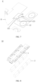
- FIG. 1 is a schematic structural diagram (first perspective) of a circuit board sampling structure according to some embodiments of this application
- FIG. 2 is a schematic structural diagram (second perspective) of a circuit board sampling structure according to some embodiments of this application
- FIG. 3 is an enlarged schematic view (second perspective) of zone A of a circuit board sampling structure according to some embodiments of this application
- FIG. 4 is a schematic structural diagram (third perspective) of a circuit board sampling structure according to some embodiments of this application
- FIG. 5 is an enlarged schematic view (third perspective) of zone B of a circuit board sampling structure according to some embodiments of this application
- FIG. 1 is a schematic structural diagram (first perspective) of a circuit board sampling structure according to some embodiments of this application
- FIG. 2 is a schematic structural diagram (second perspective) of a circuit board sampling structure according to some embodiments of this application
- FIG. 3 is an enlarged schematic view (second perspective) of zone A of a circuit board sampling structure according to some embodiments of this application
- FIG. 4 is
- FIG. 6 is a schematic structural diagram (fourth perspective) of a circuit board sampling structure in an exploded state according to some embodiments of this application
- FIG. 7 is an enlarged schematic view (fourth perspective) of zone C of a circuit board sampling structure in an exploded state according to some embodiments of this application
- FIG. 8 is a schematic structural diagram of a battery module in an exploded state according to some embodiments of this application.
- This application provides a circuit board sampling structure 1.
- the circuit board sampling structure 1 includes a circuit board 11, busbars 12, and connectors 13.
- An edge of the circuit board 11 is extended with connecting arms 111, the busbar 12 is provided with at least one plug hole 121, and a side of the connector 13 is provided with at least one plug part 131, where the plug part 131 is plugged in the plug hole 121, and an end of the connecting arm 111 away from the circuit board 11 is clamped between the connector 13 and the busbar 12.
- a sampling and detection circuit is provided in the circuit board 11, where the sampling and detection circuit has sampling and detection functions, such as voltage sampling and temperature sampling.
- the circuit board 11 may be in a linear shape extending along the first direction as shown in FIG. 1 , may be in a crossed shape, or may be in other shapes. This is not specifically limited herein.
- An edge of the circuit board 11 is extended with connecting arms 111, where a circuit is provided in the connecting arm 111, and the circuit is connected to the sampling and detection circuit in the circuit board 11.
- the edge of the circuit board 11 may be the edge extending along the first direction as shown in FIG. 1 , or may be another edge.
- the foregoing circuit board 11 may have multiple connecting arms 111 extending from one edge or may have multiple connecting arms 111 extending from multiple edges.
- the busbar 12 is used for implementing series or parallel connection between multiple battery cells 2 in the battery module 10.
- the busbar 12 is provided with at least one plug hole 121, where a shape of the plug hole 121 may be rectangle, triangle, trapezoid, or other shapes.
- the plug part 131 of the connector 13 is used for inserting into the plug hole 121 of the busbar 12, so that an end of the connecting arm 111 away from the circuit board 11 can be clamped between the connector 13 and the busbar 12, thereby reducing probability of relative replacement between the connecting arm 111 and the busbar 12 during connection.
- the connector 13 and the plug part 131 on one side thereof may be metal sheet made of aluminum, copper, nickel, and the like. This can improve strength of the connector 13 and the plug part 131 on one side thereof, so as to reduce probability of cracks of the connector 13 and the plug part 131.
- the plug part 131 may extend obliquely from one side of the connector 13, or may extend vertically.
- the connecting arm 111 and the busbar 12 are electrically connected.
- the connecting arm 111 and the busbar 12 each are provided with an electrical contact point on their respective surfaces in contact with each other.
- the electrical contact point of the connecting arm 111 contacts the electrical contact point of the busbar 12, so as to implement electrical connection between the connecting arm 111 and the busbar 12.
- the connecting arm 111 is welded to the busbar 12 to implement electrical connection between the connecting arm 111 and the busbar 12.
- the circuit board 11 of the circuit board sampling structure 1 are provided with four connecting arms 111 on both sides in the first direction, where each connecting arm 111 is clamped between one connector 13 and one busbar 12 at an end away from the circuit board 11.
- a part of the plug part 131 may be first inserted into the plug hole 121, the end of the connecting arm 111 away from the end of the circuit board 11 is disposed between the connector 13 and the busbar 12, the end edge of the connecting arm 111 away from the circuit board 11 abuts against the plug part 131, and then insertion of the plug part 131 proceeds until two end surfaces of the connecting arm 111 away from the circuit board 11 and facing away from each other are each fitted against the connector 13 and the busbar 12.
- the circuit board 11 When each busbar 12 is connected to a battery cell 2, the circuit board 11 is connected to eight battery cells 2, where the eight battery cells 2 are connected in series or parallel with each other, and the sampling and detection circuit in the circuit board 11 can sample and detect information such as voltage and temperature of the battery cells 2.
- the connecting arm 111 and the busbar 12 can be pre-fixed before the electrical connection by using the connector 13, reducing the probability of relative movement during performing electrical connection between the connecting arm 111 and the busbar 12, thereby improving the assembly efficiency between the circuit board 11 and the busbar 12.
- the connecting arm 111 and the busbar 12 are electrically connected, so that the connecting arm 111 and the busbar 12 can be electrically connected toout using a sampling connection piece, thereby improving the assembly efficiency and reducing the production cost of the circuit board sampling structure 1.
- the connector 13 enables one end of the connecting arm 111 away from the circuit board 11 to be clamped between the connector 13 and the busbar 12, thereby improving structural strength when the connecting arm 111 and the busbar 12 are connected.
- the plug part 131 and the busbar 12 are snap-fitted.
- the plug part 131 and the busbar 12 are snap-fitted, that is, the plug part 131 is provided with a first snapping portion adapted to the first snapping portion, the busbar 12 is provided with a second snapping portion.
- a snap-fit of the first snapping portion and the second snapping portion can indicate that the plug part 131 and the busbar 12 are snap-fitted.
- the first snapping portion and the second snapping portion can not only cooperate with each other to snap-fit, but also can separate from each other to separate the plug part 131 from the busbar 12.
- the plug part 131 and the busbar 12 are snap-fitted, so as to improve structural strength when the plug part 131 and the busbar 12 are connected, and reduce the probability of the connector 13 detaching from the busbar 12.
- an end of the plug part 131 away from the connector 13 is bent with a hook portion 1311, where the hook portion 1311 is hooked on the surface of the busbar 12 away from connecting arm 111.
- An end of the plug part 131 away from the connector 13 is bent with a hook portion 1311, where the hook portion 1311 is hooked on the surface of the busbar 12 away from connecting arm 111, that is, the plug part 131 can penetrate through the plug hole 121 on the surface of one side of the busbar 12 and make the hook portion 1311 be located on another side of the busbar 12, where the hook portion 1311 is hooked on the surface of the busbar 12 away from connecting arm 111.
- a distance between the hook portion 1311 and the connector 13 is greater than or equal to thickness of the busbar 12. In order to improve structural strength when the plug part 131 and the busbar 12 are connected, the distance between the hook portion 1311 and the connector 13 is equal to thickness of the busbar 12.
- the hook portion 1311 may be one portion of the plug part 131.
- the plug part 131 extends vertically along one side of the connector 13, and the hook portion 1311 is formed by bending an end of the plug part 131 away from the connector 13.
- a side of the busbar 12 away from the connecting arm 111 is disposed with an assembly tool, where surface of the assembly tool facing the busbar 12 is recessed with a recess portion, and the end of the plug part 131 away from the connector 13 passes through the plug hole 121 on one side of the busbar 12 and is located on another side of the busbar 12, and bends against the recess portion of the assembly tool, so as to form the hook portion 1311.
- the recess portion may be a recessed arc surface.
- the hook portion 1311 is hooked on the surface of the busbar 12 away from the connecting arm 111, thereby reducing the possibility of the plug part 131 detaching from the plug hole 121, and the connector 13 is simple in structure and easy to prepare.
- the plug hole 121 is provided in multiple, and the multiple plug holes 121 may include two plug holes 121 spaced apart or two plug holes 121 arranged closely.
- One plug hole 121 is inserted with at least one plug part 131, meaning that one plug hole 121 is inserted with one plug part 131 or multiple plug parts 131.
- the multiple plug holes 121 are provided to accommodate multiple plug parts 131, resulting in a relatively high structural strength when the connector 13 and the busbar 12 are connected.
- FIG. 5 and FIG. 7 there are three plug holes 121, where the three plug holes 121 are arranged in a triangle.
- the end of the connecting arm 111 away from the circuit board 11 can be located between the three plug holes 121.
- the three plug holes 121 are arranged in a triangle, so that the end of the connecting arm 111 away from the circuit board 11 can be located between the three plug holes 121, thereby reducing the possibility that the end of the connecting arm 111 away from the circuit board 11 rotates relative to the busbar 12.
- the end of the connecting arm 111 away from the circuit board 11 is located in a zone defined by the multiple plug holes 121, and the end of the connecting arm 111 abuts against the plug part 131, thereby reducing the possibility that the end of the connecting arm 111 away from the circuit board 11 rotates relative to the busbar 12.
- the connecting arm 111 and the busbar 12 are welded.
- the connecting arm 111 and the busbar 12 may be laser welded or ultrasonic welded. When the connecting arm 111 and the busbar 12 are welded, the connecting arm 111 and the busbar 12 are electrically connected, so that the busbar 12, the connecting arm 111, and the circuit board 11 form a signal sampling circuit.
- welding can not only achieve an electrical connection between the connecting arm 111 and the busbar 12, but also result in a relatively high structural strength when the connecting arm 111 and the busbar 12 are connected.
- At least a portion of the connecting arm 111 is in a bent shape.
- At least a portion of the connecting arm 111 is in a bent shape, meaning that the connecting arm 111 is entirely or locally bent.
- At least a portion of the connecting arm 111 is in a bent shape, meaning that at least a portion of the connecting arm 111 is not straight.
- a portion of the connecting arm 111 is in a fold-line shape.
- a portion of connecting arms 111 are in a wave shape.
- Bent connecting arms 111 can deform, where deforming includes but is not limited to the following types: being partially prolonged, being partially shortened, and being partially bulged.
- connecting arm 111 is in a bent shape, so that when the circuit board sampling structure 1 shakes, the bent portion of the connecting arm 111 can deform, thereby reducing possibility of damage to the circuit board sampling structure 1 caused by mutual pulling between the circuit board 11 and the busbar 12.
- edges of the circuit board 11 are provided with notches 112, where the connecting arm 111 extends from inside the notch 112 to the outside of the notch 112.
- the notches 112 can be formed by cutting the edge of the circuit board 11 or may be formed in other manners.
- the provision of the notches 112 can reduce material usage of the circuit board 11, thereby reducing the production cost of the circuit board sampling structure 1.
- the connecting arm 111 extends from inside the notch 112 to the outside of the notch 112, thereby reducing space occupation of the connecting arm 111.
- the notch 112 formed on the inner wall includes: a first inner wall 1121, where the first inner wall 1121 is perpendicular to an extension direction of the edge, the connecting arm 111 extends from the first inner wall 1121, and the connecting arm 111 bends in a direction perpendicular to the edge, the bent connecting arm 111 being in a bent shape.
- the notch 112 is provided on a first edge of the circuit board 11 extending along the first direction, where the first inner wall 1121 is perpendicular to the first edge, that is, the first inner wall 1121 is perpendicular to the first direction.
- the connecting arm 111 may be a portion of the circuit board 11.
- the circuit board 11 extends along the first direction
- the circuit board 11 is provided with multiple zones on both sides along the first direction.
- Each zone is formed by a first zone line, a second zone line, a third zone line, and a portion of the edge, where the first zone line and the second zone line are both perpendicular to the first direction
- the connecting arm 111 connected to the circuit board 11 can be formed by cutting along the third zone line and the second zone line.
- the cutting of the third zone line and the second zone line can be implemented by stamping.
- Such manner makes the connection between the connecting arm 111 and the circuit board 11 natural, with a low possibility of breakage.
- the first inner wall 1121 is perpendicular to the extension direction of the edge, and the connecting arm 111 extends from the first inner wall 1121 and bends towards the direction perpendicular to the edge, that is, the bent connecting arm 111 is parallel to the first inner wall 1121, thereby improving a visual effect of the circuit board sampling structure 1.
- this application provides a battery module 10, where the battery module 10 includes battery cells 2 and the circuit board sampling structure 1 according to any one of the following solutions, where the busbars 12 of the circuit board sampling structure 1 are connected to the battery cells 2.
- the battery cell 2 may be a secondary battery or a primary battery, a lithium-sulfur battery, a sodium-ion battery, or a magnesium-ion battery, without being limited thereto.
- the battery cell 2 may be cylindrical, flat, cuboid, or of other shapes.
- the battery module 10 there may be multiple battery cells 2, where the multiple battery cells 2 are electrically connected via the multiple busbars 12 of the circuit board sampling structure 1.
- the battery module 10 can be used without limitation in vehicles, ships, aircraft, and other electric devices.
- a power supply system of the electric device can be formed by using the battery module 10.
- the battery cells 2 are connected to the circuit board sampling structure 1, and the assembly efficiency of the circuit board sampling structure 1 is improved, thereby improving the assembly efficiency of the battery module 10.
- the battery module 10 may further include a first housing, where a cavity of the first housing is provided with the battery cells 2 and the circuit board sampling structure 1, thereby protecting the battery cells 2 and the circuit board sampling structure 1 via the first housing.
- this application further provides a battery pack 100, where the battery pack 100 includes the battery module 10 according to any one of the foregoing solutions.
- the battery pack 100 can be used without limitation in vehicles, ships, aircraft, and other electric devices.
- a power supply system of the electric device can be formed by using the battery pack 100.
- the battery modules 10 are provided in the battery pack 100, and the assembly efficiency of the battery module 10 is improved, thereby improving the assembly efficiency of the battery pack 100.
- the battery pack 100 may further include a second housing 20, where a cavity of the second housing 20 is provided with multiple battery modules 10.
- this application further provides an electric device 1000, where the electric device 1000 includes the battery pack 100 according to any one of the foregoing solutions.
- the electric device 1000 may include but is not limited to a mobile phone, a tablet, a laptop, an electric toy, an electric tool, an electric scooter, an electric vehicle, a ship, a spacecraft, or the like.
- the electric toy may include a fixed or mobile electric toy, for example, a game console, an electric toy car, an electric toy ship, and an electric toy airplane.
- the spacecraft may include an airplane, a rocket, a space shuttle, a spaceship, and the like.
- the battery pack 100 is provided in the electric device 1000, so that the improvement of assembly efficiency of the battery pack 100 can improve assembly efficiency of the electric device 1000.
- the electric device 1000 is a vehicle, and the vehicle 1000 may be a fossil fuel vehicle, a natural-gas vehicle, or a new energy vehicle, where the new energy vehicle may be a battery electric vehicle, a hybrid electric vehicle, a range-extended vehicle, or the like.
- the vehicle 1000 is provided with a battery pack 100 inside, where the battery pack 100 may be disposed at the bottom, front, or rear of the vehicle 1000.
- the battery pack 100 may be configured to power the vehicle 1000.
- the battery pack 100 may be used as an operational power source for the vehicle 1000.
- the vehicle 1000 may further include a controller and a motor, where the controller is configured to control the battery pack 100 to supply power to the motor, for example, to satisfy power needs of start, navigation, and driving of the vehicle 1000.
- the battery pack 100 can be used as not only the operational power source for the vehicle 1000 but also a driving power source for the vehicle 1000, replacing all or part of the fossil fuel or the natural gas to provide driving power for the vehicle 1000.
- a circuit board sampling structure 1 includes:
Landscapes
- Chemical & Material Sciences (AREA)
- Chemical Kinetics & Catalysis (AREA)
- Electrochemistry (AREA)
- General Chemical & Material Sciences (AREA)
- Engineering & Computer Science (AREA)
- Manufacturing & Machinery (AREA)
- Microelectronics & Electronic Packaging (AREA)
- Battery Mounting, Suspending (AREA)
- Connection Of Batteries Or Terminals (AREA)
Abstract
Description
- This application claims priority to
Chinese Patent Application No. 202220260030.6, filed with the China National Intellectual Property Administration on February 7, 2022 - Embodiments of this application relate to the battery field, and in particular, to a circuit board sampling structure, a battery module, a battery pack, and an electric device.
- Energy saving and emission reduction are crucial to the sustainable development of the automobile industry. Electric vehicles, with their advantages in energy conservation and emission reduction, have become an important part of sustainable development of the automobile industry. For electric vehicles, battery module technology is an important factor in connection with their development.
- Currently, the assembly efficiency of battery modules is low.
- In view of the foregoing problems, this application provides a circuit board sampling structure, a battery module, a battery pack, and an electric device, so as to alleviate the problem of low assembly efficiency of battery modules.
- According to a first aspect, this application provides a circuit board sampling structure, where the circuit board sampling structure includes: a circuit board, busbars, and connectors. An edge of the circuit board is extended with connecting arms, the busbar is provided with at least one plug hole, and a side of the connector is provided with at least one plug part, where the plug part is plugged in the plug hole, and an end of the connecting arm away from the circuit board is clamped between the connector and the busbar.
- In the technical solution in embodiments of this application, the connecting arm and the busbar can be pre-fixed before the electrical connection by using the connector, reducing the probability of relative movement during performing electrical connection between the connecting arm and the busbar, thereby improving the assembly efficiency between the circuit board and the busbar. In addition, when the end of the connecting arm away from the circuit board is clamped between the connector and the busbar, the connecting arm and the busbar are electrically connected, so that the connecting arm and the busbar can be electrically connected toout using a sampling connection piece, thereby improving the assembly efficiency and reducing the production cost of the circuit board sampling structure. In addition, the connector enables one end of the connecting arm away from the circuit board to be clamped between the connector and the busbar, thereby improving structural strength when the connecting arm and the busbar are connected.
- In some embodiments, the plug part and the busbar are snap-fitted. The plug part and the busbar are snap-fitted, which can improve structural strength when the plug part and the busbar are connected, and reduce the probability of the connector detaching from the busbar.
- In some embodiments, an end of the plug part away from the connector is bent with a hook portion, and the hook portion is hooked on the surface of the busbar away from the connecting arm. The hook portion is hooked on the surface of the busbar away from the connecting arm, which can reduce the possibility of the plug part detaching from the plug hole, and the connector is simple in structure and easy to prepare.
- In some embodiments, there are multiple plug holes, one plug hole being plugged with at least one plug part. The multiple plug holes are provided to accommodate multiple plug parts, resulting in a relatively high structural strength when the connector and the busbar are connected.
- In some embodiments, there are three plug holes, the three plug holes being distributed in a triangle. The three plug holes are arranged in a triangle, so that the end of the connecting arm away from the circuit board can be located between the three plug holes, thereby reducing the possibility that the end of the connecting arm away from the circuit board rotates relative to the busbar.
- In some embodiments, the end of the connecting arm away from the circuit board is located in a zone defined by the multiple plug holes, and the edge of the connecting arm abuts against the plug part. This can reduce possibility that the end of the connecting arm away from the circuit board rotates relative to the busbar.
- In some embodiments, the connecting arm and the busbar are welded. Welding can not only achieve an electrical connection between the connecting arm and the busbar, but also result in a relatively high structural strength when the connecting arm and the busbar are connected.
- In some embodiments, at least a portion of the connecting arm is in a bent shape. At least a portion of the connecting arm is in a bent shape, so that when the circuit board sampling structure shakes, the bent portion of the connecting arm can deform, thereby reducing possibility of damage to the circuit board sampling structure caused by mutual pulling between the circuit board and the busbar.
- In some embodiments, an edge of the circuit board is provided with notches, and the connecting arm extends from inside the notch to the outside of the notch. The provision of the notches can reduce material usage of the circuit board, thereby reducing the production cost of the circuit board sampling structure. The connecting arm extends from inside the notch to the outside of the notch, thereby reducing space occupation of the connecting arm.
- In some embodiments, an inner wall forming the notch includes: a first inner wall, where the first inner wall is perpendicular to an extension direction of the edge, the connecting arm extends from the first inner wall, and the connecting arm bends in a direction perpendicular to the edge, where the bent connecting arm is in a bent shape. The first inner wall is perpendicular to the extension direction of the edge, and the connecting arm extends from the first inner wall and bends towards the direction perpendicular to the edge; that is, the bent connecting arm is parallel to the first inner wall, thereby improving the visual effect of the circuit board sampling structure.
- According to a second aspect, this application provides a battery module, where the battery module includes battery cells and the circuit board sampling structure according to any one of the first aspect, and busbars of the circuit board sampling structure are connected to the battery cells. The battery cells are connected to the circuit board sampling structure, and the assembly efficiency of the circuit board sampling structure is improved, thereby improving the assembly efficiency of the battery module.
- According to a third aspect, this application provides a battery pack, where the battery pack includes the battery modules according to the second aspect. The battery modules are provided in the battery pack, and the assembly efficiency of the battery module is improved, thereby improving the assembly efficiency of the battery pack.
- According to a fourth aspect, this application provides an electric device, where the electric device includes the battery pack according to the third aspect. The battery pack is provided in the electric device, and the assembly efficiency of the battery pack is improved, thereby improving the assembly efficiency of the electric device.
- The foregoing description is merely an overview of the technical solution of this application. For a clear understanding of the technical means in this application such that they can be implemented according to the content of the specification, and to make the above and other objectives, features and advantages of this application obvious and easy to understand, the following describes specific embodiments of this application.
- Persons of ordinary skill in the art can clearly understand various other advantages and benefits by reading the detailed description of the preferred embodiments below. The accompanying drawings are merely intended to illustrate the preferred embodiments and are not intended to limit this application. In addition, in all the accompanying drawings, like reference signs denote like components. In the accompanying drawings:
-
FIG. 1 is a schematic structural diagram (first perspective) of a circuit board sampling structure according to some embodiments of this application; -
FIG. 2 is a schematic structural diagram (second perspective) of a circuit board sampling structure according to some embodiments of this application; -
FIG. 3 is an enlarged schematic view (second perspective) of zone A of a circuit board sampling structure according to some embodiments of this application; -
FIG. 4 is a schematic structural diagram (third perspective) of a circuit board sampling structure according to some embodiments of this application; -
FIG. 5 is an enlarged schematic view (third perspective) of zone B of a circuit board sampling structure according to some embodiments of this application; -
FIG. 6 is a schematic structural diagram (fourth perspective) of a circuit board sampling structure in an exploded state according to some embodiments of this application; -
FIG. 7 is an enlarged schematic view (fourth perspective) of zone C of a circuit board sampling structure in an exploded state according to some embodiments of this application; -
FIG. 8 is a schematic structural diagram of a battery module in an exploded state according to some embodiments of this application; -
FIG. 9 is a schematic structural diagram of a battery pack according to some embodiments of this application; and -
FIG. 10 is a schematic structural diagram of an electric device according to some embodiments of this application. - Reference signs in specific embodiments are as follows:
- 1. circuit board sampling structure, 11. circuit board, 111. connecting arm, 112. notch, 1121. first inner wall, 12. busbar, 121. plug hole, 13. connector, 131. plug part, 1311. hook portion;
- 2. battery cell;
- 10. battery module;
- 20. second housing;
- 100. battery pack; and
- 1000. electric device.
- The following describes in detail the embodiments of technical solutions of this application with reference to the accompanying drawings. The following embodiments are merely intended for a clear description of the technical solutions of this application and therefore are merely used as examples which do not constitute any limitations on the protection scope of this application.
- Unless otherwise defined, all technical and scientific terms used herein shall have the same meanings as commonly understood by persons skilled in the art to which this application relates. The terms used herein are intended to merely describe the specific embodiments rather than to limit this application. The terms "include", "comprise", and "have" and any other variations thereof in the specification, claims and brief description of drawings of this application are intended to cover non-exclusive inclusions.
- In the description of the embodiments of this application, the terms "first", "second" and the like are merely intended to distinguish between different objects, and shall not be understood as any indication or implication of relative importance or any implicit indication of the number, particular sequence or primary-secondary relationship of the technical features indicated. In the description of the embodiments of this application, "multiple" means at least two unless otherwise specifically stated.
- In this specification, reference to "embodiment" means that specific features, structures or characteristics described with reference to the embodiment may be incorporated in at least one embodiment of this application. The word "embodiment" appearing in various places in the specification does not necessarily refer to the same embodiment or an independent or alternative embodiment that is exclusive of other embodiments. It is explicitly or implicitly understood by persons skilled in the art that the embodiments described herein may be combined with other embodiments.
- In the description of the embodiments of this application, the term "and/or" is only an associative relationship for describing associated objects, indicating that three relationships may be present. For example, A and/or B may indicate the following three cases: presence of A, presence of both A and B, and presence of B. In addition, the character "/" in this specification generally indicates an "or" relationship between the contextually associated objects.
- In the description of the embodiments of this application, the term "multiple" means more than two (inclusive). Similarly, "multiple groups" means more than two (inclusive) groups, and "multiple pieces" means more than two (inclusive) pieces.
- In the description of the embodiments of this application, the orientations or positional relationships indicated by the technical terms "center", "longitudinal", "transverse", "length", "width", "thickness", "upper", "lower", "front", "rear", "left", "right", "vertical", "horizontal", "top", "bottom", "inside", "outside", "clockwise", "counterclockwise", "axial", "radial", "circumferential", and the like are based on the orientations or positional relationships as shown in the accompanying drawings. These terms are merely for the ease and brevity of description of the embodiments of this application rather than indicating or implying that the apparatuses or components mentioned must have specific orientations or must be constructed or manipulated according to specific orientations, and therefore shall not be construed as any limitations on the embodiments of this application.
- In the description of the embodiments of this application, unless otherwise specified and defined explicitly, the terms "mount", "connect", "join", and "fasten" should be understood in their general senses. For example, they may refer to a fixed connection, a detachable connection, or an integral connection, may refer to a mechanical connection or an electrical connection, and may refer to a direct connection, an indirect connection via an intermediate medium, an internal communication between two elements, or an interaction between two elements. Persons of ordinary skill in the art can understand specific meanings of these terms in this application as appropriate to specific situations.
- Currently, from a perspective of market development, application of traction batteries is being more extensive. Traction batteries have been not only used in energy storage power supply systems such as hydroelectric power plants, thermal power plants, wind power plants, and solar power plants, but also widely used in many other fields including electric transportation tools such as electric bicycles, electric motorcycles, and electric vehicles, military equipment, and aerospace. With the continuous expansion of application fields of traction batteries, market demands for the traction batteries are also expanding.
- The inventors have noted that a battery module is provided with busbars and a circuit board, where the busbars are configured to connect battery cells, connecting arms of the circuit board are connected to the busbars, and the circuit board can sample and detect information such as voltage and temperature on the battery cells connected to the busbars via the connecting arm and the busbars. However, when the connecting arms and the busbars of the circuit board are electrically connected, relative displacement therebetween is easy to occur, causing low assembly efficiency of the battery module. In this case, being electrically connected means that the transmission of electrical signals can be performed between the connecting arms and the busbars.
- In order to alleviate the problem of low assembly efficiency of the battery module, the applicant has found through research that before connections of the connecting arms with the busbars, the connecting arms can be limited at positions on the busbars at which corresponding connecting arms are connected. In this way, when the connecting arms and the busbars are in electrical connection, relative displacement therebetween does not occur, thereby improving the assembly efficiency of the battery module.
- In view of this, in order to alleviate the problem of low assembly efficiency of the battery module, the inventors have designed, through deep research, a circuit board sampling structure. The connectors are used to limit the connecting arms at positions on the busbars at which corresponding connecting arms are connected, so that during electrical connection of the connecting arms and the busbars, when relative displacement therebetween occurs, the connector can limit the movement of the connecting arm relative to the busbar.
- According to some embodiments in this application, referring to
FIG. 1 and with reference toFIG. 2 to FIG. 8 ,FIG. 1 is a schematic structural diagram (first perspective) of a circuit board sampling structure according to some embodiments of this application,FIG. 2 is a schematic structural diagram (second perspective) of a circuit board sampling structure according to some embodiments of this application,FIG. 3 is an enlarged schematic view (second perspective) of zone A of a circuit board sampling structure according to some embodiments of this application,FIG. 4 is a schematic structural diagram (third perspective) of a circuit board sampling structure according to some embodiments of this application,FIG. 5 is an enlarged schematic view (third perspective) of zone B of a circuit board sampling structure according to some embodiments of this application,FIG. 6 is a schematic structural diagram (fourth perspective) of a circuit board sampling structure in an exploded state according to some embodiments of this application,FIG. 7 is an enlarged schematic view (fourth perspective) of zone C of a circuit board sampling structure in an exploded state according to some embodiments of this application, andFIG. 8 is a schematic structural diagram of a battery module in an exploded state according to some embodiments of this application. This application provides a circuitboard sampling structure 1. The circuitboard sampling structure 1 includes acircuit board 11,busbars 12, andconnectors 13. An edge of thecircuit board 11 is extended with connectingarms 111, thebusbar 12 is provided with at least oneplug hole 121, and a side of theconnector 13 is provided with at least oneplug part 131, where theplug part 131 is plugged in theplug hole 121, and an end of the connectingarm 111 away from thecircuit board 11 is clamped between theconnector 13 and thebusbar 12. - A sampling and detection circuit is provided in the
circuit board 11, where the sampling and detection circuit has sampling and detection functions, such as voltage sampling and temperature sampling. - The
circuit board 11 may be in a linear shape extending along the first direction as shown inFIG. 1 , may be in a crossed shape, or may be in other shapes. This is not specifically limited herein. - An edge of the
circuit board 11 is extended with connectingarms 111, where a circuit is provided in the connectingarm 111, and the circuit is connected to the sampling and detection circuit in thecircuit board 11. The edge of thecircuit board 11 may be the edge extending along the first direction as shown inFIG. 1 , or may be another edge. The foregoingcircuit board 11 may have multiple connectingarms 111 extending from one edge or may have multiple connectingarms 111 extending from multiple edges. - The
busbar 12 is used for implementing series or parallel connection betweenmultiple battery cells 2 in thebattery module 10. - The
busbar 12 is provided with at least oneplug hole 121, where a shape of theplug hole 121 may be rectangle, triangle, trapezoid, or other shapes. - The
plug part 131 of theconnector 13 is used for inserting into theplug hole 121 of thebusbar 12, so that an end of the connectingarm 111 away from thecircuit board 11 can be clamped between theconnector 13 and thebusbar 12, thereby reducing probability of relative replacement between the connectingarm 111 and thebusbar 12 during connection. - The
connector 13 and theplug part 131 on one side thereof may be metal sheet made of aluminum, copper, nickel, and the like. This can improve strength of theconnector 13 and theplug part 131 on one side thereof, so as to reduce probability of cracks of theconnector 13 and theplug part 131. - The
plug part 131 may extend obliquely from one side of theconnector 13, or may extend vertically. - When the end of the connecting
arm 111 away from thecircuit board 11 is clamped between theconnector 13 and thebusbar 12, the connectingarm 111 and thebusbar 12 are electrically connected. For example, the connectingarm 111 and thebusbar 12 each are provided with an electrical contact point on their respective surfaces in contact with each other. When one end of the connectingarm 111 away from thecircuit board 11 is clamped between theconnector 13 and thebusbar 12, the electrical contact point of the connectingarm 111 contacts the electrical contact point of thebusbar 12, so as to implement electrical connection between the connectingarm 111 and thebusbar 12. For another example, when one end of the connectingarm 111 away from thecircuit board 11 is clamped between theconnector 13 and thebusbar 12, the connectingarm 111 is welded to thebusbar 12 to implement electrical connection between the connectingarm 111 and thebusbar 12. - In one embodiment, as shown in
FIG. 1 , thecircuit board 11 of the circuitboard sampling structure 1 are provided with four connectingarms 111 on both sides in the first direction, where each connectingarm 111 is clamped between oneconnector 13 and onebusbar 12 at an end away from thecircuit board 11. In implementation, a part of theplug part 131 may be first inserted into theplug hole 121, the end of the connectingarm 111 away from the end of thecircuit board 11 is disposed between theconnector 13 and thebusbar 12, the end edge of the connectingarm 111 away from thecircuit board 11 abuts against theplug part 131, and then insertion of theplug part 131 proceeds until two end surfaces of the connectingarm 111 away from thecircuit board 11 and facing away from each other are each fitted against theconnector 13 and thebusbar 12. When eachbusbar 12 is connected to abattery cell 2, thecircuit board 11 is connected to eightbattery cells 2, where the eightbattery cells 2 are connected in series or parallel with each other, and the sampling and detection circuit in thecircuit board 11 can sample and detect information such as voltage and temperature of thebattery cells 2. - In this embodiment, the connecting
arm 111 and thebusbar 12 can be pre-fixed before the electrical connection by using theconnector 13, reducing the probability of relative movement during performing electrical connection between the connectingarm 111 and thebusbar 12, thereby improving the assembly efficiency between thecircuit board 11 and thebusbar 12. In addition, when the end of the connectingarm 111 away from thecircuit board 11 is clamped between theconnector 13 and thebusbar 12, the connectingarm 111 and thebusbar 12 are electrically connected, so that the connectingarm 111 and thebusbar 12 can be electrically connected toout using a sampling connection piece, thereby improving the assembly efficiency and reducing the production cost of the circuitboard sampling structure 1. In addition, theconnector 13 enables one end of the connectingarm 111 away from thecircuit board 11 to be clamped between theconnector 13 and thebusbar 12, thereby improving structural strength when the connectingarm 111 and thebusbar 12 are connected. - According to some embodiments in this application, referring to
FIG. 1 to FIG. 7 , theplug part 131 and thebusbar 12 are snap-fitted. - The
plug part 131 and thebusbar 12 are snap-fitted, that is, theplug part 131 is provided with a first snapping portion adapted to the first snapping portion, thebusbar 12 is provided with a second snapping portion. A snap-fit of the first snapping portion and the second snapping portion can indicate that theplug part 131 and thebusbar 12 are snap-fitted. - The first snapping portion and the second snapping portion can not only cooperate with each other to snap-fit, but also can separate from each other to separate the
plug part 131 from thebusbar 12. - In this embodiment, the
plug part 131 and thebusbar 12 are snap-fitted, so as to improve structural strength when theplug part 131 and thebusbar 12 are connected, and reduce the probability of theconnector 13 detaching from thebusbar 12. - According to some embodiments in this application, referring to
FIG. 4 andFIG. 5 , an end of theplug part 131 away from theconnector 13 is bent with ahook portion 1311, where thehook portion 1311 is hooked on the surface of thebusbar 12 away from connectingarm 111. - An end of the
plug part 131 away from theconnector 13 is bent with ahook portion 1311, where thehook portion 1311 is hooked on the surface of thebusbar 12 away from connectingarm 111, that is, theplug part 131 can penetrate through theplug hole 121 on the surface of one side of thebusbar 12 and make thehook portion 1311 be located on another side of thebusbar 12, where thehook portion 1311 is hooked on the surface of thebusbar 12 away from connectingarm 111. Herein, a distance between thehook portion 1311 and theconnector 13 is greater than or equal to thickness of thebusbar 12. In order to improve structural strength when theplug part 131 and thebusbar 12 are connected, the distance between thehook portion 1311 and theconnector 13 is equal to thickness of thebusbar 12. - The
hook portion 1311 may be one portion of theplug part 131. For example, theplug part 131 extends vertically along one side of theconnector 13, and thehook portion 1311 is formed by bending an end of theplug part 131 away from theconnector 13. In implementation, a side of thebusbar 12 away from the connectingarm 111 is disposed with an assembly tool, where surface of the assembly tool facing thebusbar 12 is recessed with a recess portion, and the end of theplug part 131 away from theconnector 13 passes through theplug hole 121 on one side of thebusbar 12 and is located on another side of thebusbar 12, and bends against the recess portion of the assembly tool, so as to form thehook portion 1311. Herein, the recess portion may be a recessed arc surface. - In this embodiment, the
hook portion 1311 is hooked on the surface of thebusbar 12 away from the connectingarm 111, thereby reducing the possibility of theplug part 131 detaching from theplug hole 121, and theconnector 13 is simple in structure and easy to prepare. - According to some embodiments in this application, referring to
FIG. 5 andFIG. 7 , there are multiple plug holes 121, where oneplug hole 121 is inserted with at least oneplug part 131. - The
plug hole 121 is provided in multiple, and the multiple plug holes 121 may include twoplug holes 121 spaced apart or twoplug holes 121 arranged closely. - One
plug hole 121 is inserted with at least oneplug part 131, meaning that oneplug hole 121 is inserted with oneplug part 131 ormultiple plug parts 131. - In this embodiment, the multiple plug holes 121 are provided to accommodate
multiple plug parts 131, resulting in a relatively high structural strength when theconnector 13 and thebusbar 12 are connected. - According to some embodiments in this application, referring to
FIG. 5 andFIG. 7 , there are threeplug holes 121, where the threeplug holes 121 are arranged in a triangle. - During use, the end of the connecting
arm 111 away from thecircuit board 11 can be located between the three plug holes 121. - In this embodiment, the three
plug holes 121 are arranged in a triangle, so that the end of the connectingarm 111 away from thecircuit board 11 can be located between the threeplug holes 121, thereby reducing the possibility that the end of the connectingarm 111 away from thecircuit board 11 rotates relative to thebusbar 12. - According to some embodiments in this application, referring to
FIG. 7 , the end of the connectingarm 111 away from thecircuit board 11 is located in a zone defined by the multiple plug holes 121, and the end of the connectingarm 111 abuts against theplug part 131, thereby reducing the possibility that the end of the connectingarm 111 away from thecircuit board 11 rotates relative to thebusbar 12. - According to some embodiments in this application, the connecting
arm 111 and thebusbar 12 are welded. - The connecting
arm 111 and thebusbar 12 may be laser welded or ultrasonic welded. When the connectingarm 111 and thebusbar 12 are welded, the connectingarm 111 and thebusbar 12 are electrically connected, so that thebusbar 12, the connectingarm 111, and thecircuit board 11 form a signal sampling circuit. - In this embodiment, welding can not only achieve an electrical connection between the connecting
arm 111 and thebusbar 12, but also result in a relatively high structural strength when the connectingarm 111 and thebusbar 12 are connected. - According to some embodiments in this application, at least a portion of the connecting
arm 111 is in a bent shape. - At least a portion of the connecting
arm 111 is in a bent shape, meaning that the connectingarm 111 is entirely or locally bent. - At least a portion of the connecting
arm 111 is in a bent shape, meaning that at least a portion of the connectingarm 111 is not straight. For example, a portion of the connectingarm 111 is in a fold-line shape. For another example, a portion of connectingarms 111 are in a wave shape. -
Bent connecting arms 111 can deform, where deforming includes but is not limited to the following types: being partially prolonged, being partially shortened, and being partially bulged. - In this embodiment, at least a portion of connecting
arm 111 is in a bent shape, so that when the circuitboard sampling structure 1 shakes, the bent portion of the connectingarm 111 can deform, thereby reducing possibility of damage to the circuitboard sampling structure 1 caused by mutual pulling between thecircuit board 11 and thebusbar 12. - According to some embodiments in this application, referring to
FIG. 1 to FIG. 7 , edges of thecircuit board 11 are provided withnotches 112, where the connectingarm 111 extends from inside thenotch 112 to the outside of thenotch 112. - The
notches 112 can be formed by cutting the edge of thecircuit board 11 or may be formed in other manners. - In this embodiment, the provision of the
notches 112 can reduce material usage of thecircuit board 11, thereby reducing the production cost of the circuitboard sampling structure 1. The connectingarm 111 extends from inside thenotch 112 to the outside of thenotch 112, thereby reducing space occupation of the connectingarm 111. - According to some embodiments in this application, referring to
FIG. 2 andFIG. 3 , thenotch 112 formed on the inner wall includes: a firstinner wall 1121, where the firstinner wall 1121 is perpendicular to an extension direction of the edge, the connectingarm 111 extends from the firstinner wall 1121, and the connectingarm 111 bends in a direction perpendicular to the edge, the bent connectingarm 111 being in a bent shape. - For example, the
notch 112 is provided on a first edge of thecircuit board 11 extending along the first direction, where the firstinner wall 1121 is perpendicular to the first edge, that is, the firstinner wall 1121 is perpendicular to the first direction. - Herein, the connecting
arm 111 may be a portion of thecircuit board 11. For example, thecircuit board 11 extends along the first direction, thecircuit board 11 is provided with multiple zones on both sides along the first direction. Each zone is formed by a first zone line, a second zone line, a third zone line, and a portion of the edge, where the first zone line and the second zone line are both perpendicular to the first direction, and the connectingarm 111 connected to thecircuit board 11 can be formed by cutting along the third zone line and the second zone line. The cutting of the third zone line and the second zone line can be implemented by stamping. Such manner makes the connection between the connectingarm 111 and thecircuit board 11 natural, with a low possibility of breakage. - In this embodiment, the first
inner wall 1121 is perpendicular to the extension direction of the edge, and the connectingarm 111 extends from the firstinner wall 1121 and bends towards the direction perpendicular to the edge, that is, the bent connectingarm 111 is parallel to the firstinner wall 1121, thereby improving a visual effect of the circuitboard sampling structure 1. - According to some embodiments in this application, referring to
FIG. 8 , this application provides abattery module 10, where thebattery module 10 includesbattery cells 2 and the circuitboard sampling structure 1 according to any one of the following solutions, where thebusbars 12 of the circuitboard sampling structure 1 are connected to thebattery cells 2. - The
battery cell 2 may be a secondary battery or a primary battery, a lithium-sulfur battery, a sodium-ion battery, or a magnesium-ion battery, without being limited thereto. Thebattery cell 2 may be cylindrical, flat, cuboid, or of other shapes. - In the
battery module 10, there may bemultiple battery cells 2, where themultiple battery cells 2 are electrically connected via themultiple busbars 12 of the circuitboard sampling structure 1. - The
battery module 10 can be used without limitation in vehicles, ships, aircraft, and other electric devices. A power supply system of the electric device can be formed by using thebattery module 10. - In this embodiment, the
battery cells 2 are connected to the circuitboard sampling structure 1, and the assembly efficiency of the circuitboard sampling structure 1 is improved, thereby improving the assembly efficiency of thebattery module 10. - In some embodiments of this application, the
battery module 10 may further include a first housing, where a cavity of the first housing is provided with thebattery cells 2 and the circuitboard sampling structure 1, thereby protecting thebattery cells 2 and the circuitboard sampling structure 1 via the first housing. - According to some embodiments in this application, referring to
FIG. 9 , this application further provides abattery pack 100, where thebattery pack 100 includes thebattery module 10 according to any one of the foregoing solutions. - The
battery pack 100 can be used without limitation in vehicles, ships, aircraft, and other electric devices. A power supply system of the electric device can be formed by using thebattery pack 100. - In this embodiment, the
battery modules 10 are provided in thebattery pack 100, and the assembly efficiency of thebattery module 10 is improved, thereby improving the assembly efficiency of thebattery pack 100. - In some embodiments of this application, referring to
FIG. 9 , thebattery pack 100 may further include asecond housing 20, where a cavity of thesecond housing 20 is provided withmultiple battery modules 10. - According to some embodiments in this application, referring to
FIG. 10 , this application further provides anelectric device 1000, where theelectric device 1000 includes thebattery pack 100 according to any one of the foregoing solutions. - The
electric device 1000 may include but is not limited to a mobile phone, a tablet, a laptop, an electric toy, an electric tool, an electric scooter, an electric vehicle, a ship, a spacecraft, or the like. The electric toy may include a fixed or mobile electric toy, for example, a game console, an electric toy car, an electric toy ship, and an electric toy airplane. The spacecraft may include an airplane, a rocket, a space shuttle, a spaceship, and the like. - In this embodiment, the
battery pack 100 is provided in theelectric device 1000, so that the improvement of assembly efficiency of thebattery pack 100 can improve assembly efficiency of theelectric device 1000. - In some embodiments of this application, referring to
FIG. 10 , theelectric device 1000 is a vehicle, and thevehicle 1000 may be a fossil fuel vehicle, a natural-gas vehicle, or a new energy vehicle, where the new energy vehicle may be a battery electric vehicle, a hybrid electric vehicle, a range-extended vehicle, or the like. Thevehicle 1000 is provided with abattery pack 100 inside, where thebattery pack 100 may be disposed at the bottom, front, or rear of thevehicle 1000. Thebattery pack 100 may be configured to power thevehicle 1000. For example, thebattery pack 100 may be used as an operational power source for thevehicle 1000. Thevehicle 1000 may further include a controller and a motor, where the controller is configured to control thebattery pack 100 to supply power to the motor, for example, to satisfy power needs of start, navigation, and driving of thevehicle 1000. - In some embodiments of this application, the
battery pack 100 can be used as not only the operational power source for thevehicle 1000 but also a driving power source for thevehicle 1000, replacing all or part of the fossil fuel or the natural gas to provide driving power for thevehicle 1000. - In a specific embodiment, referring to
FIG. 1 to FIG. 7 , a circuitboard sampling structure 1 includes: - a
circuit board 11, where thecircuit board 11 is a rectangular board extending along a first direction, and fournotches 112 are provided on both sides of thecircuit board 11 in the first direction, and four connectingarms 111 corresponding to the fournotches 112 are respectively provided, where the connectingarm 111 is bent in a direction perpendicular to the first direction and is in a bent shape after bending; and the connectingarm 111 is formed by stamping a portion of an edge of thecircuit board 11; - eight
busbars 12, where eachbusbar 12 is provided with threeplug holes 121 arranged in a triangle; and - eight
connectors 13, where eachconnector 13 is provided with threeplug parts 131 arranged in a triangle on one side, the threeplug parts 131 of oneconnector 13 are respectively inserted into the threeplug holes 121 of onebusbar 12, and theplug part 131 passed through theplug hole 121 is bent and forms ahook portion 1311, where thehook portion 1311 abuts against surface of thebusbar 12 away from the connectingarm 111; - where an end portion of each connecting
arm 111 away from thecircuit board 11 is clamped between theconnected connector 13 andbusbar 12, each edge of the end portion of each connectingarm 111 away from thecircuit board 11 is located in corresponding threeplug parts 131 of theconnector 13 and abuts against the threeplug parts 131, and the end portion of the connectingarm 111 away from thecircuit board 11 and thebusbar 12 are welded. - In conclusion, it should be noted that the foregoing embodiments are for description of the technical solutions of this application only rather than for limiting this application. Although this application has been described in detail with reference to the foregoing embodiments, persons of ordinary skill in the art should appreciate that they can still make modifications to the technical solutions described in the embodiments or make equivalent replacements to some or all technical features thereof without departing from the scope of the technical solutions of the embodiments of this application. All such modifications and equivalent replacements shall fall within the scope of claims and specification of this application. In particular, as long as there is no structural conflict, the various technical features mentioned in the embodiments can be combined in any manner. This application is not limited to the specific embodiments disclosed in this specification but includes all technical solutions falling within the scope of the claims.
Claims (16)
- A circuit board sampling structure, comprising:a circuit board, wherein an edge of the circuit board is extended with a connecting arm;busbars, wherein the busbar is provided with at least one plug hole; andconnectors, wherein a side of the connector is provided with at least one plug part, the plug part is plugged in the plug hole, and an end of the connecting arm away from the circuit board is clamped between the connector and the busbar.
- The circuit board sampling structure according to claim 1, wherein
the plug part and the busbar are snap-fitted. - The circuit board sampling structure according to claim 2, wherein
an end of the plug part away from the connector is bent with a hook portion, and the hook portion is hooked on the surface of the busbar away from the connecting arm. - The circuit board sampling structure according to claim 3, wherein a distance between the hook portion and the connector is greater than or equal to thickness of the busbar.
- The circuit board sampling structure according to any one of claims 1 to 4, wherein
there are multiple plug holes, one plug hole being plugged with at least one plug part. - The circuit board sampling structure according to claim 5, wherein
there are three plug holes, the three plug holes being distributed in a triangle. - The circuit board sampling structure according to claim 5, wherein
the end of the connecting arm away from the circuit board is located in a zone defined by the multiple plug holes, and the edge of the connecting arm abuts against the plug part. - The circuit board sampling structure according to any one of claims 1 to 7, wherein
the connecting arm and the busbar are welded. - The circuit board sampling structure according to any one of claims 1 to 8, wherein
at least a portion of the connecting arm is in a bent shape. - The circuit board sampling structure according to claim 9, wherein
an edge of the circuit board is provided with notches, and the connecting arm extends from inside the notch to the outside of the notch. - The circuit board sampling structure according to claim 10, wherein
an inner wall forming the notch comprises: a first inner wall, wherein the first inner wall is perpendicular to an extension direction of the edge, the connecting arm extends from the first inner wall, and the connecting arm bends in a direction perpendicular to the edge, wherein the bent connecting arm is in a bent shape. - A battery module, comprising:battery cells; andthe circuit board sampling structure according to any one of claims 1 to 11, wherein busbars of the circuit board sampling structure are connected to the battery cells.
- The battery module according to claim 12, wherein the battery module further comprises:
a first housing, wherein a cavity of the first housing is provided with the battery cells and the circuit board sampling structure. - A battery pack, comprising:
the battery modules according to claim 12 or 13. - The battery pack according to claim 14, wherein the battery pack further comprises:
a second housing, wherein a cavity of the second housing is provided with multiple battery modules. - An electric device, comprising:
the battery pack according to claim 14 or 15.
Applications Claiming Priority (2)
| Application Number | Priority Date | Filing Date | Title |
|---|---|---|---|
| CN202220260030.6U CN216872203U (en) | 2022-02-07 | 2022-02-07 | Circuit board sampling structure, battery module, battery pack and electrical equipment |
| PCT/CN2023/074119 WO2023147771A1 (en) | 2022-02-07 | 2023-02-01 | Sampling structure with circuit board, and battery module, battery pack, and electric apparatus |
Publications (2)
| Publication Number | Publication Date |
|---|---|
| EP4407778A1 true EP4407778A1 (en) | 2024-07-31 |
| EP4407778A4 EP4407778A4 (en) | 2025-02-26 |
Family
ID=82155547
Family Applications (1)
| Application Number | Title | Priority Date | Filing Date |
|---|---|---|---|
| EP23749350.7A Pending EP4407778A4 (en) | 2022-02-07 | 2023-02-01 | Sampling structure with circuit board, and battery module, battery pack, and electric apparatus |
Country Status (6)
| Country | Link |
|---|---|
| US (1) | US20240297424A1 (en) |
| EP (1) | EP4407778A4 (en) |
| JP (1) | JP7801441B2 (en) |
| KR (1) | KR20240068736A (en) |
| CN (1) | CN216872203U (en) |
| WO (1) | WO2023147771A1 (en) |
Families Citing this family (2)
| Publication number | Priority date | Publication date | Assignee | Title |
|---|---|---|---|---|
| CN216872203U (en) * | 2022-02-07 | 2022-07-01 | 宁德时代新能源科技股份有限公司 | Circuit board sampling structure, battery module, battery pack and electrical equipment |
| CN120566023A (en) * | 2024-02-29 | 2025-08-29 | 宁德时代新能源科技股份有限公司 | Sampling circuit boards, batteries and power devices |
Family Cites Families (12)
| Publication number | Priority date | Publication date | Assignee | Title |
|---|---|---|---|---|
| JPS5736817Y2 (en) * | 1977-09-30 | 1982-08-13 | ||
| JPS5881804U (en) * | 1981-11-28 | 1983-06-02 | 松下電工株式会社 | Louver |
| JP6581959B2 (en) * | 2016-12-19 | 2019-09-25 | 矢崎総業株式会社 | Conductor module for terminals |
| RS61814B1 (en) * | 2016-12-27 | 2021-06-30 | Yura Corporation Co Ltd | Flexible circuit board and frame assembly including same |
| CN110752340B (en) * | 2018-07-23 | 2021-02-09 | 宁德时代新能源科技股份有限公司 | Sampling components and battery modules |
| CN109301143B (en) * | 2018-10-19 | 2024-04-19 | 胜蓝科技股份有限公司 | Integrated anti-tearing automobile battery sampling wire harness |
| JP7212504B2 (en) * | 2018-11-22 | 2023-01-25 | 株式会社オートネットワーク技術研究所 | connection module |
| CN209730082U (en) * | 2019-01-30 | 2019-12-03 | 宁德时代新能源科技股份有限公司 | Sampling circuit board and battery module |
| CN110112477B (en) * | 2019-05-20 | 2024-02-23 | 安费诺(常州)连接系统有限公司 | Battery cell connection system |
| CN210467965U (en) * | 2019-09-23 | 2020-05-05 | 宁德时代新能源科技股份有限公司 | Battery modules, battery packs and vehicles |
| CN213184480U (en) * | 2020-10-27 | 2021-05-11 | 远景动力技术(江苏)有限公司 | Battery pack and battery module |
| CN216872203U (en) * | 2022-02-07 | 2022-07-01 | 宁德时代新能源科技股份有限公司 | Circuit board sampling structure, battery module, battery pack and electrical equipment |
-
2022
- 2022-02-07 CN CN202220260030.6U patent/CN216872203U/en active Active
-
2023
- 2023-02-01 EP EP23749350.7A patent/EP4407778A4/en active Pending
- 2023-02-01 JP JP2024524495A patent/JP7801441B2/en active Active
- 2023-02-01 KR KR1020247014105A patent/KR20240068736A/en active Pending
- 2023-02-01 WO PCT/CN2023/074119 patent/WO2023147771A1/en not_active Ceased
-
2024
- 2024-04-25 US US18/646,745 patent/US20240297424A1/en active Pending
Also Published As
| Publication number | Publication date |
|---|---|
| WO2023147771A1 (en) | 2023-08-10 |
| JP2024541004A (en) | 2024-11-06 |
| EP4407778A4 (en) | 2025-02-26 |
| JP7801441B2 (en) | 2026-01-16 |
| KR20240068736A (en) | 2024-05-17 |
| US20240297424A1 (en) | 2024-09-05 |
| CN216872203U (en) | 2022-07-01 |
Similar Documents
| Publication | Publication Date | Title |
|---|---|---|
| US20240297424A1 (en) | Circuit board sampling structure, battery module, battery pack, and electric device | |
| EP4513629A1 (en) | Thermal management component, battery, and electric device | |
| CN216903165U (en) | Flexible circuit board assembly, battery and electric device | |
| CN216015582U (en) | Battery box, battery and electrical device | |
| EP4462583A1 (en) | Battery cell and manufacturing method therefor, battery, and power consuming device | |
| EP4358174A1 (en) | Electrode sheet, electrode assembly, battery cell, battery and electric apparatus | |
| EP4456298A1 (en) | Battery top cover, top cover assembly, battery cell, battery, and electric device | |
| CN218548747U (en) | Insulating film, battery and electric device | |
| CN221928491U (en) | Battery components, battery packs and electrical equipment | |
| US20260074375A1 (en) | Battery cell, battery, and power consuming apparatus | |
| WO2023165376A1 (en) | Sampling assembly, battery, and electric device | |
| US20250183490A1 (en) | Connecting terminal, battery, and electrical device | |
| EP4685984A1 (en) | Battery cell, battery, and electric device | |
| EP4507041A1 (en) | Battery cell, battery and electric device | |
| CN217507575U (en) | Battery connector group, battery and electric device | |
| EP4231369A1 (en) | Mounting apparatus, battery, power apparatus, battery manufacturing method, and manufacturing device | |
| CN221427943U (en) | Batteries and electrical devices | |
| CN220731678U (en) | Battery module, battery and power consumption device | |
| CN221057486U (en) | Battery cable connector protection device, battery and power-consuming device | |
| CN222776510U (en) | Battery circuit board positioning device, crimping device and battery production system | |
| CN221201468U (en) | Batteries, electrical connectors and electrical devices | |
| CN220692269U (en) | Batteries and electrical devices | |
| EP4503221A1 (en) | End cover assembly, battery cell, battery, and electrical apparatus | |
| CN222507905U (en) | Battery and electricity utilization device | |
| CN222088805U (en) | Battery cell, battery and electricity utilization device |
Legal Events
| Date | Code | Title | Description |
|---|---|---|---|
| STAA | Information on the status of an ep patent application or granted ep patent |
Free format text: STATUS: THE INTERNATIONAL PUBLICATION HAS BEEN MADE |
|
| PUAI | Public reference made under article 153(3) epc to a published international application that has entered the european phase |
Free format text: ORIGINAL CODE: 0009012 |
|
| STAA | Information on the status of an ep patent application or granted ep patent |
Free format text: STATUS: REQUEST FOR EXAMINATION WAS MADE |
|
| 17P | Request for examination filed |
Effective date: 20240422 |
|
| AK | Designated contracting states |
Kind code of ref document: A1 Designated state(s): AL AT BE BG CH CY CZ DE DK EE ES FI FR GB GR HR HU IE IS IT LI LT LU LV MC ME MK MT NL NO PL PT RO RS SE SI SK SM TR |
|
| RAP1 | Party data changed (applicant data changed or rights of an application transferred) |
Owner name: CONTEMPORARY AMPEREX TECHNOLOGY(HONG KONG) LIMITED |
|
| A4 | Supplementary search report drawn up and despatched |
Effective date: 20250129 |
|
| RIC1 | Information provided on ipc code assigned before grant |
Ipc: H01M 50/50 20210101ALI20250123BHEP Ipc: H01M 50/284 20210101ALI20250123BHEP Ipc: H01M 10/48 20060101ALI20250123BHEP Ipc: H01M 10/42 20060101ALI20250123BHEP Ipc: H01M 50/569 20210101ALI20250123BHEP Ipc: H01M 50/519 20210101ALI20250123BHEP Ipc: H01M 50/507 20210101ALI20250123BHEP Ipc: H01M 50/517 20210101AFI20250123BHEP |
|
| DAV | Request for validation of the european patent (deleted) | ||
| DAX | Request for extension of the european patent (deleted) |