EP4407685A1 - Imaging sensor comprising quantum dots, sensor system and method for manufacturing an imaging sensor - Google Patents
Imaging sensor comprising quantum dots, sensor system and method for manufacturing an imaging sensor Download PDFInfo
- Publication number
- EP4407685A1 EP4407685A1 EP23152976.9A EP23152976A EP4407685A1 EP 4407685 A1 EP4407685 A1 EP 4407685A1 EP 23152976 A EP23152976 A EP 23152976A EP 4407685 A1 EP4407685 A1 EP 4407685A1
- Authority
- EP
- European Patent Office
- Prior art keywords
- imaging sensor
- quantum dots
- detector elements
- sensor according
- average diameter
- Prior art date
- Legal status (The legal status is an assumption and is not a legal conclusion. Google has not performed a legal analysis and makes no representation as to the accuracy of the status listed.)
- Granted
Links
Images


Classifications
-
- H—ELECTRICITY
- H10—SEMICONDUCTOR DEVICES; ELECTRIC SOLID-STATE DEVICES NOT OTHERWISE PROVIDED FOR
- H10F—INORGANIC SEMICONDUCTOR DEVICES SENSITIVE TO INFRARED RADIATION, LIGHT, ELECTROMAGNETIC RADIATION OF SHORTER WAVELENGTH OR CORPUSCULAR RADIATION
- H10F39/00—Integrated devices, or assemblies of multiple devices, comprising at least one element covered by group H10F30/00, e.g. radiation detectors comprising photodiode arrays
- H10F39/10—Integrated devices
- H10F39/12—Image sensors
- H10F39/191—Photoconductor image sensors
- H10F39/193—Infrared image sensors
-
- H—ELECTRICITY
- H10—SEMICONDUCTOR DEVICES; ELECTRIC SOLID-STATE DEVICES NOT OTHERWISE PROVIDED FOR
- H10F—INORGANIC SEMICONDUCTOR DEVICES SENSITIVE TO INFRARED RADIATION, LIGHT, ELECTROMAGNETIC RADIATION OF SHORTER WAVELENGTH OR CORPUSCULAR RADIATION
- H10F39/00—Integrated devices, or assemblies of multiple devices, comprising at least one element covered by group H10F30/00, e.g. radiation detectors comprising photodiode arrays
- H10F39/011—Manufacture or treatment of image sensors covered by group H10F39/12
- H10F39/022—Manufacture or treatment of image sensors covered by group H10F39/12 of image sensors having active layers comprising only Group II-VI materials, e.g. CdS, ZnS or CdTe
Definitions
- the invention relates to an imaging sensor comprising light-sensitive detector elements with quantum dots, a sensor system comprising such an imaging sensor and a method for manufacturing an imaging sensor.
- a sample is irradiated with light, i.e. electromagnetic radiation of a given range of wavelengths defining a light spectrum.
- light i.e. electromagnetic radiation of a given range of wavelengths defining a light spectrum.
- the light spectrum is characteristically changed, such that information about the sample can be derived from the changed light spectrum.
- a core component of any given spectroscopy setup is the imaging sensor which is used to detect the light after interaction with the sample.
- imaging sensors comprise a multitude of small light-sensitive areas (also termed "pixels") spread along one or two axes of the imaging sensor. The signals obtained from each individual pixel is then used to assemble an overall image of the area of interest.
- InGaAs-based multi-channel array detectors are used for detecting infrared light due to their high sensitivity to light in the NIR spectrum.
- the light for detection is spread as a function of its wavelength by an optical element like a grating along at least one of the axes of the imaging sensor.
- an optical element like a grating along at least one of the axes of the imaging sensor.
- the responsivity measures an input-output gain of a given imaging sensor and is a ratio between the electrical output power and the optical input power.
- the responsivity is expressed in terms of current responsivity R i which can be expressed by the following equation (1):
- the ratio T n /T t describes the photoconductive gain. In case this ratio is bigger than one, the responsivity is increased.
- the object of the invention is to provide an imaging sensor with high responsivity, especially with a uniform responsivity over extended parts of the light spectrum.
- an imaging sensor comprising a plurality of light-sensitive detector elements being arranged in an array structure, the detector elements comprising quantum dots, wherein the average diameter of the quantum dots of the detector elements increase along an array axis of the array structure such that each of the detector elements along the array axis has an absorption maximum at a different pre-determined wavelength.
- the invention is based on the idea to use a multitude of different sized quantum dots along the array structure of the imaging sensor such that at every point along the array axis quantum dots are used which are optimal for the light of the specific wavelength irradiated on the respective point of the imaging sensor along the array axis.
- the imaging sensor according to the invention uses selective quantum dots with a tuned size at selected positions along the array axis for increasing the quantum efficiency at each individual wavelength detectable by the imaging sensor, thereby optimizing the overall responsivity of the imaging sensor. This effect is based on the effect that quantum dots show an absorption maximum at a wavelength which is dependent on the size of the quantum dots.
- the detector elements are also termed "pixels", wherein the totality of pixels define the picture obtained by the imaging sensor.
- the average diameter of the quantum dots can be determined by taking a TEM-image of the respective detector element, measuring the individual quantum dot diameter throughout the detector element and calculating the average value of the measured individual quantum dot diameters.
- quantum dot defines a crystalline material having a size of several nanometers and which is composed of hundreds to thousands of atoms. Due to the small size of these materials, most of the atoms are present on or near the surface of the quantum dots which leads to electronic, optical, chemical and mechanical properties different from those of a bulk crystalline material due to quantum confinement effects.
- Each detector element can comprise at least two sub-elements, wherein all sub-elements of a detector element comprise quantum dots of the same average diameter.
- the use of several sub-elements can at least partially compensate for effects of limited resolution of light falling onto the imaging sensor.
- the term "same average diameter” means that the quantum dots within all sub-elements of the detector element have the same average diameter wherein unavoidable variations due to the manufacturing process of the imaging sensor are ignored.
- the quantum dots can comprise a semiconductive material, the semiconductive material preferably being selected from the group consisting of PbS, PbSe, HgTe, InAs, InSb, CdS, CdSe and combinations thereof, more preferably wherein the semiconductive material of the quantum dots is PbS.
- Quantum dots of these materials show an absorption maximum at wavelengths typically needed in spectroscopy applications, especially for VIS- and/or NIR-applications. Further, quantum dots of selected sizes can be efficiently prepared from these materials by synthesis routes known in the art.
- the quantum dots can have a core-shell structure. Further, using quantum dots with a core-shell structure can improve the robustness and/or lifetime of the imaging sensor.
- the core preferably comprises the semiconductive material.
- the shell preferably comprises ligands bonded to the core.
- the ligand can be chosen from the group of carboxylic acids, thioles, amines, organic salts and combinations thereof.
- the carboxylic acid is preferably selected from the group of saturated or unsaturated fatty acids having a chain length of from 2 to 22 carbon atoms.
- the carboxylic acid can be selected from the group consisting of lauric acid, myristic acid, stearic acid, oleic acid and combinations thereof. Most preferably, the carboxylic acid is oleic acid.
- the thiol is preferably selected from the group of saturated or unsaturated thiols having a chain length of from 2 to 8 carbon atoms. Most preferably, the thiol is ethanedithiol, 3-mercaptopropionic acid or a combination thereof.
- the amine is preferably selected from the group of saturated and unsaturated amines having a chain length of from 2 to 20 carbon atoms. Most preferably, the amine is butylamine, oleylamine or a combination thereof.
- the organic salt preferably is selected from the group of quaternary ammonium salts. Most preferably, the organic salt is a tetrabutylammonium salt, a cetyltrimethyl ammonium salt or a combination thereof, e.g. cetyltrimethyl ammonium bromide.
- the average diameter of the quantum dots can be within the range of from 3 to 20 nm. Quantum dots of this size range show absorption maxima in the VIS- to NIR-range of the light spectrum, thereby rendering these materials especially suitable for VIS- and/or NIR-spectroscopy applications.
- the shape of the quantum dots is not restricted, as long as they show the desired absorption behavior.
- the quantum dots have a circular or a polygonal shape.
- the polygonal shape is e.g. a five- or six-sided polygonal shape.
- the polygonal shape is defined as the contour of the outer edge of the respective quantum dot in a two-dimensional TEM-image.
- the imaging sensor especially is an NIR imaging sensor, preferably wherein the imaging sensor is adapted to detect light having a wavelength in a target range of from 500 to 3000 nm, more preferably of from 800 to 2500 nm.
- the "target range” defines the target spectrum of the imaging sensor.
- the imaging sensor can have a responsivity of 1 or more over at least 85% of the target range, preferably over at least 90 % of the target range. In this way, the imaging sensor provides an especially high overall sensitivity.
- the object of the invention is further solved by a sensor system comprising the imaging sensor as described above being adapted to detect light from an incident light beam and at least one optical element configured to guide the incident light beam onto the imaging sensor.
- the at least one optical element especially comprises an optical slit or optical filter and a grating.
- the optical slit or optical filter limits the size and/or intensity of an incoming light beam.
- the grating is used for generating a dispersed incident light beam which is detected by the imaging sensor.
- the pre-determined wavelengths of the quantum dots used in the imaging sensor is especially defined by the resolution of the grating.
- the grating can determine the available dispersion resolution and the quantum dots in the respective detector elements are chosen such to optimally correspond to the available wavelength resolution.
- the resolution of the sensor system is determined by the resolution of the grating, as commercially available gratings typically have a resolution of 5 to 10 nm.
- the object of the invention is also solved by a method for manufacturing an imaging sensor comprising a plurality of light-sensitive detector elements being arranged in an array structure, the detector elements comprising quantum dots, the method comprising the steps of:
- the imaging sensor especially is an imaging sensor as described above.
- the method according to the invention provides an easy and reliable way of applying quantum dots of selected sizes having absorption maxima at the pre-determined wavelengths onto the substrate, thereby obtaining an imaging sensor of optimal responsivity and sensitivity.
- the method according to the invention is based on a combination of using selectively sized quantum dots with a method of additive manufacturing, e.g. inkjet printing of ink formulations comprising quantum dots.
- the method for applying the ink formulation on the substrate is not limited, as long as the respective ink formulation can be reliably applied on the substrate.
- the ink formulation can be applied by blade coating, slot die coating, spray coating and/or inkjet printing.
- the quantum dot precursor can comprise colloidal quantum dots within a solvent.
- the colloidal quantum dots can be capped by a ligand such to form a core-shell structure.
- Quantum dot precursors can be prepared in advance and stored for extended period of times, especially if core-shell structured quantum dots are used. Thus, the necessary quantum dot precursors can be flexibly chosen before the respective manufacturing process at hand.
- the solvent can be chosen from the group consisting of N,N-dimethylformamide, hexylamine, butylamine, phenylethylamine, dimethylsulfoxide and combinations thereof.
- the solvent used in the ink formulation preferably has a boiling point of 130 °C or less. Solvents or solvent mixtures with a boiling point of 130 °C or less provide a fast solidification of the ink formulation on the substrate after application, thereby reducing the amount of material movement between application of the ink and ink solidification and thus increasing the homogeneity of the formed detector element.
- the quantum dot precursor can have a concentration of at least 300 mg/mL in the ink formulation, preferably of at least 400 mg/mL.
- the substrate can be a finger-structure electrode.
- Such electrodes lead to an especially easy and fast manufacturing method, as no additional steps other than applying the ink formulation on the finger-structure electrode and drying the ink formulation has to be applied to obtain a functional imaging sensor.
- the detector element can be a photoresistor device.
- the substrate comprises a metal oxide layer on which the ink formulation is applied.
- the quantum dots will be on top of the metal oxides, forming a multiple layer structure with the substrate.
- the kind of substrate is generally not limited, as long as the ink formulation can be homogenously applied on the respective substrate.
- Fig. 1 a schematic depiction of selected parts of a sensor system 10 according to the invention is shown.
- the sensor system 10 comprises several optical elements 12, wherein in the embodiment shown in Fig. 1 the sensor system 10 comprises an optical slit 14 and a grating 16 as optical elements 12.
- the optical slit 14 is used to limit the size and of an incoming light beam 18 before said incident light beam 18 falls upon the grating 16.
- the grating 16 disperses the incident light beam 18.
- the dispersed incident light beam 18 is then directed onto an imaging sensor 20 according to the invention.
- optical elements 12 the kind of optical elements 12, the number of optical elements 12 and their relative arrangement can differ from the exemplary embodiment shown in Fig. 1 .
- the imaging sensor 20 comprises a plurality of light-sensitive detector elements 22 which are arranged in an array structure along an array axis L of the imaging sensor 20.
- Each of the detector elements 22 comprises quantum dots (see Fig. 4 ), wherein the size of the quantum dots generally increase along the array axis L. E.g., the average diameter of the quantum dots is within a range of from 3 to 20 nm.
- the quantum dots comprise a semiconductive material, the semiconductive material being selected from the group consisting of PbS, PbSe, HgTe, InAs, InSb, CdS, CdSe and combinations thereof.
- the absorption maximum of the respective quantum dots i.e. the wavelength for which the respective quantum shows the highest responsivity, also changes along the array axis L of the imaging sensor 20.
- the average diameter of the quantum dots along the array axis L (and therefore the absorption maxima of the quantum dots) is chosen such that the position of each of the detection elements 22 along the array axis L is matched with the wavelength of the incident light beam 18 after it has been dispersed by the grating 16.
- each of the detector elements 22 has an absorption maximum at or close to the wavelength of the light which is directed by the grating 16 on the respective detector element 22.
- Fig. 2 shows a further schematic depiction of the imaging sensor 20 with more details.
- Each of the detector elements 22 comprises a plurality of sub-elements 24, in the shown embodiment a total of four sub-elements 24, as indicated in Fig. 2 by rectangles having differing contours.
- each of the detector elements 22 can also comprise a lower or higher number of detector elements 22.
- Each of the sub-elements 24 is a finger-structure electrode which acts as a substrate 26 for the quantum dots.
- the finger-structure electrodes are connected via connection terminals 28 to (not shown) read-out electronics of the imaging sensor 20. Accordingly, a charge built up in the quantum dots on the substrate upon irradiation can be quantified and evaluated.
- quantum dots of the same average diameter are applied on the finger-structure electrodes, wherein the average diameter is increasing along the array axis L, such that each of the detector elements 22 has an absorption maximum at a pre-determined wavelength.
- the detector element 22 depicted at the left-hand side of Fig. 2 is the detector element 22 with the smallest quantum dots and therefore with an absorption maximum at the lowest wavelength compared to all other quantum dots used in the imaging sensor.
- the detector element 22 depicted at the right-hand side of Fig. 2 is the detector element 22 with the largest quantum dots and therefore with an absorption maximum at the highest wavelength compared to all other quantum dots used in the imaging sensor.
- an imaging sensor 20 having a total of eight detector elements 22, each having four sub-elements 24, is shown.
- the number of detector elements 22 can be lower or higher than shown in Fig. 2 .
- the imaging sensor 20 can comprise up to several thousand of detector elements 22.
- the number of detector elements 22 is matched to the resolution of the grating 16, i.e. the number of detector elements 22, the number of sub-elements 24 within each detector element 22 and/or the spacing between two detector elements 22 is chosen to correspond to the resolution of grating 16.
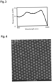
- Fig. 3 shows a diagram depicting the responsivity of an embodiment of the imaging sensor 20 according to the invention as a function of wavelength. As can be seen, the imaging sensor 20 achieves a responsivity of 1.0 or more over most of the spectrum in the range of from 800 to 3300 nm.
- step a a plurality of pre-determined wavelengths within a target wavelength range is chosen (see step S1 in Fig. 7 ).
- the target wavelength range is determined based on the intended application of the imaging sensor 20.
- the imaging sensor 20 is an NIR imaging sensor which is supposed to detect light having a wavelength in a target range of from 500 to 3000 nm.
- the pre-determined wavelengths need to be chosen within said target range, preferably equally spaced within the target range.
- a quantum dot precursor having an average diameter corresponding to one of the pre-determined wavelengths is provided (see step S2 in Fig. 7 ).
- Preparation methods for quantum dot precursors are known in the art. One example for preparing a quantum dot precursor will be described later.
- step c an ink formulation comprising the quantum dot precursor and a solvent is prepared (see step S3 in Fig. 7 ).
- the solvent is especially chosen from the group consisting of N,N-dimethylformamide (DMF), hexylamine (HEX), butylamine (BTA), phenylethylamine (PEA), dimethylsulfoxide (DMSP) and combinations thereof.
- DMF N,N-dimethylformamide
- HEX hexylamine
- BTA butylamine
- PEA phenylethylamine
- DMSP dimethylsulfoxide
- step d) the ink formulation is applied on the substrate 26, i.e. on the finger-structure electrodes 24 of one of the detector elements 22 in the shown embodiment, thereby forming one of the plurality of detector elements 22 (see step S4 in Fig. 7 ).
- Steps b) to d) are then repeated for each of the pre-determined wavelengths to form all of the detector elements 22, such that the average diameter of the quantum dots increase along the array axis L of the array structure.
- steps b) to d) can also be done in an interleaved manner.
- at least some of the ink formulations can already be prepared when one of the ink formulation is currently already applied on the substrate.
- a 250 mL three-neck flask is filled with 900 mg (4 mmol) PbO and 30.35 mL (95 mmol) 1-octadecene inside of a nitrogen filled glovebox. Afterwards, the flask is mounted onto a Schlenk line, evacuated and flushed with nitrogen for three times. Under nitrogen flow, 37.8 g (144 mmol) oleic acid is added. The solution is heated to 150°C under vacuum for one hour. During this time, the solution is degassed and the yellow color disappeared, meaning that the lead oleate precursor is formed.
- the sulfur precursor solution consisting of 420 ⁇ L (2 mmol) bis-(trimethylsilyl)-sulfide (TMS-S) in 5.0 mL (15.6 mmol) 1-octadecene, is injected into the lead oleate precursor solution and the reaction was stirred for exactly 5 minutes, then quenched in an ice bath for at least 2.5 minutes.
- the solution is loaded into four centrifuge tubes.
- the quantum dots (QDs) in each tube are precipitated with 10 mL ethanol and 10 mL acetone, followed by centrifugation (7860 rpm, 10 minutes) and discarding the supernatant.
- the washing process was repeated twice by redispersing the sediment in 15 mL octane using the vortex and precipitating the PbS quantum dots with 10 mL ethanol and 10 mL acetone, followed by centrifugation (7860 rpm, 10 minutes) and removing the supernatant.
- the PbS quantum dots in the sediment are dried in vacuum and redispersed in toluene at a concentration of 40 mg/mL for long-term storage.
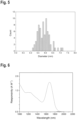
- Fig. 4 shows a TEM image of oleate-capped PbS quantum dots with an absorption edge of 1710 nm
- Fig. 5 a histogram of a representative region from the TEM image comprising a total of 75 quantum dots with an average diameter of 5.91 ⁇ 0.41 nm.
- PbS quantum dots can be synthesized such to obtain a precise size control of the synthesized quantum dots.
- the synthesized oleate-capped PbS quantum dots in toluene are precipitated with acetone, dried and dissolved in octane at a concentration of 60 mg/mL. Furthermore, 922 mg (2 mmol) PbI 2 , 146.8 mg (0.5 mmol) PbBr 2 and 72.2 mg (0.88 mmol) sodium acetate are dissolved in 20 mL DMF as ligand precursor solution.
- Two centrifuge tubes are loaded with 30 mL octane, 1 mL of the oleate-capped PbS in octane and 10 mL of the ligand precursor solution each.
- the tube is shaken for 30 s by hand, centrifuged (7860 rpm, 30 sec) and the octane phase is removed.
- the octane phase became clear and the quantum dots moved into the polar DMF phase.
- the DMF phase is washed three times. Each step consisted of the addition of 10 mL octane, shaking for 30 seconds, centrifugation and final removal of the octane phase. In the last step, all solvents, i.e. the octane and DMF phase, are removed.
- the quantum dots are partially redispersed in 250 ⁇ L DMF by vortexing. For full dissolution, 10 ⁇ L of BTA is added. The solution of both tubes is moved into a single 2 mL centrifuge tube, in which the quantum dots are precipitated with 800 ⁇ L toluene and centrifuged at 13.000 rpm for 3 minutes.
- the PbS quantum dots are dissolved in 500 ⁇ L DMF and 10 ⁇ L BTA, precipitated with 1 mL toluene and centrifuged at 13.000 rpm for 5 minutes.
- the pellet obtained from synthesis of core-shell quantum dots is moved into a glass vial and an ink is prepared by adding a suitable solvent.
- Possible solvent mixtures include DMF:DMSP:BTA:PEA and HEX:DMF:BTA.
- An ink consisting of DMF:HEX:BTA in the ratio of 1:1:1 (v/v) has an approximate boiling point of 120°C which ensures a fast film solidification.
- the concentration for the thin film fabrication is 450 mg/mL.
- the ink can be directly applied onto the substrate and the solvent be evaporated to form the quantum dots on the substrate.
- the ink can be centrifuged exactly 30 s and the supernatant is used for the application of the ink, e.g. by blade coating.
- Photoconductivity experiments were done with a tungsten lamp used as illumination source which was mono-achromatized by a grating spectrometer ("Acton SP 2150" from “Princeton” company).
- the output tuned light obtained from the grating spectrometer was modulated with a mechanical chopper.
- the detector On the sample side, the detector was biased with a "Keithley 236 SMU” source measure unit.
- the output current was read through a "Signal Recovery 7265 DSP" lock-in amplifier.
- Fig. 6 shows an exemplary responsivity graph as a function of wavelength for a detector element having quantum dots with an absorption maximum at 1650 nm.
Landscapes
- Photometry And Measurement Of Optical Pulse Characteristics (AREA)
- Solid State Image Pick-Up Elements (AREA)
Abstract
Description
- The invention relates to an imaging sensor comprising light-sensitive detector elements with quantum dots, a sensor system comprising such an imaging sensor and a method for manufacturing an imaging sensor.
- In spectroscopy applications, a sample is irradiated with light, i.e. electromagnetic radiation of a given range of wavelengths defining a light spectrum. By interaction of the sample with the light, e.g. by absorption, the light spectrum is characteristically changed, such that information about the sample can be derived from the changed light spectrum.
- A core component of any given spectroscopy setup is the imaging sensor which is used to detect the light after interaction with the sample. Typically, imaging sensors comprise a multitude of small light-sensitive areas (also termed "pixels") spread along one or two axes of the imaging sensor. The signals obtained from each individual pixel is then used to assemble an overall image of the area of interest.
- E.g., in NIR (near-infrared) applications, InGaAs-based multi-channel array detectors are used for detecting infrared light due to their high sensitivity to light in the NIR spectrum.
- In a typical spectrometer, the light for detection is spread as a function of its wavelength by an optical element like a grating along at least one of the axes of the imaging sensor. Thus, the pixel at one end of the respective axis will be irradiated with light of a minimum wavelength, the neighboring pixel with light of a slightly higher wavelength, the next-neighboring pixel with light of an even slightly higher wavelength and so on until the pixel at the other end of the respective axis will be irradiated with light of a maximum wavelength.
- Known imaging sensors suffer from limitations based on their performance and their spectral response, which can be expressed in terms of their responsivity. The responsivity measures an input-output gain of a given imaging sensor and is a ratio between the electrical output power and the optical input power. Here, the responsivity is expressed in terms of current responsivity Ri which can be expressed by the following equation (1):

- In commercially available imaging sensors based on InGaAs, the spectral response or responsivity is less than 1 A/W over considerable parts of the VIS and NIR spectrum. This directly influences the specific detectivity of the imaging sensor, which describes the smallest optical input which can be sensed by the detector, wherein the smallest optical input power (also called "noise equivalent power" PNEP) can be described as PNEP = Inoise/Ri, wherein Inoise defines electrical noise which is a random variable resulting from stochastic or random processes associated with various particles.
- In the last years, alternatives to InGaAs-based detector elements have been investigated, e.g. Bulk PbS NIR-sensitive materials, PbS quantum dots, combinations of graphene and PbS quantum dots and NIR sensitive polymers. However, none of these alternatives reach the same performance as InGaAs-based detector elements.
- The object of the invention is to provide an imaging sensor with high responsivity, especially with a uniform responsivity over extended parts of the light spectrum.
- The object of the invention is solved by an imaging sensor comprising a plurality of light-sensitive detector elements being arranged in an array structure, the detector elements comprising quantum dots, wherein the average diameter of the quantum dots of the detector elements increase along an array axis of the array structure such that each of the detector elements along the array axis has an absorption maximum at a different pre-determined wavelength.
- The invention is based on the idea to use a multitude of different sized quantum dots along the array structure of the imaging sensor such that at every point along the array axis quantum dots are used which are optimal for the light of the specific wavelength irradiated on the respective point of the imaging sensor along the array axis. Termed differently, the imaging sensor according to the invention uses selective quantum dots with a tuned size at selected positions along the array axis for increasing the quantum efficiency at each individual wavelength detectable by the imaging sensor, thereby optimizing the overall responsivity of the imaging sensor. This effect is based on the effect that quantum dots show an absorption maximum at a wavelength which is dependent on the size of the quantum dots.
- In contrast, in conventional InGaAs-based imaging sensors, the same type of InGaAs-based detector element is used at all pixels of the imaging sensor. Thus, wavelengths at which the respective kind of detector element has a low responsivity cannot be compensated for, leading to an overall suboptimal responsivity of the conventional imaging sensor.
- The detector elements are also termed "pixels", wherein the totality of pixels define the picture obtained by the imaging sensor.
- The average diameter of the quantum dots can be determined by taking a TEM-image of the respective detector element, measuring the individual quantum dot diameter throughout the detector element and calculating the average value of the measured individual quantum dot diameters.
- Generally, the term "quantum dot" defines a crystalline material having a size of several nanometers and which is composed of hundreds to thousands of atoms. Due to the small size of these materials, most of the atoms are present on or near the surface of the quantum dots which leads to electronic, optical, chemical and mechanical properties different from those of a bulk crystalline material due to quantum confinement effects.
- Each detector element can comprise at least two sub-elements, wherein all sub-elements of a detector element comprise quantum dots of the same average diameter. The use of several sub-elements can at least partially compensate for effects of limited resolution of light falling onto the imaging sensor.
- The term "same average diameter" means that the quantum dots within all sub-elements of the detector element have the same average diameter wherein unavoidable variations due to the manufacturing process of the imaging sensor are ignored.
- The quantum dots can comprise a semiconductive material, the semiconductive material preferably being selected from the group consisting of PbS, PbSe, HgTe, InAs, InSb, CdS, CdSe and combinations thereof, more preferably wherein the semiconductive material of the quantum dots is PbS. Quantum dots of these materials show an absorption maximum at wavelengths typically needed in spectroscopy applications, especially for VIS- and/or NIR-applications. Further, quantum dots of selected sizes can be efficiently prepared from these materials by synthesis routes known in the art.
- To improve the conductivity of the quantum dots in the detector element, the quantum dots can have a core-shell structure. Further, using quantum dots with a core-shell structure can improve the robustness and/or lifetime of the imaging sensor.
- The core preferably comprises the semiconductive material.
- The shell preferably comprises ligands bonded to the core. The ligand can be chosen from the group of carboxylic acids, thioles, amines, organic salts and combinations thereof.
- The carboxylic acid is preferably selected from the group of saturated or unsaturated fatty acids having a chain length of from 2 to 22 carbon atoms. E.g., the carboxylic acid can be selected from the group consisting of lauric acid, myristic acid, stearic acid, oleic acid and combinations thereof. Most preferably, the carboxylic acid is oleic acid.
- The thiol is preferably selected from the group of saturated or unsaturated thiols having a chain length of from 2 to 8 carbon atoms. Most preferably, the thiol is ethanedithiol, 3-mercaptopropionic acid or a combination thereof.
- The amine is preferably selected from the group of saturated and unsaturated amines having a chain length of from 2 to 20 carbon atoms. Most preferably, the amine is butylamine, oleylamine or a combination thereof.
- The organic salt preferably is selected from the group of quaternary ammonium salts. Most preferably, the organic salt is a tetrabutylammonium salt, a cetyltrimethyl ammonium salt or a combination thereof, e.g. cetyltrimethyl ammonium bromide.
- The average diameter of the quantum dots can be within the range of from 3 to 20 nm. Quantum dots of this size range show absorption maxima in the VIS- to NIR-range of the light spectrum, thereby rendering these materials especially suitable for VIS- and/or NIR-spectroscopy applications.
- Generally, the shape of the quantum dots is not restricted, as long as they show the desired absorption behavior.
- In one variant, the quantum dots have a circular or a polygonal shape. The polygonal shape is e.g. a five- or six-sided polygonal shape. The polygonal shape is defined as the contour of the outer edge of the respective quantum dot in a two-dimensional TEM-image.
- The imaging sensor especially is an NIR imaging sensor, preferably wherein the imaging sensor is adapted to detect light having a wavelength in a target range of from 500 to 3000 nm, more preferably of from 800 to 2500 nm.
- The "target range" defines the target spectrum of the imaging sensor.
- The imaging sensor can have a responsivity of 1 or more over at least 85% of the target range, preferably over at least 90 % of the target range. In this way, the imaging sensor provides an especially high overall sensitivity.
- The object of the invention is further solved by a sensor system comprising the imaging sensor as described above being adapted to detect light from an incident light beam and at least one optical element configured to guide the incident light beam onto the imaging sensor.
- The properties and advantages of the imaging sensor according to the invention also apply to the sensor system according to the invention and vice versa and it is referred to the explanations given above.
- The at least one optical element especially comprises an optical slit or optical filter and a grating. The optical slit or optical filter limits the size and/or intensity of an incoming light beam. The grating is used for generating a dispersed incident light beam which is detected by the imaging sensor.
- The pre-determined wavelengths of the quantum dots used in the imaging sensor is especially defined by the resolution of the grating. Termed differently, the grating can determine the available dispersion resolution and the quantum dots in the respective detector elements are chosen such to optimally correspond to the available wavelength resolution. Generally, the resolution of the sensor system is determined by the resolution of the grating, as commercially available gratings typically have a resolution of 5 to 10 nm.
- The object of the invention is also solved by a method for manufacturing an imaging sensor comprising a plurality of light-sensitive detector elements being arranged in an array structure, the detector elements comprising quantum dots, the method comprising the steps of:
- a) choosing a plurality of pre-determined wavelengths within a target wavelength range,
- b) providing a quantum dot precursor having an average diameter corresponding to one of the pre-determined wavelengths,
- c) preparing an ink formulation comprising the quantum dot precursor and a solvent, and
- d) applying the ink formulation on a substrate, thereby forming one of the plurality of detector elements comprising quantum dots,
- The imaging sensor especially is an imaging sensor as described above.
- The method according to the invention provides an easy and reliable way of applying quantum dots of selected sizes having absorption maxima at the pre-determined wavelengths onto the substrate, thereby obtaining an imaging sensor of optimal responsivity and sensitivity. Termed differently, the method according to the invention is based on a combination of using selectively sized quantum dots with a method of additive manufacturing, e.g. inkjet printing of ink formulations comprising quantum dots.
- Generally, the method for applying the ink formulation on the substrate is not limited, as long as the respective ink formulation can be reliably applied on the substrate. E.g., the ink formulation can be applied by blade coating, slot die coating, spray coating and/or inkjet printing.
- The quantum dot precursor can comprise colloidal quantum dots within a solvent. The colloidal quantum dots can be capped by a ligand such to form a core-shell structure. Quantum dot precursors can be prepared in advance and stored for extended period of times, especially if core-shell structured quantum dots are used. Thus, the necessary quantum dot precursors can be flexibly chosen before the respective manufacturing process at hand.
- The solvent can be chosen from the group consisting of N,N-dimethylformamide, hexylamine, butylamine, phenylethylamine, dimethylsulfoxide and combinations thereof.
- The solvent used in the ink formulation preferably has a boiling point of 130 °C or less. Solvents or solvent mixtures with a boiling point of 130 °C or less provide a fast solidification of the ink formulation on the substrate after application, thereby reducing the amount of material movement between application of the ink and ink solidification and thus increasing the homogeneity of the formed detector element.
- For increasing the density of quantum dots within the detector elements, the quantum dot precursor can have a concentration of at least 300 mg/mL in the ink formulation, preferably of at least 400 mg/mL.
- The substrate can be a finger-structure electrode. Such electrodes lead to an especially easy and fast manufacturing method, as no additional steps other than applying the ink formulation on the finger-structure electrode and drying the ink formulation has to be applied to obtain a functional imaging sensor.
- E.g., the detector element can be a photoresistor device.
- It is also possible that the substrate comprises a metal oxide layer on which the ink formulation is applied. Thus, the quantum dots will be on top of the metal oxides, forming a multiple layer structure with the substrate.
- The kind of substrate is generally not limited, as long as the ink formulation can be homogenously applied on the respective substrate.
- Further features and advantages of the invention will become more apparent from the following detailed description of exemplary embodiments, which are not be understood as limiting, the experiments and Figures.
-
Fig. 1 schematically shows a sensor system according to the invention comprising an imaging sensor according to the invention, -
Fig. 2 schematically shows the imaging sensor ofFig. 1 in more detail. -
Fig. 3 shows a diagram depicting the responsivity of the imaging sensor ofFig. 1 as a function of wavelength, -
Fig. 4 shows a TEM image of quantum dots used in the imaging sensor ofFig. 1 applied on a substrate, -
Fig. 5 shows a diagram highlighting the size distribution of the quantum dots inFig. 4 , -
Fig. 6 shows an absorption spectrum of one type of quantum dots used in the imaging sensor ofFig. 1 , and -
Fig. 7 shows a block diagram of a method according to the invention for manufacturing the imaging sensor ofFig. 1 . - In
Fig. 1 , a schematic depiction of selected parts of asensor system 10 according to the invention is shown. - The
sensor system 10 comprises severaloptical elements 12, wherein in the embodiment shown inFig. 1 thesensor system 10 comprises anoptical slit 14 and a grating 16 asoptical elements 12. - The
optical slit 14 is used to limit the size and of anincoming light beam 18 before saidincident light beam 18 falls upon thegrating 16. The grating 16 disperses theincident light beam 18. The dispersedincident light beam 18 is then directed onto animaging sensor 20 according to the invention. - Of course, the kind of
optical elements 12, the number ofoptical elements 12 and their relative arrangement can differ from the exemplary embodiment shown inFig. 1 . - The
imaging sensor 20 comprises a plurality of light-sensitive detector elements 22 which are arranged in an array structure along an array axis L of theimaging sensor 20. - Each of the
detector elements 22 comprises quantum dots (seeFig. 4 ), wherein the size of the quantum dots generally increase along the array axis L. E.g., the average diameter of the quantum dots is within a range of from 3 to 20 nm. - The quantum dots comprise a semiconductive material, the semiconductive material being selected from the group consisting of PbS, PbSe, HgTe, InAs, InSb, CdS, CdSe and combinations thereof.
- Due to the different sizes of the quantum dots, the absorption maximum of the respective quantum dots, i.e. the wavelength for which the respective quantum shows the highest responsivity, also changes along the array axis L of the
imaging sensor 20. - According to the invention, the average diameter of the quantum dots along the array axis L (and therefore the absorption maxima of the quantum dots) is chosen such that the position of each of the
detection elements 22 along the array axis L is matched with the wavelength of theincident light beam 18 after it has been dispersed by thegrating 16. Termed differently, each of thedetector elements 22 has an absorption maximum at or close to the wavelength of the light which is directed by the grating 16 on therespective detector element 22. -
Fig. 2 shows a further schematic depiction of theimaging sensor 20 with more details. - Each of the
detector elements 22 comprises a plurality ofsub-elements 24, in the shown embodiment a total of foursub-elements 24, as indicated inFig. 2 by rectangles having differing contours. Of course, each of thedetector elements 22 can also comprise a lower or higher number ofdetector elements 22. - Each of the sub-elements 24 is a finger-structure electrode which acts as a
substrate 26 for the quantum dots. The finger-structure electrodes are connected via connection terminals 28 to (not shown) read-out electronics of theimaging sensor 20. Accordingly, a charge built up in the quantum dots on the substrate upon irradiation can be quantified and evaluated. - Within each of the
detector elements 22, quantum dots of the same average diameter are applied on the finger-structure electrodes, wherein the average diameter is increasing along the array axis L, such that each of thedetector elements 22 has an absorption maximum at a pre-determined wavelength. - E.g., the
detector element 22 depicted at the left-hand side ofFig. 2 is thedetector element 22 with the smallest quantum dots and therefore with an absorption maximum at the lowest wavelength compared to all other quantum dots used in the imaging sensor. Thedetector element 22 depicted at the right-hand side ofFig. 2 is thedetector element 22 with the largest quantum dots and therefore with an absorption maximum at the highest wavelength compared to all other quantum dots used in the imaging sensor. - In
Fig. 2 , animaging sensor 20 having a total of eightdetector elements 22, each having foursub-elements 24, is shown. Of course, the number ofdetector elements 22 can be lower or higher than shown inFig. 2 . E.g., theimaging sensor 20 can comprise up to several thousand ofdetector elements 22. - Preferably, the number of
detector elements 22 is matched to the resolution of the grating 16, i.e. the number ofdetector elements 22, the number ofsub-elements 24 within eachdetector element 22 and/or the spacing between twodetector elements 22 is chosen to correspond to the resolution of grating 16. -
Fig. 3 shows a diagram depicting the responsivity of an embodiment of theimaging sensor 20 according to the invention as a function of wavelength. As can be seen, theimaging sensor 20 achieves a responsivity of 1.0 or more over most of the spectrum in the range of from 800 to 3300 nm. - For this measurement, a linear array imaging sensor with quantum dots of 18 different average diameters, i.e. having 18 different absorption maxima, has been used, wherein the overall detection range of the imaging sensor was from 400 to 3300 nm.
- For determining the power input Pin of the used light source as function of wavelength, a calibration measurement was done over the relevant spectrum using a combination of conventional imaging sensors based on silicon, InGaAs and pyroelectric thermodetectors, respectively, to cover the whole target spectrum from visible to the mid-infrared regime. Then, the current output ΔI using the linear imaging sensor with quantum dots was measured as a function of wavelength and the responsivity was calculated according to formula (1) as described above.
- In the following, a method for manufacturing the image sensor as described above is presented.
- First, as step a), a plurality of pre-determined wavelengths within a target wavelength range is chosen (see step S1 in
Fig. 7 ). The target wavelength range is determined based on the intended application of theimaging sensor 20. - E.g., the
imaging sensor 20 is an NIR imaging sensor which is supposed to detect light having a wavelength in a target range of from 500 to 3000 nm. Thus, the pre-determined wavelengths need to be chosen within said target range, preferably equally spaced within the target range. - Second, as step b), a quantum dot precursor having an average diameter corresponding to one of the pre-determined wavelengths is provided (see step S2 in
Fig. 7 ). Preparation methods for quantum dot precursors are known in the art. One example for preparing a quantum dot precursor will be described later. - As step c), an ink formulation comprising the quantum dot precursor and a solvent is prepared (see step S3 in
Fig. 7 ). - The solvent is especially chosen from the group consisting of N,N-dimethylformamide (DMF), hexylamine (HEX), butylamine (BTA), phenylethylamine (PEA), dimethylsulfoxide (DMSP) and combinations thereof.
- Finally, as step d), the ink formulation is applied on the
substrate 26, i.e. on the finger-structure electrodes 24 of one of thedetector elements 22 in the shown embodiment, thereby forming one of the plurality of detector elements 22 (see step S4 inFig. 7 ). - Steps b) to d) are then repeated for each of the pre-determined wavelengths to form all of the
detector elements 22, such that the average diameter of the quantum dots increase along the array axis L of the array structure. - Of course, the iteration of steps b) to d) can also be done in an interleaved manner. E.g., at least some of the ink formulations can already be prepared when one of the ink formulation is currently already applied on the substrate.
- For the synthesis of PbS quantum dots with an absorption edge at about 1700 nm, a 250 mL three-neck flask is filled with 900 mg (4 mmol) PbO and 30.35 mL (95 mmol) 1-octadecene inside of a nitrogen filled glovebox. Afterwards, the flask is mounted onto a Schlenk line, evacuated and flushed with nitrogen for three times. Under nitrogen flow, 37.8 g (144 mmol) oleic acid is added. The solution is heated to 150°C under vacuum for one hour. During this time, the solution is degassed and the yellow color disappeared, meaning that the lead oleate precursor is formed.
- Afterwards, the solution is cooled to 120°C under a nitrogen atmosphere. The sulfur precursor solution, consisting of 420 µL (2 mmol) bis-(trimethylsilyl)-sulfide (TMS-S) in 5.0 mL (15.6 mmol) 1-octadecene, is injected into the lead oleate precursor solution and the reaction was stirred for exactly 5 minutes, then quenched in an ice bath for at least 2.5 minutes.
- For purification, the solution is loaded into four centrifuge tubes. The quantum dots (QDs) in each tube are precipitated with 10 mL ethanol and 10 mL acetone, followed by centrifugation (7860 rpm, 10 minutes) and discarding the supernatant. The washing process was repeated twice by redispersing the sediment in 15 mL octane using the vortex and precipitating the PbS quantum dots with 10 mL ethanol and 10 mL acetone, followed by centrifugation (7860 rpm, 10 minutes) and removing the supernatant.
- The PbS quantum dots in the sediment are dried in vacuum and redispersed in toluene at a concentration of 40 mg/mL for long-term storage.
- For the synthesis of PbS quantum dots with an absorption edge at about 950 nm for the HTL, minor changes during the synthesis method described above are employed.
- 900 mg PbO are dissolved in 52.5 mL 1-octadecene and 3.2 mL oleic acid is used as the ligand. The sulfur precursor solution was not changed, i.e. 420 µL TSM-S in 5 mL 1-octadecene. During the injection, the temperature was lowered to 100°C. All other steps are kept the same as described above.
- From the above, it is clear that the same procedure can be followed for obtaining PbS quantum dots of a target size having an absorption maximum at a pre-determined wavelength.
-
Fig. 4 shows a TEM image of oleate-capped PbS quantum dots with an absorption edge of 1710 nm andFig. 5 a histogram of a representative region from the TEM image comprising a total of 75 quantum dots with an average diameter of 5.91 ± 0.41 nm. - From these Figures, it becomes evident that PbS quantum dots can be synthesized such to obtain a precise size control of the synthesized quantum dots.
- The synthesized oleate-capped PbS quantum dots in toluene are precipitated with acetone, dried and dissolved in octane at a concentration of 60 mg/mL. Furthermore, 922 mg (2 mmol) PbI2, 146.8 mg (0.5 mmol) PbBr2 and 72.2 mg (0.88 mmol) sodium acetate are dissolved in 20 mL DMF as ligand precursor solution.
- Two centrifuge tubes are loaded with 30 mL octane, 1 mL of the oleate-capped PbS in octane and 10 mL of the ligand precursor solution each. The tube is shaken for 30 s by hand, centrifuged (7860 rpm, 30 sec) and the octane phase is removed.
- During this step, the octane phase became clear and the quantum dots moved into the polar DMF phase. To remove all organic ligand impurities, the DMF phase is washed three times. Each step consisted of the addition of 10 mL octane, shaking for 30 seconds, centrifugation and final removal of the octane phase. In the last step, all solvents, i.e. the octane and DMF phase, are removed.
- The quantum dots are partially redispersed in 250 µL DMF by vortexing. For full dissolution, 10 µL of BTA is added. The solution of both tubes is moved into a single 2 mL centrifuge tube, in which the quantum dots are precipitated with 800 µL toluene and centrifuged at 13.000 rpm for 3 minutes.
- Afterwards, the PbS quantum dots are dissolved in 500 µL DMF and 10 µL BTA, precipitated with 1 mL toluene and centrifuged at 13.000 rpm for 5 minutes.
- The pellet obtained from synthesis of core-shell quantum dots is moved into a glass vial and an ink is prepared by adding a suitable solvent.
- Possible solvent mixtures include DMF:DMSP:BTA:PEA and HEX:DMF:BTA.
- An ink consisting of DMF:HEX:BTA in the ratio of 1:1:1 (v/v) has an approximate boiling point of 120°C which ensures a fast film solidification.
- The concentration for the thin film fabrication is 450 mg/mL.
- The ink can be directly applied onto the substrate and the solvent be evaporated to form the quantum dots on the substrate.
- To remove further remaining particles, the ink can be centrifuged exactly 30 s and the supernatant is used for the application of the ink, e.g. by blade coating.
- Photoconductivity experiments were done with a tungsten lamp used as illumination source which was mono-achromatized by a grating spectrometer ("Acton SP 2150" from "Princeton" company). The output tuned light obtained from the grating spectrometer was modulated with a mechanical chopper. On the sample side, the detector was biased with a "Keithley 236 SMU" source measure unit. The output current was read through a "Signal Recovery 7265 DSP" lock-in amplifier.
-
Fig. 6 shows an exemplary responsivity graph as a function of wavelength for a detector element having quantum dots with an absorption maximum at 1650 nm.
Claims (15)
- An imaging sensor comprising a plurality of light-sensitive detector elements being arranged in an array structure, the detector elements comprising quantum dots,
wherein the average diameter of the quantum dots of the detector elements increase along an array axis of the array structure such that each of the detector elements along the array axis has an absorption maximum at a different pre-determined wavelength. - The imaging sensor according to claim 1, wherein each detector element comprises at least two sub-elements, wherein all sub-elements of a detector element comprise quantum dots of the same average diameter.
- The imaging sensor according to claim 1 or 2, wherein the quantum dots comprise a semiconductive material, the semiconductive material preferably being selected from the group consisting of PbS, PbSe, HgTe, InAs, InSb, CdS, CdSe and combinations thereof, more preferably wherein the semiconductive material of the quantum dots is PbS.
- The imaging sensor according to any of the preceding claims, wherein the quantum dots have a core-shell structure.
- The imaging sensor according to any of the preceding claims, wherein the average diameter of the quantum dots is within the range of from 3 to 20 nm.
- The imaging sensor according to any of the preceding claims, wherein the quantum dots have a circular or polygonal shape.
- The imaging sensor according to any of the preceding claims, wherein the imaging sensor is an NIR imaging sensor, especially wherein the imaging sensor is adapted to detect light having a wavelength in a target range of from 500 to 3000 nm, preferably of from 800 to 2500 nm.
- The imaging sensor according to claim 7, wherein the imaging sensor has a responsivity of 1 or more over at least 85% of the target range, preferably over at least 90 % of the target range.
- A sensor system comprising the imaging sensor according to any of the preceding claims being adapted to detect light from an incident light beam and at least one optical element configured to guide the incident light beam onto the imaging sensor.
- A method for manufacturing an imaging sensor comprising a plurality of light-sensitive detector elements being arranged in an array structure, the detector elements comprising quantum dots, the method comprising the steps of:a) choosing a plurality of pre-determined wavelengths within a target wavelength range,b) providing a quantum dot precursor having an average diameter corresponding to one of the pre-determined wavelengths,c) preparing an ink formulation comprising the quantum dot precursor and a solvent, andd) applying the ink formulation on a substrate, thereby forming one of the plurality of detector elements comprising quantum dots,wherein steps b) to d) are repeated for each of the pre-determined wavelengths and wherein the ink formulations are applied on the substrate such that the average diameter of the quantum dots in the formed detector elements increases along an array axis of the array structure.
- The method of claim 10, wherein the solvent is chosen from the group consisting of N,N-dimethylformamide, hexylamine, butylamine, phenylethylamine, dimethylsulfoxide and combinations thereof.
- The method of claim 10 or 11, wherein the solvent used in the ink formulation has a boiling point of 130 °C or less.
- The method of any of claims 10 to 12, wherein the quantum dot precursor has a concentration of at least 300 mg/mL in the ink formulation, preferably of at least 400 mg/mL.
- The method of any of claims 10 to 13, wherein the substrate is a finger-structure electrode.
- The method of any of claims 10 to 14, wherein the substrate comprises a metal oxide layer on which the ink formulation is applied.
Priority Applications (4)
| Application Number | Priority Date | Filing Date | Title |
|---|---|---|---|
| EP23152976.9A EP4407685B1 (en) | 2023-01-24 | 2023-01-24 | Imaging sensor comprising quantum dots, sensor system and method for manufacturing an imaging sensor |
| US19/150,303 US20260231540A1 (en) | 2023-01-24 | 2024-01-16 | Imaging sensor comprising quantum dots, sensor system and method for manufacturing an imaging sensor |
| PCT/EP2024/050896 WO2024156541A1 (en) | 2023-01-24 | 2024-01-16 | Imaging sensor comprising quantum dots, sensor system and method for manufacturing an imaging sensor |
| EP24700323.9A EP4655823A1 (en) | 2023-01-24 | 2024-01-16 | Imaging sensor comprising quantum dots, sensor system and method for manufacturing an imaging sensor |
Applications Claiming Priority (1)
| Application Number | Priority Date | Filing Date | Title |
|---|---|---|---|
| EP23152976.9A EP4407685B1 (en) | 2023-01-24 | 2023-01-24 | Imaging sensor comprising quantum dots, sensor system and method for manufacturing an imaging sensor |
Publications (2)
| Publication Number | Publication Date |
|---|---|
| EP4407685A1 true EP4407685A1 (en) | 2024-07-31 |
| EP4407685B1 EP4407685B1 (en) | 2025-11-12 |
Family
ID=85076368
Family Applications (2)
| Application Number | Title | Priority Date | Filing Date |
|---|---|---|---|
| EP23152976.9A Active EP4407685B1 (en) | 2023-01-24 | 2023-01-24 | Imaging sensor comprising quantum dots, sensor system and method for manufacturing an imaging sensor |
| EP24700323.9A Pending EP4655823A1 (en) | 2023-01-24 | 2024-01-16 | Imaging sensor comprising quantum dots, sensor system and method for manufacturing an imaging sensor |
Family Applications After (1)
| Application Number | Title | Priority Date | Filing Date |
|---|---|---|---|
| EP24700323.9A Pending EP4655823A1 (en) | 2023-01-24 | 2024-01-16 | Imaging sensor comprising quantum dots, sensor system and method for manufacturing an imaging sensor |
Country Status (3)
| Country | Link |
|---|---|
| US (1) | US20260231540A1 (en) |
| EP (2) | EP4407685B1 (en) |
| WO (1) | WO2024156541A1 (en) |
Families Citing this family (1)
| Publication number | Priority date | Publication date | Assignee | Title |
|---|---|---|---|---|
| CN119153479B (en) * | 2024-09-18 | 2025-03-28 | 甘肃省科学院传感技术研究所 | A high-sensitivity wide-spectrum true-color quantum dot image sensor and its preparation method |
Citations (4)
| Publication number | Priority date | Publication date | Assignee | Title |
|---|---|---|---|---|
| US20050205879A1 (en) * | 2004-03-17 | 2005-09-22 | Fuji Photo Film Co., Ltd. | Photoelectric converting film stack type solid-state image pickup device |
| US20080315339A1 (en) * | 2006-10-23 | 2008-12-25 | John Rennie | Solid-state imaging device |
| US20180342647A1 (en) * | 2011-11-22 | 2018-11-29 | Samsung Electronics Co., Ltd. | Coated semiconductor nanocrystals and products including same |
| EP3979333A1 (en) * | 2019-05-31 | 2022-04-06 | FUJIFILM Corporation | Optical sensor and sensing device |
-
2023
- 2023-01-24 EP EP23152976.9A patent/EP4407685B1/en active Active
-
2024
- 2024-01-16 EP EP24700323.9A patent/EP4655823A1/en active Pending
- 2024-01-16 US US19/150,303 patent/US20260231540A1/en active Pending
- 2024-01-16 WO PCT/EP2024/050896 patent/WO2024156541A1/en not_active Ceased
Patent Citations (4)
| Publication number | Priority date | Publication date | Assignee | Title |
|---|---|---|---|---|
| US20050205879A1 (en) * | 2004-03-17 | 2005-09-22 | Fuji Photo Film Co., Ltd. | Photoelectric converting film stack type solid-state image pickup device |
| US20080315339A1 (en) * | 2006-10-23 | 2008-12-25 | John Rennie | Solid-state imaging device |
| US20180342647A1 (en) * | 2011-11-22 | 2018-11-29 | Samsung Electronics Co., Ltd. | Coated semiconductor nanocrystals and products including same |
| EP3979333A1 (en) * | 2019-05-31 | 2022-04-06 | FUJIFILM Corporation | Optical sensor and sensing device |
Also Published As
| Publication number | Publication date |
|---|---|
| EP4655823A1 (en) | 2025-12-03 |
| US20260231540A1 (en) | 2026-08-06 |
| EP4407685B1 (en) | 2025-11-12 |
| WO2024156541A1 (en) | 2024-08-02 |
Similar Documents
| Publication | Publication Date | Title |
|---|---|---|
| Hafiz et al. | Colloidal quantum dots for thermal infrared sensing and imaging | |
| US8440997B2 (en) | Nanowire photodetector and image sensor with internal gain | |
| US12015093B2 (en) | Multi-band infrared imaging using stacked colloidal quantum-dot photodiodes | |
| Williamson et al. | Near-infrared Raman spectroscopy with a 783-nm diode laser and CCD array detector | |
| US6967345B1 (en) | Dual band QWIP focal plane array | |
| EP4407685B1 (en) | Imaging sensor comprising quantum dots, sensor system and method for manufacturing an imaging sensor | |
| Al Mahfuz et al. | Colloidal Ag2Se intraband quantum dots | |
| US10866143B2 (en) | Infrared photodetection system | |
| Buurma et al. | Advances in HgTe colloidal quantum dots for infrared detectors | |
| Gunapala et al. | 640× 512 pixel narrow-band, four-band, and broad-band quantum well infrared photodetector focal plane arrays | |
| Cabalin et al. | Fast spatially resolved surface-enhanced Raman spectrometry on a silver coated filter paper using charge-coupled device detection | |
| Di et al. | Dual-Band Infrared PbS Colloidal Quantum Dot Focal Plane Array | |
| WO2021028175A1 (en) | Method and device for analysing a multiple solar cell with at least two sub-solar cells by means of luminescent radiation | |
| US7282691B2 (en) | Method for determining wavelengths of light incident on a photodetector | |
| US20220155152A1 (en) | Infrared photodetection device, infrared photodetection process, computer program, and computer-readable storage medium containing program | |
| KR101549193B1 (en) | Apparatus for detecting atmosphere condition photon having function of adjusting intensity of light and the adjusting method thereof | |
| Péré-Laperne et al. | Extended shortwave infrared technological developments at Lynred | |
| US4531059A (en) | Non-delineated semiconductor detector array for infra-red | |
| DE19727693A1 (en) | Method and device for producing electrically conductive passages in semiconductor components | |
| US9634173B2 (en) | Photodetector for determining light wavelengths | |
| Pennebaker et al. | Developments in detectors in atomic spectroscopy | |
| KR20230125018A (en) | Photoelectric conversion element material, manufacturing method of photoelectric conversion element material, and ink in which semiconductor nanoparticles are dispersed | |
| Grotevent | Nanoprinted quantum DOT/graphene infrared photodetectors, and their temperature-dependent mechanism of charge carrier transfer | |
| Ciuffarella | Infrared-Enhanced Electron Emission from Nanoantennas for Optical Detection | |
| Rahaman et al. | Probing the bandstructure dependent figures of merit in InAs/GaAs quantum dot photodetectors |
Legal Events
| Date | Code | Title | Description |
|---|---|---|---|
| PUAI | Public reference made under article 153(3) epc to a published international application that has entered the european phase |
Free format text: ORIGINAL CODE: 0009012 |
|
| STAA | Information on the status of an ep patent application or granted ep patent |
Free format text: STATUS: THE APPLICATION HAS BEEN PUBLISHED |
|
| AK | Designated contracting states |
Kind code of ref document: A1 Designated state(s): AL AT BE BG CH CY CZ DE DK EE ES FI FR GB GR HR HU IE IS IT LI LT LU LV MC ME MK MT NL NO PL PT RO RS SE SI SK SM TR |
|
| STAA | Information on the status of an ep patent application or granted ep patent |
Free format text: STATUS: REQUEST FOR EXAMINATION WAS MADE |
|
| 17P | Request for examination filed |
Effective date: 20240730 |
|
| RBV | Designated contracting states (corrected) |
Designated state(s): AL AT BE BG CH CY CZ DE DK EE ES FI FR GB GR HR HU IE IS IT LI LT LU LV MC ME MK MT NL NO PL PT RO RS SE SI SK SM TR |
|
| REG | Reference to a national code |
Ref country code: DE Ref legal event code: R079 Free format text: PREVIOUS MAIN CLASS: H01L0027146000 Ipc: H10F0039120000 Ref document number: 602023008414 Country of ref document: DE |
|
| GRAP | Despatch of communication of intention to grant a patent |
Free format text: ORIGINAL CODE: EPIDOSNIGR1 |
|
| STAA | Information on the status of an ep patent application or granted ep patent |
Free format text: STATUS: GRANT OF PATENT IS INTENDED |
|
| RIC1 | Information provided on ipc code assigned before grant |
Ipc: H10F 39/00 20250101ALI20250523BHEP Ipc: H10F 39/12 20250101AFI20250523BHEP |
|
| INTG | Intention to grant announced |
Effective date: 20250610 |
|
| GRAS | Grant fee paid |
Free format text: ORIGINAL CODE: EPIDOSNIGR3 |
|
| GRAA | (expected) grant |
Free format text: ORIGINAL CODE: 0009210 |
|
| STAA | Information on the status of an ep patent application or granted ep patent |
Free format text: STATUS: THE PATENT HAS BEEN GRANTED |
|
| AK | Designated contracting states |
Kind code of ref document: B1 Designated state(s): AL AT BE BG CH CY CZ DE DK EE ES FI FR GB GR HR HU IE IS IT LI LT LU LV MC ME MK MT NL NO PL PT RO RS SE SI SK SM TR |
|
| P01 | Opt-out of the competence of the unified patent court (upc) registered |
Free format text: CASE NUMBER: UPC_APP_9352_4407685/2025 Effective date: 20251008 |
|
| REG | Reference to a national code |
Ref country code: CH Ref legal event code: F10 Free format text: ST27 STATUS EVENT CODE: U-0-0-F10-F00 (AS PROVIDED BY THE NATIONAL OFFICE) Effective date: 20251112 Ref country code: GB Ref legal event code: FG4D |
|
| REG | Reference to a national code |
Ref country code: DE Ref legal event code: R096 Ref document number: 602023008414 Country of ref document: DE |
|
| REG | Reference to a national code |
Ref country code: IE Ref legal event code: FG4D |
|
| REG | Reference to a national code |
Ref country code: NL Ref legal event code: MP Effective date: 20251112 |
|
| PG25 | Lapsed in a contracting state [announced via postgrant information from national office to epo] |
Ref country code: ES Free format text: LAPSE BECAUSE OF FAILURE TO SUBMIT A TRANSLATION OF THE DESCRIPTION OR TO PAY THE FEE WITHIN THE PRESCRIBED TIME-LIMIT Effective date: 20251112 |
|
| REG | Reference to a national code |
Ref country code: LT Ref legal event code: MG9D |
|
| PG25 | Lapsed in a contracting state [announced via postgrant information from national office to epo] |
Ref country code: NO Free format text: LAPSE BECAUSE OF FAILURE TO SUBMIT A TRANSLATION OF THE DESCRIPTION OR TO PAY THE FEE WITHIN THE PRESCRIBED TIME-LIMIT Effective date: 20260212 |
|
| PGFP | Annual fee paid to national office [announced via postgrant information from national office to epo] |
Ref country code: DE Payment date: 20260107 Year of fee payment: 4 |
|
| PG25 | Lapsed in a contracting state [announced via postgrant information from national office to epo] |
Ref country code: AT Free format text: LAPSE BECAUSE OF FAILURE TO SUBMIT A TRANSLATION OF THE DESCRIPTION OR TO PAY THE FEE WITHIN THE PRESCRIBED TIME-LIMIT Effective date: 20251112 Ref country code: HR Free format text: LAPSE BECAUSE OF FAILURE TO SUBMIT A TRANSLATION OF THE DESCRIPTION OR TO PAY THE FEE WITHIN THE PRESCRIBED TIME-LIMIT Effective date: 20251112 Ref country code: FI Free format text: LAPSE BECAUSE OF FAILURE TO SUBMIT A TRANSLATION OF THE DESCRIPTION OR TO PAY THE FEE WITHIN THE PRESCRIBED TIME-LIMIT Effective date: 20251112 |
|
| PGFP | Annual fee paid to national office [announced via postgrant information from national office to epo] |
Ref country code: AT Payment date: 20260301 Year of fee payment: 4 |
|
| REG | Reference to a national code |
Ref country code: AT Ref legal event code: MK05 Ref document number: 1857952 Country of ref document: AT Kind code of ref document: T Effective date: 20251112 |
|
| PG25 | Lapsed in a contracting state [announced via postgrant information from national office to epo] |
Ref country code: NL Free format text: LAPSE BECAUSE OF FAILURE TO SUBMIT A TRANSLATION OF THE DESCRIPTION OR TO PAY THE FEE WITHIN THE PRESCRIBED TIME-LIMIT Effective date: 20251112 |
|
| PG25 | Lapsed in a contracting state [announced via postgrant information from national office to epo] |
Ref country code: RS Free format text: LAPSE BECAUSE OF FAILURE TO SUBMIT A TRANSLATION OF THE DESCRIPTION OR TO PAY THE FEE WITHIN THE PRESCRIBED TIME-LIMIT Effective date: 20260212 |
|
| PG25 | Lapsed in a contracting state [announced via postgrant information from national office to epo] |
Ref country code: IS Free format text: LAPSE BECAUSE OF FAILURE TO SUBMIT A TRANSLATION OF THE DESCRIPTION OR TO PAY THE FEE WITHIN THE PRESCRIBED TIME-LIMIT Effective date: 20260312 |
|
| PG25 | Lapsed in a contracting state [announced via postgrant information from national office to epo] |
Ref country code: PT Free format text: LAPSE BECAUSE OF FAILURE TO SUBMIT A TRANSLATION OF THE DESCRIPTION OR TO PAY THE FEE WITHIN THE PRESCRIBED TIME-LIMIT Effective date: 20260312 |
|
| PG25 | Lapsed in a contracting state [announced via postgrant information from national office to epo] |
Ref country code: PL Free format text: LAPSE BECAUSE OF FAILURE TO SUBMIT A TRANSLATION OF THE DESCRIPTION OR TO PAY THE FEE WITHIN THE PRESCRIBED TIME-LIMIT Effective date: 20251112 |
|
| PG25 | Lapsed in a contracting state [announced via postgrant information from national office to epo] |
Ref country code: LV Free format text: LAPSE BECAUSE OF FAILURE TO SUBMIT A TRANSLATION OF THE DESCRIPTION OR TO PAY THE FEE WITHIN THE PRESCRIBED TIME-LIMIT Effective date: 20251112 |
|
| PG25 | Lapsed in a contracting state [announced via postgrant information from national office to epo] |
Ref country code: BG Free format text: LAPSE BECAUSE OF FAILURE TO SUBMIT A TRANSLATION OF THE DESCRIPTION OR TO PAY THE FEE WITHIN THE PRESCRIBED TIME-LIMIT Effective date: 20251112 |
|
| PG25 | Lapsed in a contracting state [announced via postgrant information from national office to epo] |
Ref country code: LT Free format text: LAPSE BECAUSE OF FAILURE TO SUBMIT A TRANSLATION OF THE DESCRIPTION OR TO PAY THE FEE WITHIN THE PRESCRIBED TIME-LIMIT Effective date: 20251112 |
|
| PG25 | Lapsed in a contracting state [announced via postgrant information from national office to epo] |
Ref country code: SM Free format text: LAPSE BECAUSE OF FAILURE TO SUBMIT A TRANSLATION OF THE DESCRIPTION OR TO PAY THE FEE WITHIN THE PRESCRIBED TIME-LIMIT Effective date: 20251112 |
|
| PG25 | Lapsed in a contracting state [announced via postgrant information from national office to epo] |
Ref country code: DK Free format text: LAPSE BECAUSE OF FAILURE TO SUBMIT A TRANSLATION OF THE DESCRIPTION OR TO PAY THE FEE WITHIN THE PRESCRIBED TIME-LIMIT Effective date: 20251112 |
|
| PG25 | Lapsed in a contracting state [announced via postgrant information from national office to epo] |
Ref country code: IT Free format text: LAPSE BECAUSE OF FAILURE TO SUBMIT A TRANSLATION OF THE DESCRIPTION OR TO PAY THE FEE WITHIN THE PRESCRIBED TIME-LIMIT Effective date: 20251112 |
|
| PG25 | Lapsed in a contracting state [announced via postgrant information from national office to epo] |
Ref country code: EE Free format text: LAPSE BECAUSE OF FAILURE TO SUBMIT A TRANSLATION OF THE DESCRIPTION OR TO PAY THE FEE WITHIN THE PRESCRIBED TIME-LIMIT Effective date: 20251112 |
|
| PG25 | Lapsed in a contracting state [announced via postgrant information from national office to epo] |
Ref country code: CZ Free format text: LAPSE BECAUSE OF FAILURE TO SUBMIT A TRANSLATION OF THE DESCRIPTION OR TO PAY THE FEE WITHIN THE PRESCRIBED TIME-LIMIT Effective date: 20251112 |
|
| PG25 | Lapsed in a contracting state [announced via postgrant information from national office to epo] |
Ref country code: SK Free format text: LAPSE BECAUSE OF FAILURE TO SUBMIT A TRANSLATION OF THE DESCRIPTION OR TO PAY THE FEE WITHIN THE PRESCRIBED TIME-LIMIT Effective date: 20251112 |
|
| PG25 | Lapsed in a contracting state [announced via postgrant information from national office to epo] |
Ref country code: SE Free format text: LAPSE BECAUSE OF FAILURE TO SUBMIT A TRANSLATION OF THE DESCRIPTION OR TO PAY THE FEE WITHIN THE PRESCRIBED TIME-LIMIT Effective date: 20251112 |