EP4404715A1 - Display device - Google Patents
Display device Download PDFInfo
- Publication number
- EP4404715A1 EP4404715A1 EP22870347.6A EP22870347A EP4404715A1 EP 4404715 A1 EP4404715 A1 EP 4404715A1 EP 22870347 A EP22870347 A EP 22870347A EP 4404715 A1 EP4404715 A1 EP 4404715A1
- Authority
- EP
- European Patent Office
- Prior art keywords
- layer
- auxiliary wiring
- auxiliary
- electrode
- display device
- Prior art date
- Legal status (The legal status is an assumption and is not a legal conclusion. Google has not performed a legal analysis and makes no representation as to the accuracy of the status listed.)
- Pending
Links
Images






Classifications
-
- H—ELECTRICITY
- H10—SEMICONDUCTOR DEVICES; ELECTRIC SOLID-STATE DEVICES NOT OTHERWISE PROVIDED FOR
- H10K—ORGANIC ELECTRIC SOLID-STATE DEVICES
- H10K59/00—Integrated devices, or assemblies of multiple devices, comprising at least one organic light-emitting element covered by group H10K50/00
- H10K59/10—OLED displays
- H10K59/12—Active-matrix OLED [AMOLED] displays
- H10K59/131—Interconnections, e.g. wiring lines or terminals
-
- H—ELECTRICITY
- H10—SEMICONDUCTOR DEVICES; ELECTRIC SOLID-STATE DEVICES NOT OTHERWISE PROVIDED FOR
- H10K—ORGANIC ELECTRIC SOLID-STATE DEVICES
- H10K59/00—Integrated devices, or assemblies of multiple devices, comprising at least one organic light-emitting element covered by group H10K50/00
- H10K59/10—OLED displays
- H10K59/12—Active-matrix OLED [AMOLED] displays
- H10K59/122—Pixel-defining structures or layers, e.g. banks
-
- H—ELECTRICITY
- H10—SEMICONDUCTOR DEVICES; ELECTRIC SOLID-STATE DEVICES NOT OTHERWISE PROVIDED FOR
- H10K—ORGANIC ELECTRIC SOLID-STATE DEVICES
- H10K59/00—Integrated devices, or assemblies of multiple devices, comprising at least one organic light-emitting element covered by group H10K50/00
- H10K59/10—OLED displays
- H10K59/12—Active-matrix OLED [AMOLED] displays
- H10K59/124—Insulating layers formed between TFT elements and OLED elements
-
- H—ELECTRICITY
- H10—SEMICONDUCTOR DEVICES; ELECTRIC SOLID-STATE DEVICES NOT OTHERWISE PROVIDED FOR
- H10K—ORGANIC ELECTRIC SOLID-STATE DEVICES
- H10K59/00—Integrated devices, or assemblies of multiple devices, comprising at least one organic light-emitting element covered by group H10K50/00
- H10K59/80—Constructional details
- H10K59/805—Electrodes
- H10K59/8052—Cathodes
- H10K59/80522—Cathodes combined with auxiliary electrodes
Definitions
- One or more embodiments relate to a display device.
- transistors are arranged in a display area so as to control the brightness of a light emitting diode. These transistors control a corresponding light emitting diode to emit light of a certain color by using a transmitted data signal, a driving voltage, and a common voltage.
- a certain voltage may be applied to one of electrodes of the light emitting diode through the transistor, and a voltage may be applied to the other one of the electrodes of the light emitting diode through an auxiliary wiring.
- a non-display area As the ratio of a display area, in which an image may be provided, of a display device increases, a non-display area, as a dead space in which no light emitting diodes are arranged, needs to be reduced. As a space, in which components arranged in the non-display area are located, is decreased, the quality of light emitted from light emitting diodes may be lowered.
- One or more embodiments include a display device in which the area of a dead space may be reduced and a high quality image may be displayed.
- these objectives are examples, and the scope of the disclosure is not limited thereby.
- a display device includes an auxiliary wiring located on a substrate, an insulating layer arranged on the auxiliary wiring, overlapping the auxiliary wiring in a plan view, and including an opening having a width greater than a width of the auxiliary wiring, a first electrode located on the insulating layer, a bank layer including an emission opening that overlaps the first electrode in the plan view, an intermediate layer overlapping the first electrode through an emission opening in the plan view and including an emission layer, a second electrode located on the intermediate layer, and an auxiliary layer arranged on the second electrode.
- the auxiliary wiring includes sub-layers, and each of the second electrode and the auxiliary layer contacts a side surface of one of sub-layers through the opening of the insulating layer.
- the sub-layers of the auxiliary wiring may include a main sub-layer, an upper layer arranged on the main sub-layer and having a tip protruding from a part in which a side surface and an upper surface of the main sub-layer meet each other, and a lower layer arranged under the main sub-layer.
- Each of the second electrode and the auxiliary layer may directly contact the side surface of the main sub-layer.
- a display device in which a display quality may be enhanced and the area of a dead space around a display area may be reduced, may be provided.
- the scope of the disclosure is not limited by these effects.
- the sub-layers of the auxiliary wiring may include a main sub-layer, an upper layer arranged on the main sub-layer and having a tip protruding from a part in which a side surface and an upper surface of the main sub-layer meet each other, and a lower layer arranged under the main sub-layer.
- Each of the second electrode and the auxiliary layer may directly contact the side surface of the main sub-layer.
- the thickness of the main sub-layer may be greater than at least one of the thickness of the upper layer and the thickness of the lower layer.
- the intermediate layer may overlap the first electrode and the auxiliary wiring in the plan view, and a portion of the intermediate layer may be located on the auxiliary wiring and may be separated from another portion of the intermediate layer around the auxiliary wiring by the tip.
- the second electrode may overlap the first electrode and the auxiliary wiring in the plan view, and a portion of the second electrode may be located on the auxiliary wiring, and may be separated from another portion of the second electrode around the auxiliary wiring by the tip.
- the auxiliary layer may overlap the auxiliary wiring in the plan view, and a portion of the auxiliary layer may be located on the auxiliary wiring and may be separated from another portion of the auxiliary layer around the auxiliary wiring by the tip.
- the main sub-layer may include at least one of copper (Cu), aluminium (Al), platinum (Pt), palladium (Pd), silver (Ag), magnesium (Mg), gold (Au), nickel (Ni), neodymium (Nd), iridium (Ir), chromium (Cr), lithium (Li), calcium (Ca), and molybdenum (Mo).
- At least one of the upper layer and the lower layer may include at least one of indium tin oxide (ITO), titanium (Ti), Mo, and tungsten (W).
- ITO indium tin oxide
- Ti titanium
- Mo tungsten
- the auxiliary layer may overlap the auxiliary wiring and the opening in the plan view, and the auxiliary layer may have a width greater than a width of the auxiliary wiring and is less than a width of the opening.
- the auxiliary layer may overlap the auxiliary wiring and the opening in the plan view, and the auxiliary layer and the second electrode may have the same area in the plan view beyond the opening.
- the auxiliary layer may include a conductive material.
- the display device may further include a lower insulating layer arranged under the auxiliary wiring, and a portion of the intermediate layer may directly contact a portion of an upper surface of the lower insulating layer through the opening of the insulating layer.
- the auxiliary wiring may include protrusions protruding in a direction intersecting an extension direction of the auxiliary wiring.
- a first contact region and a second contact region are continuous along at least one of the protrusions, the second electrode and a side surface of the auxiliary wiring contact each other in the first contact region, and the auxiliary layer and the side surface of the auxiliary wiring contact each other in the second contact region.
- the x-axis, the y-axis, and the z-axis are not limited to three axes on a Cartesian coordinate system, and may be interpreted in a broad sense including them.
- the x-axis, y-axis, and z-axis may be orthogonal to each other, but may refer to different directions that are not orthogonal to each other.
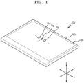
- FIG. 1 is a perspective view schematically illustrating a display device according to an embodiment.
- a display device DV may include a display area DA and a non-display area NDA outside the display area DA.
- the display device DV may provide an image in the display area DA through an array of pixels that are two-dimensionally arranged on the x-y plane.
- the pixels may include a first pixel, a second pixel, and a third pixel.
- the first pixel is a red pixel Pr
- the second pixel is a green pixel Pg
- the third pixel is a blue pixel Pb
- the red pixel Pr, the green pixel Pg, and the blue pixel Pb may be respectively areas from which red light, green light, and blue light may be emitted.
- the display device DV may provide an image by using light emitted from the pixels.
- the non-display area NDA may be an area in which no image is provided, and may entirely surround the display area DA.
- a driver or a main voltage line for providing an electrical signal or power to pixel circuits may be arranged in the non-display area NDA.
- a pad that is an area to which an electronic device or a printed circuit board may be electrically connected, may be included in the non-display area NDA.
- the display area DA may have a polygonal shape including a rectangular shape, as shown in FIG. 1 .
- the display area DA may have a rectangular shape in which a horizontal length is greater than a vertical length, a rectangular shape in which a horizontal length is less than a vertical length, or a square shape.
- the display area DA may have various shapes such as an elliptical shape and a circular shape.
- FIG. 2 is a cross-sectional view schematically illustrating pixels of a display device according to an embodiment.
- the display device DV may include a circuit layer 200 on a substrate 100.
- the circuit layer 200 may include first to third pixel circuits PC1, PC2, and PC3, and the first to third pixel circuits PC1, PC2, and PC3 may be electrically and respectively connected to first to third light emitting diodes LED1, LED2, and LED3 of a light emitting diode layer 300.
- the first to third light emitting diodes LED1, LED2, and LED3 may each include an organic light emitting diode including an organic material.
- the first to third light emitting diodes LED1, LED2, and LED3 may be inorganic light emitting diodes each including an inorganic material.
- Each of the inorganic light emitting diodes may include a p-n junction diode including materials based on an inorganic semiconductor. In the case that a voltage is applied to the p-n junction diode in a forward direction, holes and electrons may be injected, and energy generated by recombination of the holes and the electrons may be converted into light energy to emit light of a color.
- the inorganic light emitting diode described above may have a width of several to several hundreds of micrometers or several to several hundreds of nanometers.
- the light emitting diode LED may be a light emitting diode including quantum dots.
- a light emitting layer of the light emitting diode LED may include an organic material, an inorganic material, quantum dots, an organic material and quantum dots, or an inorganic material and quantum dots.
- the first to third light emitting diodes LED1, LED2, and LED3 may emit light of a same color.
- light e.g., blue light Lb
- emitted from the first to third light emitting diodes LED1, LED2, and LED3 may pass through an encapsulation layer 400 on the light emitting diode layer 300 and may pass through a color conversion-transmitting layer 500.
- the color conversion-transmitting layer 500 may include optical parts that transmit light (e.g., blue light Lb) emitted from the light emitting diode layer 300 with or without color conversion.
- the color conversion-transmitting layer 500 may include color conversion parts that convert light (e.g., blue light Lb) emitted from the light emitting diode layer 300 into light of different colors, and a transmitting part that transmits light (e.g., blue light Lb) emitted from the light emitting diode layer 300 without color conversion.
- the color conversion-transmitting layer 500 may include a first color conversion part 510 corresponding to the red pixel Pr, a second color conversion part 520 corresponding to the green pixel Pg, and a transmitting part 530 corresponding to the blue pixel Pb.
- the first color conversion part 510 may convert the blue light Lb into red light Lr
- the second color conversion part 520 may convert the blue light Lb into green light Lg.
- the transmitting part 530 may pass through the blue light Lb without conversion.
- a color layer 600 may be arranged on the color conversion-transmitting layer 500.
- the color layer 600 may include first to third color filters 610, 620, and 630 of different colors.
- the first color filter 610 may be a red color filter
- the second color filter 620 may be a green color filter
- the third color filter 630 may be a blue color filter.
- Light that is color-converted and transmitted by the color conversion-transmitting layer 500 may pass through the first to third color filters 610, 620, and 630 so that color purity may be enhanced. Also, the color layer 600 may prevent or minimize external light (e.g., light incident toward the display device DV from the outside of the display device DV) from being reflected and visually recognized by a user.
- external light e.g., light incident toward the display device DV from the outside of the display device DV
- a light-transmitting base layer 700 may be provided on the color layer 600.
- the light-transmitting base layer 700 may include glass or a light-transmitting organic material.
- the light-transmitting base layer 700 may include a light-transmitting organic material such as acryl-based resin.
- the light-transmitting base layer 700 may be a kind of substrate, and after the color layer 600 and the color conversion-transmitting layer 500 are formed on the light-transmitting base layer 700, the light-transmitting base layer 700 may be integrated so that the color conversion-transmitting layer 500 faces the encapsulation layer 400.
- the light-transmitting base layer 700 may be directly applied and cured on the color layer 600.
- another optical film for example, an anti-reflection (AR) film, may be arranged on the light-transmitting base layer 700.
- AR anti-reflection
- the display device DV having the above-described structure may include an electronic device that may display a moving image or a still image, such as a television (TV), a billboard, a cinema screen, a monitor, a tablet personal computer (PC), a laptop computer, or the like.
- a television TV
- a billboard a cinema screen
- a monitor a monitor
- a tablet personal computer PC
- laptop computer a laptop computer
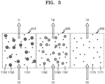
- FIG. 3 illustrates optical parts of a color conversion-transmitting layer of FIG. 2 .
- a first color conversion part 510 may convert incident blue light Lb into red light Lr.
- the first color conversion part 510 may include a first photosensitive polymer 1151, and first quantum dots 1152 and first scattering particles 1153 which are dispersed in the first photosensitive polymer 1151.
- the first quantum dots 1152 may be excited by the blue light Lb to isotropically emit the red light Lr having a longer wavelength than the blue light Lb.
- the first photosensitive polymer 1151 may be an organic material having light transmittance.
- the first scattering particles 1153 may scatter the blue light Lb that is not absorbed on the first quantum dots 1152 so that more first quantum dots 1152 may be excited. Thus, color conversion efficiency may be increased.
- the first scattering particles 1153 may be, for example, titanium oxide (TiO 2 ) or metal particles.
- the first quantum dots 1152 may be selected from the group consisting of a group II-VI compound, a group III-V compound, a group IV-VI compound, a group-IV element, a group-IV compound, and a combination thereof.
- the second color conversion part 520 may convert the incident blue light Lb into green light Lg.
- the second color conversion part 520 may include a second photosensitive polymer 1161, and second quantum dots 1162 and second scattering particles 1163 which are dispersed in the second photosensitive polymer 1161.
- the second quantum dots 1162 may be excited by the blue light Lb to isotropically emit the green light Lg having a longer wavelength than the blue light Lb.
- the second photosensitive polymer 1161 may be an organic material having light transmittance.
- the second scattering particles 1163 may scatter the blue light Lb that is not absorbed on the second quantum dots 1162, so that more second quantum dots 1162 may be excited. Thus, color conversion efficiency may be increased.
- the second scattering particles 1163 may be, for example, titanium oxide (TiO 2 ) or metal particles.
- the second quantum dots 1162 may be selected from the group consisting of a group II-VI compound, a group III-V compound, a group IV-VI compound, a group-IV element, a group-IV compound, and a combination thereof.
- the transmitting part 530 may transmit the blue light Lb without converting the blue light Lb that is incident on the transmitting part 530.
- the transmitting part 530 may include a third photosensitive polymer 1171 in which third scattering particles 1173 are dispersed, as shown in FIG. 3 .
- the third photosensitive polymer 1171 may be an organic material having light transmittance, such as silicon resin or epoxy resin, and the third photosensitive polymer 1171 and the first and second photosensitive polymers 1151 and 1161 may include a same material.
- the third scattering particles 1173 may scatter and emit the blue light Lb, and the third scattering particles 1173 and the first and second scattering particles 1153 and 1163 may include a same material.
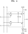
- FIG. 4 is a schematic diagram of an equivalent circuit of a light emitting diode and a pixel circuit electrically connected to the light emitting diode of a display device according to an embodiment.
- a pixel circuit PC shown in FIG. 4 may correspond to each of the first to third pixel circuits PC1, PC2, and PC3, and the light emitting diode of FIG. 4 may correspond to each of the first to third light emitting diodes LED1, LED2, and LED3 described above with reference to FIG. 2 .
- a first electrode (e.g., an anode) of a light emitting diode for example, an organic light emitting diode OLED
- a second electrode (e.g., a cathode) of the organic light emitting diode OLED may be electrically connected to an auxiliary wiring 240 for providing a common voltage ELVSS.
- the organic light emitting diode OLED may emit light with brightness corresponding to the amount of current supplied from the pixel circuit PC.
- the organic light emitting diode OLED of FIG. 4 may correspond to each of the first to third light emitting diodes LED1, LED2, and LED3 shown in FIG. 2 described above, and the pixel circuit PC of FIG. 4 may correspond to each of the first to third pixel circuits PC1, PC2, and PC3 shown in FIG. 2 described above.
- the pixel circuit PC may control the amount of current that flows from a driving voltage line 250 for providing a driving voltage ELVDD to the auxiliary wiring 240 via the organic light emitting diode OLED in response to a data signal.
- the pixel circuit PC may include a first transistor M1, a second transistor M2, a third transistor M3, and a storage capacitor Cst.
- Each of the first transistor M1, the second transistor M2, and the third transistor M3 may be an oxide semiconductor transistor including a semiconductor layer including an oxide semiconductor, or a silicon semiconductor transistor including a semiconductor layer including polysilicon.
- the first electrode may be one of a source electrode and a drain electrode
- the second electrode may be the other of the source electrode and the drain electrode.
- a first electrode of the first transistor M1 may be connected to a driving voltage line 250 for providing the driving voltage ELVDD, and a second electrode of the first transistor M1 may be connected to the first electrode of the organic light emitting diode OLED.
- a gate electrode of the first transistor M1 may be electrically connected to a first node N1. The first transistor M1 may control the amount of current that flows from the driving voltage line 250 to the organic light emitting diode OLED in response to a voltage of the first node N1.
- the second transistor M2 may be a switching transistor.
- a first electrode of the second transistor M2 may be connected to a data line DL, and a second electrode of the second transistor M2 may be connected to the first node N1.
- a gate electrode of the second transistor M2 may be connected to a scan line SL. In the case that a scan signal is supplied to the scan line SL, the second transistor M2 may be turned on to electrically connect the data line DL to the first node N1.
- the third transistor M3 may be an initialization transistor and/or a sensing transistor.
- a first electrode of the third transistor M3 may be connected to a second node N2, and a second electrode of the third transistor M3 may be connected to a sensing line SL.
- a gate electrode of the third transistor M3 may be electrically connected to a control line CL.
- the storage capacitor Cst may be connected between the first node N1 and the second node N2.
- a first capacitor electrode of the storage capacitor Cst may be connected to the gate electrode of the first transistor M1
- a second capacitor electrode of the storage capacitor Cst may be connected to the first electrode of the organic light emitting diode OLED.
- FIG. 4 illustrates that the first transistor M1, the second transistor M2, and the third transistor M3 are N-channel metal oxide semiconductor (NMOS) transistors.
- NMOS metal oxide semiconductor
- embodiments are not limited thereto.
- at least one of the first transistor M1, the second transistor M2, and the third transistor M3 may be a P-channel metal oxide semiconductor (PMOS) transistor.
- PMOS P-channel metal oxide semiconductor
- FIG. 4 illustrates three transistors. However, embodiments are not limited thereto.
- the pixel circuit PC may include four or more transistors.
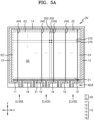
- FIG. 5A is a plan view illustrating a common voltage supply line and a driving voltage supply line of a display device according to an embodiment.
- a display device DV may include a common voltage supply line 10 for supplying a common voltage ELVSS to the second electrode of the organic light emitting diode OLED described above with reference to FIG. 4 , and a driving voltage supply line 20 for supplying a driving voltage ELVDD to the pixel circuit PC.
- the common voltage supply line 10 and the driving voltage supply line 20 may be arranged in the non-display area NDA.
- the display device DV and the substrate 100 may have substantially a same shape.
- the substrate 100 may include the display area DA and the non-display area NDA outside the display area DA.
- the substrate 100 includes the display area DA and the non-display area NDA outside the display area DA.
- the common voltage supply line 10 may include a first common voltage input part 11 and a second common voltage input part 12 which are arranged adjacent to a first edge E1 of the display area DA.
- the first common voltage input part 11 and the second common voltage input part 12 may be apart from each other in an x direction and may be integrally connected to each other through first to third extension portions 13, 14, and 15 which are arranged adjacent to second to fourth edges E2, E3 and E4 of the display area DA, respectively.
- At least one third common voltage input part 16 may be arranged between the first common voltage input part 11 and the second common voltage input part 12.
- FIG. 5A illustrates four third common voltage input parts 16.
- the common voltage supply line 10 may be electrically connected to the auxiliary wirings 240 that pass through the display area DA.
- Each of the auxiliary wirings 240 may extend in a y direction, for example, as shown in FIG. 5A .
- At least one auxiliary wiring 240 may extend across the display area DA in the y direction and may be electrically connected to the first common voltage input part 11 and a portion of the second extension portion 14 facing the first common voltage input part 11.
- At least another auxiliary wiring 240 may extend across the display area DA in the y direction and may be electrically connected to the second common voltage input part 12 and a portion of the second extension portion 14 facing the second common voltage input part 12.
- at least another auxiliary wiring 240 may extend across the display area DA in the y direction and may be electrically connected to the third common voltage input part 16 and a portion of the second extension portion 14 facing the third common voltage input part 16.
- the common voltage supply line 10 further includes the third common voltage input part 16 arranged between the first common voltage input part 11 and the second common voltage input part 12, current density may be reduced, and heat generation may be suppressed in the case that current supplied through the common voltage supply line 10 is applied, compared to the case where the common voltage supply line 10 includes only the first common voltage input part 11 and the second common voltage input part 12.
- the driving voltage supply line 20 may be located in the non-display area NDA and may include a driving voltage supply part 21 that is adjacent to the first edge E1 of the display area DA, and a counterpart 22 that extends along the third edge E3 of the display area DA.
- the driving voltage supply part 21 and the counterpart 22 may be arranged at both sides of the display area DA with the display area DA therebetween.
- the driving voltage supply line 20 may be electrically connected to driving voltage lines 250 intersecting the display area DA. Each of the driving voltage lines 250 may extend in the y direction while being electrically connected to the driving voltage supply part 21. In some embodiments, the driving voltage lines 250 may be electrically connected to horizontal driving voltage lines 270 that extend in the x direction to intersect the driving voltage lines 250. The driving voltage lines 250 and the horizontal driving voltage lines 270 may be arranged on different layers and may be electrically connected to each other via a contact hole passing through at least one insulating layer therebetween.
- FIGS. 5B and 5C are plan views illustrating a common voltage supply line of a display device according to other embodiments, respectively.
- the display device DV shown in FIGS. 5B and 5C may include the driving voltage line 250 (see FIG. 5A ) and the horizontal driving voltage line 270 (see FIG. 5A ) that are electrically connected to the driving voltage supply line 20, as described above with reference to FIG. 5A .
- the driving voltage line 250 (see FIG. 5A ) and the horizontal driving voltage line 270 (see FIG. 5A ) are omitted from FIGS. 5B and 5C .
- the display device DV may include an auxiliary wiring 240' (hereinafter referred to as a first auxiliary wiring) intersecting the display area DA in the y direction and an auxiliary wiring 240" (hereinafter referred to as a second auxiliary wiring) intersecting the display area DA in the x direction.
- the first auxiliary wiring 240' and the second auxiliary wiring 240" that intersect each other may be arranged on different layers and may be electrically connected to each other via a through hole formed in at least one insulating layer therebetween.
- FIGS. 5A and 5B illustrate that the first common voltage input part 11 and the second common voltage input part 12 of the common voltage supply line 10 are integrally and electrically connected to each other by the first to third extension portions 13, 14, and 15.
- embodiments are not limited thereto.
- the common voltage supply line 10 may include a first common voltage input part 11 and a second common voltage input part 12 which are arranged adjacent to the first edge E1 of the display area DA, and an extension portion 14' that is arranged adjacent to the third edge E3 of the display area DA.
- the extension portion 14' may be physically separated from the first common voltage input part 11 and the second common voltage input part 12.
- each of the auxiliary wirings 240 may be electrically connected to the first to third common voltage input parts 11, 12, or 16, and the other end of each of the auxiliary wirings 240 may be electrically connected to the extension portion 14'.
- the first to third common voltage input parts 11, 12, and 16 and the extension portion 14' are electrically connected to each other by the auxiliary wirings 240 intersecting the display area DA, the first extension portion 13 and the third extension portion 15 may be omitted, as shown in FIGS. 5A and 5B as described above.
- the first extension portion 13 and the third extension portion 15 are omitted so that a portion (e.g., a portion of the non-display area NDA adjacent to the second edge E2 and the fourth edge E4 of the display area DA) of the non-display area NDA may be reduced.
- FIG. 6 is a cross-sectional view illustrating a portion of a display device according to an embodiment
- FIG. 7 is an enlarged cross-sectional view of region VI of FIG. 6
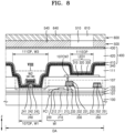
- FIG. 8 is a cross-sectional view illustrating a portion of a display device according to an embodiment
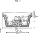
- FIG. 9 is an enlarged cross-sectional view of region VIII of FIG. 8 .
- FIGS. 10A and 10B are cross-sectional views illustrating an auxiliary wiring according to other embodiments, respectively.
- auxiliary wirings 240, 240', and 240" described above with reference to FIGS. 5A to 5C may be electrically connected to the second electrode of the light emitting diode LED in the display area DA.
- the auxiliary wiring 240 shown in FIG. 5A or 5C is electrically connected to the second electrode of the light emitting diode LED.
- the first auxiliary wiring 240' and/or the second auxiliary wiring 240" described with reference to FIG. 5B may be electrically connected to the second electrode of the light emitting diode LED.
- the auxiliary wiring 240 shown in FIG. 6 may be the first auxiliary wiring 240' and/or the second auxiliary wiring 240" described with reference to FIG. 5B .
- FIG. 6 illustrates a first light emitting diode LED1 among light emitting diodes arranged in a display device.
- the second and third light emitting diodes LED2 and LED3 described above with reference to FIG. 2 and the first light emitting diode LED1 of FIG. 6 have a same structure.
- the first light emitting diode LED1 may be arranged on the substrate 100.
- a first pixel circuit PC1 electrically connected to the first light emitting diode LED1 may be arranged between the substrate 100 and the first light emitting diode LED1.
- the first pixel circuit PC1 may include transistors and a storage capacitor, as described above with reference to FIG. 4 .
- FIG. 6 illustrates a first transistor M1.
- the substrate 100 may include a glass material or polymer resin.
- the substrate 100 including polymer resin may be flexible.
- the shape of the display device including the substrate 100 that is flexible may be changed to be curved, bendable, rollable, or foldable.
- a buffer layer 101 may be arranged on the substrate 100 and may prevent impurities from penetrating from the substrate 100 into a transistor, for example, the first transistor M1.
- the buffer layer 101 may include an inorganic insulating material such as silicon oxide, silicon nitride, and/or silicon oxynitride.
- a driving semiconductor layer 210 of the first transistor M1 may be arranged on the buffer layer 101.
- the driving semiconductor layer 210 may include an oxide semiconductor.
- the oxide semiconductor may include indium gallium zinc oxide (IGZO), zinc tin oxide (ZTO), indium zinc oxide (IZO), or the like.
- the driving semiconductor layer 210 may include polysilicon, amorphous silicon, an organic semiconductor, or the like.
- the driving semiconductor layer 210 may include a channel region 211 that overlaps a driving gate electrode 220, and a first region 212 and a second region 213 which are disposed at both sides of the channel region 211 and doped or conducted with impurities.
- One of the first region 212 and the second region 213 may correspond to a source region, and the other one thereof may correspond to a drain region.
- the driving gate electrode 220 may overlap the channel region 211 of the driving semiconductor layer 210 with a gate insulating layer 103 therebetween.
- the driving gate electrode 220 may include a conductive material including molybdenum (Mo), aluminium (Al), copper (Cu), titanium (Ti), or the like, and may have a single-layered or multi-layered structure including the above-described materials.
- the gate insulating layer 103 may include an inorganic insulating material such as silicon oxide, silicon nitride, and/or silicon oxynitride.
- An electrode 230 may be arranged on an interlayer insulating layer 105 and may be electrically connected to one of the first region 212 and the second region 213 of the driving semiconductor layer 210.
- FIG. 6 illustrates that the electrode 230 is electrically connected to the second region 213.
- the electrode 230 may correspond to a source (or drain) electrode.
- the interlayer insulating layer 105 may include an inorganic insulating material such as silicon oxide, silicon nitride, and/or silicon oxynitride.
- the driving voltage line 250 may be arranged on the electrode 230, and the driving voltage line 250 and the electrode 230 may be formed together by a same process.
- the electrode 230 and the driving voltage line 250 may include sub-layers.
- the electrode 230 may include a first layer 231, a second layer 232 under the first layer 231, and a third layer 233 under the second layer 232.
- the driving voltage line 250 may include a first layer 251, a second layer 252 under the first layer 251, and a third layer 253 under the second layer 252.
- the auxiliary wiring 240 arranged in the display area DA may be arranged adjacent to the first pixel circuit PC1.
- the auxiliary wiring 240, and the electrode 230 and/or the driving voltage line 250 may be arranged on a same layer.
- FIG. 6 illustrates that the auxiliary wiring 240 is arranged on the interlayer insulating layer 105.
- the auxiliary wiring 240 may have a stack structure including conductive layers.
- the auxiliary wiring 240 may include a main sub-layer 242, an upper layer 241 on the main sub-layer 242, and a lower layer 243 under the main sub-layer 242.
- the main sub-layer 242 may be a sub-layer that occupies most of the auxiliary wiring 240.
- the fact that the main sub-layer 242 occupies most of the auxiliary wiring 240 may indicate that a thickness t2 of the main sub-layer 242 is about 50% of a total thickness Tp of the auxiliary wiring 240.
- the thickness t2 of the main sub-layer 242 may be about 60% or more or about 70% or more of the total thickness Tp of the auxiliary wiring 240.
- the thickness t2 of the main sub-layer 242 may be greater than the thickness of each of the upper layer 241 and the lower layer 243. In an embodiment, the thickness t2 of the main sub-layer 242 may be about 1000 ⁇ to about 15000 ⁇ .
- the main sub-layer 242 may include Cu, Al, platinum (Pt), palladium (Pd), silver (Ag), magnesium (Mg), gold (Au), nickel (Ni), neodymium (Nd), iridium (Ir), chromium (Cr), lithium (Li), calcium (Ca), and/or Mo.
- the main sub-layer 242 may have a single-layered or multi-layered structure including the above-described materials.
- the main sub-layer 242 may be a single layer including Cu or a single layer including Al.
- the lower layer 243 may include a different material from the main sub-layer 242.
- the lower layer 243 may be selected considering conductivity and adhesion.
- the lower layer 243 may include a metal layer including metal such as titanium (Ti) or transparent conductive oxide (TCO) such as gallium zinc oxide (GZO) and/or IZO, and the TCO described above may be an amorphous or crystalline material.
- the upper layer 241 may be arranged on the main sub-layer 242 and may include a different material from the main sub-layer 242.
- the upper layer 241 may prevent the main sub-layer 242 from being damaged during a process of manufacturing the display device.
- the upper layer 241 may include TCO such as ITO.
- the upper layer 241 may include metal such as Ti, Mo, and/or tungsten (W).
- the upper layer 241 may have a multi-layered structure including the above-described metal layer and a TCO layer.
- the electrode 230 and the driving voltage line 250 arranged on the same layer as the auxiliary wiring 240, and the auxiliary wiring 240 may include a same material.
- the first layer 231, the second layer 232, and the third layer 233 of the electrode 230 and the upper layer 241, the main sub-layer 242, and the lower layer 243 of the auxiliary wiring 240 may include a same material, respectively.
- the first layer 251, the second layer 252, and the third layer 253 of the driving voltage line 250 and the upper layer 241, the main sub-layer 242, and the lower layer 243 of the auxiliary wiring 240 may include a same material, respectively.
- a planarization insulating layer 107 may be arranged on the electrode 230, the auxiliary wiring 240, and the driving voltage line 250.
- the planarization insulating layer 107 may include an organic insulating material such as acryl, benzocyclobutene (BCB), polyimide, and/or hexamethyldisiloxane (HMDSO).
- the planarization insulating layer 107 may include a first opening 107OP that overlaps the auxiliary wiring 240.
- a first width W1 of the first opening 107OP may be greater than a second width W2 of the auxiliary wiring 240.
- a portion of an upper surface of an insulating layer, for example, the interlayer insulating layer 105 under the planarization insulating layer 107, may be exposed through the first opening 107OP.
- a first electrode 310 on the planarization insulating layer 107 may be electrically connected to the first pixel circuit PC1 through a contact hole 107CNT.
- the first electrode 310 may be electrically connected to the electrode 230 through the contact hole 107CNT.
- the first electrode 310 may include TCO such as ITO, IZO, ZnO, In 2 O 3 , IGO or AZO.
- the first electrode 310 may include a reflective layer including Ag, Mg, Al, Pt, Pd, Au, Ni, Nd, Ir, Cr, or a compound thereof.
- the first electrode 310 may further include a layer formed of ITO, IZO or In 2 O 3 on/under the above-described reflective layer.
- the first electrode 310 may have a three-layer structure in which an ITO layer, an Ag layer and an ITO layer are stacked.
- a bank layer 111 may be arranged on the first electrode 310 and may cover (or overlap in a plan view) edges of the first electrode 310.
- the bank layer 111 may include an opening (hereinafter referred to as an emission opening 111EOP) that overlaps a portion of the first electrode 310.
- a central portion of the first electrode 310 may be exposed through the emission opening 111EOP.
- the bank layer 111 may include an organic material.
- the bank layer 111 may include a second opening 111OP that overlaps the first opening 107OP of the planarization insulating layer 107.
- a third width W3 of the second opening 111OP may be greater than the first width W1 of the first opening 107OP.
- An intermediate layer 320 may contact (or be in contact with) the first electrode 310 through the emission opening 111EOP.
- the intermediate layer 320 may include an emission layer 322, as shown in FIG. 7 , and may include a functional layer located under and/or on the emission layer 322.
- FIG. 7 illustrates that the intermediate layer 320 includes a first functional layer 321 under the emission layer 322 and a second functional layer 323 on the emission layer 322.
- the first functional layer 321 may have a single or multi-layered structure.
- the first functional layer 321 may include a hole injection layer (HIL) and/or a hole transport layer (HTL).
- the emission layer 322 may include a polymer or small (or high or low) molecular weight organic material that emits light of a color.
- the second functional layer 323 may include an electron transport layer (ETL) and/or an electron injection layer (EIL).
- a second electrode 330 may include a conductive material having a low work function.
- the second electrode 330 may include a (semi-)transparent layer including Ag, Mg, Al, Pt, Pd, Au, Ni, Nd, Ir, Cr, Li, Ca, or an alloy thereof.
- the second electrode 330 may further include a layer such as ITO, IZO, ZnO, or In 2 O 3 on the (semi-)transparent layer including the above-described materials.
- the intermediate layer 320 and the second electrode 330 may be deposited by using a mask having an opening corresponding to the display area DA.
- the intermediate layer 320 may have the same area as the total area of the display area DA in a plan view and may be electrically disconnected or separated from the auxiliary wiring 240 by the shape of the auxiliary wiring 240.
- the second electrode 330 may have the same area as the total area of the display area DA in the plan view and may be electrically disconnected or separated from the auxiliary wiring 240 by the shape of the auxiliary wiring 240. Portions of the second electrode 330 located outside the auxiliary wiring 240 may contact a side surface of the auxiliary wiring 240. Similarly, portions of the intermediate layer 320 located outside the auxiliary wiring 240 may contact the side surface of the auxiliary wiring 240.
- An auxiliary layer 340 may include a conductive material.
- the auxiliary layer 340 may include Ag, Mg, Al, Pt, Pd, Au, Ni, Nd, Ir, Cr, Li, Ca, or Mo.
- the auxiliary layer 340 may include conductive oxide.
- the auxiliary layer 340 may include TCO such as ITO, GZO, and/or IZO, and the above-described TCO may be an amorphous or crystalline material.
- the auxiliary layer 340 may have a single-layered or multi-layered structure including the above-described materials.
- the auxiliary layer 340 may have a composite structure in which a metal layer and a conductive oxide layer are stacked.
- the auxiliary layer 340 may be a layer having conductivity and may be arranged on the second electrode 330.
- the auxiliary layer 340 may be deposited by using a mask having an opening corresponding to a region in which the auxiliary wiring 240 and the first opening 107OP of the display area DA are formed.
- a fourth width W4 of the auxiliary layer 340 may be greater than the second width W2 of the auxiliary wiring 240 and may be less than the first width W1 of the first opening 107OP.
- the auxiliary layer 340 may be deposited by using a mask having an opening corresponding to the display area DA.
- the auxiliary layer 340 may have the same area as the total area of the display area DA in the plan view beyond the region in which the first opening 107OP is formed.
- the auxiliary layer 340 may overlap the auxiliary wiring 240 and the first opening 107OP, and the auxiliary layer 340 and the second electrode 330 may have a same area in the plan view beyond the first opening 107OP.
- the auxiliary layer 340 may be electrically disconnected or separated from the auxiliary wiring 240. Portions of the auxiliary layer 340 located outside the auxiliary wiring 240 may contact the side surface of the auxiliary wiring 240.
- the auxiliary layer 340 may be a conductive layer, and may be directly arranged on an upper surface of the second electrode 330 and may contact the side surface of the auxiliary wiring 240 so that a contact resistance between the second electrode 330 and the auxiliary wiring 240 may be reduced. Also, the contact resistance between the second electrode 330 and the auxiliary wiring 240 may be reduced by using the auxiliary layer 340 so that the thickness of the second electrode 330 may be maintained to be thin.
- the auxiliary wiring 240 may be formed so that the width of the upper layer 241 on the main sub-layer 242 may be greater than the width of an upper surface 242t of the main sub-layer 242, as shown in FIG. 7 .
- the upper layer 241 may include a tip T protruding from a part where a side surface 242s and an upper surface 242t of the main sub-layer 242 meet each other.
- Such a structure may be formed in a process of etching a portion of the auxiliary wiring 240 exposed through the first opening 107OP, for example, in an etching process using an etchant in a process of forming the first electrode 310.
- a material of the main sub-layer 242 may include a material having a different etching selectivity from a material of the upper layer 241.
- a material of the lower layer 243 may include a material having a different etching selectivity from the material of the main sub-layer 242.
- the lower layer 243 and the upper layer 241 may include a same material.
- the main sub-layer 242 is overetched compared to the upper layer 241 by the etchant used in the etching process, so that a structure having the tip T, as shown in FIGS. 6 and 7 , may be formed.
- the auxiliary wiring 240 comprises the structure having the tip.
- the intermediate layer 320, the second electrode 330, and the auxiliary layer 340 may be deposited in a direction (z direction) perpendicular to the substrate 100 and an oblique direction thereto.
- the intermediate layer 320, the second electrode 330, and the auxiliary layer 340 may be electrically disconnected by the tip structure of the auxiliary wiring 240.
- a portion 320R of the intermediate layer 320 may be located on an upper surface of the auxiliary wiring 240, and the other portion of the intermediate layer 320 adjacent to the auxiliary wiring 240 may directly contact a side surface 242s of the main sub-layer 242.
- a portion 330R of the second electrode 330 may be located on an upper surface of the intermediate layer 320 located on the upper surface of the auxiliary wiring 240, and the other portion of the second electrode 330 adjacent to the auxiliary wiring 240 may directly contact the side surface 242s of the main sub-layer 242 to form a first contact region CCR.
- a portion 340R of the auxiliary layer 340 may be located on an upper surface of the second electrode 330, located on the upper surface 240t of the auxiliary wiring 240, and the other portion of the auxiliary layer 340 adjacent to the auxiliary wiring 240 may directly contact the side surface 242s of the main sub-layer 242 to form a second contact region CR.
- each of the first functional layer 321, the emission layer 322, and the second functional layer 323 may be electrically disconnected from the auxiliary wiring 240.
- each of the first functional layer 321, the emission layer 322, and the second functional layer 323 may include a portion outside the auxiliary wiring 240, and portions 321R, 322R, and 323R located on the upper surface 240t of the auxiliary wiring 240.
- an inclination angle ⁇ of the side surface 242s of the main sub-layer 242 may be greater than or equal to about 20° and less than about 90°.
- FIGS. 6 and 7 illustrate that the side surface 242s of the main sub-layer 242 has a tapered shape in a forward direction.
- the inclination angle ⁇ of the side surface 242s of the main sub-layer 242 may be about 90°.
- the inclination angle ⁇ of the side surface 242s of the main sub-layer 242 may be greater than about 90° and less than or equal to about 135°.
- a light emitting diode including a multi-layered structure of the first electrode 310, the intermediate layer 320, and the second electrode 330, for example, a first light emitting diode LED1 may be covered by the encapsulation layer 400.
- the encapsulation layer 400 may include at least one inorganic encapsulation layer and at least one organic encapsulation layer.
- the encapsulation layer 400 may include a first inorganic encapsulation layer 410, an organic encapsulation layer 420, and a second inorganic encapsulation layer 430 which are sequentially stacked.
- Each of the first and second inorganic encapsulation layers 410 and 430 may include one or more inorganic insulating materials.
- the inorganic insulating materials may include aluminium oxide, tantalum oxide, hafnium oxide, zinc oxide, silicon oxide, silicon nitride, and/or silicon oxynitride.
- the first and second inorganic encapsulation layers 410 and 430 may be formed by chemical vapor deposition. Because the first inorganic encapsulation layer 410 has a relatively high step coverage, although the auxiliary wiring 240 has the tip T (see FIG. 7 ), the auxiliary wiring 240 may be entirely covered.
- the first inorganic encapsulation layer 410 may consecutively extend to cover the portions of the intermediate layer 320, the second electrode 330, and the auxiliary layer 340 disposed outside the auxiliary wiring 240, a portion of the side surface 242s of the main sub-layer 242, a lower surface and a side surface of the upper layer 245, a portion 320R of the intermediate layer 320, a portion 330R of the second electrode 330, and a portion 340R of the auxiliary layer 340 on the auxiliary wiring 240.
- the organic encapsulation layer 420 may include a polymer-based material.
- the polymer-based material may include acryl-based resin, epoxy-based resin, polyimide, polyethylene, and the like.
- the acryl-based resin may include, for example, polymethylmethacrylate, polyacrylic acid, or the like.
- the color-conversion transmitting layer 500 and the color layer 600 may be arranged on the encapsulation layer 400.
- FIG. 6 illustrates that the first color conversion part 510 of the color conversion-transmitting layer 500 is disposed to overlap the first light emitting diode LED1 and the first color filter 610 of the color layer 600 is disposed to overlap the first light emitting diode LED1.
- Each of the first color conversion part 510 and the first color filter 610 may be surrounded by light shielding parts 540 and 640.
- FIG. 6 illustrates the light shielding parts 540 and 640 arranged at both sides of each of the first color conversion part 510 and the first color filter 610.
- the light shielding parts 540 and 640 may include a light shielding material such as a black matrix, and the auxiliary wiring 240 may overlap the light shielding parts 540 and 640.
- FIG. 11A is a perspective view schematically illustrating an auxiliary wiring and a first opening of a planarization insulating layer on the auxiliary wiring according to an embodiment
- FIG. 11B is a plan view schematically illustrating FIG. 11A .
- the first width W1 of the first opening 107OP of the planarization insulating layer 107 may be greater than the second width W2 of a portion of the auxiliary wiring 240 that overlaps the first opening 107OP.
- a portion of the auxiliary wiring 240 overlapping a material portion of the planarization insulating layer 107 may be formed so that the upper layer 241, the main sub-layer 242, and the lower layer 243 may have comparatively a same width.
- the portion of the auxiliary wiring 240 overlapping the first opening 107OP is etched by the etchant, as described above, the cross-sectional shapes of the upper layer 241, the main sub-layer 242, and the lower layer 243 may have the structure described above with reference to FIGS. 6 and 7 (or FIGS. 10A and 10B ).
- the size or the area of the main sub-layer 242 overlapping the first opening 107OP may be relatively less than the size or the area of the upper layer 241.
- a solid line indicates an outline (which corresponds to a side surface in a cross-sectional view) of the upper layer 241 and/or the lower layer 243 in a plan view
- a dotted line indicates an outline (which corresponds to a side surface in the cross-sectional view) of the main sub-layer 242 in the plan view.
- the width of the upper layer 241 and/or the lower layer 243 may correspond to the second width W2, and a width W22 of the main sub-layer 242 may be less than a width (e.g., the second width W2) of the upper layer 241 and/or the lower layer 243.
- a dotted line portion overlapping the first opening 107OP corresponds to a first contact region CCR (see FIG. 7 ) in which the auxiliary wiring 240 and the second electrode 330 described above with reference to FIGS. 7 and 8 directly contact each other, or a second contact region CR (see FIG. 7 ) in which the auxiliary wiring 240 and the auxiliary layer 340 directly contact each other.
- FIGS. 11A and 11B illustrate that the auxiliary wiring 240 overlapping the first opening 107OP has a comparatively uniform width in the x direction.
- the auxiliary wiring 240 may include a protrusion that protrudes in a direction (e.g., the x direction) intersecting an extension direction (e.g., the y direction) of the auxiliary wiring 240.
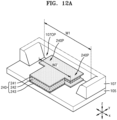
- FIG. 12A is a perspective view schematically illustrating an auxiliary wiring and a first opening of a planarization insulating layer on the auxiliary wiring according to an embodiment
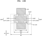
- FIG. 12B is a plan view illustrating an auxiliary wiring and a first opening of a planarization insulating layer according to an embodiment
- FIG. 12C is a plan view illustrating an auxiliary wiring and a first opening of a planarization insulating layer according to an embodiment.
- the auxiliary wiring 240 may include a protrusion 240P that protrudes in a direction (e.g., the x direction) intersecting the extension direction (e.g., the y direction) of the auxiliary wiring 240.
- protrusions 240P may be arranged on both sides of the auxiliary wiring 240.
- FIGS. 12A and 12B illustrate that the auxiliary wiring 240 includes a pair of protrusions 240P.
- the auxiliary wiring 240 may include pairs of protrusions 240P, as shown in FIG. 12C .
- auxiliary wiring 240 includes the protrusions 240P, the upper layer 241, the main sub-layer 242, and the lower layer 243 included in the auxiliary wiring 240 may include protrusions 241P, 242P, and 243P, respectively.
- the protrusions 240P of the auxiliary wiring 240 may overlap the first opening 107OP of the planarization insulating layer 107, and the first width W1 of the first opening 107OP may be greater than a second width W2' of a portion of the auxiliary wiring 240 overlapping the first opening 107OP.
- the second width W2' may correspond to a maximum width of a portion of the auxiliary wiring 240 overlapping the first opening 107OP.
- the second width W2' may correspond to a distance from an end of a protrusion 240P to an end of another protrusion 240P.
- a portion of the auxiliary wiring 240 overlapping (e.g., in a plan view) the first opening 107OP is etched by the etchant, as described above, and thus the cross-sectional shape of the upper layer 241, the main sub-layer 242, and the lower layer 243 may have the structure described above with reference to FIGS. 6 and 7 (or FIGS. 10A and 10B ). In this regard, as illustrated in FIGS.
- a solid line indicates an outline (which corresponds to a side surface in a cross-sectional view) of the upper layer 241 and/or the lower layer 243 in a plan view
- a dotted line indicates an outline (which corresponds to a side surface in the cross-sectional view) of the main sub-layer 242 in the plan view.
- the width of the upper layer 241 and/or the lower layer 243 may correspond to the second width W2'
- a width W22' of the main sub-layer 242 may be less than a width (e.g., the second width W2') of the upper layer 241 and/or the lower layer 243.
- a dotted line portion overlapping the first opening 107OP corresponds to a first contact region CCR (see FIG. 7 ) in which the auxiliary wiring 240 and the second electrode 330 described above with reference to FIG. 7 directly contact each other, or a second contact region CR (see FIG. 7 ) in which the auxiliary wiring 240 and the auxiliary layer 340 directly contact each other.
- the first contact region CCR of the second electrode 330 and a side surface of the auxiliary wiring 240 (e.g., a side surface of the main sub-layer 242) or the second contact region CR of the auxiliary layer 340 and a side surface of the auxiliary wiring 240 (e.g., a side surface of the main sub-layer 242) may be continuous along at least one side surface of the protrusions 240P of the auxiliary wiring 240.
- the auxiliary wiring 240 includes the protrusions 240P
- the contact area of the auxiliary wiring 240 and the second electrode 330 and the contact area of the auxiliary wiring 240 and the auxiliary layer 340 may be increased.
Landscapes
- Engineering & Computer Science (AREA)
- Microelectronics & Electronic Packaging (AREA)
- Devices For Indicating Variable Information By Combining Individual Elements (AREA)
- Electroluminescent Light Sources (AREA)
Abstract
Description
- One or more embodiments relate to a display device.
- In general, in display devices such as organic light emitting display devices, transistors are arranged in a display area so as to control the brightness of a light emitting diode. These transistors control a corresponding light emitting diode to emit light of a certain color by using a transmitted data signal, a driving voltage, and a common voltage.
- A certain voltage may be applied to one of electrodes of the light emitting diode through the transistor, and a voltage may be applied to the other one of the electrodes of the light emitting diode through an auxiliary wiring.
- As the ratio of a display area, in which an image may be provided, of a display device increases, a non-display area, as a dead space in which no light emitting diodes are arranged, needs to be reduced. As a space, in which components arranged in the non-display area are located, is decreased, the quality of light emitted from light emitting diodes may be lowered.
- One or more embodiments include a display device in which the area of a dead space may be reduced and a high quality image may be displayed. However, these objectives are examples, and the scope of the disclosure is not limited thereby.
- According to one or more embodiments, a display device includes an auxiliary wiring located on a substrate, an insulating layer arranged on the auxiliary wiring, overlapping the auxiliary wiring in a plan view, and including an opening having a width greater than a width of the auxiliary wiring, a first electrode located on the insulating layer, a bank layer including an emission opening that overlaps the first electrode in the plan view, an intermediate layer overlapping the first electrode through an emission opening in the plan view and including an emission layer, a second electrode located on the intermediate layer, and an auxiliary layer arranged on the second electrode. The auxiliary wiring includes sub-layers, and each of the second electrode and the auxiliary layer contacts a side surface of one of sub-layers through the opening of the insulating layer.
- The sub-layers of the auxiliary wiring may include a main sub-layer, an upper layer arranged on the main sub-layer and having a tip protruding from a part in which a side surface and an upper surface of the main sub-layer meet each other, and a lower layer arranged under the main sub-layer. Each of the second electrode and the auxiliary layer may directly contact the side surface of the main sub-layer.
- According to an embodiment having the above-described configuration, a display device in which a display quality may be enhanced and the area of a dead space around a display area may be reduced, may be provided. The scope of the disclosure is not limited by these effects.
-
-
FIG. 1 is a perspective view schematically illustrating a display device according to an embodiment; -
FIG. 2 is a cross-sectional view schematically illustrating pixels of a display device according to an embodiment; -
FIG. 3 illustrates optical parts of a color conversion-transmitting layer ofFIG. 2 ; -
FIG. 4 is an equivalent circuit of a light emitting diode and a pixel circuit electrically connected to the light emitting diode of a display device according to an embodiment; -
FIG. 5A is a plan view illustrating a common voltage supply line and a driving voltage supply line of a display device according to an embodiment; -
FIGS. 5B and5C are plan views illustrating a common voltage supply line of a display device according to another embodiment; -
FIG. 6 is a cross-sectional view illustrating a portion of a display device according to an embodiment; -
FIG. 7 is an enlarged cross-sectional view of region VI ofFIG. 6 ; -
FIG. 8 is a cross-sectional view illustrating a portion of a display device according to another embodiment; -
FIG. 9 is an enlarged cross-sectional view of region VIII ofFIG. 8 ; -
FIGS. 10A and10B are cross-sectional views illustrating an auxiliary wiring according to other embodiments, respectively; -
FIG. 11A is a perspective view schematically illustrating an auxiliary wiring and a first opening of a planarization insulating layer on the auxiliary wiring according to an embodiment; -
FIG. 11B is a plan view schematically illustratingFIG. 11A ; -
FIG. 12A is a perspective view schematically illustrating an auxiliary wiring and a first opening of a planarization insulating layer on the auxiliary wiring according to another embodiment; -
FIG. 12B is a plan view illustrating an auxiliary wiring and a first opening of a planarization insulating layer according to another embodiment, which is a plan view schematically illustratingFIG. 12A ; and -
FIG. 12C is a plan view illustrating an auxiliary wiring and a first opening of a planarization insulating layer according to another embodiment. - The sub-layers of the auxiliary wiring may include a main sub-layer, an upper layer arranged on the main sub-layer and having a tip protruding from a part in which a side surface and an upper surface of the main sub-layer meet each other, and a lower layer arranged under the main sub-layer. Each of the second electrode and the auxiliary layer may directly contact the side surface of the main sub-layer.
- The thickness of the main sub-layer may be greater than at least one of the thickness of the upper layer and the thickness of the lower layer.
- The intermediate layer may overlap the first electrode and the auxiliary wiring in the plan view, and a portion of the intermediate layer may be located on the auxiliary wiring and may be separated from another portion of the intermediate layer around the auxiliary wiring by the tip.
- The second electrode may overlap the first electrode and the auxiliary wiring in the plan view, and a portion of the second electrode may be located on the auxiliary wiring, and may be separated from another portion of the second electrode around the auxiliary wiring by the tip.
- The auxiliary layer may overlap the auxiliary wiring in the plan view, and a portion of the auxiliary layer may be located on the auxiliary wiring and may be separated from another portion of the auxiliary layer around the auxiliary wiring by the tip.
- The main sub-layer may include at least one of copper (Cu), aluminium (Al), platinum (Pt), palladium (Pd), silver (Ag), magnesium (Mg), gold (Au), nickel (Ni), neodymium (Nd), iridium (Ir), chromium (Cr), lithium (Li), calcium (Ca), and molybdenum (Mo).
- At least one of the upper layer and the lower layer may include at least one of indium tin oxide (ITO), titanium (Ti), Mo, and tungsten (W).
- The auxiliary layer may overlap the auxiliary wiring and the opening in the plan view, and the auxiliary layer may have a width greater than a width of the auxiliary wiring and is less than a width of the opening.
- The auxiliary layer may overlap the auxiliary wiring and the opening in the plan view, and the auxiliary layer and the second electrode may have the same area in the plan view beyond the opening.
- The auxiliary layer may include a conductive material.
- The display device may further include a lower insulating layer arranged under the auxiliary wiring, and a portion of the intermediate layer may directly contact a portion of an upper surface of the lower insulating layer through the opening of the insulating layer.
- On a plane, the auxiliary wiring may include protrusions protruding in a direction intersecting an extension direction of the auxiliary wiring.
- A first contact region and a second contact region are continuous along at least one of the protrusions, the second electrode and a side surface of the auxiliary wiring contact each other in the first contact region, and the auxiliary layer and the side surface of the auxiliary wiring contact each other in the second contact region.
- Reference will now be made in detail to embodiments, examples of which are illustrated in the accompanying drawings, wherein like reference numerals refer to like elements throughout. In this regard, the embodiments may have different forms and should not be construed as being limited to the descriptions set forth herein. Accordingly, the embodiments are merely described below, by referring to the figures, to explain aspects of the description.
- Since various transformations and various embodiments of the disclosure are possible, specific embodiments are illustrated in the drawings and described in detail in the detailed description. Effects and features of the disclosure, and a method of achieving them, will become apparent with reference to the embodiments described below in detail in conjunction with the drawings. However, the disclosure is not limited to the embodiments to be disclosed below and may be implemented in various forms.
- Hereinafter, embodiments of the disclosure will be described in detail with reference to the accompanying drawings, and when described with reference to the drawings, the same or corresponding components are given the same reference numerals, and the repetitive description thereof will be omitted.
- In the following embodiments, when various components such as layers, films, regions, plates, etc. are "on" other components, this is not only when they are "on" other components, but also when other components are interposed therebetween. In addition, in the drawings, for convenience of description, the sizes of components may be exaggerated or reduced. For example, since the size and thickness of each component shown in the drawings are arbitrarily indicated for convenience of description, the disclosure is not necessarily limited to the illustration.
- In the following embodiments, the x-axis, the y-axis, and the z-axis are not limited to three axes on a Cartesian coordinate system, and may be interpreted in a broad sense including them. For example, the x-axis, y-axis, and z-axis may be orthogonal to each other, but may refer to different directions that are not orthogonal to each other.
-
FIG. 1 is a perspective view schematically illustrating a display device according to an embodiment. - Referring to
FIG. 1 , a display device DV may include a display area DA and a non-display area NDA outside the display area DA. The display device DV may provide an image in the display area DA through an array of pixels that are two-dimensionally arranged on the x-y plane. The pixels may include a first pixel, a second pixel, and a third pixel. Hereinafter, for convenience of description, a case where the first pixel is a red pixel Pr, the second pixel is a green pixel Pg, and the third pixel is a blue pixel Pb, will be described. - The red pixel Pr, the green pixel Pg, and the blue pixel Pb may be respectively areas from which red light, green light, and blue light may be emitted. The display device DV may provide an image by using light emitted from the pixels.
- The non-display area NDA may be an area in which no image is provided, and may entirely surround the display area DA. A driver or a main voltage line for providing an electrical signal or power to pixel circuits may be arranged in the non-display area NDA. A pad that is an area to which an electronic device or a printed circuit board may be electrically connected, may be included in the non-display area NDA.
- The display area DA may have a polygonal shape including a rectangular shape, as shown in
FIG. 1 . For example, the display area DA may have a rectangular shape in which a horizontal length is greater than a vertical length, a rectangular shape in which a horizontal length is less than a vertical length, or a square shape. As another example, the display area DA may have various shapes such as an elliptical shape and a circular shape. -
FIG. 2 is a cross-sectional view schematically illustrating pixels of a display device according to an embodiment. - Referring to
FIG. 2 , the display device DV may include acircuit layer 200 on asubstrate 100. Thecircuit layer 200 may include first to third pixel circuits PC1, PC2, and PC3, and the first to third pixel circuits PC1, PC2, and PC3 may be electrically and respectively connected to first to third light emitting diodes LED1, LED2, and LED3 of a light emittingdiode layer 300. - The first to third light emitting diodes LED1, LED2, and LED3 may each include an organic light emitting diode including an organic material. In an embodiment, the first to third light emitting diodes LED1, LED2, and LED3 may be inorganic light emitting diodes each including an inorganic material. Each of the inorganic light emitting diodes may include a p-n junction diode including materials based on an inorganic semiconductor. In the case that a voltage is applied to the p-n junction diode in a forward direction, holes and electrons may be injected, and energy generated by recombination of the holes and the electrons may be converted into light energy to emit light of a color. The inorganic light emitting diode described above may have a width of several to several hundreds of micrometers or several to several hundreds of nanometers. In some embodiments, the light emitting diode LED may be a light emitting diode including quantum dots. As described above, a light emitting layer of the light emitting diode LED may include an organic material, an inorganic material, quantum dots, an organic material and quantum dots, or an inorganic material and quantum dots.
- The first to third light emitting diodes LED1, LED2, and LED3 may emit light of a same color. For example, light (e.g., blue light Lb) emitted from the first to third light emitting diodes LED1, LED2, and LED3 may pass through an
encapsulation layer 400 on the light emittingdiode layer 300 and may pass through a color conversion-transmittinglayer 500. - The color conversion-transmitting
layer 500 may include optical parts that transmit light (e.g., blue light Lb) emitted from the light emittingdiode layer 300 with or without color conversion. For example, the color conversion-transmittinglayer 500 may include color conversion parts that convert light (e.g., blue light Lb) emitted from the light emittingdiode layer 300 into light of different colors, and a transmitting part that transmits light (e.g., blue light Lb) emitted from the light emittingdiode layer 300 without color conversion. The color conversion-transmittinglayer 500 may include a firstcolor conversion part 510 corresponding to the red pixel Pr, a secondcolor conversion part 520 corresponding to the green pixel Pg, and a transmittingpart 530 corresponding to the blue pixel Pb. The firstcolor conversion part 510 may convert the blue light Lb into red light Lr, and the secondcolor conversion part 520 may convert the blue light Lb into green light Lg. The transmittingpart 530 may pass through the blue light Lb without conversion. - A
color layer 600 may be arranged on the color conversion-transmittinglayer 500. Thecolor layer 600 may include first tothird color filters first color filter 610 may be a red color filter, thesecond color filter 620 may be a green color filter, and thethird color filter 630 may be a blue color filter. - Light that is color-converted and transmitted by the color conversion-transmitting
layer 500 may pass through the first tothird color filters color layer 600 may prevent or minimize external light (e.g., light incident toward the display device DV from the outside of the display device DV) from being reflected and visually recognized by a user. - A light-transmitting
base layer 700 may be provided on thecolor layer 600. The light-transmittingbase layer 700 may include glass or a light-transmitting organic material. For example, the light-transmittingbase layer 700 may include a light-transmitting organic material such as acryl-based resin. - In an embodiment, the light-transmitting
base layer 700 may be a kind of substrate, and after thecolor layer 600 and the color conversion-transmittinglayer 500 are formed on the light-transmittingbase layer 700, the light-transmittingbase layer 700 may be integrated so that the color conversion-transmittinglayer 500 faces theencapsulation layer 400. - In an embodiment, after the color conversion-transmitting
layer 500 and thecolor layer 600 are sequentially formed on theencapsulation layer 400, the light-transmittingbase layer 700 may be directly applied and cured on thecolor layer 600. In some embodiments, another optical film, for example, an anti-reflection (AR) film, may be arranged on the light-transmittingbase layer 700. - The display device DV having the above-described structure may include an electronic device that may display a moving image or a still image, such as a television (TV), a billboard, a cinema screen, a monitor, a tablet personal computer (PC), a laptop computer, or the like.
-
FIG. 3 illustrates optical parts of a color conversion-transmitting layer ofFIG. 2 . - Referring to
FIG. 3 , a firstcolor conversion part 510 may convert incident blue light Lb into red light Lr. The firstcolor conversion part 510 may include a firstphotosensitive polymer 1151, andfirst quantum dots 1152 andfirst scattering particles 1153 which are dispersed in the firstphotosensitive polymer 1151. - The
first quantum dots 1152 may be excited by the blue light Lb to isotropically emit the red light Lr having a longer wavelength than the blue light Lb. The firstphotosensitive polymer 1151 may be an organic material having light transmittance. Thefirst scattering particles 1153 may scatter the blue light Lb that is not absorbed on thefirst quantum dots 1152 so that morefirst quantum dots 1152 may be excited. Thus, color conversion efficiency may be increased. Thefirst scattering particles 1153 may be, for example, titanium oxide (TiO2) or metal particles. Thefirst quantum dots 1152 may be selected from the group consisting of a group II-VI compound, a group III-V compound, a group IV-VI compound, a group-IV element, a group-IV compound, and a combination thereof. - The second
color conversion part 520 may convert the incident blue light Lb into green light Lg. The secondcolor conversion part 520 may include a secondphotosensitive polymer 1161, andsecond quantum dots 1162 andsecond scattering particles 1163 which are dispersed in the secondphotosensitive polymer 1161. - The
second quantum dots 1162 may be excited by the blue light Lb to isotropically emit the green light Lg having a longer wavelength than the blue light Lb. The secondphotosensitive polymer 1161 may be an organic material having light transmittance. - The
second scattering particles 1163 may scatter the blue light Lb that is not absorbed on thesecond quantum dots 1162, so that moresecond quantum dots 1162 may be excited. Thus, color conversion efficiency may be increased. Thesecond scattering particles 1163 may be, for example, titanium oxide (TiO2) or metal particles. Thesecond quantum dots 1162 may be selected from the group consisting of a group II-VI compound, a group III-V compound, a group IV-VI compound, a group-IV element, a group-IV compound, and a combination thereof. - The transmitting
part 530 may transmit the blue light Lb without converting the blue light Lb that is incident on the transmittingpart 530. The transmittingpart 530 may include a thirdphotosensitive polymer 1171 in whichthird scattering particles 1173 are dispersed, as shown inFIG. 3 . The thirdphotosensitive polymer 1171 may be an organic material having light transmittance, such as silicon resin or epoxy resin, and the thirdphotosensitive polymer 1171 and the first and secondphotosensitive polymers third scattering particles 1173 may scatter and emit the blue light Lb, and thethird scattering particles 1173 and the first andsecond scattering particles -
FIG. 4 is a schematic diagram of an equivalent circuit of a light emitting diode and a pixel circuit electrically connected to the light emitting diode of a display device according to an embodiment. A pixel circuit PC shown inFIG. 4 may correspond to each of the first to third pixel circuits PC1, PC2, and PC3, and the light emitting diode ofFIG. 4 may correspond to each of the first to third light emitting diodes LED1, LED2, and LED3 described above with reference toFIG. 2 . - Referring to
FIG. 4 , a first electrode (e.g., an anode) of a light emitting diode, for example, an organic light emitting diode OLED, may be electrically connected to the pixel circuit PC, and a second electrode (e.g., a cathode) of the organic light emitting diode OLED may be electrically connected to anauxiliary wiring 240 for providing a common voltage ELVSS. The organic light emitting diode OLED may emit light with brightness corresponding to the amount of current supplied from the pixel circuit PC. - The organic light emitting diode OLED of
FIG. 4 may correspond to each of the first to third light emitting diodes LED1, LED2, and LED3 shown inFIG. 2 described above, and the pixel circuit PC ofFIG. 4 may correspond to each of the first to third pixel circuits PC1, PC2, and PC3 shown inFIG. 2 described above. - The pixel circuit PC may control the amount of current that flows from a driving
voltage line 250 for providing a driving voltage ELVDD to theauxiliary wiring 240 via the organic light emitting diode OLED in response to a data signal. The pixel circuit PC may include a first transistor M1, a second transistor M2, a third transistor M3, and a storage capacitor Cst. - Each of the first transistor M1, the second transistor M2, and the third transistor M3 may be an oxide semiconductor transistor including a semiconductor layer including an oxide semiconductor, or a silicon semiconductor transistor including a semiconductor layer including polysilicon. According to the type of a transistor, the first electrode may be one of a source electrode and a drain electrode, and the second electrode may be the other of the source electrode and the drain electrode.
- A first electrode of the first transistor M1 may be connected to a driving
voltage line 250 for providing the driving voltage ELVDD, and a second electrode of the first transistor M1 may be connected to the first electrode of the organic light emitting diode OLED. A gate electrode of the first transistor M1 may be electrically connected to a first node N1. The first transistor M1 may control the amount of current that flows from the drivingvoltage line 250 to the organic light emitting diode OLED in response to a voltage of the first node N1. - The second transistor M2 may be a switching transistor. A first electrode of the second transistor M2 may be connected to a data line DL, and a second electrode of the second transistor M2 may be connected to the first node N1. A gate electrode of the second transistor M2 may be connected to a scan line SL. In the case that a scan signal is supplied to the scan line SL, the second transistor M2 may be turned on to electrically connect the data line DL to the first node N1.
- The third transistor M3 may be an initialization transistor and/or a sensing transistor. A first electrode of the third transistor M3 may be connected to a second node N2, and a second electrode of the third transistor M3 may be connected to a sensing line SL. A gate electrode of the third transistor M3 may be electrically connected to a control line CL.
- The storage capacitor Cst may be connected between the first node N1 and the second node N2. For example, a first capacitor electrode of the storage capacitor Cst may be connected to the gate electrode of the first transistor M1, and a second capacitor electrode of the storage capacitor Cst may be connected to the first electrode of the organic light emitting diode OLED.
-
FIG. 4 illustrates that the first transistor M1, the second transistor M2, and the third transistor M3 are N-channel metal oxide semiconductor (NMOS) transistors. However, embodiments are not limited thereto. For example, at least one of the first transistor M1, the second transistor M2, and the third transistor M3 may be a P-channel metal oxide semiconductor (PMOS) transistor. -
FIG. 4 illustrates three transistors. However, embodiments are not limited thereto. The pixel circuit PC may include four or more transistors. -
FIG. 5A is a plan view illustrating a common voltage supply line and a driving voltage supply line of a display device according to an embodiment. - Referring to
FIG. 5A , a display device DV may include a commonvoltage supply line 10 for supplying a common voltage ELVSS to the second electrode of the organic light emitting diode OLED described above with reference toFIG. 4 , and a drivingvoltage supply line 20 for supplying a driving voltage ELVDD to the pixel circuit PC. The commonvoltage supply line 10 and the drivingvoltage supply line 20 may be arranged in the non-display area NDA. - The display device DV and the
substrate 100 may have substantially a same shape. For example, thesubstrate 100 may include the display area DA and the non-display area NDA outside the display area DA. Hereinafter, for convenience of description, it will be described that thesubstrate 100 includes the display area DA and the non-display area NDA outside the display area DA. - The common
voltage supply line 10 may include a first commonvoltage input part 11 and a second commonvoltage input part 12 which are arranged adjacent to a first edge E1 of the display area DA. The first commonvoltage input part 11 and the second commonvoltage input part 12 may be apart from each other in an x direction and may be integrally connected to each other through first tothird extension portions - At least one third common
voltage input part 16 may be arranged between the first commonvoltage input part 11 and the second commonvoltage input part 12. In an embodiment,FIG. 5A illustrates four third commonvoltage input parts 16. - The common
voltage supply line 10 may be electrically connected to theauxiliary wirings 240 that pass through the display area DA. Each of theauxiliary wirings 240 may extend in a y direction, for example, as shown inFIG. 5A . At least oneauxiliary wiring 240 may extend across the display area DA in the y direction and may be electrically connected to the first commonvoltage input part 11 and a portion of thesecond extension portion 14 facing the first commonvoltage input part 11. At least anotherauxiliary wiring 240 may extend across the display area DA in the y direction and may be electrically connected to the second commonvoltage input part 12 and a portion of thesecond extension portion 14 facing the second commonvoltage input part 12. Similarly, at least anotherauxiliary wiring 240 may extend across the display area DA in the y direction and may be electrically connected to the third commonvoltage input part 16 and a portion of thesecond extension portion 14 facing the third commonvoltage input part 16. - In the case that the common
voltage supply line 10 further includes the third commonvoltage input part 16 arranged between the first commonvoltage input part 11 and the second commonvoltage input part 12, current density may be reduced, and heat generation may be suppressed in the case that current supplied through the commonvoltage supply line 10 is applied, compared to the case where the commonvoltage supply line 10 includes only the first commonvoltage input part 11 and the second commonvoltage input part 12. - The driving
voltage supply line 20 may be located in the non-display area NDA and may include a drivingvoltage supply part 21 that is adjacent to the first edge E1 of the display area DA, and acounterpart 22 that extends along the third edge E3 of the display area DA. The drivingvoltage supply part 21 and thecounterpart 22 may be arranged at both sides of the display area DA with the display area DA therebetween. - The driving
voltage supply line 20 may be electrically connected to drivingvoltage lines 250 intersecting the display area DA. Each of the drivingvoltage lines 250 may extend in the y direction while being electrically connected to the drivingvoltage supply part 21. In some embodiments, the drivingvoltage lines 250 may be electrically connected to horizontaldriving voltage lines 270 that extend in the x direction to intersect the drivingvoltage lines 250. The drivingvoltage lines 250 and the horizontaldriving voltage lines 270 may be arranged on different layers and may be electrically connected to each other via a contact hole passing through at least one insulating layer therebetween. -
FIGS. 5B and5C are plan views illustrating a common voltage supply line of a display device according to other embodiments, respectively. The display device DV shown inFIGS. 5B and5C may include the driving voltage line 250 (seeFIG. 5A ) and the horizontal driving voltage line 270 (seeFIG. 5A ) that are electrically connected to the drivingvoltage supply line 20, as described above with reference toFIG. 5A . However, for convenience of description, the driving voltage line 250 (seeFIG. 5A ) and the horizontal driving voltage line 270 (seeFIG. 5A ) are omitted fromFIGS. 5B and5C . - Referring to
FIG. 5B , the display device DV may include an auxiliary wiring 240' (hereinafter referred to as a first auxiliary wiring) intersecting the display area DA in the y direction and anauxiliary wiring 240" (hereinafter referred to as a second auxiliary wiring) intersecting the display area DA in the x direction. The first auxiliary wiring 240' and the secondauxiliary wiring 240" that intersect each other may be arranged on different layers and may be electrically connected to each other via a through hole formed in at least one insulating layer therebetween. -
FIGS. 5A and5B illustrate that the first commonvoltage input part 11 and the second commonvoltage input part 12 of the commonvoltage supply line 10 are integrally and electrically connected to each other by the first tothird extension portions - In an embodiment, as shown in
FIG. 5C , the commonvoltage supply line 10 may include a first commonvoltage input part 11 and a second commonvoltage input part 12 which are arranged adjacent to the first edge E1 of the display area DA, and an extension portion 14' that is arranged adjacent to the third edge E3 of the display area DA. The extension portion 14' may be physically separated from the first commonvoltage input part 11 and the second commonvoltage input part 12. - One end of each of the
auxiliary wirings 240 may be electrically connected to the first to third commonvoltage input parts auxiliary wirings 240 may be electrically connected to the extension portion 14'. In other words, because the first to third commonvoltage input parts auxiliary wirings 240 intersecting the display area DA, thefirst extension portion 13 and thethird extension portion 15 may be omitted, as shown inFIGS. 5A and5B as described above. Thefirst extension portion 13 and thethird extension portion 15 are omitted so that a portion (e.g., a portion of the non-display area NDA adjacent to the second edge E2 and the fourth edge E4 of the display area DA) of the non-display area NDA may be reduced. -
FIG. 6 is a cross-sectional view illustrating a portion of a display device according to an embodiment, andFIG. 7 is an enlarged cross-sectional view of region VI ofFIG. 6 .FIG. 8 is a cross-sectional view illustrating a portion of a display device according to an embodiment, andFIG. 9 is an enlarged cross-sectional view of region VIII ofFIG. 8 . -
FIGS. 10A and10B are cross-sectional views illustrating an auxiliary wiring according to other embodiments, respectively. - Referring to
FIG. 6 , at least one of theauxiliary wirings FIGS. 5A to 5C may be electrically connected to the second electrode of the light emitting diode LED in the display area DA. Hereinafter, for convenience of description, theauxiliary wiring 240 shown inFIG. 5A or5C is electrically connected to the second electrode of the light emitting diode LED. However, the first auxiliary wiring 240' and/or the secondauxiliary wiring 240" described with reference toFIG. 5B may be electrically connected to the second electrode of the light emitting diode LED. In other words, theauxiliary wiring 240 shown inFIG. 6 may be the first auxiliary wiring 240' and/or the secondauxiliary wiring 240" described with reference toFIG. 5B . -
FIG. 6 illustrates a first light emitting diode LED1 among light emitting diodes arranged in a display device. However, the second and third light emitting diodes LED2 and LED3 (seeFIG. 2 ) described above with reference toFIG. 2 and the first light emitting diode LED1 ofFIG. 6 have a same structure. - Referring to
FIG. 6 , the first light emitting diode LED1 may be arranged on thesubstrate 100. A first pixel circuit PC1 electrically connected to the first light emitting diode LED1 may be arranged between thesubstrate 100 and the first light emitting diode LED1. The first pixel circuit PC1 may include transistors and a storage capacitor, as described above with reference toFIG. 4 . In this regard,FIG. 6 illustrates a first transistor M1. - The
substrate 100 may include a glass material or polymer resin. Thesubstrate 100 including polymer resin may be flexible. For example, the shape of the display device including thesubstrate 100 that is flexible may be changed to be curved, bendable, rollable, or foldable. - A
buffer layer 101 may be arranged on thesubstrate 100 and may prevent impurities from penetrating from thesubstrate 100 into a transistor, for example, the first transistor M1. Thebuffer layer 101 may include an inorganic insulating material such as silicon oxide, silicon nitride, and/or silicon oxynitride. - A driving
semiconductor layer 210 of the first transistor M1 may be arranged on thebuffer layer 101. The drivingsemiconductor layer 210 may include an oxide semiconductor. The oxide semiconductor may include indium gallium zinc oxide (IGZO), zinc tin oxide (ZTO), indium zinc oxide (IZO), or the like. In an embodiment, the drivingsemiconductor layer 210 may include polysilicon, amorphous silicon, an organic semiconductor, or the like. The drivingsemiconductor layer 210 may include achannel region 211 that overlaps a drivinggate electrode 220, and a first region 212 and a second region 213 which are disposed at both sides of thechannel region 211 and doped or conducted with impurities. One of the first region 212 and the second region 213 may correspond to a source region, and the other one thereof may correspond to a drain region. - The driving
gate electrode 220 may overlap thechannel region 211 of the drivingsemiconductor layer 210 with agate insulating layer 103 therebetween. The drivinggate electrode 220 may include a conductive material including molybdenum (Mo), aluminium (Al), copper (Cu), titanium (Ti), or the like, and may have a single-layered or multi-layered structure including the above-described materials. Thegate insulating layer 103 may include an inorganic insulating material such as silicon oxide, silicon nitride, and/or silicon oxynitride. - An
electrode 230 may be arranged on aninterlayer insulating layer 105 and may be electrically connected to one of the first region 212 and the second region 213 of the drivingsemiconductor layer 210. In this regard,FIG. 6 illustrates that theelectrode 230 is electrically connected to the second region 213. In the case that the second region 213 is a source (or drain) region, theelectrode 230 may correspond to a source (or drain) electrode. The interlayer insulatinglayer 105 may include an inorganic insulating material such as silicon oxide, silicon nitride, and/or silicon oxynitride. - The driving
voltage line 250 may be arranged on theelectrode 230, and the drivingvoltage line 250 and theelectrode 230 may be formed together by a same process. Theelectrode 230 and the drivingvoltage line 250 may include sub-layers. For example, theelectrode 230 may include a first layer 231, a second layer 232 under the first layer 231, and a third layer 233 under the second layer 232. Similarly, the drivingvoltage line 250 may include a first layer 251, a second layer 252 under the first layer 251, and a third layer 253 under the second layer 252. - The
auxiliary wiring 240 arranged in the display area DA may be arranged adjacent to the first pixel circuit PC1. Theauxiliary wiring 240, and theelectrode 230 and/or the drivingvoltage line 250 may be arranged on a same layer. In this regard,FIG. 6 illustrates that theauxiliary wiring 240 is arranged on theinterlayer insulating layer 105. - The
auxiliary wiring 240 may have a stack structure including conductive layers. Theauxiliary wiring 240 may include amain sub-layer 242, anupper layer 241 on themain sub-layer 242, and alower layer 243 under themain sub-layer 242. - Referring to
FIGS. 6 and7 , themain sub-layer 242 may be a sub-layer that occupies most of theauxiliary wiring 240. The fact that themain sub-layer 242 occupies most of theauxiliary wiring 240 may indicate that a thickness t2 of themain sub-layer 242 is about 50% of a total thickness Tp of theauxiliary wiring 240. In some embodiments, the thickness t2 of themain sub-layer 242 may be about 60% or more or about 70% or more of the total thickness Tp of theauxiliary wiring 240. The thickness t2 of themain sub-layer 242 may be greater than the thickness of each of theupper layer 241 and thelower layer 243. In an embodiment, the thickness t2 of themain sub-layer 242 may be about 1000 Å to about 15000 Å. - The
main sub-layer 242 may include Cu, Al, platinum (Pt), palladium (Pd), silver (Ag), magnesium (Mg), gold (Au), nickel (Ni), neodymium (Nd), iridium (Ir), chromium (Cr), lithium (Li), calcium (Ca), and/or Mo. Themain sub-layer 242 may have a single-layered or multi-layered structure including the above-described materials. In some embodiments, themain sub-layer 242 may be a single layer including Cu or a single layer including Al. - The
lower layer 243 may include a different material from themain sub-layer 242. Thelower layer 243 may be selected considering conductivity and adhesion. For example, thelower layer 243 may include a metal layer including metal such as titanium (Ti) or transparent conductive oxide (TCO) such as gallium zinc oxide (GZO) and/or IZO, and the TCO described above may be an amorphous or crystalline material. - The
upper layer 241 may be arranged on themain sub-layer 242 and may include a different material from themain sub-layer 242. Theupper layer 241 may prevent themain sub-layer 242 from being damaged during a process of manufacturing the display device. Theupper layer 241 may include TCO such as ITO. Theupper layer 241 may include metal such as Ti, Mo, and/or tungsten (W). As another example, theupper layer 241 may have a multi-layered structure including the above-described metal layer and a TCO layer. - The
electrode 230 and the drivingvoltage line 250 arranged on the same layer as theauxiliary wiring 240, and theauxiliary wiring 240 may include a same material. For example, the first layer 231, the second layer 232, and the third layer 233 of theelectrode 230 and theupper layer 241, themain sub-layer 242, and thelower layer 243 of theauxiliary wiring 240 may include a same material, respectively. Similarly, the first layer 251, the second layer 252, and the third layer 253 of the drivingvoltage line 250 and theupper layer 241, themain sub-layer 242, and thelower layer 243 of theauxiliary wiring 240 may include a same material, respectively. - A
planarization insulating layer 107 may be arranged on theelectrode 230, theauxiliary wiring 240, and the drivingvoltage line 250. Theplanarization insulating layer 107 may include an organic insulating material such as acryl, benzocyclobutene (BCB), polyimide, and/or hexamethyldisiloxane (HMDSO). - The
planarization insulating layer 107 may include a first opening 107OP that overlaps theauxiliary wiring 240. A first width W1 of the first opening 107OP may be greater than a second width W2 of theauxiliary wiring 240. Thus, a portion of an upper surface of an insulating layer, for example, theinterlayer insulating layer 105 under theplanarization insulating layer 107, may be exposed through the first opening 107OP. - A
first electrode 310 on theplanarization insulating layer 107 may be electrically connected to the first pixel circuit PC1 through a contact hole 107CNT. For example, as shown inFIG. 6 , thefirst electrode 310 may be electrically connected to theelectrode 230 through the contact hole 107CNT. - The
first electrode 310 may include TCO such as ITO, IZO, ZnO, In2O3, IGO or AZO. In an embodiment, thefirst electrode 310 may include a reflective layer including Ag, Mg, Al, Pt, Pd, Au, Ni, Nd, Ir, Cr, or a compound thereof. In an embodiment, thefirst electrode 310 may further include a layer formed of ITO, IZO or In2O3 on/under the above-described reflective layer. For example, thefirst electrode 310 may have a three-layer structure in which an ITO layer, an Ag layer and an ITO layer are stacked. - A
bank layer 111 may be arranged on thefirst electrode 310 and may cover (or overlap in a plan view) edges of thefirst electrode 310. Thebank layer 111 may include an opening (hereinafter referred to as an emission opening 111EOP) that overlaps a portion of thefirst electrode 310. A central portion of thefirst electrode 310 may be exposed through the emission opening 111EOP. Thebank layer 111 may include an organic material. Thebank layer 111 may include a second opening 111OP that overlaps the first opening 107OP of theplanarization insulating layer 107. A third width W3 of the second opening 111OP may be greater than the first width W1 of the first opening 107OP. - An
intermediate layer 320 may contact (or be in contact with) thefirst electrode 310 through the emission opening 111EOP. Theintermediate layer 320 may include anemission layer 322, as shown inFIG. 7 , and may include a functional layer located under and/or on theemission layer 322. In this regard,FIG. 7 illustrates that theintermediate layer 320 includes a firstfunctional layer 321 under theemission layer 322 and a secondfunctional layer 323 on theemission layer 322. - The first
functional layer 321 may have a single or multi-layered structure. The firstfunctional layer 321 may include a hole injection layer (HIL) and/or a hole transport layer (HTL). Theemission layer 322 may include a polymer or small (or high or low) molecular weight organic material that emits light of a color. The secondfunctional layer 323 may include an electron transport layer (ETL) and/or an electron injection layer (EIL). - A
second electrode 330 may include a conductive material having a low work function. For example, thesecond electrode 330 may include a (semi-)transparent layer including Ag, Mg, Al, Pt, Pd, Au, Ni, Nd, Ir, Cr, Li, Ca, or an alloy thereof. As another example, thesecond electrode 330 may further include a layer such as ITO, IZO, ZnO, or In2O3 on the (semi-)transparent layer including the above-described materials. - Unlike the
first electrode 310, theintermediate layer 320 and thesecond electrode 330 may be deposited by using a mask having an opening corresponding to the display area DA. Thus, theintermediate layer 320 may have the same area as the total area of the display area DA in a plan view and may be electrically disconnected or separated from theauxiliary wiring 240 by the shape of theauxiliary wiring 240. Similarly, thesecond electrode 330 may have the same area as the total area of the display area DA in the plan view and may be electrically disconnected or separated from theauxiliary wiring 240 by the shape of theauxiliary wiring 240. Portions of thesecond electrode 330 located outside theauxiliary wiring 240 may contact a side surface of theauxiliary wiring 240. Similarly, portions of theintermediate layer 320 located outside theauxiliary wiring 240 may contact the side surface of theauxiliary wiring 240. - An
auxiliary layer 340 may include a conductive material. For example, theauxiliary layer 340 may include Ag, Mg, Al, Pt, Pd, Au, Ni, Nd, Ir, Cr, Li, Ca, or Mo. Also, theauxiliary layer 340 may include conductive oxide. For example, theauxiliary layer 340 may include TCO such as ITO, GZO, and/or IZO, and the above-described TCO may be an amorphous or crystalline material. Theauxiliary layer 340 may have a single-layered or multi-layered structure including the above-described materials. For example, theauxiliary layer 340 may have a composite structure in which a metal layer and a conductive oxide layer are stacked. - The
auxiliary layer 340 may be a layer having conductivity and may be arranged on thesecond electrode 330. In an embodiment, as shown inFIGS. 6 and7 , theauxiliary layer 340 may be deposited by using a mask having an opening corresponding to a region in which theauxiliary wiring 240 and the first opening 107OP of the display area DA are formed. In this case, a fourth width W4 of theauxiliary layer 340 may be greater than the second width W2 of theauxiliary wiring 240 and may be less than the first width W1 of the first opening 107OP. - In an embodiment, as shown in
FIGS. 8 and9 , theauxiliary layer 340 may be deposited by using a mask having an opening corresponding to the display area DA. Thus, theauxiliary layer 340 may have the same area as the total area of the display area DA in the plan view beyond the region in which the first opening 107OP is formed. In an embodiment, theauxiliary layer 340 may overlap theauxiliary wiring 240 and the first opening 107OP, and theauxiliary layer 340 and thesecond electrode 330 may have a same area in the plan view beyond the first opening 107OP. - The
auxiliary layer 340 may be electrically disconnected or separated from theauxiliary wiring 240. Portions of theauxiliary layer 340 located outside theauxiliary wiring 240 may contact the side surface of theauxiliary wiring 240. Theauxiliary layer 340 may be a conductive layer, and may be directly arranged on an upper surface of thesecond electrode 330 and may contact the side surface of theauxiliary wiring 240 so that a contact resistance between thesecond electrode 330 and theauxiliary wiring 240 may be reduced. Also, the contact resistance between thesecond electrode 330 and theauxiliary wiring 240 may be reduced by using theauxiliary layer 340 so that the thickness of thesecond electrode 330 may be maintained to be thin. - The
auxiliary wiring 240 may be formed so that the width of theupper layer 241 on themain sub-layer 242 may be greater than the width of anupper surface 242t of themain sub-layer 242, as shown inFIG. 7 . In other words, in a cross-sectional view, theupper layer 241 may include a tip T protruding from a part where aside surface 242s and anupper surface 242t of themain sub-layer 242 meet each other. Such a structure may be formed in a process of etching a portion of theauxiliary wiring 240 exposed through the first opening 107OP, for example, in an etching process using an etchant in a process of forming thefirst electrode 310. - A material of the
main sub-layer 242 may include a material having a different etching selectivity from a material of theupper layer 241. Similarly, a material of thelower layer 243 may include a material having a different etching selectivity from the material of themain sub-layer 242. In some embodiments, thelower layer 243 and theupper layer 241 may include a same material. Themain sub-layer 242 is overetched compared to theupper layer 241 by the etchant used in the etching process, so that a structure having the tip T, as shown inFIGS. 6 and7 , may be formed. - As previously described, the
auxiliary wiring 240 comprises the structure having the tip. And, theintermediate layer 320, thesecond electrode 330, and theauxiliary layer 340 may be deposited in a direction (z direction) perpendicular to thesubstrate 100 and an oblique direction thereto. Thus, theintermediate layer 320, thesecond electrode 330, and theauxiliary layer 340 may be electrically disconnected by the tip structure of theauxiliary wiring 240. - A
portion 320R of theintermediate layer 320 may be located on an upper surface of theauxiliary wiring 240, and the other portion of theintermediate layer 320 adjacent to theauxiliary wiring 240 may directly contact aside surface 242s of themain sub-layer 242. Aportion 330R of thesecond electrode 330 may be located on an upper surface of theintermediate layer 320 located on the upper surface of theauxiliary wiring 240, and the other portion of thesecond electrode 330 adjacent to theauxiliary wiring 240 may directly contact theside surface 242s of themain sub-layer 242 to form a first contact region CCR. Also, aportion 340R of theauxiliary layer 340 may be located on an upper surface of thesecond electrode 330, located on the upper surface 240t of theauxiliary wiring 240, and the other portion of theauxiliary layer 340 adjacent to theauxiliary wiring 240 may directly contact theside surface 242s of themain sub-layer 242 to form a second contact region CR. - In some embodiments, in the case that the
intermediate layer 320 includes the firstfunctional layer 321, theemission layer 322, and the secondfunctional layer 323, as shown inFIG. 7 , each of the firstfunctional layer 321, theemission layer 322, and the secondfunctional layer 323 may be electrically disconnected from theauxiliary wiring 240. Thus, each of the firstfunctional layer 321, theemission layer 322, and the secondfunctional layer 323 may include a portion outside theauxiliary wiring 240, andportions auxiliary wiring 240. - As illustrated in
FIG. 7 , an inclination angle α of theside surface 242s of themain sub-layer 242 may be greater than or equal to about 20° and less than about 90°.FIGS. 6 and7 illustrate that theside surface 242s of themain sub-layer 242 has a tapered shape in a forward direction. However, embodiments are not limited thereto. In an embodiment, as shown inFIG. 10A , the inclination angle α of theside surface 242s of themain sub-layer 242 may be about 90°. As another example, as shown inFIG. 10B , the inclination angle α of theside surface 242s of themain sub-layer 242 may be greater than about 90° and less than or equal to about 135°. - Referring back to
FIG. 6 , a light emitting diode including a multi-layered structure of thefirst electrode 310, theintermediate layer 320, and thesecond electrode 330, for example, a first light emitting diode LED1 may be covered by theencapsulation layer 400. Theencapsulation layer 400 may include at least one inorganic encapsulation layer and at least one organic encapsulation layer. In an embodiment, theencapsulation layer 400 may include a firstinorganic encapsulation layer 410, anorganic encapsulation layer 420, and a secondinorganic encapsulation layer 430 which are sequentially stacked. - Each of the first and second inorganic encapsulation layers 410 and 430 may include one or more inorganic insulating materials. The inorganic insulating materials may include aluminium oxide, tantalum oxide, hafnium oxide, zinc oxide, silicon oxide, silicon nitride, and/or silicon oxynitride. The first and second inorganic encapsulation layers 410 and 430 may be formed by chemical vapor deposition. Because the first
inorganic encapsulation layer 410 has a relatively high step coverage, although theauxiliary wiring 240 has the tip T (seeFIG. 7 ), theauxiliary wiring 240 may be entirely covered. For example, the firstinorganic encapsulation layer 410 may consecutively extend to cover the portions of theintermediate layer 320, thesecond electrode 330, and theauxiliary layer 340 disposed outside theauxiliary wiring 240, a portion of theside surface 242s of themain sub-layer 242, a lower surface and a side surface of the upper layer 245, aportion 320R of theintermediate layer 320, aportion 330R of thesecond electrode 330, and aportion 340R of theauxiliary layer 340 on theauxiliary wiring 240. - The
organic encapsulation layer 420 may include a polymer-based material. The polymer-based material may include acryl-based resin, epoxy-based resin, polyimide, polyethylene, and the like. The acryl-based resin may include, for example, polymethylmethacrylate, polyacrylic acid, or the like. - The color-
conversion transmitting layer 500 and thecolor layer 600 may be arranged on theencapsulation layer 400. In this regard,FIG. 6 illustrates that the firstcolor conversion part 510 of the color conversion-transmittinglayer 500 is disposed to overlap the first light emitting diode LED1 and thefirst color filter 610 of thecolor layer 600 is disposed to overlap the first light emitting diode LED1. Each of the firstcolor conversion part 510 and thefirst color filter 610 may be surrounded by light shieldingparts FIG. 6 illustrates thelight shielding parts color conversion part 510 and thefirst color filter 610. Thelight shielding parts auxiliary wiring 240 may overlap thelight shielding parts -
FIG. 11A is a perspective view schematically illustrating an auxiliary wiring and a first opening of a planarization insulating layer on the auxiliary wiring according to an embodiment, andFIG. 11B is a plan view schematically illustratingFIG. 11A . - Referring to
FIGS. 11A and11B , the first width W1 of the first opening 107OP of theplanarization insulating layer 107 may be greater than the second width W2 of a portion of theauxiliary wiring 240 that overlaps the first opening 107OP. - A portion of the
auxiliary wiring 240 overlapping a material portion of theplanarization insulating layer 107 may be formed so that theupper layer 241, themain sub-layer 242, and thelower layer 243 may have comparatively a same width. On the other hand, because the portion of theauxiliary wiring 240 overlapping the first opening 107OP is etched by the etchant, as described above, the cross-sectional shapes of theupper layer 241, themain sub-layer 242, and thelower layer 243 may have the structure described above with reference toFIGS. 6 and7 (orFIGS. 10A and10B ). In other words, the size or the area of themain sub-layer 242 overlapping the first opening 107OP may be relatively less than the size or the area of theupper layer 241. In this regard, inFIG. 11B , a solid line indicates an outline (which corresponds to a side surface in a cross-sectional view) of theupper layer 241 and/or thelower layer 243 in a plan view, and a dotted line indicates an outline (which corresponds to a side surface in the cross-sectional view) of themain sub-layer 242 in the plan view. As shown inFIG. 11B , the width of theupper layer 241 and/or thelower layer 243 may correspond to the second width W2, and a width W22 of themain sub-layer 242 may be less than a width (e.g., the second width W2) of theupper layer 241 and/or thelower layer 243. - As shown in
FIG. 11B , a dotted line portion overlapping the first opening 107OP corresponds to a first contact region CCR (seeFIG. 7 ) in which theauxiliary wiring 240 and thesecond electrode 330 described above with reference toFIGS. 7 and8 directly contact each other, or a second contact region CR (seeFIG. 7 ) in which theauxiliary wiring 240 and theauxiliary layer 340 directly contact each other. -
FIGS. 11A and11B illustrate that theauxiliary wiring 240 overlapping the first opening 107OP has a comparatively uniform width in the x direction. However, embodiments are not limited thereto. In another embodiment, as shown inFIGS. 12A ,12B , and12C , theauxiliary wiring 240 may include a protrusion that protrudes in a direction (e.g., the x direction) intersecting an extension direction (e.g., the y direction) of theauxiliary wiring 240. -
FIG. 12A is a perspective view schematically illustrating an auxiliary wiring and a first opening of a planarization insulating layer on the auxiliary wiring according to an embodiment,FIG. 12B is a plan view illustrating an auxiliary wiring and a first opening of a planarization insulating layer according to an embodiment, andFIG. 12C is a plan view illustrating an auxiliary wiring and a first opening of a planarization insulating layer according to an embodiment. - Referring to
FIG. 12A , theauxiliary wiring 240 may include aprotrusion 240P that protrudes in a direction (e.g., the x direction) intersecting the extension direction (e.g., the y direction) of theauxiliary wiring 240. For example, as shown inFIG. 12A ,protrusions 240P may be arranged on both sides of theauxiliary wiring 240.FIGS. 12A and12B illustrate that theauxiliary wiring 240 includes a pair ofprotrusions 240P. However, in an embodiment, theauxiliary wiring 240 may include pairs ofprotrusions 240P, as shown inFIG. 12C . - As the
auxiliary wiring 240 includes theprotrusions 240P, theupper layer 241, themain sub-layer 242, and thelower layer 243 included in theauxiliary wiring 240 may includeprotrusions - The
protrusions 240P of theauxiliary wiring 240 may overlap the first opening 107OP of theplanarization insulating layer 107, and the first width W1 of the first opening 107OP may be greater than a second width W2' of a portion of theauxiliary wiring 240 overlapping the first opening 107OP. The second width W2' may correspond to a maximum width of a portion of theauxiliary wiring 240 overlapping the first opening 107OP. For example, in the case that theprotrusions 240P are arranged on both sides of theauxiliary wiring 240, the second width W2' may correspond to a distance from an end of aprotrusion 240P to an end of anotherprotrusion 240P. - A portion of the
auxiliary wiring 240 overlapping (e.g., in a plan view) the first opening 107OP is etched by the etchant, as described above, and thus the cross-sectional shape of theupper layer 241, themain sub-layer 242, and thelower layer 243 may have the structure described above with reference toFIGS. 6 and7 (orFIGS. 10A and10B ). In this regard, as illustrated inFIGS. 12B and12C , a solid line indicates an outline (which corresponds to a side surface in a cross-sectional view) of theupper layer 241 and/or thelower layer 243 in a plan view, and a dotted line indicates an outline (which corresponds to a side surface in the cross-sectional view) of themain sub-layer 242 in the plan view. As shown inFIGS. 12B and12C , the width of theupper layer 241 and/or thelower layer 243 may correspond to the second width W2', and a width W22' of themain sub-layer 242 may be less than a width (e.g., the second width W2') of theupper layer 241 and/or thelower layer 243. - As illustrated in
FIGS. 12B and12C , a dotted line portion overlapping the first opening 107OP corresponds to a first contact region CCR (seeFIG. 7 ) in which theauxiliary wiring 240 and thesecond electrode 330 described above with reference toFIG. 7 directly contact each other, or a second contact region CR (seeFIG. 7 ) in which theauxiliary wiring 240 and theauxiliary layer 340 directly contact each other. In other words, the first contact region CCR of thesecond electrode 330 and a side surface of the auxiliary wiring 240 (e.g., a side surface of the main sub-layer 242) or the second contact region CR of theauxiliary layer 340 and a side surface of the auxiliary wiring 240 (e.g., a side surface of the main sub-layer 242) may be continuous along at least one side surface of theprotrusions 240P of theauxiliary wiring 240. As shown inFIGS. 12B and12C , in the case that theauxiliary wiring 240 includes theprotrusions 240P, the contact area of theauxiliary wiring 240 and thesecond electrode 330 and the contact area of theauxiliary wiring 240 and theauxiliary layer 340 may be increased. - It should be understood that embodiments described herein should be considered in a descriptive sense only and not for purposes of limitation. Descriptions of features or aspects within each embodiment should typically be considered as available for other similar features or aspects in other embodiments. While one or more embodiments have been described with reference to the figures, it will be understood by those of ordinary skill in the art that various changes in form and details may be made therein without departing from the spirit and scope as defined by the following claims.
Claims (21)
- A display device comprising:an auxiliary wiring located on a substrate;an insulating layer arranged on the auxiliary wiring, overlapping the auxiliary wiring in a plan view, and comprising an opening having a width greater than a width of the auxiliary wiring;a first electrode located on the insulating layer;a bank layer comprising an emission opening that overlaps the first electrode in the plan view;an intermediate layer overlapping the first electrode through the emission opening in the plan view and comprising an emission layer;a second electrode located on the intermediate layer; andan auxiliary layer arranged on the second electrode, whereinthe auxiliary wiring comprises sub-layers, andeach of the second electrode and the auxiliary layer contacts a side surface of one of the sub-layers through the opening of the insulating layer.
- The display device of claim 1, wherein the sub-layers of the auxiliary wiring comprise:a main sub-layer;an upper layer arranged on the main sub-layer and having a tip protruding from a part in which a side surface and an upper surface of the main sub-layer meet each other; anda lower layer arranged under the main sub-layer,each of the second electrode and the auxiliary layer directly contacts the side surface of the main sub-layer.
- The display device of claim 2, wherein a thickness of the main sub-layer is greater than at least one of a thickness of the upper layer and a thickness of the lower layer.
- The display device of claim 2, whereinthe intermediate layer overlaps the auxiliary wiring in the plan view, anda portion of the intermediate layer is located on the auxiliary wiring and is separated from another portion of the intermediate layer around the auxiliary wiring by the tip.
- The display device of claim 2, whereinthe second electrode overlaps the first electrode and the auxiliary wiring in the plan view, anda portion of the second electrode is located on the auxiliary wiring and is separated from another portion of the second electrode around the auxiliary wiring by the tip.
- The display device of claim 2, whereinthe auxiliary layer overlaps the auxiliary wiring in the plan view, anda portion of the auxiliary layer is located on the auxiliary wiring and is separated from another portion of the auxiliary layer around the auxiliary wiring by the tip.
- The display device of claim 2, wherein the main sub-layer comprises at least one of copper, aluminium, platinum, palladium, silver, magnesium, gold, nickel, neodymium, iridium, chromium, lithium, calcium, and molybdenum.
- The display device of claim 2, wherein at least one of the upper layer and the lower layer comprises at least one of indium tin oxide, titanium, molybdenum, and tungsten.
- The display device of claim 1, whereinthe auxiliary layer overlaps the auxiliary wiring and the opening in the plan view, andthe auxiliary layer has a width greater than the width of the auxiliary wiring and less than the width of the opening.
- The display device of claim 1, whereinthe auxiliary layer overlaps the auxiliary wiring and the opening in the plan view, andthe auxiliary layer and the second electrode have a same area in the plan view beyond the opening.
- The display device of claim 1, wherein the auxiliary layer comprises a conductive material.
- The display device of claim 1, further comprising:a lower insulating layer arranged under the auxiliary wiring,wherein a portion of the intermediate layer directly contacts a portion of an upper surface of the lower insulating layer through the opening of the insulating layer.
- The display device of claim 1, wherein on a plane, the auxiliary wiring comprises protrusions protruding in a direction intersecting an extension direction of the auxiliary wiring.
- The display device of claim 13, whereinthe second electrode and a side surface of the auxiliary wiring contact each other in a first contact region,the auxiliary layer and the side surface of the auxiliary wiring contact each other in a second contact region, andthe first contact region and the second contact region are continuous along at least one of the protrusions.
- A display device comprising:a display area and a non-display area outside the display area;a common voltage supply line arranged in the non-display area;an auxiliary wiring electrically connected to the common voltage supply line and arranged in the display area;an insulating layer arranged on the auxiliary wiring, overlapping the auxiliary wiring in a plan view, and comprising an opening having a width greater than a width of the auxiliary wiring;a first electrode located on the insulating layer;a bank layer comprising an emission opening that overlaps the first electrode in the plan view;an intermediate layer overlapping the first electrode through the emission opening in the plan view and comprising an emission layer;a second electrode located on the intermediate layer; andan auxiliary layer arranged on the second electrode, whereinthe auxiliary wiring comprises sub-layers, andeach of the second electrode and the auxiliary layer contacts a side surface of one of the sub-layers through the opening of the insulating layer.
- The display device of claim 15, wherein the sub-layers of the auxiliary wiring comprise:a main sub-layer;an upper layer arranged on the main sub-layer and having a tip protruding from a part in which a side surface and an upper surface of the main sub-layer meet each other; anda lower layer arranged under the main sub-layer,wherein each of the second electrode and the auxiliary layer directly contacts the side surface of the main sub-layer.
- The display device of claim 16, whereinthe second electrode overlaps the first electrode and the auxiliary wiring in the plan view, anda portion of the second electrode is located on the auxiliary wiring and is separated from another portion of the second electrode around the auxiliary wiring by the tip.
- The display device of claim 16, whereinthe auxiliary layer overlaps the auxiliary wiring in the plan view, anda portion of the auxiliary layer is located on the auxiliary wiring and is separated from another portion of the auxiliary layer around the auxiliary wiring by the tip.
- The display device of claim 15, whereinthe auxiliary layer overlaps the auxiliary wiring and the opening in the plan view, andthe auxiliary layer has a width greater than the width of the auxiliary wiring and less than the width of the opening.
- The display device of claim 15, whereinthe auxiliary layer overlaps the auxiliary wiring and the opening in the plan view, andthe auxiliary layer and the second electrode have a same area in the plan view beyond the opening.
- The display device of claim 16, wherein the auxiliary layer comprises at least one of silver, magnesium, aluminium, platinum, palladium, gold, nickel, neodymium, iridium, chromium, lithium, calcium, molybdenum, indium tin oxide, gallium zinc oxide, and indium zinc oxide.
Applications Claiming Priority (2)
| Application Number | Priority Date | Filing Date | Title |
|---|---|---|---|
| KR1020210124258A KR20230041154A (en) | 2021-09-16 | 2021-09-16 | Display apparatus |
| PCT/KR2022/013884 WO2023043263A1 (en) | 2021-09-16 | 2022-09-16 | Display device |
Publications (2)
| Publication Number | Publication Date |
|---|---|
| EP4404715A1 true EP4404715A1 (en) | 2024-07-24 |
| EP4404715A4 EP4404715A4 (en) | 2025-08-20 |
Family
ID=85479943
Family Applications (1)
| Application Number | Title | Priority Date | Filing Date |
|---|---|---|---|
| EP22870347.6A Pending EP4404715A4 (en) | 2021-09-16 | 2022-09-16 | DISPLAY DEVICE |
Country Status (6)
| Country | Link |
|---|---|
| US (1) | US12245476B2 (en) |
| EP (1) | EP4404715A4 (en) |
| JP (1) | JP2024534457A (en) |
| KR (1) | KR20230041154A (en) |
| CN (1) | CN115835720A (en) |
| WO (1) | WO2023043263A1 (en) |
Families Citing this family (3)
| Publication number | Priority date | Publication date | Assignee | Title |
|---|---|---|---|---|
| KR20230041153A (en) * | 2021-09-16 | 2023-03-24 | 삼성디스플레이 주식회사 | Display apparatus |
| CN114361226A (en) * | 2021-12-31 | 2022-04-15 | 云谷(固安)科技有限公司 | Display panel and method of making the same |
| US12543447B2 (en) * | 2022-06-24 | 2026-02-03 | Boe Technology Group Co., Ltd. | Display panel, manufacturing method thereof and display apparatus |
Family Cites Families (15)
| Publication number | Priority date | Publication date | Assignee | Title |
|---|---|---|---|---|
| KR100963074B1 (en) | 2008-10-17 | 2010-06-14 | 삼성모바일디스플레이주식회사 | Organic light emitting display |
| KR101258260B1 (en) | 2010-04-16 | 2013-04-25 | 엘지디스플레이 주식회사 | Organic Light Emitting Display Device |
| US9620560B2 (en) * | 2011-08-26 | 2017-04-11 | Joled Inc. | EL display device and method for manufacturing same |
| KR102067968B1 (en) | 2013-10-14 | 2020-01-20 | 엘지디스플레이 주식회사 | Organic Light Emitting Diode Display Device And Manufacturing Method Of The Same |
| KR102121984B1 (en) | 2013-12-24 | 2020-06-12 | 엘지디스플레이 주식회사 | Organic Light Emitting Display and Method for Manufacturing The Same |
| KR102263261B1 (en) | 2014-08-05 | 2021-06-10 | 엘지디스플레이 주식회사 | Organic light emitting display device and method for manufacturing the same |
| CN104157675A (en) | 2014-08-05 | 2014-11-19 | 京东方科技集团股份有限公司 | OLED (Organic Light Emitting Diode) display device and manufacturing method thereof as well as display device |
| US10205122B2 (en) | 2015-11-20 | 2019-02-12 | Samsung Display Co., Ltd. | Organic light-emitting display and method of manufacturing the same |
| KR102457252B1 (en) | 2015-11-20 | 2022-10-24 | 삼성디스플레이 주식회사 | Organic light emitting display and manufacturing method using the same |
| US10756292B2 (en) | 2017-10-13 | 2020-08-25 | Shenzhen China Star Optoelectronics Semiconductor Display Technology Co., Ltd. | Method of manufacturing an OLED panel and an OLED panel |
| KR102482991B1 (en) | 2017-12-28 | 2022-12-29 | 엘지디스플레이 주식회사 | Top Emission Type Organic Light Emitting Diode Display |
| KR102598834B1 (en) | 2018-10-31 | 2023-11-06 | 엘지디스플레이 주식회사 | Display apparatus |
| KR102900876B1 (en) | 2019-07-16 | 2025-12-16 | 삼성디스플레이 주식회사 | Display device |
| KR20210016145A (en) | 2019-07-31 | 2021-02-15 | 삼성디스플레이 주식회사 | Display device and method of manufacturing the same |
| KR102659331B1 (en) * | 2019-12-31 | 2024-04-22 | 삼성디스플레이 주식회사 | Display apparatus and method of manufacturing the same |
-
2021
- 2021-09-16 KR KR1020210124258A patent/KR20230041154A/en active Pending
-
2022
- 2022-05-05 US US17/737,132 patent/US12245476B2/en active Active
- 2022-09-15 CN CN202211122518.3A patent/CN115835720A/en active Pending
- 2022-09-16 EP EP22870347.6A patent/EP4404715A4/en active Pending
- 2022-09-16 WO PCT/KR2022/013884 patent/WO2023043263A1/en not_active Ceased
- 2022-09-16 JP JP2024516979A patent/JP2024534457A/en active Pending
Also Published As
| Publication number | Publication date |
|---|---|
| KR20230041154A (en) | 2023-03-24 |
| JP2024534457A (en) | 2024-09-20 |
| US20230078043A1 (en) | 2023-03-16 |
| EP4404715A4 (en) | 2025-08-20 |
| US12245476B2 (en) | 2025-03-04 |
| CN115835720A (en) | 2023-03-21 |
| WO2023043263A1 (en) | 2023-03-23 |
Similar Documents
| Publication | Publication Date | Title |
|---|---|---|
| KR20200143563A (en) | Display device | |
| US12245476B2 (en) | Display device | |
| KR20220150866A (en) | Organic light emitting diode display and manufacturing method of the same | |
| US12507537B2 (en) | Display device | |
| EP4175443B1 (en) | Display apparatus | |
| US12382807B2 (en) | Display apparatus and manufacturing method of the same | |
| US20240107837A1 (en) | Display apparatus and method of manufacturing the same | |
| JP7840351B2 (en) | Display device and method for manufacturing the same | |
| US12550507B2 (en) | Display apparatus | |
| US12568740B2 (en) | Display apparatus with reduced non-display area | |
| US20250098474A1 (en) | Display apparatus and method of manufacturing the same | |
| US20240179947A1 (en) | Display apparatus and method of manufacturing the same | |
| KR102962711B1 (en) | Display device | |
| US20240324304A1 (en) | Display apparatus and method of manufacturing the same | |
| KR20260070100A (en) | Display device | |
| KR20240046372A (en) | Display apparatus | |
| KR20220065974A (en) | Display device | |
| KR20220054499A (en) | Display device | |
| KR20240141080A (en) | Display device | |
| KR20240170732A (en) | Display device | |
| CN117881233A (en) | Display device and method of manufacturing the same |
Legal Events
| Date | Code | Title | Description |
|---|---|---|---|
| STAA | Information on the status of an ep patent application or granted ep patent |
Free format text: STATUS: THE INTERNATIONAL PUBLICATION HAS BEEN MADE |
|
| PUAI | Public reference made under article 153(3) epc to a published international application that has entered the european phase |
Free format text: ORIGINAL CODE: 0009012 |
|
| STAA | Information on the status of an ep patent application or granted ep patent |
Free format text: STATUS: REQUEST FOR EXAMINATION WAS MADE |
|
| 17P | Request for examination filed |
Effective date: 20240412 |
|
| AK | Designated contracting states |
Kind code of ref document: A1 Designated state(s): AL AT BE BG CH CY CZ DE DK EE ES FI FR GB GR HR HU IE IS IT LI LT LU LV MC MK MT NL NO PL PT RO RS SE SI SK SM TR |
|
| DAV | Request for validation of the european patent (deleted) | ||
| DAX | Request for extension of the european patent (deleted) | ||
| A4 | Supplementary search report drawn up and despatched |
Effective date: 20250718 |
|
| RIC1 | Information provided on ipc code assigned before grant |
Ipc: H10K 59/00 20230101AFI20250714BHEP Ipc: H10K 59/131 20230101ALI20250714BHEP Ipc: H10K 59/124 20230101ALI20250714BHEP |
|
| P01 | Opt-out of the competence of the unified patent court (upc) registered |
Free format text: CASE NUMBER: UPC_APP_0006992_4404715/2026 Effective date: 20260226 |