EP4404463A1 - Static ac switch with extended current range - Google Patents
Static ac switch with extended current range Download PDFInfo
- Publication number
- EP4404463A1 EP4404463A1 EP22800308.3A EP22800308A EP4404463A1 EP 4404463 A1 EP4404463 A1 EP 4404463A1 EP 22800308 A EP22800308 A EP 22800308A EP 4404463 A1 EP4404463 A1 EP 4404463A1
- Authority
- EP
- European Patent Office
- Prior art keywords
- current
- thyristors
- terminal
- rated current
- thyristor
- Prior art date
- Legal status (The legal status is an assumption and is not a legal conclusion. Google has not performed a legal analysis and makes no representation as to the accuracy of the status listed.)
- Granted
Links
Images




Classifications
-
- H—ELECTRICITY
- H03—ELECTRONIC CIRCUITRY
- H03K—PULSE TECHNIQUE
- H03K17/00—Electronic switching or gating, i.e. not by contact-making and –breaking
- H03K17/12—Modifications for increasing the maximum permissible switched current
- H03K17/125—Modifications for increasing the maximum permissible switched current in thyristor switches
-
- H—ELECTRICITY
- H01—ELECTRIC ELEMENTS
- H01F—MAGNETS; INDUCTANCES; TRANSFORMERS; SELECTION OF MATERIALS FOR THEIR MAGNETIC PROPERTIES
- H01F29/00—Variable transformers or inductances not covered by group H01F21/00
- H01F29/02—Variable transformers or inductances not covered by group H01F21/00 with tappings on coil or winding; with provision for rearrangement or interconnection of windings
- H01F29/04—Variable transformers or inductances not covered by group H01F21/00 with tappings on coil or winding; with provision for rearrangement or interconnection of windings having provision for tap-changing without interrupting the load current
-
- H—ELECTRICITY
- H01—ELECTRIC ELEMENTS
- H01H—ELECTRIC SWITCHES; RELAYS; SELECTORS; EMERGENCY PROTECTIVE DEVICES
- H01H9/00—Details of switching devices, not covered by groups H01H1/00 - H01H7/00
- H01H9/0005—Tap change devices
-
- H—ELECTRICITY
- H03—ELECTRONIC CIRCUITRY
- H03K—PULSE TECHNIQUE
- H03K2217/00—Indexing scheme related to electronic switching or gating, i.e. not by contact-making or -breaking covered by H03K17/00
- H03K2217/0009—AC switches, i.e. delivering AC power to a load
-
- Y—GENERAL TAGGING OF NEW TECHNOLOGICAL DEVELOPMENTS; GENERAL TAGGING OF CROSS-SECTIONAL TECHNOLOGIES SPANNING OVER SEVERAL SECTIONS OF THE IPC; TECHNICAL SUBJECTS COVERED BY FORMER USPC CROSS-REFERENCE ART COLLECTIONS [XRACs] AND DIGESTS
- Y02—TECHNOLOGIES OR APPLICATIONS FOR MITIGATION OR ADAPTATION AGAINST CLIMATE CHANGE
- Y02E—REDUCTION OF GREENHOUSE GAS [GHG] EMISSIONS, RELATED TO ENERGY GENERATION, TRANSMISSION OR DISTRIBUTION
- Y02E40/00—Technologies for an efficient electrical power generation, transmission or distribution
- Y02E40/10—Flexible AC transmission systems [FACTS]
Definitions
- Transformers located in transformation centres, are massively used in electrical power distribution networks to reduce voltage levels from medium (usually 20 kV) to low (usually 400 V). These transformers are equipped with a fixed tap changer that allows the voltage on the low voltage side to be regulated, although it cannot be operated on load. Practically, the tap is adjusted at the time of installation of the transformer and is left in said position permanently for the entire useful life thereof.
- On-load tap changers are widely used for large power transformers used in high voltage networks, although they are not conventional for distribution transformers. These are electromechanical devices characterised by being complex, bulky, with a limited number of manoeuvres and slow actuation times. For this reason, this conventional solution cannot be applied to distribution power transformers.
- tap changer technologies have been developed that are specially adapted to the characteristics of distribution transformers, among which those corresponding to the use of no-load switches and power electronic devices stand out.
- thyristors like the one in figure 2A
- anti-parallel configuration like the ones shown in figure 2B
- This configuration is formed by two identical thyristors (T 1 and T 2 ) that are connected in anti-parallel to allow the bidirectional current flow required in AC applications.
- the object of the present invention is a static AC switch with extended current range, based on the association of thyristors which:
- the topology of the proposed switch is applicable in those cases in which the minimum current to conduct, I min , is lower than the blocking current of the thyristors with higher rated current of each set of thyristors (T H1 and T H2 ), that is I lH 1 , I lH 2 > I min .
- I min the minimum current to conduct
- T H1 and T H2 the blocking current of the thyristors with higher rated current of each set of thyristors
- the proposed topology therefore, has the following operating principle:
- the selection of the thyristors is of vital importance to achieve an operation such as that described in the previous points.
- the lowest current to be conducted corresponds to the no-load current of the transformer, I 0 , so that the switches with lower rated current (T L1 and T L2 ) of each set of selected thyristors must verify that I 0 ⁇ I lH 1 , I lH 2 .
- the topology of the static AC switch object of the invention comprises:
- the proposed invention has advantages in relation to the current state of the art, since it achieves the formation of a static switch from a set of thyristors with different characteristics, which extends the operating range with respect to that of the individual thyristors that make it up, based on an asymmetrical distribution of the current through the thyristors that are parallelised.
- the static switch can be directly applied to static on-load tap changers for distribution transformers with reliable and safe switching with currents in a very wide range, which covers from no-load to short-circuit. Therefore, this invention solves the problem of the current static tap changers for power transformers, which can present operating problems in reduced current ranges (in the environment of the no-load current).
- the invention can be applied to medium/low voltage distribution transformers used in the following fields:
- the highest voltage winding of the transformer comprises a main winding (coils 30a and 30b) and a regulating winding (coils 32, 34 and 36, 38).
- the coils of the regulating winding are accessible through the electrical terminals (42, 43, 44 and 45, 46, 47).
- a set of static switches (61a, 62a, 63a and 61b, 62b, 63b) are connected to said electrical terminals as the object of the present invention, static switches that are controlled through a local control module (70).
- Each of the static switches (61a, 62a, 63a and 61b, 62b, 63b) shown in Figure 1 can be configured as shown in Figure 2B with two anti-parallel connected thyristors (T1, T2) having capacity for bidirectional current driving.
- T1, T2 anti-parallel connected thyristors
- the present invention proposes a static switch topology wherein a first set of thyristors are parallelised, (T H1 and T L1 ), and the corresponding second set of anti-parallel thyristors, (T H2 and T L2 ) thereof, with identical characteristics and which verify that their rated currents are such that I nH 1 > I nL 1 and I nH 2 > I nL 2 .
- Each of the sets of thyristors comprises a thyristor with higher rated current (T H1 and T H2 ), and a thyristor with lower rated current (T L1 and T L2 ), respectively.
- the static switch comprises:
- the anodes of the thyristors of the first set of thyristors are connected to the same first terminal (A), which is a first connection terminal of the static switch object of the invention.
- the anodes of the thyristors of the second set of thyristors are connected to the same second terminal (B) and form the second connection terminal of the static switch object of the invention.
- Tri-terminal trigger circuits (CD 1 and CD 2 ) are connected to the following points respectively: first terminals (t a1 and t a2 ) to the cathodes of the thyristors with lower rated current (T L1 and T L2 ) respectively; second terminals (t b1 and t b2 ) to the cathodes of the thyristors with higher rated current (T H1 and T H2 ) respectively; finally third terminals (t c1 and t c2 ) to the gates of the thyristors with higher rated current (T H1 and T H2 ) respectively.
- Conventional trigger circuits (CD C1 and CD C2 ) are connected to the gate of the thyristors with lower rated current (T L1 and T L2 ) and the second terminals (t b1 and t b2 ) of the tri-terminal trigger circuits (CD 1 and CD 2 ) respectively.
- FIG. 4 shows a preferred embodiment of the tri-terminal trigger circuits (CD 1 and CD 2 ).
- the first tri-terminal trigger circuit (CD 1 ) comprises the following components, the second tri-terminal trigger circuit (CD 2 ) being identical:
- This trigger circuit has the mission of causing the triggering of the thyristor with higher rated current, (T H1 or T H2 ), when the current circulating through the static switch is greater than the blocking current thereof, thus ensuring its proper conduction.
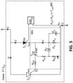
- the first mode of operation in which the current I is lower than the blocking current of a thyristor with higher rated current (T H1 ) ( I ⁇ I lH 1 ) and greater than the blocking current of the thyristor with lower rated current T L1 ( I ⁇ I iL 1 ), is illustrated in Figure 5 . Note that, for the proper operation of the static switch object of the invention, the minimum expected current must be greater than the blocking current of the thyristor with lower rated current (T L1 ) ( I min > I lL 1 ).
- the thyristor with lower rated current (T L1 ) must be selected so that it can conduct no-load current of the transformer, l 0 , which is the minimum possible current, so that I 0 > I lL 1 .
- the current would circulate through the thyristor with lower rated current (T L1 ). Note that the current would be circulating through the set formed by the capacitor (C 1 ) and the resistor (R c1 ), which would be subjected to a tension U C1 as shown in Figure 5 .
- the values of the capacitor (C 1 ) and the resistor (R c1 ) are adjusted such that the voltage U C 1 is lower than the avalanche voltage of the zener diode (D z1 ) so that it does not conduct at currents lower than I lH 1 . Therefore, the reduced current is conducted through the thyristor with lower rated current (T L1 ) and the triggering of the thyristor with higher rated current (T H1 ), due to the fact that the auxiliary thyristor (T aux1 ) is not triggered.
- the current is greater than or equal to the blocking current of the thyristor with the higher rated current (T H1 ) ( I ⁇ I lH 1 ), being able to ensure its proper conduction.
- T H1 the blocking current of the thyristor with the higher rated current (T H1 ) ( I ⁇ I lH 1 ), being able to ensure its proper conduction.
- a voltage is generated in the capacitor (C 1 ) such that the action of the zener diode (D z1 ) that causes current to flow through the gate of the auxiliary thyristor (T aux1 ) is produced, as shown in Figure 6A .
- the resistors (R a1 and R b1 ) form a current divider, so that in order to maximise the current to the gate of the auxiliary thyristor (T aux1 ), resistors must be selected fulfilling that R a1 /R b1 ⁇ 1.
- the triggering of the auxiliary thyristor (T aux1 ) will be produced if the voltage and current, U Gaux and I Gaux , at the gate of the auxiliary thyristor (T aux1 ) and shown in Figure 6A , are higher than the gate voltages and gate current of (T aux1 ) that guarantee the triggering thereof.
- the circuit shown in Figure 6B would result. So, the auxiliary thyristor (T aux1 ) feeds the gate of the thyristor with higher rated current (T H1 ), so that it will be triggered as long as the conditions for it are met.
- T H1 the thyristor with higher rated current
- U GT H1 and I GT H1 are greater than the corresponding voltage and current values of gate triggering for said thyristor.
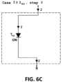
- the triggering of the thyristor with higher rated current (T H1 ) will be produced, so that the current would be exclusively conducted by this thyristor, as shown in Figure 6C .
Landscapes
- Engineering & Computer Science (AREA)
- Power Engineering (AREA)
- Power Conversion In General (AREA)
- Control Of Electrical Variables (AREA)
- Electronic Switches (AREA)
Abstract
Description
- It concerns a static AC switch with extended current range, for a static on-load tap changer in power transformers, based on the parallelisation of thyristors, which enables current to be conducted safely and autonomously over a wide range, from no-load to short-circuit currents, with respect to that of a single thyristor.
- Transformers, located in transformation centres, are massively used in electrical power distribution networks to reduce voltage levels from medium (usually 20 kV) to low (usually 400 V). These transformers are equipped with a fixed tap changer that allows the voltage on the low voltage side to be regulated, although it cannot be operated on load. Practically, the tap is adjusted at the time of installation of the transformer and is left in said position permanently for the entire useful life thereof.
- However, the transformation of said distribution networks towards future smart networks in which a massive presence of distributed generation and new agents, such as the electric car, is expected, makes it necessary to dynamically improve low-side voltage regulation, in order to which on-load tap-changers are required.
- On-load tap changers are widely used for large power transformers used in high voltage networks, although they are not conventional for distribution transformers. These are electromechanical devices characterised by being complex, bulky, with a limited number of manoeuvres and slow actuation times. For this reason, this conventional solution cannot be applied to distribution power transformers.
- In response to this need, tap changer technologies have been developed that are specially adapted to the characteristics of distribution transformers, among which those corresponding to the use of no-load switches and power electronic devices stand out.
- By way of example, within the first group patent documents of interest such as
WO2013156268A1 andEP3288053A1 can be found. From the second, documentES2734601B2 figure 1 . The topology combines a series of static switches (61a, 62a, 63a, 61b, 62b and 63b) especially suited for the configuration of windings (main 30a, 30b andregulation - The use of thyristors (like the one in
figure 2A ) with anti-parallel configuration, like the ones shown infigure 2B , is a known technical solution that is suited to the application due to the low losses thereof. This configuration is formed by two identical thyristors (T1 and T2) that are connected in anti-parallel to allow the bidirectional current flow required in AC applications. - However, there is no anti-parallel thyristor configuration on the market that is fully compatible with the technical requirements of the on-load tap-changer application for distribution transformers:
- i) High blocking voltages, since the tap changer is connected to the medium voltage side of the transformer where the regulating windings are usually located.
- ii) High short-time current, to be able to withstand possible short-circuit currents.
- iii) Reduced blocking currents (latching), to be able to operate reliably at low load or even with no-load.
- This last aspect is of vital importance today because, with the current European guidelines on the efficient design of transformers (in particular (EU) Regulation No 548/2014 of the Commission of 21 May 2014, which develops Directive 2009/125/EC of the European Parliament and of the Council with regard to small, medium and large power transformers), no-load currents are increasingly reduced.
- The object of the present invention is a static AC switch with extended current range, based on the association of thyristors which:
- i) Allows the bidirectional circulation of currents required for AC applications. For this, the association of thyristors of the proposed switch topology comprises a first set of thyristors (TH1 and TL1) connected in parallel and a corresponding second set of thyristors (TH2 and TL2) connected in parallel with identical characteristics, connected in anti-parallel to the first set of thyristors (TH1 and TL1).
- ii) Allows the circulation of a wide range of currents. To do this, two thyristors (TH1 and TL1), and the corresponding anti-parallel ones in the second set of thyristors (TH2 and TL2), the thyristors of each set being of different rated currents (In ), such that the rated current of a first thyristor of each set of thyristors is greater than the rated current of a second thyristor of each set of thyristors (I nH1 > I nL1 and I nH2 > I nL2). Given this ratio between rated currents, the blocking currents (Il ) in each set of thyristors will fulfill that I lH1 > I lL1 and I lH2 > I lL2.
- The topology of the proposed switch is applicable in those cases in which the minimum current to conduct, Imin , is lower than the blocking current of the thyristors with higher rated current of each set of thyristors (TH1 and TH2), that is I lH1,I lH2 > Imin. In particular, note that at currents I < I lH1, I lH2, there would be no effective conduction of the thyristors with higher rated current (TH1 and TH2) of each set of thyristors.
- The proposed topology, therefore, has the following operating principle:
- i) when the circulating current is very low, this is I < I lH1, I lH2, conduction is ensured by the thyristors with lower rated current (TL1 and TL2) of each set of thyristors, provided that the following is met I > I lH1, I lH2,
- ii) when the current is above a threshold, which is I > I lH1, I lH2, conduction is carried out exclusively by the thyristors with higher rated current (TH1 and TH2) of each set of thyristors.
- In this sense, the selection of the thyristors is of vital importance to achieve an operation such as that described in the previous points. Particularly, in the case of static on-load tap-changers for distribution transformers, the lowest current to be conducted corresponds to the no-load current of the transformer, I 0, so that the switches with lower rated current (TL1 and TL2) of each set of selected thyristors must verify that I 0 < I lH1, I lH2.
- In particular, the topology of the static AC switch object of the invention comprises:
- i) two terminals (A and B), intended to be connected to any external AC circuit in which it is required to control the current,
- ii) a first thyristor with lower rated current (TL1), and the corresponding anti-parallel thyristor (TL2) thereof of identical characteristics, each of the thyristors with lower rated current comprising an anode, a cathode and a gate,
- iii) two conventional trigger circuits (CDC1 and CDC2) connected to the thyristors with lower rated current (TL1 and TL2) through the gates thereof. The conventional trigger circuit can be based on any of the techniques commonly used for thyristors (pulse transformers, opto-coupling or using the anode voltage),
- iv) a control device connected to the conventional trigger circuit, which will operate the thyristors with lower rated current (TL1 and TL2),
- v) a first thyristor with higher rated current (TH1), and the corresponding anti-parallel thyristor with higher rated current (TH2), with identical characteristics, each of the thyristors with a higher rated current (TH1 and TH2) comprising an anode, a cathode and a gate,
- vi) two tri-terminal trigger circuits (DC1 and CD2), connected to the gates of the thyristors with higher rated current (TH1 and TH2), and which are specifically intended to achieve the performance described above.
- The proposed invention has advantages in relation to the current state of the art, since it achieves the formation of a static switch from a set of thyristors with different characteristics, which extends the operating range with respect to that of the individual thyristors that make it up, based on an asymmetrical distribution of the current through the thyristors that are parallelised.
- Thus, the static switch can be directly applied to static on-load tap changers for distribution transformers with reliable and safe switching with currents in a very wide range, which covers from no-load to short-circuit. Therefore, this invention solves the problem of the current static tap changers for power transformers, which can present operating problems in reduced current ranges (in the environment of the no-load current).
- The invention can be applied to medium/low voltage distribution transformers used in the following fields:
- Electric power distribution networks. Transformers belonging to electric companies that are required to supply customers connected at low voltage levels.
- Private customers with their own transformer that are directly connected at medium voltage.
- Photovoltaic inverter transformers coupled at medium voltage.
- Wind turbines.
- inverter transformers that are connected to power storage devices.
- To complement the description that is being made and for the purpose of helping to better understand the features of the invention according to a preferred practical exemplary embodiment thereof, a set of drawings is attached as an integral part of said description in which the following is depicted in an illustrative and non-limiting manner:
-
Figure 1 .- shows a topology of a tap changer for power transformers of the state of the art. -
Figure 2 .- shows static switches of the state of the art: (a) thyristor-based direct current (DC); (b) anti-parallel thyristor-based alternating current (AC). -
Figure 3 .- shows a topology with two thyristors with different rated current and tri-terminal trigger circuit proposed that operates on the thyristor with higher rated current: (a) static DC switch; (b) static AC switch. -
Figure 4 .- shows a possible tri-terminal trigger circuit that operates following the operating principle proposed. -
Figure 5 .- Current circulation in the case of I < I H1-L . -
Figure 6A .- Current circulation in the case of I ≥ I H1-L ,step 1. -
Figure 6B .- Current circulation in the case of I ≥ I H1-L ,step 2. -
Figure 6C .- Current circulation in the case of I ≥ I H1-L ,step 3. - With the help of
Figures 1 to 6C , a preferred embodiment of the AC static switch with extended current range, object of the present invention, is described below being of possible use for a static on-load tap changer of power transformer as shown inFigure 1 . However, its application is not limited to this case, the use thereof being able to be extended to any other alternative topology. - The highest voltage winding of the transformer, as shown in
Figure 1 , comprises a main winding (coils coils - In the case of multi-phase applications, there is an additional central control (100) that supervises the operation of each phase and sends the appropriate instructions to the local controllers. The actuation (on or off) of the static switches (61a, 62a, 63a and 61b, 62b, 63b) establishes the active regulating coils at each moment, so that the transformation ratio of the transformer and therefore, the secondary voltage, is dynamically controlled.
- Each of the static switches (61a, 62a, 63a and 61b, 62b, 63b) shown in
Figure 1 can be configured as shown inFigure 2B with two anti-parallel connected thyristors (T1, T2) having capacity for bidirectional current driving. However, as has been shown in the background of the invention, for the blocking voltages that are required in the application, there are no thyristors that cover the entire current range associated with the operation of the transformers (no-load current to short circuit current). - The present invention proposes a static switch topology wherein a first set of thyristors are parallelised, (TH1 and TL1), and the corresponding second set of anti-parallel thyristors, (TH2 and TL2) thereof, with identical characteristics and which verify that their rated currents are such that I nH1 > I nL1 and I nH2 > I nL2. Each of the sets of thyristors comprises a thyristor with higher rated current (TH1 and TH2), and a thyristor with lower rated current (TL1 and TL2), respectively.
- This parallelisation, shown in
Figure 3A for the DC version from which the AC version ofFigure 3B is formed, achieves the conduction of currents below the blocking current of the thyristors with higher rated current (TH1 and TH2), through the thyristors with lower rated current (TL1 and TL2), for which it is crucial to carry out an adequate design of tri-terminal trigger circuits (CD1 and CD2) linked to the thyristors. The interconnection of all these components that represents a preferred embodiment of the invention is shown inFigure 3B . - In particular, as shown in
Figure 3B , the static switch comprises: - i) A first thyristor with lower rated current (TL1), and the corresponding second thyristor with lower rated current (TL2) thereof connected in anti-parallel and with identical characteristics, the thyristors comprising an anode, a cathode and a gate.
- ii) A first and a second conventional trigger circuits (CDC1 and CDC2) of the thyristors with lower rated current (TL1 and TL2), the conventional trigger circuits (CDC1 and CDC2) being connected to the thyristors with lower rated current (TL1 and TL2) through the corresponding gates thereof.
- iii) A control device (CL) connected to the conventional trigger circuits (CDC1 and CDC2), the objective of which is to define the status (on or off) of the thyristors with lower rated current (TL1 and TL2), and therefore of the static AC switch object of the invention.
- iv) A first thyristor with higher rated current (TH1), and a second thyristor with higher rated current (TH2) connected in anti-parallel, with identical characteristics, the thyristors comprising an anode, a cathode and a gate.
- v) A first and a second tri-terminal trigger circuits (CD1 and CD2), respectively connected to the gates of the thyristors with higher rated current (TH1 and TH2).
- As shown in
Figure 3B , the anodes of the thyristors of the first set of thyristors (TH1 and TL1) are connected to the same first terminal (A), which is a first connection terminal of the static switch object of the invention. The anodes of the thyristors of the second set of thyristors (TH2 and TL2) are connected to the same second terminal (B) and form the second connection terminal of the static switch object of the invention. - Tri-terminal trigger circuits (CD1 and CD2) are connected to the following points respectively: first terminals (ta1 and ta2) to the cathodes of the thyristors with lower rated current (TL1 and TL2) respectively; second terminals (tb1 and tb2) to the cathodes of the thyristors with higher rated current (TH1 and TH2) respectively; finally third terminals (tc1 and tc2) to the gates of the thyristors with higher rated current (TH1 and TH2) respectively.
- Conventional trigger circuits (CDC1 and CDC2) are connected to the gate of the thyristors with lower rated current (TL1 and TL2) and the second terminals (tb1 and tb2) of the tri-terminal trigger circuits (CD1 and CD2) respectively.
- For its part,
Figure 4 shows a preferred embodiment of the tri-terminal trigger circuits (CD1 and CD2). The first tri-terminal trigger circuit (CD1) comprises the following components, the second tri-terminal trigger circuit (CD2) being identical: - i) a capacitor (C1), connected between the first terminal (ta1) and the second terminal (tb1).
- ii) a resistor (Rc1), connected between the first terminal (ta1) and the second terminal (tb1) and in parallel with the capacitor (C1).
- iii) an auxiliary thyristor (Taux1) connected between the first terminal (ta1) and the third terminal (tc1) with a series resistor (RgH1),
- iv) a voltage divider comprising resistors (Ra1 and Rb1) connected to the gate of the auxiliary thyristor (Taux1) and to the second terminal (tb1),
- v) a zener diode (Dz1), connected between the first terminal (ta1) and the midpoint of the voltage divider.
- This trigger circuit has the mission of causing the triggering of the thyristor with higher rated current, (TH1 or TH2), when the current circulating through the static switch is greater than the blocking current thereof, thus ensuring its proper conduction.
- The different modes of operation of the invention are explained in the case of a positive current conduction from the first terminal (A) to the second terminal (B) of the static switch, for which reason the thyristors of the first set (TH1, TL1) and the first tri-terminal trigger circuit (CD1) are involved in said explanation. The operation for the opposite direction of current circulation is identical, but with the anti-parallel components of the second set of thyristors (TH2, TL2) and the second tri-terminal trigger circuit (CD2). The configuration of the tri-terminal trigger circuits, (CD1 and CD2), allow operation according to the following operating principle depending on the current circulating through the static switch:
- i) Current lower than the blocking current of the thyristor with higher rated current (TH1) (I < I lH1), which is shown in
Figure 5 . Said current would be conducted through the thyristor with lower rated current (TL1) entering the tri-terminal trigger circuit (CD1) through the first terminal (ta1). The configuration of the trigger circuit is such that the outgoing current through the third terminal (tc1) is zero to prevent the triggering of the thyristor with higher rated current (TH1) that could not maintain its conduction because the circulating current was lower than the blocking current thereof. Therefore, the outgoing current through the second terminal (tb1) is identical to the incoming current through the first terminal (ta1), conduction being ensured by the switch with lower rated current (TL1). - ii) Current equal to or greater than the blocking current of the thyristor with higher rated current TH1 (I ≥ I lH1), as shown in
Figures 6A to 6C . As in the previous case, the current would begin to flow through the thyristor with lower rated current (TL1), entering the trigger circuit (CD1) by the first terminal (ta1). However, because the conditions are met for the thyristor with higher rated current (TH1) to have proper conduction, the triggering is carried out. For this, the design of the tri-terminal circuit (CD1) is such that it guarantees a certain outgoing current IGaux at the first terminal (tc1) (gate current of the thyristor with higher rated current (TH1)) and a voltage UGaux between the third terminal (tc1) and the second terminal (tb1) (gate-cathode voltage of the thyristor with higher rated current (TH1)) that cause the triggering of said thyristor. In this case, and until the triggering of the first thyristor with higher rated current (TH1) is produced, the outgoing current of the first terminal (tb1) will be the difference between the incoming current through the first terminal (ta1) and the outgoing current through the third terminal (tc1). From the moment in which the thyristor with higher rated current (TH1) begins to conduct, the current through the thyristor with lower rated current (TL1) is cancelled. - The first mode of operation, in which the current I is lower than the blocking current of a thyristor with higher rated current (TH1) (I < I lH1) and greater than the blocking current of the thyristor with lower rated current TL1 (I < I iL1), is illustrated in
Figure 5 . Note that, for the proper operation of the static switch object of the invention, the minimum expected current must be greater than the blocking current of the thyristor with lower rated current (TL1) (Imin > I lL1). In the case of using the static switch for static changers of power transformers, therefore, the thyristor with lower rated current (TL1) must be selected so that it can conduct no-load current of the transformer, l0 , which is the minimum possible current, so that I0 > I lL1. In this case, the current would circulate through the thyristor with lower rated current (TL1). Note that the current would be circulating through the set formed by the capacitor (C1) and the resistor (Rc1), which would be subjected to a tension UC1 as shown inFigure 5 . The values of the capacitor (C1) and the resistor (Rc1) are adjusted such that the voltage U C1 is lower than the avalanche voltage of the zener diode (Dz1) so that it does not conduct at currents lower than I lH1 . Therefore, the reduced current is conducted through the thyristor with lower rated current (TL1) and the triggering of the thyristor with higher rated current (TH1), due to the fact that the auxiliary thyristor (Taux1) is not triggered. - In the second operating mode, the current is greater than or equal to the blocking current of the thyristor with the higher rated current (TH1) (I ≥ I lH1), being able to ensure its proper conduction. The triggering process of said thyristor (TH1) follows the steps below.
- First, given the current I circulating, a voltage is generated in the capacitor (C1) such that the action of the zener diode (Dz1) that causes current to flow through the gate of the auxiliary thyristor (Taux1) is produced, as shown in
Figure 6A . Note that the resistors (Ra1 and Rb1) form a current divider, so that in order to maximise the current to the gate of the auxiliary thyristor (Taux1), resistors must be selected fulfilling that Ra1/Rb1<<1. In particular, the triggering of the auxiliary thyristor (Taux1) will be produced if the voltage and current, UGaux and IGaux , at the gate of the auxiliary thyristor (Taux1) and shown inFigure 6A , are higher than the gate voltages and gate current of (Taux1) that guarantee the triggering thereof. - As a consequence of the triggering of the auxiliary thyristor (Taux1) the circuit shown in
Figure 6B would result. So, the auxiliary thyristor (Taux1) feeds the gate of the thyristor with higher rated current (TH1), so that it will be triggered as long as the conditions for it are met. In particular, in the same way as in the case of the auxiliary thyristor (Taux1), it must be verified that U GTH1 and I GTH1 are greater than the corresponding voltage and current values of gate triggering for said thyristor. In this case, the triggering of the thyristor with higher rated current (TH1) will be produced, so that the current would be exclusively conducted by this thyristor, as shown inFigure 6C .
Claims (2)
- A static AC switch with extended current range, comprising:i) a first terminal (A) and a second terminal (B), intended to be connected to any external AC circuit in which current control is required,iii) a first set of two thyristors (TL1 and TH1) such that the rated currents thereof follow I nH1 > I nL1, which are connected in parallel to each other, each comprising an anode, a cathode and a gate, the anodes being connected to the first terminal (A),iii) a second set of two thyristors (TL2 and TH2) such that the rated currents thereof follow I nH2 > I nL2, which are connected in parallel to each other and anti-parallel with respect to the first set of thyristors (TL1 and TH1), each comprising an anode, a cathode and a gate, and the anodes being connected to the second terminal (B),iv) conventional trigger circuits (CDC1 and CDC2) connected to the gates and cathodes of the thyristors with lower rated current (TL1 and TL2) respectively, to generate the triggering of the same,v) a control device (CL) connected to the conventional trigger circuits (CDC1 and CDC2),vi) tri-terminal trigger circuits (CD1 and CD2) that manage the triggering of the thyristors with higher rated current, (TH1 and TH2), and comprising, respectively:i) first terminals (ta1 and ta2) connected to the cathodes of the thyristors with lower rated current (TL1 and TL2) respectively,ii) second terminals (tb1 and tb2) connected to the cathodes of the thyristors with higher rated current (TH1 and TH2), respectively, andiii) third terminals (tc1 and tc2) connected to the gate of the thyristors with higher rated current (TH1 and TH2).
- The static switch of claim 1, wherein each of the tri-terminal trigger circuits (CD1 and CD2) comprises:i) a capacitor (C1), connected between the first terminal (ta1) and the second terminal (tb1),ii) a resistor (Rc1), connected between the first terminal (ta1) and the second terminal (tb1) and in parallel with the capacitor (C1),iii) an auxiliary thyristor (Taux1) connected between the first terminal (ta1) and the third terminal (tc1) with a series resistor (RgH1),iv) a voltage divider comprising resistors (Ra1 and Rb1), connected to the gate of the auxiliary thyristor (Taux1) and to the second terminal (tb1),v) a zener diode (Dz1), connected between the first terminal (ta1) and a midpoint of the voltage divider.
Applications Claiming Priority (2)
| Application Number | Priority Date | Filing Date | Title |
|---|---|---|---|
| ES202130853A ES2936183B2 (en) | 2021-09-14 | 2021-09-14 | STATIC AC CURRENT SWITCH WITH EXTENDED CURRENT RANGE |
| PCT/ES2022/070569 WO2023041825A1 (en) | 2021-09-14 | 2022-09-12 | Static ac switch with extended current range |
Publications (2)
| Publication Number | Publication Date |
|---|---|
| EP4404463A1 true EP4404463A1 (en) | 2024-07-24 |
| EP4404463B1 EP4404463B1 (en) | 2026-03-18 |
Family
ID=84245782
Family Applications (1)
| Application Number | Title | Priority Date | Filing Date |
|---|---|---|---|
| EP22800308.3A Active EP4404463B1 (en) | 2021-09-14 | 2022-09-12 | Static ac switch with extended current range |
Country Status (3)
| Country | Link |
|---|---|
| EP (1) | EP4404463B1 (en) |
| ES (1) | ES2936183B2 (en) |
| WO (1) | WO2023041825A1 (en) |
Cited By (1)
| Publication number | Priority date | Publication date | Assignee | Title |
|---|---|---|---|---|
| EP4482033A1 (en) * | 2023-06-20 | 2024-12-25 | Schneider Electric IT Corporation | Systems and methods of operating thyristors coupled in parallel |
Families Citing this family (1)
| Publication number | Priority date | Publication date | Assignee | Title |
|---|---|---|---|---|
| FR3159061A1 (en) * | 2024-02-07 | 2025-08-08 | Stmicroelectronics International N.V. | Load switching device |
Family Cites Families (7)
| Publication number | Priority date | Publication date | Assignee | Title |
|---|---|---|---|---|
| US5619081A (en) * | 1994-01-18 | 1997-04-08 | Leviton Manufacturing Co., Inc. | Asymmetrical AC trigger simulation |
| FR2810471B1 (en) * | 2000-06-16 | 2002-11-29 | St Microelectronics Sa | BISTABLE BIDIRECTIONAL SWITCH |
| DE202012101475U1 (en) | 2012-04-20 | 2013-07-23 | Maschinenfabrik Reinhausen Gmbh | OLTC |
| CN103781258B (en) * | 2014-02-24 | 2015-09-30 | 彭云 | Light adjusting circuit and use the illumination control apparatus of this light adjusting circuit |
| ES2709770T3 (en) | 2015-04-21 | 2019-04-17 | Ormazabal Corporate Tech A I E | On-load tap changer device |
| EP3316070B1 (en) * | 2016-10-27 | 2022-06-15 | Hitachi Energy Switzerland AG | Power electronic tap changer module for transformer |
| ES2734601B2 (en) | 2018-06-06 | 2020-07-08 | Univ Sevilla | STATIC CHANGING DEVICE FOR CHARGING INPUTS FOR TRANSFORMERS WITH DISCONTINUOUS REGULATION WINDINGS |
-
2021
- 2021-09-14 ES ES202130853A patent/ES2936183B2/en active Active
-
2022
- 2022-09-12 WO PCT/ES2022/070569 patent/WO2023041825A1/en not_active Ceased
- 2022-09-12 EP EP22800308.3A patent/EP4404463B1/en active Active
Cited By (1)
| Publication number | Priority date | Publication date | Assignee | Title |
|---|---|---|---|---|
| EP4482033A1 (en) * | 2023-06-20 | 2024-12-25 | Schneider Electric IT Corporation | Systems and methods of operating thyristors coupled in parallel |
Also Published As
| Publication number | Publication date |
|---|---|
| ES2936183B2 (en) | 2023-12-27 |
| ES2936183A1 (en) | 2023-03-14 |
| WO2023041825A1 (en) | 2023-03-23 |
| EP4404463B1 (en) | 2026-03-18 |
Similar Documents
| Publication | Publication Date | Title |
|---|---|---|
| US9748848B2 (en) | Modular multilevel DC/DC converter for HVDC applications | |
| US9041251B2 (en) | Boost converter with multiple inputs and inverter circuit | |
| US20080079314A1 (en) | System for bypassing a power cell of a power supply | |
| EP3696961B1 (en) | Power conversion device | |
| CN111697847B (en) | Weissach rectifier components | |
| EP4404463B1 (en) | Static ac switch with extended current range | |
| Li et al. | A hybrid modular multilevel converter with reduced full-bridge submodules | |
| MX2024001145A (en) | Systems and methods for control of zero-sequence stabilized power converters. | |
| US10680428B2 (en) | Energy supply | |
| US9882371B2 (en) | Direct current voltage switch for switching a direct current in a branch of a direct current voltage network node | |
| US11777401B2 (en) | Fault tolerant AC-DC chain-link converter | |
| US20120113694A1 (en) | Step-down converter and inverter circuit | |
| Heinig et al. | Implications of capacitor voltage imbalance on the operation of the semi-full-bridge submodule | |
| US20230104735A1 (en) | Fuel Cell Power System | |
| Feretti et al. | Family of non-isolated high step-up DC–DC converters based on the multi-state switching cell | |
| EP2996215A1 (en) | A voltage source converter | |
| US20110188277A1 (en) | Circuit configuration with a step-up converter, and inverter circuit having such a circuit configuration | |
| Dassanayake et al. | Self-Powered and Self-Controlled Hybrid DC Circuit Breaker for Low Voltage Applications | |
| Wambsganss | Regulating transformer rectifier unit (R-TRU) for more electric aircraft (MEA) | |
| Lokhande et al. | Design and implementation of triac based on load tap changer with primary tappings for constant output voltage | |
| EP2274826B1 (en) | An arrangement for voltage conversion | |
| CN114128074A (en) | Method for generating inductive reactive power by means of an electrical load device, electrical load device and electrolysis device | |
| US10320308B2 (en) | Commutating circuit | |
| KR102409038B1 (en) | Modular Power Quality Compensation Device for Electrified Railway Network with Enhanced Bypass Capability | |
| US11671048B2 (en) | Multiphase voltage transformer for a supply network and method for powering down an intermediate circuit voltage of this supply network |
Legal Events
| Date | Code | Title | Description |
|---|---|---|---|
| STAA | Information on the status of an ep patent application or granted ep patent |
Free format text: STATUS: UNKNOWN |
|
| STAA | Information on the status of an ep patent application or granted ep patent |
Free format text: STATUS: THE INTERNATIONAL PUBLICATION HAS BEEN MADE |
|
| PUAI | Public reference made under article 153(3) epc to a published international application that has entered the european phase |
Free format text: ORIGINAL CODE: 0009012 |
|
| STAA | Information on the status of an ep patent application or granted ep patent |
Free format text: STATUS: REQUEST FOR EXAMINATION WAS MADE |
|
| 17P | Request for examination filed |
Effective date: 20240318 |
|
| AK | Designated contracting states |
Kind code of ref document: A1 Designated state(s): AL AT BE BG CH CY CZ DE DK EE ES FI FR GB GR HR HU IE IS IT LI LT LU LV MC MK MT NL NO PL PT RO RS SE SI SK SM TR |
|
| DAV | Request for validation of the european patent (deleted) | ||
| DAX | Request for extension of the european patent (deleted) | ||
| GRAP | Despatch of communication of intention to grant a patent |
Free format text: ORIGINAL CODE: EPIDOSNIGR1 |
|
| STAA | Information on the status of an ep patent application or granted ep patent |
Free format text: STATUS: GRANT OF PATENT IS INTENDED |
|
| INTG | Intention to grant announced |
Effective date: 20251015 |
|
| GRAS | Grant fee paid |
Free format text: ORIGINAL CODE: EPIDOSNIGR3 |
|
| GRAA | (expected) grant |
Free format text: ORIGINAL CODE: 0009210 |
|
| STAA | Information on the status of an ep patent application or granted ep patent |
Free format text: STATUS: THE PATENT HAS BEEN GRANTED |
|
| AK | Designated contracting states |
Kind code of ref document: B1 Designated state(s): AL AT BE BG CH CY CZ DE DK EE ES FI FR GB GR HR HU IE IS IT LI LT LU LV MC MK MT NL NO PL PT RO RS SE SI SK SM TR |
|
| REG | Reference to a national code |
Ref country code: CH Ref legal event code: F10 Free format text: ST27 STATUS EVENT CODE: U-0-0-F10-F00 (AS PROVIDED BY THE NATIONAL OFFICE) Effective date: 20260318 Ref country code: GB Ref legal event code: FG4D |
|
| REG | Reference to a national code |
Ref country code: IE Ref legal event code: FG4D |
|
| REG | Reference to a national code |
Ref country code: DE Ref legal event code: R096 Ref document number: 602022032653 Country of ref document: DE |