EP4404373A1 - Circuit board - Google Patents
Circuit board Download PDFInfo
- Publication number
- EP4404373A1 EP4404373A1 EP22869917.9A EP22869917A EP4404373A1 EP 4404373 A1 EP4404373 A1 EP 4404373A1 EP 22869917 A EP22869917 A EP 22869917A EP 4404373 A1 EP4404373 A1 EP 4404373A1
- Authority
- EP
- European Patent Office
- Prior art keywords
- dielectric
- circuit board
- conductor
- dielectric layer
- permittivity
- Prior art date
- Legal status (The legal status is an assumption and is not a legal conclusion. Google has not performed a legal analysis and makes no representation as to the accuracy of the status listed.)
- Pending
Links
Images


Classifications
-
- H—ELECTRICITY
- H05—ELECTRIC TECHNIQUES NOT OTHERWISE PROVIDED FOR
- H05K—PRINTED CIRCUITS; CASINGS OR CONSTRUCTIONAL DETAILS OF ELECTRIC APPARATUS; MANUFACTURE OF ASSEMBLAGES OF ELECTRICAL COMPONENTS
- H05K3/00—Apparatus or processes for manufacturing printed circuits
- H05K3/46—Manufacturing multilayer circuits
-
- H—ELECTRICITY
- H05—ELECTRIC TECHNIQUES NOT OTHERWISE PROVIDED FOR
- H05K—PRINTED CIRCUITS; CASINGS OR CONSTRUCTIONAL DETAILS OF ELECTRIC APPARATUS; MANUFACTURE OF ASSEMBLAGES OF ELECTRICAL COMPONENTS
- H05K1/00—Printed circuits
- H05K1/02—Details
- H05K1/0213—Electrical arrangements not otherwise provided for
- H05K1/0237—High frequency adaptations
- H05K1/024—Dielectric details, e.g. changing the dielectric material around a transmission line
-
- H—ELECTRICITY
- H01—ELECTRIC ELEMENTS
- H01P—WAVEGUIDES; RESONATORS, LINES, OR OTHER DEVICES OF THE WAVEGUIDE TYPE
- H01P3/00—Waveguides; Transmission lines of the waveguide type
- H01P3/02—Waveguides; Transmission lines of the waveguide type with two longitudinal conductors
- H01P3/08—Microstrips; Strip lines
-
- H—ELECTRICITY
- H01—ELECTRIC ELEMENTS
- H01P—WAVEGUIDES; RESONATORS, LINES, OR OTHER DEVICES OF THE WAVEGUIDE TYPE
- H01P3/00—Waveguides; Transmission lines of the waveguide type
- H01P3/02—Waveguides; Transmission lines of the waveguide type with two longitudinal conductors
- H01P3/08—Microstrips; Strip lines
- H01P3/081—Microstriplines
- H01P3/082—Multilayer dielectric
-
- H—ELECTRICITY
- H01—ELECTRIC ELEMENTS
- H01P—WAVEGUIDES; RESONATORS, LINES, OR OTHER DEVICES OF THE WAVEGUIDE TYPE
- H01P3/00—Waveguides; Transmission lines of the waveguide type
- H01P3/02—Waveguides; Transmission lines of the waveguide type with two longitudinal conductors
- H01P3/08—Microstrips; Strip lines
- H01P3/085—Triplate lines
-
- H—ELECTRICITY
- H05—ELECTRIC TECHNIQUES NOT OTHERWISE PROVIDED FOR
- H05K—PRINTED CIRCUITS; CASINGS OR CONSTRUCTIONAL DETAILS OF ELECTRIC APPARATUS; MANUFACTURE OF ASSEMBLAGES OF ELECTRICAL COMPONENTS
- H05K1/00—Printed circuits
- H05K1/02—Details
- H05K1/0213—Electrical arrangements not otherwise provided for
- H05K1/0216—Reduction of cross-talk, noise or electromagnetic interference
- H05K1/0218—Reduction of cross-talk, noise or electromagnetic interference by printed shielding conductors, ground planes or power plane
- H05K1/0224—Patterned shielding planes, ground planes or power planes
- H05K1/0225—Single or multiple openings in a shielding, ground or power plane
-
- H—ELECTRICITY
- H05—ELECTRIC TECHNIQUES NOT OTHERWISE PROVIDED FOR
- H05K—PRINTED CIRCUITS; CASINGS OR CONSTRUCTIONAL DETAILS OF ELECTRIC APPARATUS; MANUFACTURE OF ASSEMBLAGES OF ELECTRICAL COMPONENTS
- H05K2201/00—Indexing scheme relating to printed circuits covered by H05K1/00
- H05K2201/01—Dielectrics
- H05K2201/0183—Dielectric layers
- H05K2201/0191—Dielectric layers wherein the thickness of the dielectric plays an important role
-
- H—ELECTRICITY
- H05—ELECTRIC TECHNIQUES NOT OTHERWISE PROVIDED FOR
- H05K—PRINTED CIRCUITS; CASINGS OR CONSTRUCTIONAL DETAILS OF ELECTRIC APPARATUS; MANUFACTURE OF ASSEMBLAGES OF ELECTRICAL COMPONENTS
- H05K2201/00—Indexing scheme relating to printed circuits covered by H05K1/00
- H05K2201/01—Dielectrics
- H05K2201/0183—Dielectric layers
- H05K2201/0195—Dielectric or adhesive layers comprising a plurality of layers, e.g. in a multilayer structure
Definitions
- the present invention relates to a circuit board.
- an apparatus such as a smartphone or a millimeter-wave radar, transmits and receives radio waves and incorporates various components such as an antenna and a circuit board. Such components transmit and receive radio waves.
- a loss dielectric loss
- an antenna feeder line or the like is desirably reduced.
- Patent Literature 1 discloses that, in a circuit board, an air space is physically provided in an insulating layer between a metal conductor and a power supply layer so as to reduce an effective relative permittivity.
- Patent Literature 2 discloses that, in a circuit board, a hollow space is provided between a center conductor and an electrode so as to reduce an effective relative permittivity.
- Patent Literature 3 discloses the disposition of a dielectric material between a pair of differential wires in an inner layer of a printed circuit board. Dielectric layers sandwich, from above and below, a layer including the differential wires. The dielectric material has a permittivity lower than those of the dielectric layers.
- Patent Literature 4 discloses that loss reduction is achieved by using a low-loss dielectric, in a circuit board, in a signal layer sandwiched between insulating layers, for the thin insulating layer side to concentrate an electric field generated by a signal onto the low-loss dielectric side.
- a circuit board includes a first conductor, a second conductor, a transmission line, a first dielectric layer, and a second dielectric layer.
- the transmission line is disposed between the first conductor and the second conductor.
- the first dielectric layer is disposed between the first conductor and the transmission line.
- the first dielectric layer includes at least one first dielectric.
- the second dielectric layer is disposed between the second conductor and the transmission line.
- the second dielectric layer includes at least one second dielectric.
- the second dielectric layer is thicker than the first dielectric layer.
- the permittivity and/or the dielectric dissipation factor of the first dielectric is smaller than the permittivity and/or the dielectric dissipation factor of the second dielectric.
- a loss in an antenna feeder line of a circuit board is desirably reduced.
- the reduced manufacturing cost of such a circuit board has an advantage.
- the present disclosure provides a circuit board enabling loss reduction and, at the same time, suppression of the manufacturing cost.
- a circuit board enabling loss reduction and, at the same time, suppression of the manufacturing cost can be provided.
- FIG. 1 is a schematic view of the overall configuration of a circuit board according to an embodiment.
- the use of the circuit board is not particularly limited.
- the circuit board may be used for an apparatus that transmits and receives radio waves, such as a smartphone or a millimeter-wave radar.
- a circuit board 1 may be, for example, a hybrid multilayer board.
- FIG. 1 illustrates a cross section of the circuit board 1 according to an embodiment.
- the circuit board 1 illustrated in FIG. 1 has a structure multilayered in the Z-axis direction given in the figure. That is, the thickness direction of the circuit board 1 illustrated in FIG. 1 may be the Z-axis direction given in the figure.
- a signal line strip line
- the circuit board 1 illustrated in FIG. 1 may transmit a signal in the Y-axis direction given in the figure.
- the circuit board 1 includes conductors 11 to 18.
- Each of the conductors 11 to 18 may contain, for example, copper.
- FIG. 1 illustrates an example of the circuit board 1, according to an embodiment, having an eight-layer structure of the conductors 11 to 18.
- the structure of the circuit board 1 is not limited to the eight-layer structure and may be a multilayer structure of any number of layers.
- the circuit board 1 includes dielectric layers 21 to 27.
- Each of the dielectric layers 21 to 27 may be disposed between corresponding conductors of the conductors 11 to 18.
- Each of the dielectric layers 21 to 27 may include any dielectric.
- each of the dielectric layers 21 to 27 may be formed by using, for example, an FR-4 standard resin material.
- the dielectric layer 21 and the dielectric layer 27 may be formed by using, for example, a base material having a relatively low permittivity and/or dielectric dissipation factor. That is, the permittivity and/or the dielectric dissipation factor of each of the dielectric layer 21 and the dielectric layer 27 may be lower than a predetermined value.
- the dielectric layer 21 and the dielectric layer 27 may be used for a millimeter wave band, for example.
- the dielectric loss of a transmission line can be expressed as ⁇ (transmission loss) in Equation (1) below.
- Equation (1) K represents a proportionality constant, f represents a frequency, ⁇ r represents a relative permittivity, and tan ⁇ represents a dielectric dissipation factor.
- K K ⁇ f ⁇ ⁇ ⁇ r ⁇ tan ⁇
- the dielectric loss of the transmission line which is represented by ⁇ in Equation (1) above, is proportional to both the permittivity and the dielectric dissipation factor.
- ⁇ in Equation (1) above is proportional to both the permittivity and the dielectric dissipation factor.
- at least one of the permittivity and the dielectric dissipation factor of each of the dielectric layer 21 and the dielectric layer 27 may be reduced.
- examples of the values of a low permittivity and a low dielectric dissipation factor include the following values.
- the permittivity Dk is 4.4 and the dielectric dissipation factor Df is 0.02 at 10 GHz in an FR-4 standard resin material, whereas the permittivity Dk may be 3.0 and the dielectric dissipation factor Df may be 0.001 at 10 GHz.
- the above values may vary depending on the material manufacturer, the model number, the frequency to be used, and/or the ambient temperature.
- the permittivity may be a relative permittivity.
- the dielectric dissipation factor (tan ⁇ ) is a numerical value representing the degree of the electric energy loss (energy loss rate) in a dielectric.
- the dielectric dissipation factor (tan ⁇ ) can be expressed by Equation (2) below, where Ic represents a signal current, and Ir represents a loss current.
- tan ⁇ Ir / Ic
- the conductor 14 and the conductor 15 of copper plates may be pressed with the dielectric layer 24 as a core material.
- the dielectric layers 22, 23, 25, and 26 may each be a prepreg, for example.
- FIG. 2 illustrates a comparative example for explaining the circuit board 1 according to an embodiment. That is, FIG. 2 illustrates a part of a circuit board 100 as a comparative example for comparison with the circuit board 1 according to an embodiment.
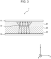
- FIG. 3 illustrates a part of the circuit board 1 according to an embodiment.
- a signal may be transmitted in the Y-axis direction given in the figures.
- each of both the circuit board 100 illustrated in FIG. 2 and the circuit board 1 illustrated in FIG. 3 includes a signal line in an inner layer of the board.
- the circuit board 100 illustrated in FIG. 2 includes a transmission line 12 between a conductor 11 and a conductor 13.
- the circuit board 100 illustrated in FIG. 2 further includes a dielectric layer 21 and a dielectric layer 22 between the conductor 11 and the conductor 13.
- the circuit board 1 illustrated in FIG. 3 includes a transmission line 12 between the conductor 11 and the conductor 14.
- the circuit board 1 illustrated in FIG. 3 further includes the dielectric layer 21, the dielectric layer 22, and the dielectric layer 23 between the conductor 11 and the conductor 14.
- each of both the circuit board 100 illustrated in FIG. 2 and the circuit board 1 illustrated in FIG. 3 includes a strip line.
- the strip line has a structure in which the transmission line 12 is sandwiched between the conductors and the dielectric layers in the up-down direction (the Z-axis direction).
- the transmission line 12 serves as the signal line.
- the distance between the conductor 11 and the transmission line 12 is larger than the distance between the transmission line 12 and the conductor 13. That is, in the circuit board 100 illustrated in FIG. 2 , the dielectric layer 21 has a relatively low permittivity and/or dielectric dissipation factor.
- the dielectric layer 21 has a thickness (the size in the Z-axis direction given in the figure) larger than the dielectric layer 22 of a prepreg.
- the permittivity and/or the dielectric dissipation factor of the dielectric layer 22 may be larger than the permittivity and/or the dielectric dissipation factor of the dielectric layer 21.
- the conductor 13 is omitted from the circuit board 1 illustrated in FIG. 3 as compared with the structure in FIG. 1 .
- the distance between the conductor 11 and the transmission line 12 is smaller than the distance between the transmission line 12 and the conductor 14.
- a large part of the electric field distribution of the signal line enters the conductor 11 closer to a ground plane as FIG. 3 illustrates. That is, in the electric field distribution of the signal line, the dielectric layer 21 having a small permittivity and/or dielectric dissipation factor is dominant.
- the circuit board 1 illustrated in FIG. 3 enables a reduction in the transmission loss of the transmission line 12.
- the circuit board 1 includes a first conductor 11, a second conductor 14, the transmission line 12, a first dielectric layer 21, and a second dielectric layer (22 and 23).
- the transmission line 12 may be disposed between the first conductor 11 and the second conductor 14.
- the first dielectric layer 21 is disposed between the first conductor 11 and the transmission line 12 and may include at least one first dielectric.
- the second dielectric layer (22 and 23) is disposed between the second conductor 14 and the transmission line 12 and may include at least one second dielectric.
- the second dielectric layer (22 and 23) is made thicker than the first dielectric layer 21.
- the permittivity and/or the dielectric dissipation factor of the first dielectric in the first dielectric layer 21 is smaller than the permittivity and/or the dielectric dissipation factor of the second dielectric in the second dielectric layer (22 and 23).
- the circuit board 1 enables a reduction in the transmission loss of the transmission line 12.
- the circuit board 1 also enables a reduction in the amount of the use of a dielectric having a low permittivity and/or dielectric dissipation factor, which is relatively expensive.
- the circuit board 1 can be provided as a circuit board enabling a reduction in loss while manufactured at a cost kept low.
- the dielectric layers layered in the up-down direction may be made of the same kind of material so as to more favorably direct electrolysis to a dielectric having a small permittivity and/or dielectric dissipation factor. That is, in the circuit board 1 according to an embodiment, the first dielectric of the first dielectric layer 21 and the second dielectric of the second dielectric layer (22 and 23) may be made of the same kind of material.
- the circuit board 1 illustrated in FIG. 3 has been described as compared with the structure in FIG. 1 .
- FIG. 3 an example in which the conductor 13 is completely omitted has been described.
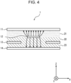
- the circuit board 1 may have a structure in which a part of the conductor 13 is omitted as compared with the structure in FIG. 1 .
- the signal line the transmission line 12
- the other parts of the conductor 13 existing in the regions other than the region immediately below (the negative direction of the Z axis given in the figure) the signal line (the transmission line 12) may serve as, for example, a ground plane.
- a part of the conductor 13 existing in a small region adjacent to the region immediately below the transmission line 12 (the negative direction of the Z axis given in the figure) may be further removed.
- Patent Literature 1 For example, as in Patent Literature 1 described above, reducing an effective permittivity by physically providing an air space in an insulating layer between a conductor and a power supply layer can be considered.
- the permittivity of air (or vacuum) is 1, and air can thus be an ideal insulating layer.
- a special manufacturing process is required to form an air space as in Patent Literature 1.
- Such a structure may increase the cost.
- the insulating layer has a very thin structure; thus, forming an air space with high accuracy may be difficult.
- the replacement of the upper and lower layers with a material having a low permittivity, particularly a low dielectric dissipation factor increases the material cost. Accordingly, the manufacturing cost of such a circuit board tends to increase.
- replacing only one side with a material having a low permittivity, particularly a low dielectric dissipation factor can be considered.
- Patent Literature 4 described above in a signal layer sandwiched between insulating layers (that is, a strip line is formed), a low-loss dielectric is used for the thin insulating layer side to concentrate an electric field generated by a signal onto the low-loss dielectric side.
- the printed wiring board disclosed in Patent Literature 4 described above loss reduction can be expected, and an increase in cost can be suppressed to some extent by using an expensive low-loss dielectric only for one side.
- the configuration using such a low-loss dielectric is adopted only when the thickness of the layer of the low permittivity material is made small.
- circuit board 1 With the circuit board 1 according to an embodiment, such problems, which are mentioned in the above description of the patent literatures, can be overcome.
- the permittivity and/or the dielectric dissipation factor of the dielectric between the signal line and the conductor positioned close to the signal line is made relatively small, and the permittivity and/or the dielectric dissipation factor can thereby be equivalently reduced.
- the loss can be kept low.
- a material having a low permittivity and/or dielectric dissipation factor may be a cause of cost increase.
- a material having a low permittivity and/or dielectric dissipation factor is mounted only on one side.
- the circuit board 1 enables suppression of an increase in material cost.
- the circuit board 1 of an embodiment even when a layer on the side where the permittivity and/or the dielectric dissipation factor is low is thick, the loss (dielectric loss) can be kept low only by changing a pattern without changing the thickness of the layer. That is, in an embodiment, the circuit board 1 can be manufactured through an existing process, without being subjected to a special manufacturing process. Thus, the circuit board 1 enables suppression of an increase in manufacturing cost.
Landscapes
- Engineering & Computer Science (AREA)
- Microelectronics & Electronic Packaging (AREA)
- Manufacturing & Machinery (AREA)
- Structure Of Printed Boards (AREA)
- Production Of Multi-Layered Print Wiring Board (AREA)
- Waveguides (AREA)
Abstract
Description
- This application claims priority to and the benefit of
Japanese Patent Application No. 2021-152596 filed on Sep. 17, 2021 - The present invention relates to a circuit board.
- For example, an apparatus, such as a smartphone or a millimeter-wave radar, transmits and receives radio waves and incorporates various components such as an antenna and a circuit board. Such components transmit and receive radio waves. In such an apparatus, for example, a loss (dielectric loss) in an antenna feeder line or the like is desirably reduced. Several proposals have been made to reduce the loss in the antenna feeder line or the like.
- For example,
Patent Literature 1 discloses that, in a circuit board, an air space is physically provided in an insulating layer between a metal conductor and a power supply layer so as to reduce an effective relative permittivity. Patent Literature 2 discloses that, in a circuit board, a hollow space is provided between a center conductor and an electrode so as to reduce an effective relative permittivity. Patent Literature 3 discloses the disposition of a dielectric material between a pair of differential wires in an inner layer of a printed circuit board. Dielectric layers sandwich, from above and below, a layer including the differential wires. The dielectric material has a permittivity lower than those of the dielectric layers. Patent Literature 4 discloses that loss reduction is achieved by using a low-loss dielectric, in a circuit board, in a signal layer sandwiched between insulating layers, for the thin insulating layer side to concentrate an electric field generated by a signal onto the low-loss dielectric side. -
- Patent Literature 1:
Japanese Unexamined Patent Application Publication No. 2008-160750 - Patent Literature 2:
Japanese Unexamined Patent Application Publication No. 2005-303778 - Patent Literature 3:
Japanese Unexamined Patent Application Publication No. 2009-141233 - Patent Literature 4:
Japanese Unexamined Patent Application Publication No. 2007-96159 - In an embodiment, a circuit board includes a first conductor, a second conductor, a transmission line, a first dielectric layer, and a second dielectric layer.
- The transmission line is disposed between the first conductor and the second conductor. The first dielectric layer is disposed between the first conductor and the transmission line. The first dielectric layer includes at least one first dielectric.
- The second dielectric layer is disposed between the second conductor and the transmission line. The second dielectric layer includes at least one second dielectric.
- The second dielectric layer is thicker than the first dielectric layer.
- The permittivity and/or the dielectric dissipation factor of the first dielectric is smaller than the permittivity and/or the dielectric dissipation factor of the second dielectric.
-
-
FIG. 1 illustrates a cross section, in a predetermined direction, of a circuit board according to an embodiment. -
FIG. 2 illustrates a cross section, in a predetermined direction, of a comparative example given for explaining the circuit board according to an embodiment. -
FIG. 3 illustrates a cross section, in a predetermined direction, of the circuit board according to an embodiment. -
FIG. 4 illustrates a cross section, in a predetermined direction, of the circuit board according to an embodiment. - A loss in an antenna feeder line of a circuit board is desirably reduced. The reduced manufacturing cost of such a circuit board has an advantage. The present disclosure provides a circuit board enabling loss reduction and, at the same time, suppression of the manufacturing cost. According to an embodiment, a circuit board enabling loss reduction and, at the same time, suppression of the manufacturing cost can be provided. Hereinafter, an embodiment will be detailed with reference to the drawings.
-
FIG. 1 is a schematic view of the overall configuration of a circuit board according to an embodiment. In an embodiment, the use of the circuit board is not particularly limited. For example, the circuit board may be used for an apparatus that transmits and receives radio waves, such as a smartphone or a millimeter-wave radar. - As
FIG. 1 illustrates, in an embodiment, acircuit board 1 may be, for example, a hybrid multilayer board.FIG. 1 illustrates a cross section of thecircuit board 1 according to an embodiment. Thecircuit board 1 illustrated inFIG. 1 has a structure multilayered in the Z-axis direction given in the figure. That is, the thickness direction of thecircuit board 1 illustrated inFIG. 1 may be the Z-axis direction given in the figure. As will be described later, in an embodiment, a signal line (strip line) may be configured in thecircuit board 1. Thecircuit board 1 illustrated inFIG. 1 may transmit a signal in the Y-axis direction given in the figure. - As
FIG. 1 illustrates, in an embodiment, thecircuit board 1 includesconductors 11 to 18. Each of theconductors 11 to 18 may contain, for example, copper.FIG. 1 illustrates an example of thecircuit board 1, according to an embodiment, having an eight-layer structure of theconductors 11 to 18. However, in an embodiment, the structure of thecircuit board 1 is not limited to the eight-layer structure and may be a multilayer structure of any number of layers. - As
FIG. 1 illustrates, in an embodiment, thecircuit board 1 includesdielectric layers 21 to 27. Each of thedielectric layers 21 to 27 may be disposed between corresponding conductors of theconductors 11 to 18. Each of thedielectric layers 21 to 27 may include any dielectric. In an embodiment, each of thedielectric layers 21 to 27 may be formed by using, for example, an FR-4 standard resin material. - Among the
dielectric layers 21 to 27 illustrated inFIG. 1 , thedielectric layer 21 and the dielectric layer 27 may be formed by using, for example, a base material having a relatively low permittivity and/or dielectric dissipation factor. That is, the permittivity and/or the dielectric dissipation factor of each of thedielectric layer 21 and the dielectric layer 27 may be lower than a predetermined value. Thedielectric layer 21 and the dielectric layer 27 may be used for a millimeter wave band, for example. In the present disclosure, the dielectric loss of a transmission line can be expressed as α (transmission loss) in Equation (1) below. In Equation (1), K represents a proportionality constant, f represents a frequency, εr represents a relative permittivity, and tanδ represents a dielectric dissipation factor.
- The dielectric loss of the transmission line, which is represented by α in Equation (1) above, is proportional to both the permittivity and the dielectric dissipation factor. Thus, in the
circuit board 1 according to an embodiment, at least one of the permittivity and the dielectric dissipation factor of each of thedielectric layer 21 and the dielectric layer 27 may be reduced. In an example of a material used for an existing millimeter-wave radar, examples of the values of a low permittivity and a low dielectric dissipation factor include the following values. That is, for example, the permittivity Dk is 4.4 and the dielectric dissipation factor Df is 0.02 at 10 GHz in an FR-4 standard resin material, whereas the permittivity Dk may be 3.0 and the dielectric dissipation factor Df may be 0.001 at 10 GHz. However, the above values may vary depending on the material manufacturer, the model number, the frequency to be used, and/or the ambient temperature. - In the present disclosure, the permittivity may be a relative permittivity. The dielectric dissipation factor (tanδ) is a numerical value representing the degree of the electric energy loss (energy loss rate) in a dielectric. The dielectric dissipation factor (tanδ) can be expressed by Equation (2) below, where Ic represents a signal current, and Ir represents a loss current.

- As
FIG. 1 illustrates, in thecircuit board 1 according to an embodiment, theconductor 14 and theconductor 15 of copper plates may be pressed with thedielectric layer 24 as a core material. The dielectric layers 22, 23, 25, and 26 may each be a prepreg, for example. -
FIG. 2 illustrates a comparative example for explaining thecircuit board 1 according to an embodiment. That is,FIG. 2 illustrates a part of acircuit board 100 as a comparative example for comparison with thecircuit board 1 according to an embodiment.FIG. 3 illustrates a part of thecircuit board 1 according to an embodiment. InFIGs. 2 and3 , a signal may be transmitted in the Y-axis direction given in the figures. - Each of both the
circuit board 100 illustrated inFIG. 2 and thecircuit board 1 illustrated inFIG. 3 includes a signal line in an inner layer of the board. Thecircuit board 100 illustrated inFIG. 2 includes atransmission line 12 between aconductor 11 and aconductor 13. Thecircuit board 100 illustrated inFIG. 2 further includes adielectric layer 21 and adielectric layer 22 between theconductor 11 and theconductor 13. Thecircuit board 1 illustrated inFIG. 3 includes atransmission line 12 between theconductor 11 and theconductor 14. Thecircuit board 1 illustrated inFIG. 3 further includes thedielectric layer 21, thedielectric layer 22, and thedielectric layer 23 between theconductor 11 and theconductor 14. As described above, each of both thecircuit board 100 illustrated inFIG. 2 and thecircuit board 1 illustrated inFIG. 3 includes a strip line. The strip line has a structure in which thetransmission line 12 is sandwiched between the conductors and the dielectric layers in the up-down direction (the Z-axis direction). Thetransmission line 12 serves as the signal line. - In the
circuit board 100 illustrated inFIG. 2 , the distance between theconductor 11 and thetransmission line 12 is larger than the distance between thetransmission line 12 and theconductor 13. That is, in thecircuit board 100 illustrated inFIG. 2 , thedielectric layer 21 has a relatively low permittivity and/or dielectric dissipation factor. Thedielectric layer 21 has a thickness (the size in the Z-axis direction given in the figure) larger than thedielectric layer 22 of a prepreg. Here, the permittivity and/or the dielectric dissipation factor of thedielectric layer 22 may be larger than the permittivity and/or the dielectric dissipation factor of thedielectric layer 21. In such a configuration, a large part of the electric field distribution of the signal line (the transmission line 12) enters theconductor 13 closer to a ground plane asFIG. 2 illustrates. That is, in the electric field distribution of the signal line, thedielectric layer 22 having a large permittivity and/or dielectric dissipation factor is dominant. - On the other hand, the
conductor 13 is omitted from thecircuit board 1 illustrated inFIG. 3 as compared with the structure inFIG. 1 . Thus, in thecircuit board 1 illustrated inFIG. 3 , the distance between theconductor 11 and thetransmission line 12 is smaller than the distance between thetransmission line 12 and theconductor 14. In such a configuration, a large part of the electric field distribution of the signal line (the transmission line 12) enters theconductor 11 closer to a ground plane asFIG. 3 illustrates. That is, in the electric field distribution of the signal line, thedielectric layer 21 having a small permittivity and/or dielectric dissipation factor is dominant. Thus, thecircuit board 1 illustrated inFIG. 3 enables a reduction in the transmission loss of thetransmission line 12. - As described above, in an embodiment, the
circuit board 1 includes afirst conductor 11, asecond conductor 14, thetransmission line 12, afirst dielectric layer 21, and a second dielectric layer (22 and 23). Thetransmission line 12 may be disposed between thefirst conductor 11 and thesecond conductor 14. Thefirst dielectric layer 21 is disposed between thefirst conductor 11 and thetransmission line 12 and may include at least one first dielectric. The second dielectric layer (22 and 23) is disposed between thesecond conductor 14 and thetransmission line 12 and may include at least one second dielectric. - In the
circuit board 1 according to an embodiment, the second dielectric layer (22 and 23) is made thicker than thefirst dielectric layer 21. In thecircuit board 1 according to an embodiment, the permittivity and/or the dielectric dissipation factor of the first dielectric in thefirst dielectric layer 21 is smaller than the permittivity and/or the dielectric dissipation factor of the second dielectric in the second dielectric layer (22 and 23). - In an embodiment, the
circuit board 1 enables a reduction in the transmission loss of thetransmission line 12. Thecircuit board 1 also enables a reduction in the amount of the use of a dielectric having a low permittivity and/or dielectric dissipation factor, which is relatively expensive. Thus, in an embodiment, thecircuit board 1 can be provided as a circuit board enabling a reduction in loss while manufactured at a cost kept low. - In the
circuit board 1 according to an embodiment, the dielectric layers layered in the up-down direction (the Z-axis direction given in the figures) may be made of the same kind of material so as to more favorably direct electrolysis to a dielectric having a small permittivity and/or dielectric dissipation factor. That is, in thecircuit board 1 according to an embodiment, the first dielectric of thefirst dielectric layer 21 and the second dielectric of the second dielectric layer (22 and 23) may be made of the same kind of material. - The structure of the
circuit board 1 illustrated inFIG. 3 , from which theconductor 13 is omitted, has been described as compared with the structure inFIG. 1 . InFIG. 3 , an example in which theconductor 13 is completely omitted has been described. On the other hand, in an embodiment, thecircuit board 1 may have a structure in which a part of theconductor 13 is omitted as compared with the structure inFIG. 1 . For example, as in thecircuit board 1 illustrated inFIG. 4 , only a part of theconductor 13 existing immediately below (the negative direction of the Z axis given in the figure) the signal line (the transmission line 12) may be removed. As described above, the other parts of theconductor 13 existing in the regions other than the region immediately below (the negative direction of the Z axis given in the figure) the signal line (the transmission line 12) may serve as, for example, a ground plane. In an embodiment, asFIG. 4 illustrates, a part of theconductor 13 existing in a small region adjacent to the region immediately below the transmission line 12 (the negative direction of the Z axis given in the figure) may be further removed. - Hereinafter, the effects of the
circuit board 1 in an embodiment will be further described. - For example, as in
Patent Literature 1 described above, reducing an effective permittivity by physically providing an air space in an insulating layer between a conductor and a power supply layer can be considered. The permittivity of air (or vacuum) is 1, and air can thus be an ideal insulating layer. However, a special manufacturing process is required to form an air space as inPatent Literature 1. Thus, such a structure may increase the cost. The insulating layer has a very thin structure; thus, forming an air space with high accuracy may be difficult. - When a recessed part is formed to reduce a permittivity as in Patent Literature 2 described above, a special manufacturing process is also required, which may lead to an increase in cost.
- For example, in a structure in which dielectric layers sandwich, from above and below, a signal layer (a so-called strip line), the replacement of the upper and lower layers with a material having a low permittivity, particularly a low dielectric dissipation factor, increases the material cost. Accordingly, the manufacturing cost of such a circuit board tends to increase. Thus, for example, replacing only one side with a material having a low permittivity, particularly a low dielectric dissipation factor, can be considered. In Patent Literature 4 described above, in a signal layer sandwiched between insulating layers (that is, a strip line is formed), a low-loss dielectric is used for the thin insulating layer side to concentrate an electric field generated by a signal onto the low-loss dielectric side. With the printed wiring board disclosed in Patent Literature 4 described above, loss reduction can be expected, and an increase in cost can be suppressed to some extent by using an expensive low-loss dielectric only for one side. However, the configuration using such a low-loss dielectric is adopted only when the thickness of the layer of the low permittivity material is made small.
- With the
circuit board 1 according to an embodiment, such problems, which are mentioned in the above description of the patent literatures, can be overcome. - That is, in the
circuit board 1 according to an embodiment, a large part of the radiated electric field from the signal line enters the conductor positioned close to the signal line. Thus, in thecircuit board 1 according to an embodiment, the permittivity and/or the dielectric dissipation factor of the dielectric between the signal line and the conductor positioned close to the signal line is made relatively small, and the permittivity and/or the dielectric dissipation factor can thereby be equivalently reduced. Thus, with thecircuit board 1 according to an embodiment, the loss (dielectric loss) can be kept low. - In most instances, a material having a low permittivity and/or dielectric dissipation factor may be a cause of cost increase. However, in the
circuit board 1 according to an embodiment, a material having a low permittivity and/or dielectric dissipation factor is mounted only on one side. Thus, in an embodiment, thecircuit board 1 enables suppression of an increase in material cost. According to thecircuit board 1 of an embodiment, even when a layer on the side where the permittivity and/or the dielectric dissipation factor is low is thick, the loss (dielectric loss) can be kept low only by changing a pattern without changing the thickness of the layer. That is, in an embodiment, thecircuit board 1 can be manufactured through an existing process, without being subjected to a special manufacturing process. Thus, thecircuit board 1 enables suppression of an increase in manufacturing cost. - Each embodiment above has been described as the invention of the
circuit board 1. However, the present invention is not limited to such an implementation and may be implemented as inventions of various methods performed by adopting such a circuit board. -
- 1
- circuit board
- 11 to 18
- conductor
- 11
- first conductor
- 13
- third conductor
- 14
- second conductor
- 12
- transmission line
- 21 to 27
- dielectric layer
- 21
- first dielectric layer
- 22 and 23
- second dielectric layer
Claims (2)
- A circuit board comprising:a first conductor;a second conductor;a transmission line disposed between the first conductor and the second conductor;a first dielectric layer disposed between the first conductor and the transmission line, the first dielectric layer comprising at least one first dielectric; anda second dielectric layer disposed between the second conductor and the transmission line, the second dielectric layer comprising at least one second dielectric, whereinthe second dielectric layer is thicker than the first dielectric layer, anda permittivity and/or a dielectric dissipation factor of the first dielectric is smaller than a permittivity and/or a dielectric dissipation factor of the second dielectric.
- The circuit board according to claim 1, wherein
the second dielectric layer comprises a third conductor different from the first conductor and the second conductor, at a position not overlapping the transmission line in a thickness direction of the circuit board.
Applications Claiming Priority (2)
| Application Number | Priority Date | Filing Date | Title |
|---|---|---|---|
| JP2021152596A JP7709880B2 (en) | 2021-09-17 | 2021-09-17 | Circuit Board |
| PCT/JP2022/033961 WO2023042770A1 (en) | 2021-09-17 | 2022-09-09 | Circuit board |
Publications (2)
| Publication Number | Publication Date |
|---|---|
| EP4404373A1 true EP4404373A1 (en) | 2024-07-24 |
| EP4404373A4 EP4404373A4 (en) | 2025-07-30 |
Family
ID=85602170
Family Applications (1)
| Application Number | Title | Priority Date | Filing Date |
|---|---|---|---|
| EP22869917.9A Pending EP4404373A4 (en) | 2021-09-17 | 2022-09-09 | PRINTED CIRCUIT BOARD |
Country Status (5)
| Country | Link |
|---|---|
| US (1) | US20240389221A1 (en) |
| EP (1) | EP4404373A4 (en) |
| JP (1) | JP7709880B2 (en) |
| CN (1) | CN117941172A (en) |
| WO (1) | WO2023042770A1 (en) |
Family Cites Families (7)
| Publication number | Priority date | Publication date | Assignee | Title |
|---|---|---|---|---|
| JP3208737B2 (en) * | 1992-06-22 | 2001-09-17 | ソニー株式会社 | Multilayer printed wiring board and method of manufacturing the same |
| JP2005303778A (en) | 2004-04-14 | 2005-10-27 | Ricoh Co Ltd | Transmission line and manufacturing method thereof |
| JP2007096159A (en) | 2005-09-30 | 2007-04-12 | Alaxala Networks Corp | Multilayer printed wiring board |
| JP2008160750A (en) | 2006-12-26 | 2008-07-10 | Toshiba Corp | Microwave circuit board |
| JP2009141233A (en) | 2007-12-10 | 2009-06-25 | Hitachi Ltd | Printed circuit board and manufacturing method thereof |
| WO2015064437A1 (en) | 2013-11-01 | 2015-05-07 | 株式会社クラレ | Production method for thermoplastic liquid crystal polymer film, circuit substrate and production method therefor |
| WO2017090181A1 (en) * | 2015-11-27 | 2017-06-01 | 富士通株式会社 | Circuit substrate and electronic device |
-
2021
- 2021-09-17 JP JP2021152596A patent/JP7709880B2/en active Active
-
2022
- 2022-09-09 WO PCT/JP2022/033961 patent/WO2023042770A1/en not_active Ceased
- 2022-09-09 CN CN202280059809.4A patent/CN117941172A/en active Pending
- 2022-09-09 EP EP22869917.9A patent/EP4404373A4/en active Pending
- 2022-09-09 US US18/691,889 patent/US20240389221A1/en active Pending
Also Published As
| Publication number | Publication date |
|---|---|
| WO2023042770A1 (en) | 2023-03-23 |
| JP2023044528A (en) | 2023-03-30 |
| US20240389221A1 (en) | 2024-11-21 |
| CN117941172A (en) | 2024-04-26 |
| EP4404373A4 (en) | 2025-07-30 |
| JP7709880B2 (en) | 2025-07-17 |
Similar Documents
| Publication | Publication Date | Title |
|---|---|---|
| US9882256B2 (en) | High-frequency signal transmission line and electronic apparatus | |
| US9136576B2 (en) | Connecting structure for a waveguide converter having a first waveguide substrate and a second converter substrate that are fixed to each other | |
| EP2538489B1 (en) | Composite resonating antenna structure | |
| US11233310B2 (en) | Low-profile conformal antenna | |
| CN213093359U (en) | Flexible transmission line and antenna integrated assembly | |
| EP4404373A1 (en) | Circuit board | |
| US11621489B2 (en) | Antenna device | |
| EP3249741B1 (en) | Device for the connection between a strip line and a coaxial cable | |
| CN118712716B (en) | An electronic device | |
| US20160043463A1 (en) | Wireless communication device | |
| US10615481B2 (en) | Millimeter wave semiconductor apparatus including a microstrip to fin line interface to a waveguide member | |
| US12028968B2 (en) | Substrate and electronic device | |
| US11778730B1 (en) | Printed circuit board and wireless communication terminal | |
| EP4290694A1 (en) | Antenna device and communication device | |
| US11677136B2 (en) | Antenna device and communication device | |
| US11924967B2 (en) | Substrate, electronic circuit, antenna apparatus, electronic apparatus, and method for producing a substrate | |
| US20250239772A1 (en) | Multilayer substrate | |
| WO2019086486A1 (en) | Devices with radiating systems proximate to conductive bodies | |
| EP3226349B1 (en) | Antenna and terminal | |
| JP2023181038A (en) | Antenna equipment and communication equipment | |
| CN109103567A (en) | Has the semiconductor device of antenna |
Legal Events
| Date | Code | Title | Description |
|---|---|---|---|
| STAA | Information on the status of an ep patent application or granted ep patent |
Free format text: STATUS: THE INTERNATIONAL PUBLICATION HAS BEEN MADE |
|
| PUAI | Public reference made under article 153(3) epc to a published international application that has entered the european phase |
Free format text: ORIGINAL CODE: 0009012 |
|
| STAA | Information on the status of an ep patent application or granted ep patent |
Free format text: STATUS: REQUEST FOR EXAMINATION WAS MADE |
|
| 17P | Request for examination filed |
Effective date: 20240311 |
|
| AK | Designated contracting states |
Kind code of ref document: A1 Designated state(s): AL AT BE BG CH CY CZ DE DK EE ES FI FR GB GR HR HU IE IS IT LI LT LU LV MC MK MT NL NO PL PT RO RS SE SI SK SM TR |
|
| DAV | Request for validation of the european patent (deleted) | ||
| DAX | Request for extension of the european patent (deleted) | ||
| A4 | Supplementary search report drawn up and despatched |
Effective date: 20250626 |
|
| RIC1 | Information provided on ipc code assigned before grant |
Ipc: H01P 3/08 20060101AFI20250620BHEP Ipc: H05K 3/46 20060101ALI20250620BHEP Ipc: H05K 1/02 20060101ALI20250620BHEP |