EP4404271A1 - Transistor structures with interleaved body contacts and gate contacts - Google Patents
Transistor structures with interleaved body contacts and gate contacts Download PDFInfo
- Publication number
- EP4404271A1 EP4404271A1 EP23215717.2A EP23215717A EP4404271A1 EP 4404271 A1 EP4404271 A1 EP 4404271A1 EP 23215717 A EP23215717 A EP 23215717A EP 4404271 A1 EP4404271 A1 EP 4404271A1
- Authority
- EP
- European Patent Office
- Prior art keywords
- gate
- body contact
- region
- connector
- gate connector
- Prior art date
- Legal status (The legal status is an assumption and is not a legal conclusion. Google has not performed a legal analysis and makes no representation as to the accuracy of the status listed.)
- Pending
Links
Images




Classifications
-
- H—ELECTRICITY
- H10—SEMICONDUCTOR DEVICES; ELECTRIC SOLID-STATE DEVICES NOT OTHERWISE PROVIDED FOR
- H10D—INORGANIC ELECTRIC SEMICONDUCTOR DEVICES
- H10D84/00—Integrated devices formed in or on semiconductor substrates that comprise only semiconducting layers, e.g. on Si wafers or on GaAs-on-Si wafers
- H10D84/80—Integrated devices formed in or on semiconductor substrates that comprise only semiconducting layers, e.g. on Si wafers or on GaAs-on-Si wafers characterised by the integration of at least one component covered by groups H10D12/00 or H10D30/00, e.g. integration of IGFETs
- H10D84/82—Integrated devices formed in or on semiconductor substrates that comprise only semiconducting layers, e.g. on Si wafers or on GaAs-on-Si wafers characterised by the integration of at least one component covered by groups H10D12/00 or H10D30/00, e.g. integration of IGFETs of only field-effect components
- H10D84/83—Integrated devices formed in or on semiconductor substrates that comprise only semiconducting layers, e.g. on Si wafers or on GaAs-on-Si wafers characterised by the integration of at least one component covered by groups H10D12/00 or H10D30/00, e.g. integration of IGFETs of only field-effect components of only insulated-gate FETs [IGFET]
-
- H—ELECTRICITY
- H10—SEMICONDUCTOR DEVICES; ELECTRIC SOLID-STATE DEVICES NOT OTHERWISE PROVIDED FOR
- H10D—INORGANIC ELECTRIC SEMICONDUCTOR DEVICES
- H10D30/00—Field-effect transistors [FET]
- H10D30/60—Insulated-gate field-effect transistors [IGFET]
- H10D30/67—Thin-film transistors [TFT]
- H10D30/674—Thin-film transistors [TFT] characterised by the active materials
- H10D30/6741—Group IV materials, e.g. germanium or silicon carbide
- H10D30/6743—Silicon
- H10D30/6744—Monocrystalline silicon
-
- H—ELECTRICITY
- H10—SEMICONDUCTOR DEVICES; ELECTRIC SOLID-STATE DEVICES NOT OTHERWISE PROVIDED FOR
- H10D—INORGANIC ELECTRIC SEMICONDUCTOR DEVICES
- H10D30/00—Field-effect transistors [FET]
- H10D30/60—Insulated-gate field-effect transistors [IGFET]
-
- H—ELECTRICITY
- H10—SEMICONDUCTOR DEVICES; ELECTRIC SOLID-STATE DEVICES NOT OTHERWISE PROVIDED FOR
- H10D—INORGANIC ELECTRIC SEMICONDUCTOR DEVICES
- H10D30/00—Field-effect transistors [FET]
- H10D30/60—Insulated-gate field-effect transistors [IGFET]
- H10D30/67—Thin-film transistors [TFT]
- H10D30/6704—Thin-film transistors [TFT] having supplementary regions or layers in the thin films or in the insulated bulk substrates for controlling properties of the device
- H10D30/6708—Thin-film transistors [TFT] having supplementary regions or layers in the thin films or in the insulated bulk substrates for controlling properties of the device for preventing the kink effect or the snapback effect, e.g. discharging the minority carriers of the channel region for preventing bipolar effect
- H10D30/6711—Thin-film transistors [TFT] having supplementary regions or layers in the thin films or in the insulated bulk substrates for controlling properties of the device for preventing the kink effect or the snapback effect, e.g. discharging the minority carriers of the channel region for preventing bipolar effect by using electrodes contacting the supplementary regions or layers
-
- H—ELECTRICITY
- H10—SEMICONDUCTOR DEVICES; ELECTRIC SOLID-STATE DEVICES NOT OTHERWISE PROVIDED FOR
- H10D—INORGANIC ELECTRIC SEMICONDUCTOR DEVICES
- H10D62/00—Semiconductor bodies, or regions thereof, of devices having potential barriers
- H10D62/10—Shapes, relative sizes or dispositions of the regions of the semiconductor bodies; Shapes of the semiconductor bodies
- H10D62/124—Shapes, relative sizes or dispositions of the regions of semiconductor bodies or of junctions between the regions
- H10D62/126—Top-view geometrical layouts of the regions or the junctions
- H10D62/127—Top-view geometrical layouts of the regions or the junctions of cellular field-effect devices, e.g. multicellular DMOS transistors or IGBTs
-
- H—ELECTRICITY
- H10—SEMICONDUCTOR DEVICES; ELECTRIC SOLID-STATE DEVICES NOT OTHERWISE PROVIDED FOR
- H10D—INORGANIC ELECTRIC SEMICONDUCTOR DEVICES
- H10D62/00—Semiconductor bodies, or regions thereof, of devices having potential barriers
- H10D62/10—Shapes, relative sizes or dispositions of the regions of the semiconductor bodies; Shapes of the semiconductor bodies
- H10D62/17—Semiconductor regions connected to electrodes not carrying current to be rectified, amplified or switched, e.g. channel regions
- H10D62/351—Substrate regions of field-effect devices
- H10D62/357—Substrate regions of field-effect devices of FETs
- H10D62/364—Substrate regions of field-effect devices of FETs of IGFETs
- H10D62/378—Contact regions to the substrate regions
-
- H—ELECTRICITY
- H10—SEMICONDUCTOR DEVICES; ELECTRIC SOLID-STATE DEVICES NOT OTHERWISE PROVIDED FOR
- H10D—INORGANIC ELECTRIC SEMICONDUCTOR DEVICES
- H10D84/00—Integrated devices formed in or on semiconductor substrates that comprise only semiconducting layers, e.g. on Si wafers or on GaAs-on-Si wafers
- H10D84/01—Manufacture or treatment
- H10D84/0123—Integrating together multiple components covered by H10D12/00 or H10D30/00, e.g. integrating multiple IGBTs
- H10D84/0126—Integrating together multiple components covered by H10D12/00 or H10D30/00, e.g. integrating multiple IGBTs the components including insulated gates, e.g. IGFETs
-
- H—ELECTRICITY
- H10—SEMICONDUCTOR DEVICES; ELECTRIC SOLID-STATE DEVICES NOT OTHERWISE PROVIDED FOR
- H10D—INORGANIC ELECTRIC SEMICONDUCTOR DEVICES
- H10D84/00—Integrated devices formed in or on semiconductor substrates that comprise only semiconducting layers, e.g. on Si wafers or on GaAs-on-Si wafers
- H10D84/01—Manufacture or treatment
- H10D84/0123—Integrating together multiple components covered by H10D12/00 or H10D30/00, e.g. integrating multiple IGBTs
- H10D84/0126—Integrating together multiple components covered by H10D12/00 or H10D30/00, e.g. integrating multiple IGBTs the components including insulated gates, e.g. IGFETs
- H10D84/0149—Manufacturing their interconnections or electrodes, e.g. source or drain electrodes
-
- H—ELECTRICITY
- H10—SEMICONDUCTOR DEVICES; ELECTRIC SOLID-STATE DEVICES NOT OTHERWISE PROVIDED FOR
- H10D—INORGANIC ELECTRIC SEMICONDUCTOR DEVICES
- H10D84/00—Integrated devices formed in or on semiconductor substrates that comprise only semiconducting layers, e.g. on Si wafers or on GaAs-on-Si wafers
- H10D84/01—Manufacture or treatment
- H10D84/02—Manufacture or treatment characterised by using material-based technologies
- H10D84/03—Manufacture or treatment characterised by using material-based technologies using Group IV technology, e.g. silicon technology or silicon-carbide [SiC] technology
- H10D84/038—Manufacture or treatment characterised by using material-based technologies using Group IV technology, e.g. silicon technology or silicon-carbide [SiC] technology using silicon technology, e.g. SiGe
-
- H—ELECTRICITY
- H10—SEMICONDUCTOR DEVICES; ELECTRIC SOLID-STATE DEVICES NOT OTHERWISE PROVIDED FOR
- H10D—INORGANIC ELECTRIC SEMICONDUCTOR DEVICES
- H10D86/00—Integrated devices formed in or on insulating or conducting substrates, e.g. formed in silicon-on-insulator [SOI] substrates or on stainless steel or glass substrates
- H10D86/01—Manufacture or treatment
-
- H—ELECTRICITY
- H10—SEMICONDUCTOR DEVICES; ELECTRIC SOLID-STATE DEVICES NOT OTHERWISE PROVIDED FOR
- H10D—INORGANIC ELECTRIC SEMICONDUCTOR DEVICES
- H10D86/00—Integrated devices formed in or on insulating or conducting substrates, e.g. formed in silicon-on-insulator [SOI] substrates or on stainless steel or glass substrates
- H10D86/201—Integrated devices formed in or on insulating or conducting substrates, e.g. formed in silicon-on-insulator [SOI] substrates or on stainless steel or glass substrates the substrates comprising an insulating layer on a semiconductor body, e.g. SOI
-
- H—ELECTRICITY
- H10—SEMICONDUCTOR DEVICES; ELECTRIC SOLID-STATE DEVICES NOT OTHERWISE PROVIDED FOR
- H10W—GENERIC PACKAGES, INTERCONNECTIONS, CONNECTORS OR OTHER CONSTRUCTIONAL DETAILS OF DEVICES COVERED BY CLASS H10
- H10W20/00—Interconnections in chips, wafers or substrates
- H10W20/01—Manufacture or treatment
- H10W20/021—Manufacture or treatment of interconnections within wafers or substrates
Definitions
- the disclosure relates to semiconductor device fabrication and integrated circuits and, more specifically, to structures including a field-effect transistor and methods of forming a structure including a field-effect transistor.
- a low-noise amplifier is an electronic device found in radiofrequency integrated circuits that is capable of amplifying a low-power signal without significantly degrading the signal-to-noise ratio.
- a power amplifier is an electronic device found in radiofrequency integrated circuits that is capable of amplifying a low-power signal with a high efficiency.
- Low-noise amplifiers and power amplifiers may include a multiple-finger field-effect transistor in their construction. Placing the gate contacts over the active region of the field-effect transistor may be effective to reduce the gate resistance, but may require special enabling measures. The addition of body contacts may permit the body of the field-effect transistor in the active region to be biased. However, the body contacts may cause a reduction in the threshold frequency of the field-effect transistor.
- Structures including a field-effect transistor and methods of forming a structure including a field-effect transistor are needed.
- a structure comprises a trench isolation region in a substrate, and a body contact region that extends through the trench isolation region to the substrate.
- the structure further comprises a field-effect transistor including a gate connector, a first gate finger that extends from the gate connector, a second gate finger that extends from the gate connector, and a source/drain region disposed between the first gate finger and the second gate finger.
- the gate connector is positioned over the trench isolation region.
- the structure further comprises a gate contact coupled to the gate connector, and a body contact that penetrates through a portion of the gate connector to the body contact region.
- the structure may further comprise a dielectric spacer between the first body contact and the first portion of the first gate connector.
- the structure may further comprise a second body contact region that may extend through the first trench isolation region to the substrate, and a second body contact that may penetrate through a second portion of the first gate connector to the second body contact region.
- the first trench isolation region may comprise a dielectric material, and the first body contact region may be separated from the second body contact region by the dielectric material of the first trench isolation region.
- the first body contact region may be positioned adjacent to the second body contact region, and the first gate contact may be positioned between the first body contact and the second body contact, or the first body contact may be positioned between the first gate contact and the second body contact.
- the structure may further comprise a second gate contact coupled to the first gate connector, wherein the first body contact may be positioned between the first gate contact and the second gate contact; optionally, the first body contact, the second body contact, the first gate contact, and the second gate contact may be interleaved in an array along a length of the first gate connector.
- the structure may further comprise a second trench isolation region in the substrate, wherein the field-effect transistor may include a second gate connector, the first gate finger may extend longitudinally from the first gate connector to the second gate connector, the second gate finger may extends longitudinally from the first gate connector to the second gate connector, and the second gate connector may be positioned over the second trench isolation region.
- the field-effect transistor may include a second gate connector
- the first gate finger may extend longitudinally from the first gate connector to the second gate connector
- the second gate finger may extends longitudinally from the first gate connector to the second gate connector
- the second gate connector may be positioned over the second trench isolation region.
- the structure may further comprise a third body contact region that may extend through the second trench isolation region to the substrate, and a third body contact that may penetrate through a portion of the second gate connector to the third body contact region; optionally, the structure may further comprise a gate contact coupled to the second gate connector.
- the first body contact region may comprise a doped semiconductor material disposed in an opening penetrating through the first trench isolation region; further, the first body contact region may be aligned with the first gate finger.
- the first gate finger and the second gate finger may comprise a first semiconductor material having a first conductivity type
- the first body contact may comprise a semiconductor material having a second conductivity type opposite to the first conductivity type
- the structure may further comprise an external resistor, and a power supply coupled by the external resistor to the first body contact.
- a structure comprises a silicon-on-insulator substrate including a semiconductor layer, a semiconductor substrate, and a buried oxide layer between the semiconductor layer and the semiconductor substrate.
- the structure further comprises an isolation region in the semiconductor layer, and a body contact region comprising a portion of the semiconductor layer that is adjacent to the isolation region.
- the structure further comprises a field-effect transistor including a gate connector, a first gate finger that extends from the gate connector, a second gate finger that extends from the gate connector, and a source/drain region disposed between the first gate finger and the second gate finger.
- the gate connector is positioned over the isolation region.
- the structure further comprises a gate contact coupled to the gate connector, and a body contact that penetrates through a portion of the gate connector to the body contact region.
- the first body contact region of the structure may be aligned with the first gate finger.
- the structure may further comprise a second body contact region comprising a second portion of the semiconductor layer that is adjacent to the isolation region; and a second contact that may extend through a second portion of the gate connector to the second body contact region.
- the isolation region may comprise a dielectric material, and the first body contact region may be separated from the second body contact region by the dielectric material of the isolation region.
- a method comprises forming a trench isolation region in a substrate, and forming a body contact region that extends through the trench isolation region to the substrate.
- the method further comprises forming a field-effect transistor including a gate connector, a first gate finger that extends from the gate connector, a second gate finger that extends from the gate connector, and a source/drain region disposed between the first gate finger and the second gate finger.
- the gate connector is positioned over the trench isolation region.
- the method further comprises forming a gate contact coupled to the gate connector, and forming a body contact that penetrates through a portion of the gate connector to the body contact region.
- a device structure 10 includes a field-effect transistor 15 that may be formed using a substrate 12 in the representative form of a bulk substrate.
- the substrate 12 may be comprised of a semiconductor material, such as single-crystal silicon, and the substrate 12 may be doped (e.g., lightly doped) with a p-type dopant (e.g., boron) to provide p-type conductivity.
- Trench isolation regions 16 may be formed in the substrate 12. The trench isolation regions 16 surround an active region that is comprised of a portion of the semiconductor material of the substrate 12 and in which the field-effect transistor 15 is formed.
- the trench isolation regions 16 may be formed by a shallow trench isolation technique that patterns trenches in the substrate 12 with lithography and etching processes, deposits a dielectric material to overfill the trenches, and planarizes the dielectric material using chemical mechanical polishing and/or an etch back.
- the dielectric material contained in the trench isolation regions 16 may be comprised of an electrical insulator, such as silicon dioxide.
- the field-effect transistor 15 may be fabricated by front-end-of-line processing in the active region of the substrate 12. In an embodiment, the field-effect transistor 15 may be deployed in a low-noise amplifier found in a radio-frequency circuit. In an embodiment, the field-effect transistor 15 may be deployed in a power amplifier found in a radio-frequency circuit.
- the field-effect transistor 15 may include a gate having multiple gate fingers 18, a gate connector 20, and a gate connector 22 that are disposed on a top surface of the substrate 12, as well as source/drain regions 24 and source/drain regions 26 that are disposed in the substrate 12.
- the gate fingers 18 may be aligned parallel to each other, the gate fingers 18 may be connected at one end to the gate connector 20, and the gate fingers 18 may be connected at an opposite end to the gate connector 22.
- the gate fingers 18 and gate connectors 20, 22 may be formed by patterning a deposited layer of a conductor, such as heavily-doped polysilicon, with lithography and etching processes.
- the gate fingers 18 are patterned as elongate strips comprised of the conductor that extend from the gate connector 20 across the active region to the gate connector 22, and the gate connectors 20, 22 are patterned as elongate strips of the conductor that may be oriented transverse to the gate fingers 18.
- the gate fingers 18 may have a length L, and each gate finger 18 may extend longitudinally along a longitudinal axis 14 from an inner side edge 17 of the gate connector 20 to an inner side edge 19 of the gate connector 22.
- the inner side edges 17, 19 face each other across the active region.
- the gate fingers 18 are arranged in the space over the active region between the inner side edges 17, 19.
- the source/drain regions 24 and the source/drain regions 26 are disposed in the substrate 12 between the gate fingers 18.
- the source/drain regions 24 and source/drain regions 26 may be formed by self-aligned ion implantation of a dopant (e.g., an n-type dopant) under given set of implantation conditions into the substrate 12.
- the implantation conditions e.g., ion species, dose, kinetic energy
- the source/drain regions 24 and source/drain regions 26 may contain semiconductor material that is doped with an n-type dopant (e.g., phosphorus and/or arsenic) to provide n-type conductivity.
- n-type dopant e.g., phosphorus and/or arsenic
- the term "source/drain region” means a doped region of semiconductor material that can function as either a source or a drain of the field-effect transistor 15.
- the source/drain regions 24 may define source regions of the field-effect transistor 15 and the source/drain regions 26 may define drain regions of the field-effect transistor 15.
- a well 25 may be formed in the substrate 12 before forming the source/drain regions 24 and source/drain regions 26.
- the well 25 may be formed by ion implantation of a dopant having an opposite conductivity type from the source/drain regions 24 and source/drain regions 26.
- a channel region constituted by a portion of the well 25 is arranged in the substrate 12 beneath each gate finger 18 and laterally between each adjacent pair of source/drain regions 24, 26.
- the well 25 defines a body region of the field-effect transistor 15.
- the field-effect transistor 15 may include a gate dielectric 21 disposed between the gate fingers 18 and the substrate 12, as well as sidewall spacers 23 disposed on the gate fingers 18.
- the gate dielectric 21 may be comprised of a dielectric material, such as silicon dioxide.
- the sidewall spacers 23 may be comprised of a dielectric material, such as silicon nitride.
- the device structure 10 further includes body contact regions 28 and body contact regions 30 that are arranged at the periphery of the active region.
- the body contact regions 28, 30 are electrically and physically coupled to the well 25 defining the body region of the field-effect transistor 15.
- the body contact regions 28 are disposed in respective lower portions of openings 29 that penetrate fully through the gate connector 20 and fully through the trench isolation region 16 beneath the gate connector 20 to the substrate 12.
- the body contact regions 30 are disposed in respective lower portions of openings 31 that penetrate fully through the gate connector 22 and fully through the trench isolation region 16 beneath the gate connector 22 to the substrate 12.
- the body contact regions 28, 30 may be comprised of a semiconductor material, such as a doped semiconductor material like doped polysilicon.
- the body contact regions 28, 30 may be formed by patterning the openings 29, 31 in the gate connectors 20, 22 with lithography and etching processes, depositing a layer of the semiconductor material, planarizing the deposited conductor, and recessing the portions of the conductor in the openings 29, 31 following planarization.
- the body contact regions 28, 30 may be formed from a patterned layer of the semiconductor material and may be surrounded by fill provided by the subsequently-deposited dielectric material of the trench isolation regions 16 during formation of the trench isolation regions 16.
- the body contact regions 28, 30 may be comprised of polysilicon containing a p-type dopant to provide p-type conductivity. In an embodiment, the body contact regions 28, 30 may be comprised of polysilicon doped to have an opposite conductivity type from the doped polysilicon contained in the gate fingers 18. In an embodiment, the body contact regions 28, 30 may be comprised of a doped semiconductor material, such as doped polysilicon, having the same conductivity type as the well 25. In an embodiment, the body contact regions 28, 30 may be doped by ion implantation.
- the body contact regions 28 are offset outwardly from the inner side edge 19 of the gate connector 20 to preserve the continuity of the gate connector 20 at the locations of the body contact regions 28.
- the body contact regions 30 are offset outwardly from the inner side edge 19 of the gate connector 22 to preserve the continuity of the gate connector 22 at the locations of the body contact regions 30.
- Spacers 35 may be formed on the sidewalls of the gate connector 20 bordering the upper portion of each opening 29.
- the spacers 35 may also be formed on the sidewalls of the gate connector 22 bordering the upper portion of each opening 31.
- the spacers 35 may be comprised of a dielectric material, such as silicon nitride, that is conformally deposited and anisotropically etched.
- a dielectric layer 34 may be formed, and source contacts 36, drain contacts 38, gate contacts 40, 42, and body contacts 44, 46 of a local interconnect structure or contact level may be formed in the dielectric layer 34.
- the dielectric layer 34 may be comprised of a dielectric material, such as silicon dioxide, that is an electrical insulator, and the source contacts 36, drain contacts 38, gate contacts 40, 42, and body contacts 44, 46 may be comprised of a metal, such as tungsten.
- the source contacts 36 penetrate through the dielectric layer 34 to land at a series of locations on each source/drain region 24.
- the drain contacts 38 penetrate through the dielectric layer 34 to land at a series of locations on each source/drain region 26.
- the gate contacts 40 are physically and electrically coupled to the gate connector 20, and the gate contacts 42 are physically and electrically coupled to the gate connector 22.
- the gate contacts 40 penetrate through the dielectric layer 34 to land at a series of different locations on the gate connector 20, and the gate contacts 42 penetrate through the dielectric layer 34 to land at a series of different locations on the gate connector 22.
- the body contacts 44 are physically and electrically coupled to the body contact regions 28, and the body contacts 46 are physically and electrically coupled to the body contact regions 30.
- the body contacts 44 penetrate through the dielectric layer 34 and the upper portions of the openings 29 to land on the body contact regions 28, and the body contacts 46 penetrate through the dielectric layer 34 and the upper portions of the openings 31 to land on the body contact regions 30.
- Each body contact 44 penetrates through a portion of the gate connector 20 to one of the body contact regions 28.
- the spacers 35 are disposed between the body contacts 44 and the gate connector 20 in the upper portions of the openings 29 to provide electrical isolation.
- Each body contact 46 penetrates through a portion of the gate connector 22 to one of the body contact regions 30.
- the spacers 35 are also disposed between the body contacts 46 and the gate connector 22 in the upper portions of the openings 31 to provide electrical isolation.
- the gate contacts 40 and the body contacts 44 are positioned with a spaced-apart arrangement and interleaved along the length of the gate connector 20 with the gate contacts 40 disposed adjacent to the body contacts 44.
- the gate contacts 40 may be intermingled and interleaved with the body contacts 44 in an array (e.g., a row) along the length of the gate connector 20.
- the gate contacts 40 and the body contacts 44 may be arranged and interleaved in a pattern along the length of the gate connector 20.
- the placement of the gate contacts 40 and the body contacts 44 may vary along the length of the gate connector 20 and lack a pattern.
- the body contacts 44 and the body contact regions 28 may be aligned with the gate fingers 18.
- the body contacts 44 and the body contact regions 28 may be non-aligned with the gate fingers 18. In an embodiment, two or more of the body contact regions 28 may be arranged immediately adjacent to each other such the corresponding body contacts 44 are adjacent without intervening gate contacts 40.
- the gate contacts 42 and the body contacts 46 are positioned with a spaced-apart arrangement along the length of the gate connector 22 with the gate contacts 42 disposed adjacent to the body contacts 46.
- the gate contacts 42 may be intermingled and interleaved with the body contacts 46 in a row or an array along the length of the gate connector 22.
- the gate contacts 42 and the body contacts 46 may be arranged in a pattern along the length of the gate connector 22.
- the placement of the gate contacts 42 and the body contacts 46 may vary along the length of the gate connector 22 and lack a pattern.
- one or more of the body contact regions 30 and body contacts 46 may be aligned with the gate fingers 18.
- one or more of the body contact regions 30 and body contacts 46 may be non-aligned with the gate fingers 18. In an embodiment, two or more of the body contact regions 30 may be arranged immediately adjacent to each other such the corresponding body contacts 46 are adjacent without intervening gate contacts 42.
- the body contact regions 28, 30 and the body contacts 44, 46 may permit biasing of the body of the field-effect transistor 15 to improve, for example, linearity and the third-order input intercept point during operation while maintaining a high threshold frequency.
- the interleaving of the body contact regions 28 and body contacts 44 beneath the gate connector 20 and the body contact regions 30 and body contacts 46 beneath the gate connector 22 at both sides of the active region may provide a low gate resistance and a low minimum noise factor.
- the device structure 10 may include an external resistor 50 that is physically and electrically connected to the body contacts 44 and an external resistor 52 that is physically and electrically connected to the body contacts 46.
- a power supply 54 may be coupled by the external resistor 50 to the body contacts 44 and by the external resistor 52 to the body contacts 46. The power supply 54 may be utilized, during operation of the field-effect transistor 15, to bias the body contact regions 28, 30 and well 25.
- the device structure 10 may be formed using silicon-on-insulator substrate that includes a device layer 62, a buried oxide layer 64, and a semiconductor substrate 66.
- the device layer 62 is separated from the semiconductor substrate 66 by the intervening buried oxide layer 64 and may be significantly thinner than the semiconductor substrate 66.
- the device layer 62 is electrically isolated from the semiconductor substrate 66 by the buried oxide layer 64.
- the device layer 62 and the semiconductor substrate 66 may be comprised of a semiconductor material, such as single-crystal silicon, and the buried oxide layer 64 may be comprised of silicon dioxide.
- the semiconductor substrate 66 may be lightly doped to have, for example, p-type conductivity.
- the trench isolation regions 16 extend through the device layer 62 to the buried oxide layer 64.
- the body contact regions 28, 30 are represented by portions of the device layer 62 that are contacted by the body contacts 44, 46. These contacted portions of the device layer 62 are separated from the semiconductor substrate 66 by the dielectric material of the buried oxide layer 64.
- Each body contact region 28 is positioned adjacent to a portion of one of the trench isolation regions 16. Adjacent pairs of the body contact regions 28 are separated from each other by the dielectric material of the trench isolation region 16.
- Each body contact region 30 is positioned adjacent to a portion of one of the trench isolation regions 16. Adjacent pairs of the body contact regions 30 are separated from each other by the dielectric material of the trench isolation region 16.
- a portion of the buried oxide layer 64 is disposed in a lateral direction between the body contact region 28 and the body contact region 30.
- each of the body contact regions 28 may be aligned with one of the gate fingers 18. In an embodiment, each of the body contact regions 30 may be aligned with one of the gate fingers 18.
- the methods as described above are used in the fabrication of integrated circuit chips.
- the resulting integrated circuit chips can be distributed by the fabricator in raw wafer form (e.g., as a single wafer that has multiple unpackaged chips), as a bare die, or in a packaged form.
- the chip may be integrated with other chips, discrete circuit elements, and/or other signal processing devices as part of either an intermediate product or an end product.
- the end product can be any product that includes integrated circuit chips, such as computer products having a central processor or smartphones.
- references herein to terms modified by language of approximation, such as “about”, “approximately”, and “substantially”, are not to be limited to the precise value specified.
- the language of approximation may correspond to the precision of an instrument used to measure the value and, unless otherwise dependent on the precision of the instrument, may indicate a range of +/- 10% of the stated value(s).
- references herein to terms such as “vertical”, “horizontal”, etc. are made by way of example, and not by way of limitation, to establish a frame of reference.
- the term “horizontal” as used herein is defined as a plane parallel to a conventional plane of a semiconductor substrate, regardless of its actual three-dimensional spatial orientation.
- the terms “vertical” and “normal” refer to a direction in the frame of reference perpendicular to the horizontal, as just defined.
- the term “lateral” refers to a direction in the frame of reference within the horizontal plane.
- a feature “connected” or “coupled” to or with another feature may be directly connected or coupled to or with the other feature or, instead, one or more intervening features may be present.
- a feature may be “directly connected” or “directly coupled” to or with another feature if intervening features are absent.
- a feature may be “indirectly connected” or “indirectly coupled” to or with another feature if at least one intervening feature is present.
- a feature “on” or “contacting” another feature may be directly on or in direct contact with the other feature or, instead, one or more intervening features may be present.
- a feature may be “directly on” or in “direct contact” with another feature if intervening features are absent.
- a feature may be “indirectly on” or in “indirect contact” with another feature if at least one intervening feature is present.
- Different features “overlap” if a feature extends over, and covers a part of, another feature.
Landscapes
- Insulated Gate Type Field-Effect Transistor (AREA)
Abstract
Description
- The disclosure relates to semiconductor device fabrication and integrated circuits and, more specifically, to structures including a field-effect transistor and methods of forming a structure including a field-effect transistor.
- A low-noise amplifier is an electronic device found in radiofrequency integrated circuits that is capable of amplifying a low-power signal without significantly degrading the signal-to-noise ratio. A power amplifier is an electronic device found in radiofrequency integrated circuits that is capable of amplifying a low-power signal with a high efficiency. Low-noise amplifiers and power amplifiers may include a multiple-finger field-effect transistor in their construction. Placing the gate contacts over the active region of the field-effect transistor may be effective to reduce the gate resistance, but may require special enabling measures. The addition of body contacts may permit the body of the field-effect transistor in the active region to be biased. However, the body contacts may cause a reduction in the threshold frequency of the field-effect transistor.
- Structures including a field-effect transistor and methods of forming a structure including a field-effect transistor are needed.
- In an embodiment of the invention, a structure comprises a trench isolation region in a substrate, and a body contact region that extends through the trench isolation region to the substrate. The structure further comprises a field-effect transistor including a gate connector, a first gate finger that extends from the gate connector, a second gate finger that extends from the gate connector, and a source/drain region disposed between the first gate finger and the second gate finger. The gate connector is positioned over the trench isolation region. The structure further comprises a gate contact coupled to the gate connector, and a body contact that penetrates through a portion of the gate connector to the body contact region.
- The structure may further comprise a dielectric spacer between the first body contact and the first portion of the first gate connector.
- Further, the structure may further comprise a second body contact region that may extend through the first trench isolation region to the substrate, and a second body contact that may penetrate through a second portion of the first gate connector to the second body contact region. The first trench isolation region may comprise a dielectric material, and the first body contact region may be separated from the second body contact region by the dielectric material of the first trench isolation region. Further, the first body contact region may be positioned adjacent to the second body contact region, and the first gate contact may be positioned between the first body contact and the second body contact, or the first body contact may be positioned between the first gate contact and the second body contact.
- Further, the structure may further comprise a second gate contact coupled to the first gate connector, wherein the first body contact may be positioned between the first gate contact and the second gate contact; optionally, the first body contact, the second body contact, the first gate contact, and the second gate contact may be interleaved in an array along a length of the first gate connector.
- Further, the structure may further comprise a second trench isolation region in the substrate, wherein the field-effect transistor may include a second gate connector, the first gate finger may extend longitudinally from the first gate connector to the second gate connector, the second gate finger may extends longitudinally from the first gate connector to the second gate connector, and the second gate connector may be positioned over the second trench isolation region.
- Further, the structure may further comprise a third body contact region that may extend through the second trench isolation region to the substrate, and a third body contact that may penetrate through a portion of the second gate connector to the third body contact region; optionally, the structure may further comprise a gate contact coupled to the second gate connector.
- In addition to the above features, the first body contact region may comprise a doped semiconductor material disposed in an opening penetrating through the first trench isolation region; further, the first body contact region may be aligned with the first gate finger.
- The first gate finger and the second gate finger may comprise a first semiconductor material having a first conductivity type, and the first body contact may comprise a semiconductor material having a second conductivity type opposite to the first conductivity type.
- The structure may further comprise an external resistor, and a power supply coupled by the external resistor to the first body contact.
- In an embodiment of the invention, a structure comprises a silicon-on-insulator substrate including a semiconductor layer, a semiconductor substrate, and a buried oxide layer between the semiconductor layer and the semiconductor substrate. The structure further comprises an isolation region in the semiconductor layer, and a body contact region comprising a portion of the semiconductor layer that is adjacent to the isolation region. The structure further comprises a field-effect transistor including a gate connector, a first gate finger that extends from the gate connector, a second gate finger that extends from the gate connector, and a source/drain region disposed between the first gate finger and the second gate finger. The gate connector is positioned over the isolation region. The structure further comprises a gate contact coupled to the gate connector, and a body contact that penetrates through a portion of the gate connector to the body contact region.
- The first body contact region of the structure may be aligned with the first gate finger.
- The structure may further comprise a second body contact region comprising a second portion of the semiconductor layer that is adjacent to the isolation region; and a second contact that may extend through a second portion of the gate connector to the second body contact region.
- The isolation region may comprise a dielectric material, and the first body contact region may be separated from the second body contact region by the dielectric material of the isolation region.
- In an embodiment of the invention, a method comprises forming a trench isolation region in a substrate, and forming a body contact region that extends through the trench isolation region to the substrate. The method further comprises forming a field-effect transistor including a gate connector, a first gate finger that extends from the gate connector, a second gate finger that extends from the gate connector, and a source/drain region disposed between the first gate finger and the second gate finger. The gate connector is positioned over the trench isolation region. The method further comprises forming a gate contact coupled to the gate connector, and forming a body contact that penetrates through a portion of the gate connector to the body contact region.
- The accompanying drawings, which are incorporated in and constitute a part of this specification, illustrate various embodiments of the invention and, together with a general description of the invention given above and the detailed description of the embodiments given below, serve to explain the embodiments of the invention. In the drawings, like reference numerals refer to like features in the various views.
-
FIG. 1 is a top view of a structure at an initial fabrication stage of a processing method in accordance with embodiments of the invention. -
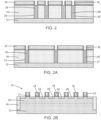
FIG. 2 is a cross-sectional view of the structure taken generally along line 2-2 inFIG. 1 . -
FIG. 2A is a cross-sectional view of the structure taken generally alongline 2A-2A inFIG. 1 . -
FIG. 2B is a cross-sectional view of the structure taken generally alongline 2B-2B inFIG. 1 . -
FIG. 3 is a top view of the structure at a fabrication stage of the processing method subsequent toFIG. 1 . -
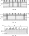
FIG. 4 is a cross-sectional view of the structure taken generally along line 4-4 inFIG. 3 . -
FIG. 4A is a cross-sectional view of the structure taken generally alongline 4A-4A inFIG. 3 . -
FIG. 4B is a cross-sectional view of the structure taken generally alongline 4B-4B inFIG. 3 . -
FIGS. 5 and 5A are cross-sectional views of a structure in accordance with alternative embodiments of the invention. -
FIGS. 6, 6A, and 6B are cross-sectional views of a structure in accordance with alternative embodiments of the invention. - With reference to
FIG. 1 ,2, 2A, 2B and in accordance with embodiments of the invention, adevice structure 10 includes a field-effect transistor 15 that may be formed using asubstrate 12 in the representative form of a bulk substrate. Thesubstrate 12 may be comprised of a semiconductor material, such as single-crystal silicon, and thesubstrate 12 may be doped (e.g., lightly doped) with a p-type dopant (e.g., boron) to provide p-type conductivity.Trench isolation regions 16 may be formed in thesubstrate 12. Thetrench isolation regions 16 surround an active region that is comprised of a portion of the semiconductor material of thesubstrate 12 and in which the field-effect transistor 15 is formed. Thetrench isolation regions 16 may be formed by a shallow trench isolation technique that patterns trenches in thesubstrate 12 with lithography and etching processes, deposits a dielectric material to overfill the trenches, and planarizes the dielectric material using chemical mechanical polishing and/or an etch back. The dielectric material contained in thetrench isolation regions 16 may be comprised of an electrical insulator, such as silicon dioxide. - The field-
effect transistor 15 may be fabricated by front-end-of-line processing in the active region of thesubstrate 12. In an embodiment, the field-effect transistor 15 may be deployed in a low-noise amplifier found in a radio-frequency circuit. In an embodiment, the field-effect transistor 15 may be deployed in a power amplifier found in a radio-frequency circuit. - The field-
effect transistor 15 may include a gate havingmultiple gate fingers 18, agate connector 20, and agate connector 22 that are disposed on a top surface of thesubstrate 12, as well as source/drain regions 24 and source/drain regions 26 that are disposed in thesubstrate 12. Thegate fingers 18 may be aligned parallel to each other, thegate fingers 18 may be connected at one end to thegate connector 20, and thegate fingers 18 may be connected at an opposite end to thegate connector 22. Thegate fingers 18 andgate connectors gate fingers 18 are patterned as elongate strips comprised of the conductor that extend from thegate connector 20 across the active region to thegate connector 22, and thegate connectors gate fingers 18. Thegate fingers 18 may have a length L, and eachgate finger 18 may extend longitudinally along alongitudinal axis 14 from aninner side edge 17 of thegate connector 20 to aninner side edge 19 of thegate connector 22. The inner side edges 17, 19 face each other across the active region. Thegate fingers 18 are arranged in the space over the active region between the inner side edges 17, 19. - The source/
drain regions 24 and the source/drain regions 26 are disposed in thesubstrate 12 between thegate fingers 18. The source/drain regions 24 and source/drain regions 26 may be formed by self-aligned ion implantation of a dopant (e.g., an n-type dopant) under given set of implantation conditions into thesubstrate 12. The implantation conditions (e.g., ion species, dose, kinetic energy) may be selected to tune the electrical and physical characteristics of the source/drain regions 24 and source/drain regions 26. In an embodiment, the source/drain regions 24 and source/drain regions 26 may contain semiconductor material that is doped with an n-type dopant (e.g., phosphorus and/or arsenic) to provide n-type conductivity. As used herein, the term "source/drain region" means a doped region of semiconductor material that can function as either a source or a drain of the field-effect transistor 15. In an embodiment, the source/drain regions 24 may define source regions of the field-effect transistor 15 and the source/drain regions 26 may define drain regions of the field-effect transistor 15. - A well 25 may be formed in the
substrate 12 before forming the source/drain regions 24 and source/drain regions 26. The well 25 may be formed by ion implantation of a dopant having an opposite conductivity type from the source/drain regions 24 and source/drain regions 26. A channel region constituted by a portion of the well 25 is arranged in thesubstrate 12 beneath eachgate finger 18 and laterally between each adjacent pair of source/drain regions effect transistor 15. - The field-
effect transistor 15 may include agate dielectric 21 disposed between thegate fingers 18 and thesubstrate 12, as well assidewall spacers 23 disposed on thegate fingers 18. In an embodiment, thegate dielectric 21 may be comprised of a dielectric material, such as silicon dioxide. In an embodiment, thesidewall spacers 23 may be comprised of a dielectric material, such as silicon nitride. - The
device structure 10 further includesbody contact regions 28 andbody contact regions 30 that are arranged at the periphery of the active region. Thebody contact regions effect transistor 15. Thebody contact regions 28 are disposed in respective lower portions ofopenings 29 that penetrate fully through thegate connector 20 and fully through thetrench isolation region 16 beneath thegate connector 20 to thesubstrate 12. Thebody contact regions 30 are disposed in respective lower portions ofopenings 31 that penetrate fully through thegate connector 22 and fully through thetrench isolation region 16 beneath thegate connector 22 to thesubstrate 12. - In an embodiment, the
body contact regions body contact regions openings gate connectors openings body contact regions trench isolation regions 16 during formation of thetrench isolation regions 16. In an embodiment, thebody contact regions body contact regions gate fingers 18. In an embodiment, thebody contact regions well 25. In an embodiment, thebody contact regions - The
body contact regions 28 are offset outwardly from theinner side edge 19 of thegate connector 20 to preserve the continuity of thegate connector 20 at the locations of thebody contact regions 28. Similarly, thebody contact regions 30 are offset outwardly from theinner side edge 19 of thegate connector 22 to preserve the continuity of thegate connector 22 at the locations of thebody contact regions 30. -
Spacers 35 may be formed on the sidewalls of thegate connector 20 bordering the upper portion of eachopening 29. Thespacers 35 may also be formed on the sidewalls of thegate connector 22 bordering the upper portion of eachopening 31. Thespacers 35 may be comprised of a dielectric material, such as silicon nitride, that is conformally deposited and anisotropically etched. - With reference to
FIGS. 3 ,4, 4A, 4B in which like reference numerals refer to like features inFIGS. 1 ,2, 2A, 2B and at a subsequent fabrication stage of the processing method, adielectric layer 34 may be formed, andsource contacts 36,drain contacts 38,gate contacts body contacts dielectric layer 34. Thedielectric layer 34 may be comprised of a dielectric material, such as silicon dioxide, that is an electrical insulator, and thesource contacts 36,drain contacts 38,gate contacts body contacts source contacts 36 penetrate through thedielectric layer 34 to land at a series of locations on each source/drain region 24. Similarly, thedrain contacts 38 penetrate through thedielectric layer 34 to land at a series of locations on each source/drain region 26. - The
gate contacts 40 are physically and electrically coupled to thegate connector 20, and thegate contacts 42 are physically and electrically coupled to thegate connector 22. In that regard, thegate contacts 40 penetrate through thedielectric layer 34 to land at a series of different locations on thegate connector 20, and thegate contacts 42 penetrate through thedielectric layer 34 to land at a series of different locations on thegate connector 22. - The
body contacts 44 are physically and electrically coupled to thebody contact regions 28, and thebody contacts 46 are physically and electrically coupled to thebody contact regions 30. In that regard, thebody contacts 44 penetrate through thedielectric layer 34 and the upper portions of theopenings 29 to land on thebody contact regions 28, and thebody contacts 46 penetrate through thedielectric layer 34 and the upper portions of theopenings 31 to land on thebody contact regions 30. Eachbody contact 44 penetrates through a portion of thegate connector 20 to one of thebody contact regions 28. Thespacers 35 are disposed between thebody contacts 44 and thegate connector 20 in the upper portions of theopenings 29 to provide electrical isolation. Eachbody contact 46 penetrates through a portion of thegate connector 22 to one of thebody contact regions 30. Thespacers 35 are also disposed between thebody contacts 46 and thegate connector 22 in the upper portions of theopenings 31 to provide electrical isolation. - The
gate contacts 40 and thebody contacts 44 are positioned with a spaced-apart arrangement and interleaved along the length of thegate connector 20 with thegate contacts 40 disposed adjacent to thebody contacts 44. In an embodiment, thegate contacts 40 may be intermingled and interleaved with thebody contacts 44 in an array (e.g., a row) along the length of thegate connector 20. In an embodiment, thegate contacts 40 and thebody contacts 44 may be arranged and interleaved in a pattern along the length of thegate connector 20. In an embodiment, the placement of thegate contacts 40 and thebody contacts 44 may vary along the length of thegate connector 20 and lack a pattern. In an embodiment, thebody contacts 44 and thebody contact regions 28 may be aligned with thegate fingers 18. In an embodiment, thebody contacts 44 and thebody contact regions 28 may be non-aligned with thegate fingers 18. In an embodiment, two or more of thebody contact regions 28 may be arranged immediately adjacent to each other such thecorresponding body contacts 44 are adjacent without interveninggate contacts 40. - The
gate contacts 42 and thebody contacts 46 are positioned with a spaced-apart arrangement along the length of thegate connector 22 with thegate contacts 42 disposed adjacent to thebody contacts 46. In an embodiment, thegate contacts 42 may be intermingled and interleaved with thebody contacts 46 in a row or an array along the length of thegate connector 22. In an embodiment, thegate contacts 42 and thebody contacts 46 may be arranged in a pattern along the length of thegate connector 22. In an embodiment, the placement of thegate contacts 42 and thebody contacts 46 may vary along the length of thegate connector 22 and lack a pattern. In an embodiment, one or more of thebody contact regions 30 andbody contacts 46 may be aligned with thegate fingers 18. In an embodiment, one or more of thebody contact regions 30 andbody contacts 46 may be non-aligned with thegate fingers 18. In an embodiment, two or more of thebody contact regions 30 may be arranged immediately adjacent to each other such thecorresponding body contacts 46 are adjacent without interveninggate contacts 42. - The
body contact regions body contacts effect transistor 15 to improve, for example, linearity and the third-order input intercept point during operation while maintaining a high threshold frequency. The interleaving of thebody contact regions 28 andbody contacts 44 beneath thegate connector 20 and thebody contact regions 30 andbody contacts 46 beneath thegate connector 22 at both sides of the active region may provide a low gate resistance and a low minimum noise factor. - With reference to
FIGS. 5, 5A and in accordance with alternative embodiments of the invention, thedevice structure 10 may include anexternal resistor 50 that is physically and electrically connected to thebody contacts 44 and anexternal resistor 52 that is physically and electrically connected to thebody contacts 46. Apower supply 54 may be coupled by theexternal resistor 50 to thebody contacts 44 and by theexternal resistor 52 to thebody contacts 46. Thepower supply 54 may be utilized, during operation of the field-effect transistor 15, to bias thebody contact regions - With reference to
FIGS. 6, 6A, 6B and in accordance with alternative embodiments of the invention, thedevice structure 10 may be formed using silicon-on-insulator substrate that includes adevice layer 62, a buriedoxide layer 64, and asemiconductor substrate 66. Thedevice layer 62 is separated from thesemiconductor substrate 66 by the intervening buriedoxide layer 64 and may be significantly thinner than thesemiconductor substrate 66. Thedevice layer 62 is electrically isolated from thesemiconductor substrate 66 by the buriedoxide layer 64. Thedevice layer 62 and thesemiconductor substrate 66 may be comprised of a semiconductor material, such as single-crystal silicon, and the buriedoxide layer 64 may be comprised of silicon dioxide. Thesemiconductor substrate 66 may be lightly doped to have, for example, p-type conductivity. Thetrench isolation regions 16 extend through thedevice layer 62 to the buriedoxide layer 64. - The
body contact regions device layer 62 that are contacted by thebody contacts device layer 62 are separated from thesemiconductor substrate 66 by the dielectric material of the buriedoxide layer 64. Eachbody contact region 28 is positioned adjacent to a portion of one of thetrench isolation regions 16. Adjacent pairs of thebody contact regions 28 are separated from each other by the dielectric material of thetrench isolation region 16. Eachbody contact region 30 is positioned adjacent to a portion of one of thetrench isolation regions 16. Adjacent pairs of thebody contact regions 30 are separated from each other by the dielectric material of thetrench isolation region 16. A portion of the buriedoxide layer 64 is disposed in a lateral direction between thebody contact region 28 and thebody contact region 30. - In an embodiment, each of the
body contact regions 28 may be aligned with one of thegate fingers 18. In an embodiment, each of thebody contact regions 30 may be aligned with one of thegate fingers 18. - The methods as described above are used in the fabrication of integrated circuit chips. The resulting integrated circuit chips can be distributed by the fabricator in raw wafer form (e.g., as a single wafer that has multiple unpackaged chips), as a bare die, or in a packaged form. The chip may be integrated with other chips, discrete circuit elements, and/or other signal processing devices as part of either an intermediate product or an end product. The end product can be any product that includes integrated circuit chips, such as computer products having a central processor or smartphones.
- References herein to terms modified by language of approximation, such as "about", "approximately", and "substantially", are not to be limited to the precise value specified. The language of approximation may correspond to the precision of an instrument used to measure the value and, unless otherwise dependent on the precision of the instrument, may indicate a range of +/- 10% of the stated value(s).
- References herein to terms such as "vertical", "horizontal", etc. are made by way of example, and not by way of limitation, to establish a frame of reference. The term "horizontal" as used herein is defined as a plane parallel to a conventional plane of a semiconductor substrate, regardless of its actual three-dimensional spatial orientation. The terms "vertical" and "normal" refer to a direction in the frame of reference perpendicular to the horizontal, as just defined. The term "lateral" refers to a direction in the frame of reference within the horizontal plane.
- A feature "connected" or "coupled" to or with another feature may be directly connected or coupled to or with the other feature or, instead, one or more intervening features may be present. A feature may be "directly connected" or "directly coupled" to or with another feature if intervening features are absent. A feature may be "indirectly connected" or "indirectly coupled" to or with another feature if at least one intervening feature is present. A feature "on" or "contacting" another feature may be directly on or in direct contact with the other feature or, instead, one or more intervening features may be present. A feature may be "directly on" or in "direct contact" with another feature if intervening features are absent. A feature may be "indirectly on" or in "indirect contact" with another feature if at least one intervening feature is present. Different features "overlap" if a feature extends over, and covers a part of, another feature.
- The descriptions of the various embodiments of the present invention have been presented for purposes of illustration but are not intended to be exhaustive or limited to the embodiments disclosed. Many modifications and variations will be apparent to those of ordinary skill in the art without departing from the scope and spirit of the described embodiments. The terminology used herein was chosen to best explain the principles of the embodiments, the practical application or technical improvement over technologies found in the marketplace, or to enable others of ordinary skill in the art to understand the embodiments disclosed herein.
Claims (15)
- A structure comprising:a substrate;a first trench isolation region in the substrate;a field-effect transistor including a first gate connector, a first gate finger that extends from the first gate connector, a second gate finger that extends from the first gate connector, and a source/drain region disposed between the first gate finger and the second gate finger, the first gate connector positioned over the first trench isolation region;a first body contact region that extends through the first trench isolation region to the substrate;a first gate contact coupled to the first gate connector; anda first body contact that penetrates through a first portion of the first gate connector to the first body contact region.
- The structure of claim 1 further comprising:
a dielectric spacer between the first body contact and the first portion of the first gate connector. - The structure of claim 1 or claim 2 further comprising:a second body contact region that extends through the first trench isolation region to the substrate; anda second body contact that penetrates through a second portion of the first gate connector to the second body contact region.
- The structure of claim 3 wherein the first trench isolation region comprises a dielectric material, and the first body contact region is separated from the second body contact region by the dielectric material of the first trench isolation region.
- The structure of claim 3 or claim 4 wherein the first body contact region is positioned adjacent to the second body contact region, and the first gate contact is positioned between the first body contact and the second body contact, or the first body contact is positioned between the first gate contact and the second body contact.
- The structure of one of claims 3 to 5 further comprising:a second gate contact coupled to the first gate connector,wherein the first body contact is positioned between the first gate contact and the second gate contact, and, optionally, wherein the first body contact, the second body contact, the first gate contact, and the second gate contact are interleaved in an array along a length of the first gate connector.
- The structure of one of claims 1 to 6 further comprising:a second trench isolation region in the substrate,wherein the field-effect transistor includes a second gate connector, the first gate finger extends longitudinally from the first gate connector to the second gate connector, the second gate finger extends longitudinally from the first gate connector to the second gate connector, and the second gate connector is positioned over the second trench isolation region.
- The structure of claim 7 further comprising:a third body contact region that extends through the second trench isolation region to the substrate; anda third body contact that penetrates through a portion of the second gate connector to the third body contact region, and, optionally, further comprisinga gate contact coupled to the second gate connector.
- The structure of one of claims 1 to 8 wherein the first body contact region comprises a doped semiconductor material disposed in an opening penetrating through the first trench isolation region, and/or wherein the first body contact region is aligned with the first gate finger.
- The structure of one of claims 1 to 9 further comprising:an external resistor; anda power supply coupled by the external resistor to the first body contact.
- The structure of claims 1 to 10 wherein the first gate finger and the second gate finger comprise a first semiconductor material having a first conductivity type, and the first body contact comprises a semiconductor material having a second conductivity type opposite to the first conductivity type.
- A structure comprising:a silicon-on-insulator substrate including a semiconductor layer, a semiconductor substrate, and a buried oxide layer between the semiconductor layer and the semiconductor substrate;an isolation region in the semiconductor layer;a field-effect transistor including a gate connector, a first gate finger that extends from the gate connector, a second gate finger that extends from the gate connector, and a source/drain region disposed between the first gate finger and the second gate finger, the gate connector positioned over the isolation region;a first body contact region comprising a first portion of the semiconductor layer that is adjacent to the isolation region;a gate contact coupled to the gate connector; anda first body contact that penetrates through a first portion of the gate connector to the first body contact region.
- The structure of claim 12 wherein the first body contact region is aligned with the first gate finger.
- The structure of claim 11 or claim 12 further comprising:a second body contact region comprising a second portion of the semiconductor layer that is adjacent to the isolation region; anda second contact that extends through a second portion of the gate connector to the second body contact region,wherein the isolation region comprises a dielectric material, and the first body contact region is separated from the second body contact region by the dielectric material of the isolation region.
- A method comprising:forming a trench isolation region in a substrate;forming a field-effect transistor including a gate connector, a first gate finger that extends from the gate connector, a second gate finger that extends from the gate connector, and a source/drain region disposed between the first gate finger and the second gate finger, wherein the gate connector is positioned over the trench isolation region;forming a body contact region that extends through the trench isolation region to the substrate;forming a gate contact coupled to the gate connector; andforming a body contact that penetrates through a first portion of the gate connector to the body contact region.
Applications Claiming Priority (1)
| Application Number | Priority Date | Filing Date | Title |
|---|---|---|---|
| US18/098,188 US12690248B2 (en) | 2023-01-18 | 2023-01-18 | Transistor structures with interleaved body contacts and gate contacts |
Publications (1)
| Publication Number | Publication Date |
|---|---|
| EP4404271A1 true EP4404271A1 (en) | 2024-07-24 |
Family
ID=89190746
Family Applications (1)
| Application Number | Title | Priority Date | Filing Date |
|---|---|---|---|
| EP23215717.2A Pending EP4404271A1 (en) | 2023-01-18 | 2023-12-12 | Transistor structures with interleaved body contacts and gate contacts |
Country Status (3)
| Country | Link |
|---|---|
| US (1) | US12690248B2 (en) |
| EP (1) | EP4404271A1 (en) |
| CN (1) | CN118366989A (en) |
Families Citing this family (1)
| Publication number | Priority date | Publication date | Assignee | Title |
|---|---|---|---|---|
| US12349444B1 (en) * | 2024-04-11 | 2025-07-01 | Globalfoundries Singapore Pte. Ltd | Under-source body contact |
Citations (3)
| Publication number | Priority date | Publication date | Assignee | Title |
|---|---|---|---|---|
| US20070034903A1 (en) * | 2003-10-22 | 2007-02-15 | Sehat Sutardja | Efficient transistor structure |
| DE102014224846A1 (en) * | 2014-12-04 | 2016-06-09 | Infineon Technologies Ag | FET device |
| US20170287836A1 (en) * | 2016-03-31 | 2017-10-05 | Skyworks Solutions, Inc. | Non-symmetric body contacts for field-effect transistors |
Family Cites Families (4)
| Publication number | Priority date | Publication date | Assignee | Title |
|---|---|---|---|---|
| US10424664B2 (en) | 2016-12-14 | 2019-09-24 | Globalfoundries Inc. | Poly gate extension source to body contact |
| US10573724B2 (en) | 2018-04-10 | 2020-02-25 | International Business Machines Corporation | Contact over active gate employing a stacked spacer |
| US20200373410A1 (en) | 2019-05-26 | 2020-11-26 | Globalfoundries Inc. | Contact structures over an active region of a semiconductor device |
| US11411077B2 (en) * | 2020-09-10 | 2022-08-09 | Semiconductor Components Industries, Llc | Electronic device including doped regions and a trench between the doped regions |
-
2023
- 2023-01-18 US US18/098,188 patent/US12690248B2/en active Active
- 2023-12-01 CN CN202311635974.2A patent/CN118366989A/en active Pending
- 2023-12-12 EP EP23215717.2A patent/EP4404271A1/en active Pending
Patent Citations (3)
| Publication number | Priority date | Publication date | Assignee | Title |
|---|---|---|---|---|
| US20070034903A1 (en) * | 2003-10-22 | 2007-02-15 | Sehat Sutardja | Efficient transistor structure |
| DE102014224846A1 (en) * | 2014-12-04 | 2016-06-09 | Infineon Technologies Ag | FET device |
| US20170287836A1 (en) * | 2016-03-31 | 2017-10-05 | Skyworks Solutions, Inc. | Non-symmetric body contacts for field-effect transistors |
Also Published As
| Publication number | Publication date |
|---|---|
| US20240243175A1 (en) | 2024-07-18 |
| US12690248B2 (en) | 2026-07-21 |
| CN118366989A (en) | 2024-07-19 |
Similar Documents
| Publication | Publication Date | Title |
|---|---|---|
| US7138690B2 (en) | Shielding structure for use in a metal-oxide-semiconductor device | |
| US10665551B2 (en) | Trench MOSFET device and the preparation method thereof | |
| EP0810647A2 (en) | Process for forming a self-aligned raised source/drain MOS device and device therefrom | |
| US5970356A (en) | Method for fabricating a bipolar transistor | |
| KR20210011671A (en) | Lateral double diffused metal oxide semiconductor and method for fabricating the same | |
| JPH1064994A (en) | Semiconductor device | |
| US8742538B2 (en) | SiGe HBT and manufacturing method thereof | |
| US20240243175A1 (en) | Transistor structures with interleaved body contacts and gate contacts | |
| CN117317006A (en) | Laterally diffused metal oxide semiconductor device with field plate | |
| US20190221643A1 (en) | Semiconductor device formed on a soi substrate | |
| US12191351B1 (en) | Laterally-diffused metal-oxide-semiconductor devices with an air gap | |
| US20020140030A1 (en) | SOI devices with integrated gettering structure | |
| EP4415051A1 (en) | Field-effect transistors with self-aligned p-shield contacts | |
| US12424493B2 (en) | Self-aligned double patterning with mandrel manipulation | |
| US11935946B2 (en) | Silicon-controlled rectifiers in a silicon-on-insulator technology | |
| EP4354511A2 (en) | Device with field plates | |
| CN118676143A (en) | Transistor structure, radio frequency front-end device and electronic equipment | |
| US11081561B2 (en) | Field-effect transistors with vertically-serpentine gates | |
| US12243923B2 (en) | Contact-over-active-gate transistor structures with contacts landed on enlarged gate portions | |
| US11545548B1 (en) | Gate contacts with airgap isolation | |
| US12408396B1 (en) | Field-effect transistors with heterogenous doped regions in the substrate of a silicon-on-insulator substrate | |
| EP4496006A1 (en) | Extended-drain metal-oxide-semiconductor devices with a dual-thickness gate dielectric layer | |
| US12205949B1 (en) | High-voltage semiconductor device structures | |
| US11721621B2 (en) | Stacked field-effect transistors with a shielded output | |
| US12451446B2 (en) | RFLDMOS device and manufacturing method thereof |
Legal Events
| Date | Code | Title | Description |
|---|---|---|---|
| PUAI | Public reference made under article 153(3) epc to a published international application that has entered the european phase |
Free format text: ORIGINAL CODE: 0009012 |
|
| STAA | Information on the status of an ep patent application or granted ep patent |
Free format text: STATUS: THE APPLICATION HAS BEEN PUBLISHED |
|
| AK | Designated contracting states |
Kind code of ref document: A1 Designated state(s): AL AT BE BG CH CY CZ DE DK EE ES FI FR GB GR HR HU IE IS IT LI LT LU LV MC ME MK MT NL NO PL PT RO RS SE SI SK SM TR |
|
| STAA | Information on the status of an ep patent application or granted ep patent |
Free format text: STATUS: REQUEST FOR EXAMINATION WAS MADE |
|
| 17P | Request for examination filed |
Effective date: 20241203 |
|
| RBV | Designated contracting states (corrected) |
Designated state(s): AL AT BE BG CH CY CZ DE DK EE ES FI FR GB GR HR HU IE IS IT LI LT LU LV MC ME MK MT NL NO PL PT RO RS SE SI SK SM TR |