EP4404270A1 - Field-effect transistors formed using a wide bandgap semiconductor material - Google Patents
Field-effect transistors formed using a wide bandgap semiconductor material Download PDFInfo
- Publication number
- EP4404270A1 EP4404270A1 EP23205075.7A EP23205075A EP4404270A1 EP 4404270 A1 EP4404270 A1 EP 4404270A1 EP 23205075 A EP23205075 A EP 23205075A EP 4404270 A1 EP4404270 A1 EP 4404270A1
- Authority
- EP
- European Patent Office
- Prior art keywords
- layer
- hardmask
- top surface
- semiconductor substrate
- gate conductor
- Prior art date
- Legal status (The legal status is an assumption and is not a legal conclusion. Google has not performed a legal analysis and makes no representation as to the accuracy of the status listed.)
- Pending
Links
Images


Classifications
-
- H—ELECTRICITY
- H10—SEMICONDUCTOR DEVICES; ELECTRIC SOLID-STATE DEVICES NOT OTHERWISE PROVIDED FOR
- H10D—INORGANIC ELECTRIC SEMICONDUCTOR DEVICES
- H10D48/00—Individual devices not covered by groups H10D1/00 - H10D44/00
- H10D48/01—Manufacture or treatment
- H10D48/031—Manufacture or treatment of three-or-more electrode devices
-
- H—ELECTRICITY
- H10—SEMICONDUCTOR DEVICES; ELECTRIC SOLID-STATE DEVICES NOT OTHERWISE PROVIDED FOR
- H10D—INORGANIC ELECTRIC SEMICONDUCTOR DEVICES
- H10D30/00—Field-effect transistors [FET]
- H10D30/60—Insulated-gate field-effect transistors [IGFET]
- H10D30/64—Double-diffused metal-oxide semiconductor [DMOS] FETs
- H10D30/65—Lateral DMOS [LDMOS] FETs
- H10D30/658—Lateral DMOS [LDMOS] FETs having trench gate electrodes
-
- H—ELECTRICITY
- H10—SEMICONDUCTOR DEVICES; ELECTRIC SOLID-STATE DEVICES NOT OTHERWISE PROVIDED FOR
- H10D—INORGANIC ELECTRIC SEMICONDUCTOR DEVICES
- H10D30/00—Field-effect transistors [FET]
- H10D30/01—Manufacture or treatment
- H10D30/021—Manufacture or treatment of FETs having insulated gates [IGFET]
- H10D30/025—Manufacture or treatment of FETs having insulated gates [IGFET] of vertical IGFETs
-
- H—ELECTRICITY
- H10—SEMICONDUCTOR DEVICES; ELECTRIC SOLID-STATE DEVICES NOT OTHERWISE PROVIDED FOR
- H10D—INORGANIC ELECTRIC SEMICONDUCTOR DEVICES
- H10D30/00—Field-effect transistors [FET]
- H10D30/01—Manufacture or treatment
- H10D30/021—Manufacture or treatment of FETs having insulated gates [IGFET]
- H10D30/028—Manufacture or treatment of FETs having insulated gates [IGFET] of double-diffused metal oxide semiconductor [DMOS] FETs
- H10D30/0281—Manufacture or treatment of FETs having insulated gates [IGFET] of double-diffused metal oxide semiconductor [DMOS] FETs of lateral DMOS [LDMOS] FETs
- H10D30/0289—Manufacture or treatment of FETs having insulated gates [IGFET] of double-diffused metal oxide semiconductor [DMOS] FETs of lateral DMOS [LDMOS] FETs using recessing of the gate electrodes, e.g. to form trench gate electrodes
-
- H—ELECTRICITY
- H10—SEMICONDUCTOR DEVICES; ELECTRIC SOLID-STATE DEVICES NOT OTHERWISE PROVIDED FOR
- H10D—INORGANIC ELECTRIC SEMICONDUCTOR DEVICES
- H10D30/00—Field-effect transistors [FET]
- H10D30/01—Manufacture or treatment
- H10D30/021—Manufacture or treatment of FETs having insulated gates [IGFET]
- H10D30/028—Manufacture or treatment of FETs having insulated gates [IGFET] of double-diffused metal oxide semiconductor [DMOS] FETs
- H10D30/0291—Manufacture or treatment of FETs having insulated gates [IGFET] of double-diffused metal oxide semiconductor [DMOS] FETs of vertical DMOS [VDMOS] FETs
- H10D30/0293—Manufacture or treatment of FETs having insulated gates [IGFET] of double-diffused metal oxide semiconductor [DMOS] FETs of vertical DMOS [VDMOS] FETs using formation of insulating sidewall spacers
-
- H—ELECTRICITY
- H10—SEMICONDUCTOR DEVICES; ELECTRIC SOLID-STATE DEVICES NOT OTHERWISE PROVIDED FOR
- H10D—INORGANIC ELECTRIC SEMICONDUCTOR DEVICES
- H10D30/00—Field-effect transistors [FET]
- H10D30/01—Manufacture or treatment
- H10D30/021—Manufacture or treatment of FETs having insulated gates [IGFET]
- H10D30/028—Manufacture or treatment of FETs having insulated gates [IGFET] of double-diffused metal oxide semiconductor [DMOS] FETs
- H10D30/0291—Manufacture or treatment of FETs having insulated gates [IGFET] of double-diffused metal oxide semiconductor [DMOS] FETs of vertical DMOS [VDMOS] FETs
- H10D30/0297—Manufacture or treatment of FETs having insulated gates [IGFET] of double-diffused metal oxide semiconductor [DMOS] FETs of vertical DMOS [VDMOS] FETs using recessing of the gate electrodes, e.g. to form trench gate electrodes
-
- H—ELECTRICITY
- H10—SEMICONDUCTOR DEVICES; ELECTRIC SOLID-STATE DEVICES NOT OTHERWISE PROVIDED FOR
- H10D—INORGANIC ELECTRIC SEMICONDUCTOR DEVICES
- H10D30/00—Field-effect transistors [FET]
- H10D30/60—Insulated-gate field-effect transistors [IGFET]
- H10D30/63—Vertical IGFETs
-
- H—ELECTRICITY
- H10—SEMICONDUCTOR DEVICES; ELECTRIC SOLID-STATE DEVICES NOT OTHERWISE PROVIDED FOR
- H10D—INORGANIC ELECTRIC SEMICONDUCTOR DEVICES
- H10D30/00—Field-effect transistors [FET]
- H10D30/60—Insulated-gate field-effect transistors [IGFET]
- H10D30/64—Double-diffused metal-oxide semiconductor [DMOS] FETs
- H10D30/66—Vertical DMOS [VDMOS] FETs
- H10D30/668—Vertical DMOS [VDMOS] FETs having trench gate electrodes, e.g. UMOS transistors
-
- H—ELECTRICITY
- H10—SEMICONDUCTOR DEVICES; ELECTRIC SOLID-STATE DEVICES NOT OTHERWISE PROVIDED FOR
- H10D—INORGANIC ELECTRIC SEMICONDUCTOR DEVICES
- H10D62/00—Semiconductor bodies, or regions thereof, of devices having potential barriers
- H10D62/10—Shapes, relative sizes or dispositions of the regions of the semiconductor bodies; Shapes of the semiconductor bodies
- H10D62/102—Constructional design considerations for preventing surface leakage or controlling electric field concentration
- H10D62/103—Constructional design considerations for preventing surface leakage or controlling electric field concentration for increasing or controlling the breakdown voltage of reverse-biased devices
- H10D62/105—Constructional design considerations for preventing surface leakage or controlling electric field concentration for increasing or controlling the breakdown voltage of reverse-biased devices by having particular doping profiles, shapes or arrangements of PN junctions; by having supplementary regions, e.g. junction termination extension [JTE]
- H10D62/106—Constructional design considerations for preventing surface leakage or controlling electric field concentration for increasing or controlling the breakdown voltage of reverse-biased devices by having particular doping profiles, shapes or arrangements of PN junctions; by having supplementary regions, e.g. junction termination extension [JTE] having supplementary regions doped oppositely to or in rectifying contact with regions of the semiconductor bodies, e.g. guard rings with PN or Schottky junctions
- H10D62/107—Buried supplementary regions, e.g. buried guard rings
-
- H—ELECTRICITY
- H10—SEMICONDUCTOR DEVICES; ELECTRIC SOLID-STATE DEVICES NOT OTHERWISE PROVIDED FOR
- H10D—INORGANIC ELECTRIC SEMICONDUCTOR DEVICES
- H10D62/00—Semiconductor bodies, or regions thereof, of devices having potential barriers
- H10D62/80—Semiconductor bodies, or regions thereof, of devices having potential barriers characterised by the materials
- H10D62/83—Semiconductor bodies, or regions thereof, of devices having potential barriers characterised by the materials being Group IV materials, e.g. B-doped Si or undoped Ge
- H10D62/8303—Diamond
-
- H—ELECTRICITY
- H10—SEMICONDUCTOR DEVICES; ELECTRIC SOLID-STATE DEVICES NOT OTHERWISE PROVIDED FOR
- H10D—INORGANIC ELECTRIC SEMICONDUCTOR DEVICES
- H10D62/00—Semiconductor bodies, or regions thereof, of devices having potential barriers
- H10D62/80—Semiconductor bodies, or regions thereof, of devices having potential barriers characterised by the materials
- H10D62/83—Semiconductor bodies, or regions thereof, of devices having potential barriers characterised by the materials being Group IV materials, e.g. B-doped Si or undoped Ge
- H10D62/832—Semiconductor bodies, or regions thereof, of devices having potential barriers characterised by the materials being Group IV materials, e.g. B-doped Si or undoped Ge being Group IV materials comprising two or more elements, e.g. SiGe
- H10D62/8325—Silicon carbide
-
- H—ELECTRICITY
- H10—SEMICONDUCTOR DEVICES; ELECTRIC SOLID-STATE DEVICES NOT OTHERWISE PROVIDED FOR
- H10D—INORGANIC ELECTRIC SEMICONDUCTOR DEVICES
- H10D64/00—Electrodes of devices having potential barriers
- H10D64/20—Electrodes characterised by their shapes, relative sizes or dispositions
- H10D64/27—Electrodes not carrying the current to be rectified, amplified, oscillated or switched, e.g. gates
- H10D64/311—Gate electrodes for field-effect devices
- H10D64/411—Gate electrodes for field-effect devices for FETs
- H10D64/511—Gate electrodes for field-effect devices for FETs for IGFETs
- H10D64/512—Disposition of the gate electrodes, e.g. buried gates
- H10D64/513—Disposition of the gate electrodes, e.g. buried gates within recesses in the substrate, e.g. trench gates, groove gates or buried gates
-
- H—ELECTRICITY
- H10—SEMICONDUCTOR DEVICES; ELECTRIC SOLID-STATE DEVICES NOT OTHERWISE PROVIDED FOR
- H10D—INORGANIC ELECTRIC SEMICONDUCTOR DEVICES
- H10D64/00—Electrodes of devices having potential barriers
- H10D64/20—Electrodes characterised by their shapes, relative sizes or dispositions
- H10D64/27—Electrodes not carrying the current to be rectified, amplified, oscillated or switched, e.g. gates
- H10D64/311—Gate electrodes for field-effect devices
- H10D64/411—Gate electrodes for field-effect devices for FETs
- H10D64/511—Gate electrodes for field-effect devices for FETs for IGFETs
- H10D64/517—Gate electrodes for field-effect devices for FETs for IGFETs characterised by the conducting layers
- H10D64/519—Gate electrodes for field-effect devices for FETs for IGFETs characterised by the conducting layers characterised by their top-view geometrical layouts
-
- H—ELECTRICITY
- H10—SEMICONDUCTOR DEVICES; ELECTRIC SOLID-STATE DEVICES NOT OTHERWISE PROVIDED FOR
- H10P—GENERIC PROCESSES OR APPARATUS FOR THE MANUFACTURE OR TREATMENT OF DEVICES COVERED BY CLASS H10
- H10P14/00—Formation of materials, e.g. in the shape of layers or pillars
- H10P14/40—Formation of materials, e.g. in the shape of layers or pillars of conductive or resistive materials
- H10P14/412—Deposition of metallic or metal-silicide materials
- H10P14/414—Deposition of metallic or metal-silicide materials of metal-silicide materials
-
- H—ELECTRICITY
- H10—SEMICONDUCTOR DEVICES; ELECTRIC SOLID-STATE DEVICES NOT OTHERWISE PROVIDED FOR
- H10P—GENERIC PROCESSES OR APPARATUS FOR THE MANUFACTURE OR TREATMENT OF DEVICES COVERED BY CLASS H10
- H10P14/00—Formation of materials, e.g. in the shape of layers or pillars
- H10P14/60—Formation of materials, e.g. in the shape of layers or pillars of insulating materials
- H10P14/63—Formation of materials, e.g. in the shape of layers or pillars of insulating materials characterised by the formation processes
- H10P14/6302—Non-deposition formation processes
- H10P14/6304—Formation by oxidation, e.g. oxidation of the substrate
- H10P14/6314—Formation by oxidation, e.g. oxidation of the substrate of a metallic layer
-
- H—ELECTRICITY
- H10—SEMICONDUCTOR DEVICES; ELECTRIC SOLID-STATE DEVICES NOT OTHERWISE PROVIDED FOR
- H10P—GENERIC PROCESSES OR APPARATUS FOR THE MANUFACTURE OR TREATMENT OF DEVICES COVERED BY CLASS H10
- H10P76/00—Manufacture or treatment of masks on semiconductor bodies, e.g. by lithography or photolithography
- H10P76/40—Manufacture or treatment of masks on semiconductor bodies, e.g. by lithography or photolithography of masks comprising inorganic materials
- H10P76/405—Manufacture or treatment of masks on semiconductor bodies, e.g. by lithography or photolithography of masks comprising inorganic materials characterised by their composition, e.g. multilayer masks
-
- H—ELECTRICITY
- H10—SEMICONDUCTOR DEVICES; ELECTRIC SOLID-STATE DEVICES NOT OTHERWISE PROVIDED FOR
- H10D—INORGANIC ELECTRIC SEMICONDUCTOR DEVICES
- H10D64/00—Electrodes of devices having potential barriers
- H10D64/01—Manufacture or treatment
- H10D64/011—Manufacture or treatment of electrodes ohmically coupled to a semiconductor
- H10D64/0111—Manufacture or treatment of electrodes ohmically coupled to a semiconductor to Group IV semiconductors
- H10D64/0112—Manufacture or treatment of electrodes ohmically coupled to a semiconductor to Group IV semiconductors using conductive layers comprising silicides
Definitions
- the disclosure relates to semiconductor devices and integrated circuit manufacture and, more specifically, to structures for a field-effect transistor and methods of forming such structures.
- Wide bandgap semiconductors such as silicon carbide
- Silicon carbide is well suited for power switching because of its advantageous properties, such as a high saturated drift velocity, a high critical field strength, an exceptional thermal conductivity, and a significant mechanical strength.
- a metal-oxide-semiconductor field-effect transistor is a type of gate-voltage-controlled power switching device that uses field inversion as a current control mechanism.
- a metal-oxide-semiconductor field-effect transistor may leverage the favorable properties of a silicon carbide substrate to enable, for example, power converters, motor inverters, and motor drivers that are characterized by high reliability and high efficiency when operating at a high voltage.
- a structure for a field-effect transistor comprises a semiconductor substrate including a top surface, a doped region adjacent to the top surface, and a trench that extends through the doped region.
- the semiconductor substrate comprises a wide bandgap semiconductor material.
- the structure further comprises a gate structure including a gate conductor layer.
- the gate conductor layer has a first portion disposed above the top surface of the semiconductor substrate and a second portion disposed inside the trench below the top surface of the semiconductor substrate.
- the gate structure may further include a silicide layer on the first portion of the gate conductor layer.
- the silicide layer and the trench may have substantially equal width dimensions.
- the gate conductor layer may extend through the doped region.
- the structure may further comprise a dielectric layer on the first portion of the gate conductor layer.
- the dielectric layer and the trench may have substantially equal width dimensions.
- the structure may additionally comprise a dielectric spacer on the dielectric layer.
- the wide bandgap semiconductor material may comprise silicon carbide.
- a method of forming a structure for a field-effect transistor comprises forming a doped region in a semiconductor substrate adjacent to a top surface of the semiconductor substrate, forming a trench in the semiconductor substrate, and forming a gate structure including a gate conductor layer.
- the semiconductor substrate comprises a wide bandgap semiconductor material, the trench extends through the doped region, and the gate conductor layer has a first portion disposed above the top surface of the semiconductor substrate and a second portion disposed inside the trench below the top surface of the semiconductor substrate.
- the step of forming the trench in the semiconductor substrate may comprise forming a hardmask on the top surface of the semiconductor substrate, wherein the trench extends through the hardmask into the semiconductor substrate.
- the method may further comprise forming a silicide layer on the first portion of the gate conductor layer, and removing the hardmask after forming the silicide layer.
- the method may further comprise recessing the gate conductor layer relative to a top surface of the hardmask.
- the recessed gate conductor layer may have a top surface disposed between the top surface of the hardmask and the top surface of the semiconductor substrate.
- the method may additionally comprise forming a silicide layer on the gate conductor layer, forming a dielectric layer inside a portion of the trench over the silicide layer and the gate conductor layer, and removing the hardmask after forming the silicide layer and the dielectric layer.
- the method may further comprise recessing the gate conductor layer relative to a top surface of the hardmask, and forming a dielectric layer inside a portion of the trench over the gate conductor layer.
- the method may further comprise removing the hardmask after forming the gate structure; and forming a dielectric layer by an oxidation process on the gate conductor layer after removing the hardmask.
- the hardmask may comprise a material having a melting point that is greater than or equal to 2000 °C.
- the hardmask may comprise aluminum nitride, or polycrystalline silicon carbide.
- the hardmask may include a first layer and a second layer that is disposed on the first layer.
- the first layer may comprise aluminum oxide
- the second layer may comprise aluminum nitride or polycrystalline silicon carbide.
- the first layer may comprise aluminum nitride
- the second layer may comprise polycrystalline silicon carbide.
- a structure 10 for a field-effect transistor may be formed using a semiconductor substrate 11 that includes a bulk substrate 12 and a semiconductor layer 14 formed by, for example, epitaxial growth on the bulk substrate 12.
- the semiconductor layer 14 of the semiconductor substrate 11 may be comprised of a wide bandgap semiconductor material, such as silicon carbide.
- the bulk substrate 12 of the semiconductor substrate 11 may be comprised of a wide bandgap semiconductor material.
- the semiconductor substrate 11 may be comprised of silicon carbide, which is a wide bandgap semiconductor material.
- the semiconductor substrate 11 may be comprised of diamond, which is a wide bandgap semiconductor material.
- the semiconductor layer 14 may include a buffer sublayer grown directly on the bulk substrate 12 and a drift sublayer grown on the buffer sublayer, and the drift sublayer may have a dopant concentration and a thickness that are optimized for device operation in a 650 volt to 1200 volt range.
- the bulk substrate 12 may operate as the drain of the field-effect transistor.
- a doped region 16 may be formed in the semiconductor layer 14 adjacent to a top surface 13 of the semiconductor substrate 11.
- the doped region 16 is doped to have an opposite conductivity type from the semiconductor layer 14.
- the doped region 16 has a lower boundary that defines an interface with the underlying semiconductor material of the semiconductor layer 14 across which the dopant type changes.
- the doped region 16 may define a body of the field-effect transistor.
- the doped region 16 may be formed by introducing a dopant of a given conductivity type by, for example, ion implantation into the semiconductor layer 14.
- An implantation mask may be formed to define a selected area on a top surface 13 of the semiconductor substrate 11 that is exposed for the implantation of ions.
- the implantation mask may include a hardmask that is applied and patterned to form an opening exposing the selected area on the top surface 13 and determining, at least in part, the location and horizontal dimensions of the doped region 16.
- the implantation conditions e.g., ion species, dose, kinetic energy, substrate temperature
- the ion implantation may be performed at substrate temperature in a range of 200°C to 600°C to minimize defect formation.
- the implantation mask which is compatible with the implantation conditions and is stripped following implantation, has a thickness and stopping power sufficient to block the implantation of ions in masked areas.
- the doped region 16 may be doped with a concentration of a p-type dopant (e.g., aluminum) to provide p-type electrical conductivity.
- Contacts 19 may be formed at the periphery of the doped region 16.
- the contacts 19 may be formed by ion implantation using an implantation mask, and the contacts 19 may have the same conductivity type (e.g., p-type) as the doped region 16 but at a higher dopant concentration.
- the contacts 19 may provide body contacts to the body of the field-effect transistor defined by the doped region 16.
- a doped region 18 may be formed in the semiconductor layer 14 adjacent to a top surface 13 of the semiconductor substrate 11.
- the doped region 18 has the same conductivity type as the semiconductor layer 14 but at a higher dopant concentration.
- the doped region 18 has an upper boundary that may be coplanar or substantially coplanar with the top surface 13 of the semiconductor substrate 11 and a lower boundary that defines an interface with the doped region 16 across which the conductivity type changes.
- the doped region 18 may define a source of the field-effect transistor.
- the doped region 18 may be formed by introducing a dopant of a given conductivity type by, for example, ion implantation into the semiconductor layer 14.
- An implantation mask may be formed to define a selected area on a top surface 13 of the semiconductor substrate 11 that is exposed for the implantation of ions.
- the implantation mask may include a hardmask that is applied and patterned to form an opening exposing the selected area on the top surface 13 of the semiconductor substrate 11 and determining, at least in part, the location and horizontal dimensions of the doped region 18.
- the implantation conditions e.g., ion species, dose, kinetic energy, substrate temperature
- the ion implantation may be performed at substrate temperature in a range of 200°C to 600°C to minimize defect formation.
- the implantation mask which is compatible with the implantation conditions and is stripped following implantation, has a thickness and stopping power sufficient to block the implantation of ions in masked areas.
- the doped region 18 may be doped with a concentration of an n-type dopant (e.g., nitrogen and/or phosphorus) to provide n-type electrical conductivity.
- the doped region 18 may be doped with a higher concentration of the n-type dopant than the semiconductor layer 14.
- a hardmask 20 is applied on the top surface 13 of the semiconductor substrate 11 and, in particular, the hardmask 20 may be disposed on the top surface 13 over the doped regions 16, 18.
- the hardmask 20 may be comprised of a material that is characterized by a high melting point.
- the hardmask 20 may be comprised of a material that is characterized by a melting point greater than or equal to 2000°C.
- the hardmask 20 may be comprised of a material that is an electrical insulator and that is characterized by a melting point greater than or equal to 2000°C.
- the hardmask 20 may be comprised of a material that is an insulating ceramic having a melting point greater than or equal to 2000°C.
- the hardmask 20 may be comprised of a material that is a high-resistivity semiconductor material having a melting point greater than or equal to 2000°C. In an embodiment, the hardmask 20 may be comprised of a material characterized by a coefficient of thermal expansion that is similar to the coefficient of thermal expansion of crystalline silicon carbide.
- the hardmask 20 may include one or more layers each comprised of a material that is characterized by a melting point greater than or equal to 2000°C.
- the hardmask 20 may include a layer comprised of aluminum nitride.
- the hardmask 20 may include a layer comprised of polycrystalline silicon carbide.
- the hardmask 20 may include a layer comprised of either aluminum nitride or polycrystalline silicon carbide that is disposed on a layer comprised of aluminum oxide.
- the hardmask 20 may include a layer comprised of polycrystalline silicon carbide that is disposed on a layer comprised of aluminum nitride.
- each trench 22 includes an upper portion that extends through the hardmask 20 and a lower portion that extends from the top surface 13 of the semiconductor substrate 11 through both of the doped regions 16, 18 and into the semiconductor layer 14 beneath the doped region 16.
- Each trench 22, which may have a width dimension W, has a sidewall 24 and a trench bottom 26 that is positioned between the top surface 13 and the interface between the bulk substrate 12 and the semiconductor layer 14.
- the hardmask 20 is not removed from the top surface 13 after the trenches 22 are formed.
- a doped region 28 may be formed in the semiconductor layer 14 beneath the trench bottom 26 of each of the trenches 22.
- the doped regions 28 are positioned in a vertical direction between the trenches 22 and the bulk substrate 12 operating as the drain of the field-effect transistor.
- the doped regions 28 have an opposite conductivity type from the semiconductor layer 14 and the doped region 16.
- the doped regions 28 may participate in defining a p-shield of the field-effect transistor.
- the doped regions 28 may be formed by introducing a dopant of a given conductivity type by, for example, ion implantation into the semiconductor layer 14.
- the trenches 22 in the hardmask 20 may determine, at least in part, the location and horizontal dimensions of the doped regions 28.
- the hardmask 20 has a thickness and stopping power sufficient to block the implantation of ions in masked areas.
- the implantation conditions e.g., ion species, dose, kinetic energy, substrate temperature
- the doped regions 28 may be doped with a concentration of a p-type dopant (e.g., aluminum) to provide p-type electrical conductivity.
- a high-temperature anneal may be performed following the implantations to activate the implanted dopants and to alleviate post-implantation crystal damage.
- the high-temperature anneal may be performed with a removable carbon capping layer applied as a temporary coating on the hardmask 20 and at a high temperature, such as a temperature in a range of 1600°C to 1900°C.
- the hardmask 20, which can withstand the high anneal temperature, is disposed on the top surface 13 during the anneal and functions to enhance the surface protection during the anneal.
- the removable carbon capping layer may prevent silicon outgassing from surface areas, such as those surface areas inside the trenches 22, that are not covered and protected by the hardmask 20 during the high-temperature anneal.
- the carbon capping layer which may be comprised of burned photoresist or a deposited layer of carbon, is removed following the high-temperature anneal. In a conventional process flow, all hardmasks are removed before the high-temperature anneal.
- a gate structure including a gate dielectric layer 32 and a gate conductor layer 34 is formed inside each of the trenches 22.
- the gate conductor layers 34 may be comprised of polysilicon that is heavily doped with an n-type dopant, such as phosphorus or arsenic, and the gate dielectric layers 32 may be comprised of a dielectric material, such as silicon dioxide, that is an electrical insulator.
- the gate dielectric layer 32 and the gate conductor layer 34 may be recessed by an etching process such that the top surface 36 of each gate conductor layer 34 is disposed within the trenches 22 below the top surface 21 of the hardmask 20.
- the top surface 36 of each gate conductor layer 34 may be disposed in a vertical direction between the top surface 21 of the hardmask 20 and the top surface 13 of the semiconductor substrate 11.
- Each gate conductor layer 34 has an upper portion disposed above the top surface 13 of the semiconductor substrate 11 and a lower portion disposed in one of the trenches 22 below the top surface 13 of the semiconductor substrate 11. The upper and lower portions of each gate conductor layer 34 are disposed on opposite sides of the top surface 13 of the semiconductor substrate 11.
- dielectric layers 38 are formed in the open spaces inside the trenches 22 over the recessed gate conductor layers 34.
- the dielectric layers 38 may be comprised of a dielectric material, such as silicon dioxide, that is an electrical insulator.
- the dielectric layers 38 may be formed by depositing a dielectric material and polishing the dielectric material by chemical mechanical polishing to be coplanar or substantially coplanar with the top surface 21 of the hardmask 20.
- the formation of the dielectric layers 38 may include oxidizing the material of the gate conductor layers 34 by an oxidation process and polishing the oxidized material. The oxidation temperature may be selected in order to maximize the oxidation of the material constituting the gate conductor layers 34 and to minimize the oxidation of surrounding materials, such as the material of the hardmask 20.
- the dielectric layers 38 may have a top surface 39 that is coplanar or substantially coplanar with the top surface 21 of the hardmask 20. Due to the spatial constraint imposed by the upper portions of the trenches 22 in the hardmask 20, the dielectric layers 38 may have a width dimension that is equal or substantially equal to the width dimension W of the trenches 22. The formation of the dielectric layers 38 inside the upper portions of the trenches 22 may enable an increase in the thickness of the dielectric layers 38.
- the hardmask 20 may be removed from the top surface 13 by an etching process.
- the removal of the hardmask 20 reveals the top surface 13 of the semiconductor substrate 11 and provides access for contacting the doped regions 16, 18.
- the hardmask 20 may be removed without disturbing the dielectric layers 38, which are also revealed when the hardmask 20 is removed.
- Dielectric spacers 40 may be formed on the sidewalls of the dielectric layers 38.
- the dielectric spacers 40 may be comprised of a dielectric material, such as silicon nitride, silicon oxynitride, or silicon dioxide, that is an electrical insulator and that is conformally deposited and then anisotropically etched.
- the dielectric spacers 40 may be omitted from the structure 10.
- Middle-of-line processing and back-end-of-line processing may follow, which includes formation of silicide, contacts, vias, and wiring for an interconnect structure that is coupled to the structure 10.
- the completed structure 10 may be used to form a metal-oxide-semiconductor field-effect transistor.
- the hardmask 20 may be removed after the gate conductor layers 34 are formed and without recessing the gate conductor layers 34 before the removal of the hardmask 20.
- the upper portion of each gate conductor layer 34 is disposed above the top surface 13 of the semiconductor substrate 11 and is no longer surrounded by the hardmask 20.
- the dielectric layers 38 may be formed on the upper portions of the gate conductor layers 34 after removing the hardmask 20.
- the dielectric layers 38 may be formed by an oxidation process, which effectively shortens the height of each gate conductor layer 34.
- a silicide layer 42 may be formed by a silicidation process on each gate conductor layer 34.
- the trenches 22 in the hardmask 20 enable the silicide layers 42 to be formed with self-alignment to the gate conductor layers 34. Due to the spatial constraint imposed by the trenches 22, the silicide layers 42 may have a width dimension that is equal or approximately equal to the width dimension W of the trenches 22. In an embodiment, the silicide layers 42 may be disposed below the top surface 21 of the hardmask 20.
- the silicide layers 42 may be formed by depositing a silicide-forming metal, performing one or more annealing steps to form a silicide phase by reacting the silicide-forming metal with the semiconductor material of the gate conductor layers 34, and selectively removing any unreacted silicide-forming metal. The silicide layers 42 may then be subjected to an additional annealing step at a higher temperature to form a lower-resistance silicide phase.
- the silicide-forming metal employed to form the silicide layers 42 may be comprised of nickel.
- the dielectric layers 38 may be formed on the upper portions of the gate conductor layers 34 after forming the silicide layers 42.
- the dielectric layers 38 may be deposited and planarized to fill the spaces inside the trenches 22 over the silicide layers 42.
- the hardmask 20 may be removed by an etching process after forming the dielectric layers 38, followed by the optional formation of the dielectric spacers 40.
- the hardmask 20 may be removed without disturbing the dielectric layers 38.
- the methods as described above are used in the fabrication of integrated circuit chips.
- the resulting integrated circuit chips can be distributed by the fabricator in raw wafer form (e.g., as a single wafer that has multiple unpackaged chips), as a bare die, or in a packaged form.
- the chip may be integrated with other chips, discrete circuit elements, and/or other signal processing devices as part of either an intermediate product or an end product.
- the end product can be any product that includes integrated circuit chips, such as computer products having a central processor or smartphones.
- references herein to terms modified by language of approximation, such as “about”, “approximately”, and “substantially”, are not to be limited to the precise value specified.
- the language of approximation may correspond to the precision of an instrument used to measure the value and, unless otherwise dependent on the precision of the instrument, may indicate a range of +/- 10% of the stated value(s).
- references herein to terms such as “vertical”, “horizontal”, etc. are made by way of example, and not by way of limitation, to establish a frame of reference.
- the term “horizontal” as used herein is defined as a plane parallel to a conventional plane of a semiconductor substrate, regardless of its actual three-dimensional spatial orientation.
- the terms “vertical” and “normal” refer to a direction in the frame of reference perpendicular to the horizontal, as just defined.
- the term “lateral” refers to a direction in the frame of reference within the horizontal plane.
- a feature “connected” or “coupled” to or with another feature may be directly connected or coupled to or with the other feature or, instead, one or more intervening features may be present.
- a feature may be “directly connected” or “directly coupled” to or with another feature if intervening features are absent.
- a feature may be “indirectly connected” or “indirectly coupled” to or with another feature if at least one intervening feature is present.
- a feature “on” or “contacting” another feature may be directly on or in direct contact with the other feature or, instead, one or more intervening features may be present.
- a feature may be “directly on” or in “direct contact” with another feature if intervening features are absent.
- a feature may be “indirectly on” or in “indirect contact” with another feature if at least one intervening feature is present.
- Different features “overlap” if a feature extends over, and covers a part of, another feature.
Landscapes
- Electrodes Of Semiconductors (AREA)
Abstract
Description
- The disclosure relates to semiconductor devices and integrated circuit manufacture and, more specifically, to structures for a field-effect transistor and methods of forming such structures.
- Wide bandgap semiconductors, such as silicon carbide, may be used in high-power applications and/or high-temperature applications. Silicon carbide is well suited for power switching because of its advantageous properties, such as a high saturated drift velocity, a high critical field strength, an exceptional thermal conductivity, and a significant mechanical strength. A metal-oxide-semiconductor field-effect transistor is a type of gate-voltage-controlled power switching device that uses field inversion as a current control mechanism. A metal-oxide-semiconductor field-effect transistor may leverage the favorable properties of a silicon carbide substrate to enable, for example, power converters, motor inverters, and motor drivers that are characterized by high reliability and high efficiency when operating at a high voltage.
- Improved structures for a field-effect transistor and methods of forming such structures are needed.
- In an embodiment of the invention, a structure for a field-effect transistor is provided. The structure comprises a semiconductor substrate including a top surface, a doped region adjacent to the top surface, and a trench that extends through the doped region. The semiconductor substrate comprises a wide bandgap semiconductor material. The structure further comprises a gate structure including a gate conductor layer. The gate conductor layer has a first portion disposed above the top surface of the semiconductor substrate and a second portion disposed inside the trench below the top surface of the semiconductor substrate.
The gate structure may further include a silicide layer on the first portion of the gate conductor layer. The silicide layer and the trench may have substantially equal width dimensions. Moreover, the gate conductor layer may extend through the doped region.
The structure may further comprise a dielectric layer on the first portion of the gate conductor layer. The dielectric layer and the trench may have substantially equal width dimensions. Moreover, the structure may additionally comprise a dielectric spacer on the dielectric layer.
Moreover, the wide bandgap semiconductor material may comprise silicon carbide. - In an embodiment of the invention, a method of forming a structure for a field-effect transistor is provided. The method comprises forming a doped region in a semiconductor substrate adjacent to a top surface of the semiconductor substrate, forming a trench in the semiconductor substrate, and forming a gate structure including a gate conductor layer. The semiconductor substrate comprises a wide bandgap semiconductor material, the trench extends through the doped region, and the gate conductor layer has a first portion disposed above the top surface of the semiconductor substrate and a second portion disposed inside the trench below the top surface of the semiconductor substrate.
The step of forming the trench in the semiconductor substrate may comprise forming a hardmask on the top surface of the semiconductor substrate, wherein the trench extends through the hardmask into the semiconductor substrate.
According to one variant the method may further comprise forming a silicide layer on the first portion of the gate conductor layer, and removing the hardmask after forming the silicide layer.
According to another variant, the method may further comprise recessing the gate conductor layer relative to a top surface of the hardmask. The recessed gate conductor layer may have a top surface disposed between the top surface of the hardmask and the top surface of the semiconductor substrate. Further, the method may additionally comprise forming a silicide layer on the gate conductor layer, forming a dielectric layer inside a portion of the trench over the silicide layer and the gate conductor layer, and removing the hardmask after forming the silicide layer and the dielectric layer.
According to still another variant, the method may further comprise recessing the gate conductor layer relative to a top surface of the hardmask, and forming a dielectric layer inside a portion of the trench over the gate conductor layer.
According to still another variant, the method may further comprise removing the hardmask after forming the gate structure; and forming a dielectric layer by an oxidation process on the gate conductor layer after removing the hardmask.
In all the above variants, the hardmask may comprise a material having a melting point that is greater than or equal to 2000 °C. For instance, the hardmask may comprise aluminum nitride, or polycrystalline silicon carbide.
In a further development, the hardmask may include a first layer and a second layer that is disposed on the first layer. The first layer may comprise aluminum oxide, and the second layer may comprise aluminum nitride or polycrystalline silicon carbide. Alternatively, the first layer may comprise aluminum nitride, and the second layer may comprise polycrystalline silicon carbide. - The accompanying drawings, which are incorporated in and constitute a part of this specification, illustrate various embodiments of the invention and, together with a general description of the invention given above and the detailed description of the embodiments given below, serve to explain the embodiments of the invention. In the drawings, like reference numerals refer to like features in the various views.
-
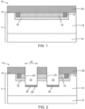
FIGS. 1-6 are cross-sectional views of a structure at successive fabrication stages of a processing method in accordance with embodiments of the invention. -
FIGS. 7-8 are cross-sectional views of a structure at successive fabrication stages of a processing method in accordance with alternative embodiments of the invention. -
FIGS. 9-11 are cross-sectional views of a structure at successive fabrication stages of a processing method in accordance with alternative embodiments of the invention. - With reference to
FIG. 1 and in accordance with embodiments of the invention, astructure 10 for a field-effect transistor may be formed using asemiconductor substrate 11 that includes abulk substrate 12 and asemiconductor layer 14 formed by, for example, epitaxial growth on thebulk substrate 12. In an embodiment, thesemiconductor layer 14 of thesemiconductor substrate 11 may be comprised of a wide bandgap semiconductor material, such as silicon carbide. In an embodiment, thebulk substrate 12 of thesemiconductor substrate 11 may be comprised of a wide bandgap semiconductor material. In an embodiment, thesemiconductor substrate 11 may be comprised of silicon carbide, which is a wide bandgap semiconductor material. In an embodiment, thesemiconductor substrate 11 may be comprised of diamond, which is a wide bandgap semiconductor material. In an embodiment, thebulk substrate 12 and thesemiconductor layer 14 may be comprised of a semiconductor material having a melting point greater than the melting point of silicon. In an embodiment, thebulk substrate 12 and thesemiconductor layer 14 may be comprised of silicon carbide that is doped to have n-type electrical conductivity. In an embodiment, thebulk substrate 12 and thesemiconductor layer 14 may be comprised of silicon carbide that is doped to have n-type electrical conductivity with thebulk substrate 12 having a higher dopant concentration and a lower electrical resistivity than thesemiconductor layer 14. In an embodiment, thebulk substrate 12 may have a resistivity of less than 25 mOhm-cm. In an embodiment, thesemiconductor layer 14 may include a buffer sublayer grown directly on thebulk substrate 12 and a drift sublayer grown on the buffer sublayer, and the drift sublayer may have a dopant concentration and a thickness that are optimized for device operation in a 650 volt to 1200 volt range. In an embodiment, thebulk substrate 12 may operate as the drain of the field-effect transistor. - A
doped region 16 may be formed in thesemiconductor layer 14 adjacent to atop surface 13 of thesemiconductor substrate 11. Thedoped region 16 is doped to have an opposite conductivity type from thesemiconductor layer 14. Thedoped region 16 has a lower boundary that defines an interface with the underlying semiconductor material of thesemiconductor layer 14 across which the dopant type changes. In an embodiment, thedoped region 16 may define a body of the field-effect transistor. - The
doped region 16 may be formed by introducing a dopant of a given conductivity type by, for example, ion implantation into thesemiconductor layer 14. An implantation mask may be formed to define a selected area on atop surface 13 of thesemiconductor substrate 11 that is exposed for the implantation of ions. The implantation mask may include a hardmask that is applied and patterned to form an opening exposing the selected area on thetop surface 13 and determining, at least in part, the location and horizontal dimensions of thedoped region 16. The implantation conditions (e.g., ion species, dose, kinetic energy, substrate temperature) may be selected to tune the electrical and physical characteristics of thedoped region 16, to minimize defects, and to maximize the ionization and activation of the implanted dopants. In an embodiment, the ion implantation may be performed at substrate temperature in a range of 200°C to 600°C to minimize defect formation. The implantation mask, which is compatible with the implantation conditions and is stripped following implantation, has a thickness and stopping power sufficient to block the implantation of ions in masked areas. In an embodiment, thedoped region 16 may be doped with a concentration of a p-type dopant (e.g., aluminum) to provide p-type electrical conductivity. -
Contacts 19 may be formed at the periphery of thedoped region 16. Thecontacts 19 may be formed by ion implantation using an implantation mask, and thecontacts 19 may have the same conductivity type (e.g., p-type) as the dopedregion 16 but at a higher dopant concentration. Thecontacts 19 may provide body contacts to the body of the field-effect transistor defined by the dopedregion 16. - A doped
region 18 may be formed in thesemiconductor layer 14 adjacent to atop surface 13 of thesemiconductor substrate 11. The dopedregion 18 has the same conductivity type as thesemiconductor layer 14 but at a higher dopant concentration. The dopedregion 18 has an upper boundary that may be coplanar or substantially coplanar with thetop surface 13 of thesemiconductor substrate 11 and a lower boundary that defines an interface with the dopedregion 16 across which the conductivity type changes. In an embodiment, the dopedregion 18 may define a source of the field-effect transistor. - The doped
region 18 may be formed by introducing a dopant of a given conductivity type by, for example, ion implantation into thesemiconductor layer 14. An implantation mask may be formed to define a selected area on atop surface 13 of thesemiconductor substrate 11 that is exposed for the implantation of ions. The implantation mask may include a hardmask that is applied and patterned to form an opening exposing the selected area on thetop surface 13 of thesemiconductor substrate 11 and determining, at least in part, the location and horizontal dimensions of the dopedregion 18. The implantation conditions (e.g., ion species, dose, kinetic energy, substrate temperature) may be selected to tune the electrical and physical characteristics of the dopedregion 18. In an embodiment, the ion implantation may be performed at substrate temperature in a range of 200°C to 600°C to minimize defect formation. The implantation mask, which is compatible with the implantation conditions and is stripped following implantation, has a thickness and stopping power sufficient to block the implantation of ions in masked areas. In an embodiment, the dopedregion 18 may be doped with a concentration of an n-type dopant (e.g., nitrogen and/or phosphorus) to provide n-type electrical conductivity. In an embodiment, the dopedregion 18 may be doped with a higher concentration of the n-type dopant than thesemiconductor layer 14. - A
hardmask 20 is applied on thetop surface 13 of thesemiconductor substrate 11 and, in particular, thehardmask 20 may be disposed on thetop surface 13 over the dopedregions hardmask 20 may be comprised of a material that is characterized by a high melting point. In an embodiment, thehardmask 20 may be comprised of a material that is characterized by a melting point greater than or equal to 2000°C. In an embodiment, thehardmask 20 may be comprised of a material that is an electrical insulator and that is characterized by a melting point greater than or equal to 2000°C. In an embodiment, thehardmask 20 may be comprised of a material that is an insulating ceramic having a melting point greater than or equal to 2000°C. In an embodiment, thehardmask 20 may be comprised of a material that is a high-resistivity semiconductor material having a melting point greater than or equal to 2000°C. In an embodiment, thehardmask 20 may be comprised of a material characterized by a coefficient of thermal expansion that is similar to the coefficient of thermal expansion of crystalline silicon carbide. - In embodiments, the
hardmask 20 may include one or more layers each comprised of a material that is characterized by a melting point greater than or equal to 2000°C. In an embodiment, thehardmask 20 may include a layer comprised of aluminum nitride. In an embodiment, thehardmask 20 may include a layer comprised of polycrystalline silicon carbide. In an embodiment, thehardmask 20 may include a layer comprised of either aluminum nitride or polycrystalline silicon carbide that is disposed on a layer comprised of aluminum oxide. In an embodiment, thehardmask 20 may include a layer comprised of polycrystalline silicon carbide that is disposed on a layer comprised of aluminum nitride. - With reference to
FIG. 2 in which like reference numerals refer to like features inFIG. 1 and at a subsequent fabrication stage,trenches 22 are formed by lithography and etching processes that extend through thehardmask 20 into thesemiconductor substrate 11. More specifically, eachtrench 22 includes an upper portion that extends through thehardmask 20 and a lower portion that extends from thetop surface 13 of thesemiconductor substrate 11 through both of the dopedregions semiconductor layer 14 beneath the dopedregion 16. Eachtrench 22, which may have a width dimension W, has asidewall 24 and a trench bottom 26 that is positioned between thetop surface 13 and the interface between thebulk substrate 12 and thesemiconductor layer 14. In contrast to conventional process flows, thehardmask 20 is not removed from thetop surface 13 after thetrenches 22 are formed. - A doped
region 28 may be formed in thesemiconductor layer 14 beneath thetrench bottom 26 of each of thetrenches 22. The dopedregions 28 are positioned in a vertical direction between thetrenches 22 and thebulk substrate 12 operating as the drain of the field-effect transistor. The dopedregions 28 have an opposite conductivity type from thesemiconductor layer 14 and the dopedregion 16. The dopedregions 28 may participate in defining a p-shield of the field-effect transistor. - The doped
regions 28 may be formed by introducing a dopant of a given conductivity type by, for example, ion implantation into thesemiconductor layer 14. Thetrenches 22 in thehardmask 20 may determine, at least in part, the location and horizontal dimensions of the dopedregions 28. Thehardmask 20 has a thickness and stopping power sufficient to block the implantation of ions in masked areas. The implantation conditions (e.g., ion species, dose, kinetic energy, substrate temperature) may be selected to tune the electrical and physical characteristics of the dopedregions 28. In an embodiment, the dopedregions 28 may be doped with a concentration of a p-type dopant (e.g., aluminum) to provide p-type electrical conductivity. - A high-temperature anneal may be performed following the implantations to activate the implanted dopants and to alleviate post-implantation crystal damage. The high-temperature anneal may be performed with a removable carbon capping layer applied as a temporary coating on the
hardmask 20 and at a high temperature, such as a temperature in a range of 1600°C to 1900°C. Thehardmask 20, which can withstand the high anneal temperature, is disposed on thetop surface 13 during the anneal and functions to enhance the surface protection during the anneal. The removable carbon capping layer may prevent silicon outgassing from surface areas, such as those surface areas inside thetrenches 22, that are not covered and protected by thehardmask 20 during the high-temperature anneal. The carbon capping layer, which may be comprised of burned photoresist or a deposited layer of carbon, is removed following the high-temperature anneal. In a conventional process flow, all hardmasks are removed before the high-temperature anneal. - With reference to
FIG. 3 in which like reference numerals refer to like features inFIG. 2 and at a subsequent fabrication stage, a gate structure including agate dielectric layer 32 and agate conductor layer 34 is formed inside each of thetrenches 22. In an embodiment, the gate conductor layers 34 may be comprised of polysilicon that is heavily doped with an n-type dopant, such as phosphorus or arsenic, and the gate dielectric layers 32 may be comprised of a dielectric material, such as silicon dioxide, that is an electrical insulator. The gate dielectric layers 32 and gate conductor layers 34 may be deposited and then etched back using either reactive ion etching or chemical mechanical polishing such that eachgate conductor layer 34 has atop surface 36 that is coplanar or substantially coplanar with atop surface 21 of thehardmask 20. Eachgate conductor layer 34 extends through thehardmask 20 and the dopedregions semiconductor substrate 11. Thehardmask 20, which is present on thetop surface 13, assists with self-alignment during the formation of the gate structures in thetrenches 22. Thegate dielectric layer 32 andgate conductor layer 34 of each gate structure project in a vertical direction above thetop surface 13 due to the existence of the upper portions of thetrenches 22 in thehardmask 20. - With reference to
FIG. 4 in which like reference numerals refer to like features inFIG. 3 and at a subsequent fabrication stage, thegate dielectric layer 32 and thegate conductor layer 34 may be recessed by an etching process such that thetop surface 36 of eachgate conductor layer 34 is disposed within thetrenches 22 below thetop surface 21 of thehardmask 20. In an embodiment, thetop surface 36 of eachgate conductor layer 34 may be disposed in a vertical direction between thetop surface 21 of thehardmask 20 and thetop surface 13 of thesemiconductor substrate 11. Eachgate conductor layer 34 has an upper portion disposed above thetop surface 13 of thesemiconductor substrate 11 and a lower portion disposed in one of thetrenches 22 below thetop surface 13 of thesemiconductor substrate 11. The upper and lower portions of eachgate conductor layer 34 are disposed on opposite sides of thetop surface 13 of thesemiconductor substrate 11. - With reference to
FIG. 5 in which like reference numerals refer to like features inFIG. 4 and at a subsequent fabrication stage,dielectric layers 38 are formed in the open spaces inside thetrenches 22 over the recessed gate conductor layers 34. The dielectric layers 38 may be comprised of a dielectric material, such as silicon dioxide, that is an electrical insulator. In an embodiment, thedielectric layers 38 may be formed by depositing a dielectric material and polishing the dielectric material by chemical mechanical polishing to be coplanar or substantially coplanar with thetop surface 21 of thehardmask 20. In an alternative embodiment, the formation of thedielectric layers 38 may include oxidizing the material of the gate conductor layers 34 by an oxidation process and polishing the oxidized material. The oxidation temperature may be selected in order to maximize the oxidation of the material constituting the gate conductor layers 34 and to minimize the oxidation of surrounding materials, such as the material of thehardmask 20. - The dielectric layers 38 may have a
top surface 39 that is coplanar or substantially coplanar with thetop surface 21 of thehardmask 20. Due to the spatial constraint imposed by the upper portions of thetrenches 22 in thehardmask 20, thedielectric layers 38 may have a width dimension that is equal or substantially equal to the width dimension W of thetrenches 22. The formation of thedielectric layers 38 inside the upper portions of thetrenches 22 may enable an increase in the thickness of the dielectric layers 38. - With reference to
FIG. 6 in which like reference numerals refer to like features inFIG. 5 and at a subsequent fabrication stage, thehardmask 20 may be removed from thetop surface 13 by an etching process. The removal of thehardmask 20 reveals thetop surface 13 of thesemiconductor substrate 11 and provides access for contacting the dopedregions hardmask 20 may be removed without disturbing thedielectric layers 38, which are also revealed when thehardmask 20 is removed. -
Dielectric spacers 40 may be formed on the sidewalls of the dielectric layers 38. In an embodiment, thedielectric spacers 40 may be comprised of a dielectric material, such as silicon nitride, silicon oxynitride, or silicon dioxide, that is an electrical insulator and that is conformally deposited and then anisotropically etched. In an alternative embodiment, thedielectric spacers 40 may be omitted from thestructure 10. - Middle-of-line processing and back-end-of-line processing may follow, which includes formation of silicide, contacts, vias, and wiring for an interconnect structure that is coupled to the
structure 10. In an embodiment, the completedstructure 10 may be used to form a metal-oxide-semiconductor field-effect transistor. - With reference to
FIG. 7 and in accordance with alternative embodiments, thehardmask 20 may be removed after the gate conductor layers 34 are formed and without recessing the gate conductor layers 34 before the removal of thehardmask 20. The upper portion of eachgate conductor layer 34 is disposed above thetop surface 13 of thesemiconductor substrate 11 and is no longer surrounded by thehardmask 20. - With reference to
FIG. 8 in which like reference numerals refer to like features inFIG. 7 and at a subsequent fabrication stage, thedielectric layers 38 may be formed on the upper portions of the gate conductor layers 34 after removing thehardmask 20. In an embodiment, thedielectric layers 38 may be formed by an oxidation process, which effectively shortens the height of eachgate conductor layer 34. - With reference to
FIG. 9 and in accordance with alternative embodiments, asilicide layer 42 may be formed by a silicidation process on eachgate conductor layer 34. Thetrenches 22 in thehardmask 20 enable the silicide layers 42 to be formed with self-alignment to the gate conductor layers 34. Due to the spatial constraint imposed by thetrenches 22, the silicide layers 42 may have a width dimension that is equal or approximately equal to the width dimension W of thetrenches 22. In an embodiment, the silicide layers 42 may be disposed below thetop surface 21 of thehardmask 20. - In an embodiment, the silicide layers 42 may be formed by depositing a silicide-forming metal, performing one or more annealing steps to form a silicide phase by reacting the silicide-forming metal with the semiconductor material of the gate conductor layers 34, and selectively removing any unreacted silicide-forming metal. The silicide layers 42 may then be subjected to an additional annealing step at a higher temperature to form a lower-resistance silicide phase. In an embodiment, the silicide-forming metal employed to form the silicide layers 42 may be comprised of nickel.
- With reference to
FIG. 10 in which like reference numerals refer to like features inFIG. 9 and at a subsequent fabrication stage, thedielectric layers 38 may be formed on the upper portions of the gate conductor layers 34 after forming the silicide layers 42. In an embodiment, thedielectric layers 38 may be deposited and planarized to fill the spaces inside thetrenches 22 over the silicide layers 42. - With reference to
FIG. 11 in which like reference numerals refer to like features inFIG. 10 and at a subsequent fabrication stage, thehardmask 20 may be removed by an etching process after forming thedielectric layers 38, followed by the optional formation of thedielectric spacers 40. Thehardmask 20 may be removed without disturbing the dielectric layers 38. - The methods as described above are used in the fabrication of integrated circuit chips. The resulting integrated circuit chips can be distributed by the fabricator in raw wafer form (e.g., as a single wafer that has multiple unpackaged chips), as a bare die, or in a packaged form. The chip may be integrated with other chips, discrete circuit elements, and/or other signal processing devices as part of either an intermediate product or an end product. The end product can be any product that includes integrated circuit chips, such as computer products having a central processor or smartphones.
- References herein to terms modified by language of approximation, such as "about", "approximately", and "substantially", are not to be limited to the precise value specified. The language of approximation may correspond to the precision of an instrument used to measure the value and, unless otherwise dependent on the precision of the instrument, may indicate a range of +/- 10% of the stated value(s).
- References herein to terms such as "vertical", "horizontal", etc. are made by way of example, and not by way of limitation, to establish a frame of reference. The term "horizontal" as used herein is defined as a plane parallel to a conventional plane of a semiconductor substrate, regardless of its actual three-dimensional spatial orientation. The terms "vertical" and "normal" refer to a direction in the frame of reference perpendicular to the horizontal, as just defined. The term "lateral" refers to a direction in the frame of reference within the horizontal plane.
- A feature "connected" or "coupled" to or with another feature may be directly connected or coupled to or with the other feature or, instead, one or more intervening features may be present. A feature may be "directly connected" or "directly coupled" to or with another feature if intervening features are absent. A feature may be "indirectly connected" or "indirectly coupled" to or with another feature if at least one intervening feature is present. A feature "on" or "contacting" another feature may be directly on or in direct contact with the other feature or, instead, one or more intervening features may be present. A feature may be "directly on" or in "direct contact" with another feature if intervening features are absent. A feature may be "indirectly on" or in "indirect contact" with another feature if at least one intervening feature is present. Different features "overlap" if a feature extends over, and covers a part of, another feature.
- The descriptions of the various embodiments of the present invention have been presented for purposes of illustration but are not intended to be exhaustive or limited to the embodiments disclosed. Many modifications and variations will be apparent to those of ordinary skill in the art without departing from the scope and spirit of the described embodiments. The terminology used herein was chosen to best explain the principles of the embodiments, the practical application or technical improvement over technologies found in the marketplace, or to enable others of ordinary skill in the art to understand the embodiments disclosed herein.
Claims (15)
- A structure for a field-effect transistor, the structure comprising:a semiconductor substrate including a top surface, a doped region adjacent to the top surface, and a trench that extends through the doped region, the semiconductor substrate comprising a wide bandgap semiconductor material; anda gate structure including a gate conductor layer, the gate conductor layer having a first portion disposed above the top surface of the semiconductor substrate and a second portion disposed inside the trench below the top surface of the semiconductor substrate.
- The structure of claim 1 wherein the gate structure further includes a silicide layer on the first portion of the gate conductor layer.
- The structure of claim 2 wherein the silicide layer and the trench have substantially equal width dimensions.
- The structure of one of claims 1 to 3 further comprising:a dielectric layer on the first portion of the gate conductor layer,wherein the dielectric layer and the trench have substantially equal width dimensions.
- The structure of claim 4 further comprising:
a dielectric spacer on the dielectric layer. - The structure of one of claims 1 to 5 wherein the gate conductor layer extends through the doped region, and/or wherein the wide bandgap semiconductor material comprises silicon carbide.
- A method of forming a structure for a field-effect transistor, the method comprising:forming a doped region in a semiconductor substrate adjacent to a top surface of the semiconductor substrate, wherein the semiconductor substrate comprises a wide bandgap semiconductor material;forming a trench in the semiconductor substrate, wherein the trench extends through the doped region; andforming a gate structure including a gate conductor layer, wherein the gate conductor layer has a first portion disposed above the top surface of the semiconductor substrate and a second portion disposed inside the trench below the top surface of the semiconductor substrate.
- The method of claim 7 wherein forming the trench in the semiconductor substrate comprises:forming a hardmask on the top surface of the semiconductor substrate,wherein the trench extends through the hardmask into the semiconductor substrate.
- The method of claim 8 further comprising:forming a silicide layer on the first portion of the gate conductor layer; andremoving the hardmask after forming the silicide layer.
- The method of claim 8 further comprising:
recessing the gate conductor layer relative to a top surface of the hardmask, wherein the gate conductor layer has a top surface disposed between the top surface of the hardmask and the top surface of the semiconductor substrate. - The method of claim 10 further comprising:forming a silicide layer on the gate conductor layer;forming a dielectric layer inside a portion of the trench over the silicide layer and the gate conductor layer; andremoving the hardmask after forming the silicide layer and the dielectric layer.
- The method of claim 10 further comprising:
forming a dielectric layer inside a portion of the trench over the gate conductor layer. - The method of one of claims 8 to 12 wherein the hardmask comprises a material having a melting point that is greater than or equal to 2000°C, or wherein the hardmask comprises aluminum nitride, or wherein the hardmask comprises polycrystalline silicon carbide.
- The method of one of claims 8 to 12 wherein the hardmask includes a first layer and a second layer that is disposed on the first layer, the first layer comprises aluminum oxide, and the second layer comprises aluminum nitride or polycrystalline silicon carbide, or the first layer comprises aluminum nitride, and the second layer comprises polycrystalline silicon carbide.
- The method of claims 8, 13 and 14 further comprising:removing the hardmask after forming the gate structure; andforming a dielectric layer by an oxidation process on the gate conductor layer after removing the hardmask.
Applications Claiming Priority (1)
| Application Number | Priority Date | Filing Date | Title |
|---|---|---|---|
| US18/098,999 US20240250126A1 (en) | 2023-01-19 | 2023-01-19 | Field-effect transistors formed using a wide bandgap semiconductor material |
Publications (1)
| Publication Number | Publication Date |
|---|---|
| EP4404270A1 true EP4404270A1 (en) | 2024-07-24 |
Family
ID=88510862
Family Applications (1)
| Application Number | Title | Priority Date | Filing Date |
|---|---|---|---|
| EP23205075.7A Pending EP4404270A1 (en) | 2023-01-19 | 2023-10-23 | Field-effect transistors formed using a wide bandgap semiconductor material |
Country Status (3)
| Country | Link |
|---|---|
| US (1) | US20240250126A1 (en) |
| EP (1) | EP4404270A1 (en) |
| CN (1) | CN118367022A (en) |
Citations (4)
| Publication number | Priority date | Publication date | Assignee | Title |
|---|---|---|---|---|
| US20040124461A1 (en) * | 2001-07-24 | 2004-07-01 | Gajda Mark A. | Trench-gate semiconductor devices, and their manufacture |
| US20140170823A1 (en) * | 2012-12-13 | 2014-06-19 | Anpec Electronics Corporation | Method for fabricating trench type transistor |
| US20180197947A1 (en) * | 2015-10-16 | 2018-07-12 | Fuji Electric Co., Ltd. | Semiconductor device and method of manufacturing semiconductor device |
| WO2018212282A1 (en) * | 2017-05-17 | 2018-11-22 | ローム株式会社 | Semiconductor device |
Family Cites Families (8)
| Publication number | Priority date | Publication date | Assignee | Title |
|---|---|---|---|---|
| US5641695A (en) * | 1995-10-02 | 1997-06-24 | Motorola | Method of forming a silicon carbide JFET |
| US20060197148A1 (en) * | 2005-02-04 | 2006-09-07 | Hsu Hsiu-Wen | Trench power moset and method for fabricating the same |
| JP2006339476A (en) * | 2005-06-03 | 2006-12-14 | Elpida Memory Inc | Semiconductor device and manufacturing method thereof |
| JP6335089B2 (en) * | 2014-10-03 | 2018-05-30 | ルネサスエレクトロニクス株式会社 | Manufacturing method of semiconductor device |
| JP2016162918A (en) * | 2015-03-03 | 2016-09-05 | トヨタ自動車株式会社 | Semiconductor device manufacturing method |
| US9852923B2 (en) * | 2015-04-02 | 2017-12-26 | Applied Materials, Inc. | Mask etch for patterning |
| US10833150B2 (en) * | 2018-07-11 | 2020-11-10 | International Business Machines Corporation | Fast recrystallization of hafnium or zirconium based oxides in insulator-metal structures |
| JP7755242B2 (en) * | 2022-02-07 | 2025-10-16 | 富士電機株式会社 | Silicon carbide semiconductor device and method for manufacturing silicon carbide semiconductor device |
-
2023
- 2023-01-19 US US18/098,999 patent/US20240250126A1/en active Pending
- 2023-10-23 EP EP23205075.7A patent/EP4404270A1/en active Pending
- 2023-10-31 CN CN202311430851.5A patent/CN118367022A/en active Pending
Patent Citations (4)
| Publication number | Priority date | Publication date | Assignee | Title |
|---|---|---|---|---|
| US20040124461A1 (en) * | 2001-07-24 | 2004-07-01 | Gajda Mark A. | Trench-gate semiconductor devices, and their manufacture |
| US20140170823A1 (en) * | 2012-12-13 | 2014-06-19 | Anpec Electronics Corporation | Method for fabricating trench type transistor |
| US20180197947A1 (en) * | 2015-10-16 | 2018-07-12 | Fuji Electric Co., Ltd. | Semiconductor device and method of manufacturing semiconductor device |
| WO2018212282A1 (en) * | 2017-05-17 | 2018-11-22 | ローム株式会社 | Semiconductor device |
Also Published As
| Publication number | Publication date |
|---|---|
| CN118367022A (en) | 2024-07-19 |
| US20240250126A1 (en) | 2024-07-25 |
Similar Documents
| Publication | Publication Date | Title |
|---|---|---|
| US6060746A (en) | Power transistor having vertical FETs and method for making same | |
| US6413829B1 (en) | Field effect transistor in SOI technology with schottky-contact extensions | |
| US9018739B2 (en) | Semiconductor device and method of fabricating the same | |
| US10522644B1 (en) | Different upper and lower spacers for contact | |
| US20180366372A1 (en) | Integrated circuit structure with stepped epitaxial region | |
| US9478615B2 (en) | Blanket short channel roll-up implant with non-angled long channel compensating implant through patterned opening | |
| US10741451B2 (en) | FinFET having insulating layers between gate and source/drain contacts | |
| JP2004336049A (en) | Structure and manufacturing method of notch type gate field effect transistor | |
| EP4421872A1 (en) | Semiconductor structure with device including at least one in-well porous region | |
| US12446270B2 (en) | Junction field-effect transistors implemented in a wide bandgap semiconductor material | |
| US7993989B2 (en) | Vertical spacer forming and related transistor | |
| US11239315B2 (en) | Dual trench isolation structures | |
| US20240274712A1 (en) | Field-effect transistors with self-aligned p-shield contacts | |
| US20240250126A1 (en) | Field-effect transistors formed using a wide bandgap semiconductor material | |
| US6326273B1 (en) | Method of fabricating a field effect transistor with trapezoidal shaped gate dielectric and/or gate electrode | |
| US6436773B1 (en) | Fabrication of test field effect transistor structure | |
| US12520523B2 (en) | Field-effect transistors with a high-temperature hardmask and self-aligned p-shield | |
| EP4421878A1 (en) | Field-effect transistors with deposited gate dielectric layers | |
| US20250063748A1 (en) | Insulating-gate bipolar transistors including a reverse conducting diode | |
| US20260068279A1 (en) | Extended drain metal oxide semiconductor device | |
| US20240355872A1 (en) | Transistors with field-shield contacts and base contacts | |
| US20260129939A1 (en) | Ldmos transistor with split gate field plate tapered toward drain region and related method | |
| US20240395932A1 (en) | Wraparound gate structure | |
| US12324217B2 (en) | Laterally diffused metal-oxide semiconductor with gate contact | |
| US20260123005A1 (en) | Transistor with field plate |
Legal Events
| Date | Code | Title | Description |
|---|---|---|---|
| PUAI | Public reference made under article 153(3) epc to a published international application that has entered the european phase |
Free format text: ORIGINAL CODE: 0009012 |
|
| STAA | Information on the status of an ep patent application or granted ep patent |
Free format text: STATUS: THE APPLICATION HAS BEEN PUBLISHED |
|
| AK | Designated contracting states |
Kind code of ref document: A1 Designated state(s): AL AT BE BG CH CY CZ DE DK EE ES FI FR GB GR HR HU IE IS IT LI LT LU LV MC ME MK MT NL NO PL PT RO RS SE SI SK SM TR |
|
| STAA | Information on the status of an ep patent application or granted ep patent |
Free format text: STATUS: REQUEST FOR EXAMINATION WAS MADE |
|
| 17P | Request for examination filed |
Effective date: 20241104 |
|
| RBV | Designated contracting states (corrected) |
Designated state(s): AL AT BE BG CH CY CZ DE DK EE ES FI FR GB GR HR HU IE IS IT LI LT LU LV MC ME MK MT NL NO PL PT RO RS SE SI SK SM TR |