EP4404269A1 - Semiconductor device including porous semiconductor material adjacent an isolation structure - Google Patents
Semiconductor device including porous semiconductor material adjacent an isolation structure Download PDFInfo
- Publication number
- EP4404269A1 EP4404269A1 EP23192844.1A EP23192844A EP4404269A1 EP 4404269 A1 EP4404269 A1 EP 4404269A1 EP 23192844 A EP23192844 A EP 23192844A EP 4404269 A1 EP4404269 A1 EP 4404269A1
- Authority
- EP
- European Patent Office
- Prior art keywords
- region
- well region
- isolation structure
- porous
- well
- Prior art date
- Legal status (The legal status is an assumption and is not a legal conclusion. Google has not performed a legal analysis and makes no representation as to the accuracy of the status listed.)
- Pending
Links
Images




Classifications
-
- H—ELECTRICITY
- H10—SEMICONDUCTOR DEVICES; ELECTRIC SOLID-STATE DEVICES NOT OTHERWISE PROVIDED FOR
- H10D—INORGANIC ELECTRIC SEMICONDUCTOR DEVICES
- H10D62/00—Semiconductor bodies, or regions thereof, of devices having potential barriers
- H10D62/10—Shapes, relative sizes or dispositions of the regions of the semiconductor bodies; Shapes of the semiconductor bodies
- H10D62/113—Isolations within a component, i.e. internal isolations
-
- H—ELECTRICITY
- H10—SEMICONDUCTOR DEVICES; ELECTRIC SOLID-STATE DEVICES NOT OTHERWISE PROVIDED FOR
- H10D—INORGANIC ELECTRIC SEMICONDUCTOR DEVICES
- H10D30/00—Field-effect transistors [FET]
- H10D30/01—Manufacture or treatment
- H10D30/021—Manufacture or treatment of FETs having insulated gates [IGFET]
- H10D30/0221—Manufacture or treatment of FETs having insulated gates [IGFET] having asymmetry in the channel direction, e.g. lateral high-voltage MISFETs having drain offset region or extended-drain MOSFETs [EDMOS]
-
- H—ELECTRICITY
- H10—SEMICONDUCTOR DEVICES; ELECTRIC SOLID-STATE DEVICES NOT OTHERWISE PROVIDED FOR
- H10D—INORGANIC ELECTRIC SEMICONDUCTOR DEVICES
- H10D30/00—Field-effect transistors [FET]
- H10D30/01—Manufacture or treatment
- H10D30/021—Manufacture or treatment of FETs having insulated gates [IGFET]
- H10D30/028—Manufacture or treatment of FETs having insulated gates [IGFET] of double-diffused metal oxide semiconductor [DMOS] FETs
- H10D30/0281—Manufacture or treatment of FETs having insulated gates [IGFET] of double-diffused metal oxide semiconductor [DMOS] FETs of lateral DMOS [LDMOS] FETs
-
- H—ELECTRICITY
- H10—SEMICONDUCTOR DEVICES; ELECTRIC SOLID-STATE DEVICES NOT OTHERWISE PROVIDED FOR
- H10D—INORGANIC ELECTRIC SEMICONDUCTOR DEVICES
- H10D30/00—Field-effect transistors [FET]
- H10D30/60—Insulated-gate field-effect transistors [IGFET]
- H10D30/601—Insulated-gate field-effect transistors [IGFET] having lightly-doped drain or source extensions, e.g. LDD IGFETs or DDD IGFETs
- H10D30/603—Insulated-gate field-effect transistors [IGFET] having lightly-doped drain or source extensions, e.g. LDD IGFETs or DDD IGFETs having asymmetry in the channel direction, e.g. lateral high-voltage MISFETs having drain offset region or extended drain IGFETs [EDMOS]
-
- H—ELECTRICITY
- H10—SEMICONDUCTOR DEVICES; ELECTRIC SOLID-STATE DEVICES NOT OTHERWISE PROVIDED FOR
- H10D—INORGANIC ELECTRIC SEMICONDUCTOR DEVICES
- H10D30/00—Field-effect transistors [FET]
- H10D30/60—Insulated-gate field-effect transistors [IGFET]
- H10D30/64—Double-diffused metal-oxide semiconductor [DMOS] FETs
- H10D30/65—Lateral DMOS [LDMOS] FETs
-
- H—ELECTRICITY
- H10—SEMICONDUCTOR DEVICES; ELECTRIC SOLID-STATE DEVICES NOT OTHERWISE PROVIDED FOR
- H10D—INORGANIC ELECTRIC SEMICONDUCTOR DEVICES
- H10D62/00—Semiconductor bodies, or regions thereof, of devices having potential barriers
- H10D62/10—Shapes, relative sizes or dispositions of the regions of the semiconductor bodies; Shapes of the semiconductor bodies
- H10D62/113—Isolations within a component, i.e. internal isolations
- H10D62/115—Dielectric isolations, e.g. air gaps
- H10D62/116—Dielectric isolations, e.g. air gaps adjoining the input or output regions of field-effect devices, e.g. adjoining source or drain regions
-
- H—ELECTRICITY
- H10—SEMICONDUCTOR DEVICES; ELECTRIC SOLID-STATE DEVICES NOT OTHERWISE PROVIDED FOR
- H10D—INORGANIC ELECTRIC SEMICONDUCTOR DEVICES
- H10D62/00—Semiconductor bodies, or regions thereof, of devices having potential barriers
- H10D62/10—Shapes, relative sizes or dispositions of the regions of the semiconductor bodies; Shapes of the semiconductor bodies
- H10D62/117—Shapes of semiconductor bodies
-
- H—ELECTRICITY
- H10—SEMICONDUCTOR DEVICES; ELECTRIC SOLID-STATE DEVICES NOT OTHERWISE PROVIDED FOR
- H10D—INORGANIC ELECTRIC SEMICONDUCTOR DEVICES
- H10D62/00—Semiconductor bodies, or regions thereof, of devices having potential barriers
- H10D62/10—Shapes, relative sizes or dispositions of the regions of the semiconductor bodies; Shapes of the semiconductor bodies
- H10D62/13—Semiconductor regions connected to electrodes carrying current to be rectified, amplified or switched, e.g. source or drain regions
- H10D62/149—Source or drain regions of field-effect devices
- H10D62/151—Source or drain regions of field-effect devices of IGFETs
-
- H—ELECTRICITY
- H10—SEMICONDUCTOR DEVICES; ELECTRIC SOLID-STATE DEVICES NOT OTHERWISE PROVIDED FOR
- H10P—GENERIC PROCESSES OR APPARATUS FOR THE MANUFACTURE OR TREATMENT OF DEVICES COVERED BY CLASS H10
- H10P14/00—Formation of materials, e.g. in the shape of layers or pillars
- H10P14/60—Formation of materials, e.g. in the shape of layers or pillars of insulating materials
- H10P14/66—Formation of materials, e.g. in the shape of layers or pillars of insulating materials characterised by the type of materials
- H10P14/665—Porous materials
-
- H—ELECTRICITY
- H10—SEMICONDUCTOR DEVICES; ELECTRIC SOLID-STATE DEVICES NOT OTHERWISE PROVIDED FOR
- H10P—GENERIC PROCESSES OR APPARATUS FOR THE MANUFACTURE OR TREATMENT OF DEVICES COVERED BY CLASS H10
- H10P50/00—Etching of wafers, substrates or parts of devices
- H10P50/20—Dry etching; Plasma etching; Reactive-ion etching
- H10P50/28—Dry etching; Plasma etching; Reactive-ion etching of insulating materials
- H10P50/282—Dry etching; Plasma etching; Reactive-ion etching of insulating materials of inorganic materials
- H10P50/283—Dry etching; Plasma etching; Reactive-ion etching of insulating materials of inorganic materials by chemical means
-
- H—ELECTRICITY
- H10—SEMICONDUCTOR DEVICES; ELECTRIC SOLID-STATE DEVICES NOT OTHERWISE PROVIDED FOR
- H10D—INORGANIC ELECTRIC SEMICONDUCTOR DEVICES
- H10D30/00—Field-effect transistors [FET]
- H10D30/60—Insulated-gate field-effect transistors [IGFET]
- H10D30/601—Insulated-gate field-effect transistors [IGFET] having lightly-doped drain or source extensions, e.g. LDD IGFETs or DDD IGFETs
-
- H—ELECTRICITY
- H10—SEMICONDUCTOR DEVICES; ELECTRIC SOLID-STATE DEVICES NOT OTHERWISE PROVIDED FOR
- H10D—INORGANIC ELECTRIC SEMICONDUCTOR DEVICES
- H10D62/00—Semiconductor bodies, or regions thereof, of devices having potential barriers
- H10D62/10—Shapes, relative sizes or dispositions of the regions of the semiconductor bodies; Shapes of the semiconductor bodies
- H10D62/17—Semiconductor regions connected to electrodes not carrying current to be rectified, amplified or switched, e.g. channel regions
- H10D62/213—Channel regions of field-effect devices
- H10D62/221—Channel regions of field-effect devices of FETs
- H10D62/235—Channel regions of field-effect devices of FETs of IGFETs
- H10D62/299—Channel regions of field-effect devices of FETs of IGFETs having lateral doping variations
- H10D62/307—Channel regions of field-effect devices of FETs of IGFETs having lateral doping variations the doping variations being parallel to the channel lengths
Definitions
- the present disclosure relates to semiconductor structures and, more particularly, to embodiments of a semiconductor structure including a semiconductor device and to embodiments of a method of forming the semiconductor structure.
- LDMOSFETs laterally diffused metal oxide semiconductor field effect transistors
- RF radio-frequency
- microwave power amplifiers etc.
- BVdss drain-to-source breakdown voltage
- Gm reduced transconductance
- BVdss refers to the specific drain-to-source voltage (Vds) that results in the transistor entering the breakdown region at which Vds is too high and the drain current (Id) spikes (i.e., increases dramatically).
- Gm refers to the ratio of the change in Id to the change in gate voltage (Vg) (i.e., Id2-Id1/Vg2-Vg1) over, for example, some period of time in the I/V curve for the device.
- the structure can include a semiconductor layer and a device.
- the device can include at least a first well region in the semiconductor layer, a porous region in the first well region, and an isolation structure in the first well region.
- the porous region can specifically be positioned immediately adjacent to at least one side of the isolation structure.
- Some embodiments of the structure disclosed herein can include a semiconductor layer and a device.
- the device can include a first well region in the semiconductor layer, a porous region in the first well region, and an isolation structure in the first well region. Again, the porous region can be positioned immediately adjacent to at least one side of the isolation structure.
- the device can further include a drain region immediately adjacent to the first well region.
- the device can further include a second well region in the semiconductor layer positioned laterally adjacent to the first well region.
- the porous region and the isolation structure can specifically be within the first well region between the second well region and the drain region.
- the device can further include a source region immediately adjacent to the second well region.
- the device can further include a gate on the semiconductor layer between the drain region and the source region.
- This gate can specifically be separated from the drain region by a first distance and from the source region by a second distance that is less than the first distance.
- the device can further include a drain drift region in the first well region bordering the isolation structure such that it is between the drain region and the gate.
- the method can include providing a semiconductor layer.
- the method can further include forming a device that includes a first well region in the semiconductor layer and, in the first well region, a porous region and an isolation structure.
- the porous region and the isolation structure can specifically be formed in the first well region such that the porous region is positioned immediately adjacent to at least one side of the isolation structure.
- LDMOSFETs are widely used in amplifiers, such as radio-frequency (RF) amplifiers, microwave power amplifiers, etc. because of their low on-resistance and because, in general, they have a relatively high blocking voltage (also referred to in the art as the drain-to-source breakdown voltage (BVdss)).
- RF radio-frequency
- BVdss drain-to-source breakdown voltage
- LDMOSFETs can exhibit performance degradation including, but not limited to, reduced BVdss and reduced transconductance (Gm).
- This semiconductor structure can include a semiconductor device with an active device region and, within the active device region, porous semiconductor material adjacent to an isolation structure.
- the porous semiconductor material can modify an electric field around the isolation structure and can thereby improve device performance.
- the semiconductor device can be an LDMOSFET.
- the LDMOSFET can include an active device region, a well region within the active device region and, within the well region, an isolation structure (e.g., a shallow trench isolation (STI) structure), a porous region immediately adjacent to the isolation structure.
- STI shallow trench isolation
- the porous region can, for example, be adjacent to opposing sides and a bottom of the STI structure, adjacent to one side and the bottom (but not the opposite side) of the STI structure, adjacent to the opposing sides only (but not the bottom) of the STI structure, or adjacent to one side only (but not the opposite side or the bottom) of the STI structure.
- a drain drift region of the LDMOSFET can be within the well region bordering the STI structure (e.g., extending between a channel region and a drain region). The presence of the porous region adjacent to the STI structure can modify the electric field within the drain drift and, as a result, can improve both BVdss and Gm of the device. Also disclosed herein are method embodiments for forming the semiconductor structure.
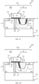
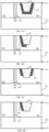
- FIGs. 1A-1D are cross-section diagrams illustrating disclosed embodiments of a semiconductor structure 100A-100D, respectively.
- Each of these semiconductor structures 100A-100D includes a semiconductor device 110A-110D with an active device region 130 and, within the active device region 130, porous semiconductor material (referred to herein as porous region 104) adjacent to an isolation structure.
- the porous semiconductor material can modify an electric field around the isolation structure 105 (e.g., an STI structure). and can thereby improve device performance.
- FIGs. 1A-1D disclosed herein are embodiments of a semiconductor structure 100A-100D.
- the semiconductor structure 100A-100D can include a semiconductor layer 101 having a first surface 191 (i.e., a bottom surface) and a second surface 192 (i.e., a top surface) opposite the first surface 191.
- the semiconductor layer 101 could be a bulk semiconductor substrate (e.g., a bulk silicon substrate or a bulk substrate of any other suitable semiconductor material, such as germanium, silicon germanium, etc.), as illustrated.
- a bulk semiconductor substrate e.g., a bulk silicon substrate or a bulk substrate of any other suitable semiconductor material, such as germanium, silicon germanium, etc.
- the semiconductor layer 101 could be the semiconductor layer (e.g., a silicon layer, a germanium layer, a silicon germanium layer, or a layer any other suitable semiconductor material) of a semiconductor-on-insulator structure (e.g., a silicon-on-insulator (SOI) structure) such that the first surface 191 is above and immediately adjacent to an insulator layer (not shown).
- the semiconductor layer 101 could be in either a bulk region or a semiconductor-on-insulator region (e.g., an SOI region) of a hybrid substrate (e.g., of a substrate, which is employed at an advanced SOI technology node, such as a fully-depleted SOI technology node, and which includes both bulk and SOI regions).
- the semiconductor layer 101 can, for example, be doped with a P-type dopant so as to have P-type conductivity at a relatively low conductivity level (e.g., so as to be a P- semiconductor layer). See the detailed discussion below regarding semiconductor material doping to achieve different conductivity types and levels.
- the semiconductor structure 100A-100D can further include a semiconductor device 110A-110D having an active device region 130 in the semiconductor layer 101.
- boundaries of the active device region 130 could, for example, be defined by shallow trench isolation (STI) structures external to the device. That is, external STI structures could extend into the semiconductor layer 101 from the second surface 192 so as to laterally surround and thereby define the boundaries of the device.
- STI shallow trench isolation
- the semiconductor device 110A-110D can be, for example, a LDMOSFET.
- the LDMOSFET 110A-110D can be an N-channel LDMOSFT.
- the LDMOSFET 110A-110D could be a P-channel LDMOSFET.
- the semiconductor device 110A-110D can include, within the semiconductor layer 101, a first well region 102 and a second well region 103 positioned laterally adjacent to the first well region 102.
- the first well region 102 and the second well region 103 can be physically separated by an additional region 108, as illustrated.
- the second well region 103 can abut the first well region 102 at a junction 107, as indicated by the dotted line.
- the first well region 102 and the second well region 103 can be doped regions (also referred to herein as dopant implant regions) within the semiconductor layer 101 and having different type conductivity.
- the conductivity type of the first and second well regions will vary depending upon whether the semiconductor device 110A-110D is an N-channel MOSFET or a P-channel MOSFET. Specifically, in the case of an N-channel MOSFET, the first well region 102 can be doped so as to have N-type conductivity and the second well region 103 can be doped so as to have P-type conductivity; whereas, in the case of a P-channel MOSFET, the first well region 102 can be doped so as to have P-type conductivity and the second well region 103 can be doped so as to have N-type conductivity.
- the additional region 108 can have the same type conductivity as the as the second well region 103 but at a lower conductivity level.
- the additional region 108 can be a P- region, which is continuous with the lower portion of the P- semiconductor layer 101.
- the first well region 102 i.e., a Pwell
- the second well region 103 i.e., an Nwell
- the first well region 102 and the second well region 103 can both be within a deep N- well (not shown) so as to be isolated from the lower portion of the P- semiconductor layer 101 and, thus, the additional region 108 could be an N- region.
- the semiconductor device 110A-110D can further include, within the first well region 102 in the semiconductor layer 101, a porous region 104 (i.e., a region of porous semiconductor material).
- a porous region 104 i.e., a region of porous semiconductor material.
- the porous region 104 can be a porous silicon (PS) region.
- the semiconductor layer 101 is a silicon germanium layer
- the porous region 104 can be a porous silicon germanium region, and so on.
- a porous region or a region of porous semiconductor material refers specifically to a region that includes nanopores within its microstructure.
- such nanopores can be introduced into a localized region of a semiconductor material through an electrochemical process.
- the porous region 104 can be contained within the first well region 102 extending, for example, from the second surface 192 of the semiconductor layer 101 to some depth above the bottom of the first well region 102 (i.e., the first well region 102 can extend deeper into the semiconductor layer 101 than the porous region 104, as illustrated).
- the semiconductor device 110A-110D can further include, within the first well region 102 in the semiconductor layer 101, an isolation structure 105 and, particularly, an internal STI structure.
- This STI structure 105 can include a trench that extends into the first well region 102 from the second surface 192 of the semiconductor layer 101.
- This STI structure 105 can further include one or more layers of isolation material (e.g., silicon dioxide, silicon nitride, etc.) filling the trench.
- This STI structure 105 can have opposing sides and a bottom and can be positioned within the first well region 102 so that portions of the first well region 102 surround the opposing sides and the bottom.
- the STI structure 105 and the porous region 104 (which as mentioned above is also within the first well region 102) can be positioned so that the porous region 104 is immediately adjacent to at least one of the opposing sides the STI structure 105.
- the relative positioning of the STI structure 105 and the porous region 104 within the first well region 102 can vary within the different semiconductor structure embodiments.
- the porous region 104 can extend deeper into the first well region 102 (as measured from the second surface 192) than the STI structure 105 and can also be positioned immediately adjacent to the opposing sides and the bottom surface of the STI structure 105. That is, the STI structure 105 can extend into the porous region 104 without going completely through it and can be narrower in width than the porous region 104. Thus, the STI structure 105 in the semiconductor device 110A is bordered by the porous region 104 at the bottom surface and at the opposing sides.
- the porous region 104 can extend deeper into the first well region 102 (as measured from the second surface 192) than the STI structure 105 and can be positioned immediately adjacent to one of the opposing sides and the bottom surface only of the STI structure 105. That is, the STI structure 105 can extend into one side of the porous region 104, without going completely through it.
- the STI structure 105 in the semiconductor device 110B is bordered by the porous region 104 on one side and at least along a portion of the bottom surface.
- the porous region 104 can extend shallower into the first well region 102 (as measured from the second surface 192) than the STI structure 105 and can be positioned immediately adjacent to the opposing sides only of the STI structure 105. That is, the STI structure 105 can extend into and completely through the porous region 104 and it can be narrower in width than the porous region 104. Thus, the STI structure 105 of the semiconductor device 110C is bordered by the porous region 104 on the opposing sides only.
- the porous region 104 can extend shallower into the first well region 102 (as measured from the second surface 192) than the STI structure 105 and it can be positioned immediately adjacent to one of the opposing sides only of the STI structure 105. That is, the STI structure 105 can extend into and completely through one side of the porous region 104. Thus, the STI structure 105 of the semiconductor device 110D is bordered by the porous region 104 on only one side.
- the semiconductor device 110A-110D can further include a drain region 112 and a source region 111.
- the drain region 112 and the source region 111 can have the same type conductivity as the first well region 102, but at a higher conductivity level.
- the drain region 112 and the source region 111 can be N+ drain and source regions; whereas, in the case of a P-channel LDMOSFET, the drain region 112 and the source region 111 can be P+ source and drain regions.
- the drain region 112 can be immediately adjacent to the first well region 102 distal to the additional region 108 (or junction 107) such that the porous region 104 and the STI structure 105 are between the second well region 103 and the drain region 112.
- the source region 111 can be immediately adjacent to the second well region 103 distal to the additional region 108 (or junction 107).
- Various different source/drain configurations for LDMOSFETs are well known in the art and, thus, the detail thereof have been omitted from this specification in order to allow the reader to focus on the salient aspects of the disclosed embodiments.
- the source/drain regions could have any suitable source/drain region configuration.
- they could be dopant implant regions, in situ doped epitaxial semiconductor material-filled or over-filled trenches, doped implant regions with raised source/drain regions (i.e., in situ doped epitaxial semiconductor layers) thereon, etc.
- the semiconductor device 110A-110D can further include a gate 115 on the second surface 192 of the semiconductor layer 101 between the drain region 112 and the source region 111.
- the gate 115 can be separated from the drain region 112 by a first distance (d1) and separated from the source region 111 by a second distance (d2) that is less than the d1.
- the gate 115 can be located on the portion of the second well region 103 between the source region 111 and the additional region 108 (or junction 107), can traverse the additional region 108 (or junction 107), and can further extend laterally over portions of the first well region 102 and the porous region 104 therein to or onto the STI structure 105.
- the gate 115 can include a gate dielectric layer 116 (including one or more layers of gate dielectric material) and a gate conductor layer 117 (including one or more layers of gate conductor material) on the gate dielectric layer 116.
- a gate dielectric layer 116 including one or more layers of gate dielectric material
- a gate conductor layer 117 including one or more layers of gate conductor material
- the gate could have any suitable LDMOSFET configuration.
- gate could be a gate first polysilicon gate, a gate first metal gate, a replacement metal gate, etc.
- the semiconductor device 110A-110D can further include gate sidewall spacers 118 (e.g., dielectric gate sidewalls spacers) positioned laterally adjacent to opposing sidewalls of the gate structure in order to electrically isolate the gate 115 from the adjacent source/drain regions.
- gate sidewall spacers 118 e.g., dielectric gate sidewalls spacers
- the semiconductor device 110A-110D can further include a channel region 120.
- the channel region 120 can be within the second well region 103 below the gate 115 and positioned laterally between the source region 111 and the drain region 112 and, more particularly, positioned laterally between the source region 111 and the junction 107 (or additional region 108).
- additional features of the semiconductor structure 100A-100D can include, but are not limited to, well contact region(s) (e.g., a well contact region, such as a dopant implant region, on the second well region 103 and having the same type conductivity), one or more layers of interlayer dielectric (ILD) material over the device, and middle of the line (MOL) contacts extending through the ILD material to the source region 111, drain region 112, gate 115 and well contact region(s).
- well contact region(s) e.g., a well contact region, such as a dopant implant region, on the second well region 103 and having the same type conductivity
- ILD interlayer dielectric
- MOL middle of the line
- the semiconductor device 110A-110D (e.g., LDMOSFET) includes a drain drift region 119 and, particularly, a current path in the first well region 102 between the gate 115 and the drain region 112 and bordering and, particularly, extending down and around the STI structure 105 including through the porous region 104.
- the presence of the porous region 104 within the conductive path in the drain drift region effectively modifies the electric field and, as a result, improves both BVdss and Gm of the device.
- the method can include providing a semiconductor layer 101 having a first surface 191 (i.e., a bottom surface) and a second surface 192 (i.e., a top surface) opposite the first surface 191 (see FIG. 2 ).
- the semiconductor layer 101 could be a bulk semiconductor substrate (e.g., a bulk silicon substrate or a bulk substrate of any other suitable semiconductor material, such as germanium, silicon germanium, etc.), as illustrated.
- the semiconductor layer 101 could be the semiconductor layer of a semiconductor-on-insulator structure.
- the semiconductor layer 101 could be in either a bulk region or a semiconductor-on-insulator region of a hybrid substrate.
- the semiconductor layer 101 can be doped with a P-type dopant so as to have P-type conductivity at a relatively low conductivity level (e.g., so as to be a P-semiconductor layer).
- the method can further include forming, within the semiconductor layer 101, a first well region 102 and a second well region 103 positioned laterally adjacent to the first well region 102 (e.g., see FIG. 2 ).
- the well regions can, for example, be formed by performing discrete dopant implantation processes. That is, a first mask could be formed on the second surface 192 of the semiconductor layer 101 and lithographically patterned and etched so as to have an opening that exposes a first area of the semiconductor layer. A dopant can be implanted through the opening to form the first well region with a desired conductivity type at a desired conductivity level. The first mask can then be removed.
- a second mask could be formed on the second surface 192 of the semiconductor layer 101 and lithographically patterned and etched so as to have an opening that exposes a second area of the semiconductor layer.
- a different dopant can be implanted through the opening to form the second well region with a desired conductivity type (which is different from that of the first well region) at a desired conductivity level.
- the second mask can then be removed.
- dopant implantation processes are well known in the art and, thus, the details thereof have been omitted from this specification in order to allow the reader to focus on the salient aspects of the disclosed embodiments.
- these two masked dopant implantation processes can be performed so that either the first well region 102 and the second well region 103 are physically separated by an additional region 108, as illustrated, or so that the second well region 103 abuts the first well region 102 at a junction 107, as indicated by the dotted line.
- the conductivity type of the first and second well regions will vary depending upon whether the semiconductor device 110A-110D is an N-channel MOSFET or a P-channel MOSFET.
- doping should be performed so that the first well region 102 has N-type conductivity and the second well region 103 has P-type conductivity; whereas, in the case of a P-channel MOSFET, doping should be performed so that the first well region 102 has P-type conductivity and the second well region 103 has N-type conductivity.
- a deep Nwell could be formed (not shown, using a similar masked dopant implantation process) and the first well region 102 (i.e., a Pwell) and the second well region 103 (i.e., an Nwell) could both be formed within the deep Nwell.
- the method can further include forming, within the first well region 102 in the semiconductor layer 101, a porous region 104 (i.e., a region of porous semiconductor material) (see FIGs. 3 and 4 ).
- a porous region 104 i.e., a region of porous semiconductor material
- yet another mask 301 could be formed on the second surface 192 of the semiconductor layer 101.
- This mask 301 could be lithographically patterned and etched to include an opening 302, which exposes a section of the second surface 192 above the first well region 102 and in a desired area for the porous region (see FIG. 3 ).
- Electrochemical processing can then be performed to form the porous region in the first well region of the semiconductor below the exposed surface. That is, this electrochemical processing converts the semiconductor material in the region of the semiconductor layer below the exposed surface to a porous semiconductor material by causing the formation of nanopores to be introduced into the region.
- an etchant 405 i.e., an etching solution, such as a hydrofluoric acid (HF) electrolyte solution
- a power source 401 can have a negative electrode 403 connected to the etchant 405 to supply electrons to the etchant 405 (i.e., the cathode) and a positive electrode 402 connected to the semiconductor layer 101 to remove electrons from the etchant 405 (i.e., the anode). Electrochemical reactions occur at both the cathode and the anode. At the anode, the silicon is oxidized, creating the nanopores therein.
- an etchant 405 i.e., an etching solution, such as a hydrofluoric acid (HF) electrolyte solution
- HF hydrofluoric acid
- the process of forming the porous region 104 should be performed so that the porous region 104 extends, within the first well region 102, to some depth above the bottom of the first well region 102 (i.e., so the first well region 102 extends deeper into the semiconductor layer 101 than the porous region 104, as illustrated).
- the method can further include forming, within the first well region 102 in the semiconductor layer 101, an isolation structure 105 and, particularly, an internal STI structure (see any of FIGs. 5A-5D ).
- the STI structure 105 can, for example, be formed using convention STI formation techniques. That is, a trench can be formed (e.g., lithographically patterned and etched) into the first well region 102.
- the trench for the STI structure should specifically be formed so that the porous region 104 (which as mentioned above is also within the first well region 102) will be immediately adjacent to at least one of the opposing sides the STI structure 105. For example, as shown in FIG.
- the trench can be formed so it extends into, without going completely through, the porous region 104 and so it is narrower in width than the porous region 104.
- the trench is bordered by the porous region 104 at the bottom surface and on the opposing sides.
- the trench can be formed so that it extends into one side of the porous region 104, without going completely through.
- the trench is bordered by the porous region 104 along at least a portion of the bottom surface and on one side.
- the trench can be formed so that it extends into and completely through the porous region 104 and so that it is narrower in width than the porous region 104.
- the trench is bordered by the porous region 104 on the opposing sides only.
- the trench can be formed so that it extends into one side of and completely through the porous region 104.
- the trench can be bordered by the porous region 104 on only one side.
- one or more layers of isolation material e.g., silicon dioxide, silicon nitride, etc.
- CMP chemical mechanical polishing
- the method can further include forming a gate 115 (including a gate dielectric layer 116 and a gate conductor layer 117 thereon) on the second surface 192 of the semiconductor layer 101 and gate sidewall spacers 118 positioned laterally adjacent to the gate 115 (see FIG. 6 ).
- a gate 115 with gate sidewall spacers 118 include, for example, gate first polysilicon gate formation, gate first metal gate formation, replacement metal gate formation, etc. Such techniques are well known in the art and, thus, the details thereof have been omitted from the specification in order to allow the reader to focus on the salient aspects of the disclosed embodiments.
- the gate 115 should be formed so that it is aligned above the additional region 108 (or junction 107), so that it extends laterally in one direction over portions of the first well region 102 and porous region 104 to or onto the STI structure 105, and so it extends laterally in the opposite direction onto a portion of the second well region 103.
- a drain region 112 and a source region 111 for the semiconductor device 110A-110D could be formed (see FIG. 7 ).
- Various different source/drain formation techniques for MOSFETs and, more particularly, for LDMOSFETs are well known in the art (e.g., by dopant implantation and/or in situ doped epitaxial deposition). Thus, these techniques have been omitted form the specification in order to allow the reader to focus on the salient aspects of the disclosed embodiments.
- the drain region 112 and the source region 111 can be concurrently formed so that they have the same type conductivity as the first well region 102, but at a higher conductivity level.
- the gate 115 can be separated from the drain region 112 by a first distance (d1) and separated from the source region 111 by a second distance (d2) that is less than the d1.
- additional processing can include, but is not limited to, the formation of well contact region(s) (e.g., a well contact region, such as a dopant implant region, on the second well region 103 and having the same type conductivity), the formation of one or more layers of interlayer dielectric (ILD) material over the device, and the formation of MOL contacts extending through the ILD material to the source region 111, drain region 112, gate 115 and well contact region(s).
- well contact region(s) e.g., a well contact region, such as a dopant implant region, on the second well region 103 and having the same type conductivity
- ILD interlayer dielectric
- a semiconductor material refers to a material whose conducting properties can be altered by doping with an impurity.
- semiconductor materials include, for example, silicon-based semiconductor materials (e.g., silicon, silicon germanium, silicon germanium carbide, silicon carbide, etc.) and III-V compound semiconductors (i.e., compounds obtained by combining group III elements, such as aluminum (Al), gallium (Ga), or indium (In), with group V elements, such as nitrogen (N), phosphorous (P), arsenic (As) or antimony (Sb)) (e.g., GaN, InP, GaAs, or GaP).
- group III elements such as aluminum (Al), gallium (Ga), or indium (In)
- group V elements such as nitrogen (N), phosphorous (P), arsenic (As) or antimony (Sb)
- group III elements such as aluminum (Al), gallium (Ga), or indium (In)
- group V elements such as nitrogen (N), phosphorous (
- a pure semiconductor material and, more particularly, a semiconductor material that is not doped with an impurity for the purposes of increasing conductivity is referred to in the art as an intrinsic semiconductor.
- a semiconductor material that is doped with an impurity for the purposes of increasing conductivity is referred to in the art as an extrinsic semiconductor and will be more conductive than an intrinsic semiconductor made of the same base material. That is, extrinsic silicon will be more conductive than intrinsic silicon; extrinsic silicon germanium will be more conductive than intrinsic silicon germanium; and so on.
- a silicon-based semiconductor material e.g., silicon, silicon germanium, etc.
- a Group III dopant such as boron (B) or indium (In)
- a silicon-based semiconductor material is typically doped a Group V dopant, such as arsenic (As), phosphorous (P) or antimony (Sb), to achieve N-type conductivity.
- a gallium nitride (GaN)-based semiconductor material is typically doped with magnesium (Mg) to achieve P-type conductivity and with silicon (Si) or oxygen to achieve N-type conductivity.
- Mg magnesium
- Si silicon
- oxygen oxygen
- different conductivity levels will depend upon the relative concentration levels of the dopant(s) in a given semiconductor region.
- a semiconductor region or layer is described as being at a higher conductivity level than another semiconductor region or layer, it is more conductive (less resistive) than the other semiconductor region or layer; whereas, when a semiconductor region or layer is described as being at a lower conductivity level than another semiconductor region or layer, it is less conductive (more resistive) than that other semiconductor region or layer.
- the method embodiments described above can be used in the fabrication of integrated circuit chips.
- the resulting integrated circuit chips can be distributed by the fabricator in raw wafer form (that is, as a single wafer that has multiple unpackaged chips), as a bare die, or in a packaged form.
- the chip is mounted in a single chip package (such as a plastic carrier, with leads that are affixed to a motherboard or other higher level carrier) or in a multichip package (such as a ceramic carrier that has either or both surface interconnections or buried interconnections).
- the chip is then integrated with other chips, discrete circuit elements, and/or other signal processing devices as part of either (a) an intermediate product, such as a motherboard, or (b) an end product.
- the end product can be any product that includes integrated circuit chips, ranging from toys and other low-end applications to advanced computer products having a display, a keyboard or other input device, and a central processor.
- laterally is used herein to describe the relative locations of elements and, more particularly, to indicate that an element is positioned to the side of another element as opposed to above or below the other element, as those elements are oriented and illustrated in the drawings.
- an element that is positioned laterally adjacent to another element will be beside the other element
- an element that is positioned laterally immediately adjacent to another element will be directly beside the other element
- an element that laterally surrounds another element will be adjacent to and border the outer sidewalls of the other element.
- a structure comprising: a semiconductor layer; and a device.
- the device includes: a first well region in the semiconductor layer; a porous region in the first well region; and an isolation structure in the first well region, wherein the porous region is positioned immediately adjacent to at least one side of the isolation structure.
- the porous region any one of: extends deeper into the first well region than the isolation structure and is positioned immediately adjacent to opposing sides and a bottom surface of the isolation structure; extends deeper into the first well region than the isolation structure and is positioned immediately adjacent to one of the opposing sides and the bottom surface of the isolation structure; extends shallower into the first well region than the isolation structure and is positioned immediately adjacent to the opposing sides of the isolation structure; and extends shallower into the first well region than the isolation structure and is positioned immediately adjacent to one of the opposing sides.
- the device further includes: a gate on the semiconductor layer adjacent to the first well region and extending laterally toward the isolation structure over a portion of the porous region; a drain region immediately adjacent to the first well region and separated from the gate by the isolation structure; and a drain drift region in the first well region bordering the isolation structure between the drain region and the gate.
- the device further includes a second well region in the semiconductor layer positioned laterally adjacent to the first well region, and wherein the gate is further on the semiconductor layer adjacent to the second well region.
- the device further includes a source region immediately adjacent to the second well region, wherein the gate is between the drain region and the source region, and wherein the gate is separated from the drain region by a first distance and from the source region by a second distance that is less than the first distance.
- the device further comprises: a drain region immediately adjacent to the first well region; a second well region in the semiconductor layer positioned laterally adjacent to the first well region, wherein the porous region and the isolation structure are within the first well region between the second well region and the drain region; a source region immediately adjacent to the second well region; a gate on the semiconductor layer between the drain region and the source region, wherein the gate is separated from the drain region by a first distance and from the source region by a second distance that is less than the first distance; and a drain drift region in the first well region bordering the isolation structure between the drain region and the gate.
- a structure comprising: a semiconductor layer; and a device.
- the device includes: a first well region in the semiconductor layer; a porous region in the first well region; an isolation structure in the first well region, wherein the porous region is positioned immediately adjacent to at least one side of the isolation structure; a drain region immediately adjacent to the first well region; a second well region in the semiconductor layer positioned laterally adjacent to the first well region, wherein the porous region and the isolation structure are within the first well region between the second well region and the drain region; a source region immediately adjacent to the second well region; a gate on the semiconductor layer between the drain region and the source region, wherein the gate is separated from the drain region by a first distance and from the source region by a second distance that is less than the first distance; and a drain drift region in the first well region bordering the isolation structure between the drain region and the gate.
- a method comprising: providing a semiconductor layer; and forming a device, wherein the device includes: a first well region in the semiconductor layer; a porous region in the first well region; and an isolation structure in the first well region, wherein the porous region is positioned immediately adjacent to at least one side of the isolation structure.
- the forming of the device includes: forming the first well region in the semiconductor layer; forming the porous region in the first well region; and forming the isolation structure in the first well region adjacent to the porous region, wherein the porous region and the isolation structure are formed so that the porous region any of: extends deeper into the first well region than the isolation structure and is positioned immediately adjacent to opposing sides and a bottom surface of the isolation structure; extends deeper into the first well region than the isolation structure and is positioned immediately adjacent to one of the opposing sides and the bottom surface of the isolation structure; extends shallower into the first well region than the isolation structure and is positioned immediately adjacent to the opposing sides of the isolation structure; and extends shallower into the first well region than the isolation structure and is positioned immediately adjacent to one of the opposing sides.
- the forming of the device further includes: forming a second well region in the semiconductor layer positioned laterally adjacent to the first well region; and forming a gate on the semiconductor layer, wherein the gate extends laterally from the isolation structure over portions of the porous region, the first well region, and the second well region.
- the forming of the device further includes forming a drain region and a source region so the drain region is immediately adjacent to the first well region, the source region is immediately adjacent to the second well region, and so the gate is between the drain region and the source region, separated from the drain region by a first distance, and separated from the source region by a second distance that is less than the first distance.
- the term "include” and its variants may be interpreted as meaning that an embodiment includes stated features, while not necessarily excluding the presence of other features that are not explicitly stated.
Landscapes
- Insulated Gate Type Field-Effect Transistor (AREA)
- Chemical & Material Sciences (AREA)
- Chemical Kinetics & Catalysis (AREA)
- General Chemical & Material Sciences (AREA)
Abstract
Disclosed are embodiments of a semiconductor structure including a semiconductor device with an active device region and, within the active device region, porous semiconductor material adjacent to an isolation structure. In some embodiments, the semiconductor device can be a laterally diffused metal oxide semiconductor field effect transistor (LDMOSFET). The LDMOSFET can include an active device region, a well region within the active device region and, within the well region, an isolation structure, a porous region immediately adjacent to the isolation structure, and a drain drift region that borders the isolation structure (e.g., between a channel region and a drain region). The porous region can modify the electric field in the drain drift region around the isolation structure and, as a result, can improve both drain-to-source breakdown voltage (BVdss) and transconductance (Gm) of the device. Also disclosed are method embodiments for forming the semiconductor structure.
Description
- The present disclosure relates to semiconductor structures and, more particularly, to embodiments of a semiconductor structure including a semiconductor device and to embodiments of a method of forming the semiconductor structure.
- Factors considered in modern integrated circuit (IC) design include, but are not limited to, performance improvement, size scaling, and power consumption. Oftentimes, however, there is a tradeoff between these factors. For example, laterally diffused metal oxide semiconductor field effect transistors (LDMOSFETs) are widely used in amplifiers, such as radio-frequency (RF) amplifiers, microwave power amplifiers, etc. because of their low on-resistance and because, in general, they have a relatively high blocking voltage (also referred to in the art as the drain-to-source breakdown voltage (BVdss)). However, with device size scaling and operation at higher voltages, LDMOSFETs can exhibit performance degradation including, but not limited to, reduced BVdss and reduced transconductance (Gm). BVdss refers to the specific drain-to-source voltage (Vds) that results in the transistor entering the breakdown region at which Vds is too high and the drain current (Id) spikes (i.e., increases dramatically). Gm refers to the ratio of the change in Id to the change in gate voltage (Vg) (i.e., Id2-Id1/Vg2-Vg1) over, for example, some period of time in the I/V curve for the device.
- Disclosed herein are embodiments of a structure. The structure can include a semiconductor layer and a device. The device can include at least a first well region in the semiconductor layer, a porous region in the first well region, and an isolation structure in the first well region. In this structure, the porous region can specifically be positioned immediately adjacent to at least one side of the isolation structure.
- Some embodiments of the structure disclosed herein can include a semiconductor layer and a device. The device can include a first well region in the semiconductor layer, a porous region in the first well region, and an isolation structure in the first well region. Again, the porous region can be positioned immediately adjacent to at least one side of the isolation structure. The device can further include a drain region immediately adjacent to the first well region. The device can further include a second well region in the semiconductor layer positioned laterally adjacent to the first well region. The porous region and the isolation structure can specifically be within the first well region between the second well region and the drain region. The device can further include a source region immediately adjacent to the second well region. The device can further include a gate on the semiconductor layer between the drain region and the source region. This gate can specifically be separated from the drain region by a first distance and from the source region by a second distance that is less than the first distance. The device can further include a drain drift region in the first well region bordering the isolation structure such that it is between the drain region and the gate.
- Also disclosed herein are method embodiments for forming the above-described structures. The method can include providing a semiconductor layer. The method can further include forming a device that includes a first well region in the semiconductor layer and, in the first well region, a porous region and an isolation structure. The porous region and the isolation structure can specifically be formed in the first well region such that the porous region is positioned immediately adjacent to at least one side of the isolation structure.
- The present disclosure will be better understood from the following detailed description with reference to the drawings, which are not necessarily drawn to scale and in which:
-
FIGs. 1A-1D are cross-section diagrams illustrating disclosed embodiments of a semiconductor structure, respectively; -
FIG. 2 is a cross-section diagram illustrating a partially completed semiconductor structure formed according to disclosed method embodiments; -
FIG. 3 is a cross-section diagram illustrating a partially completed semiconductor structure formed according to the disclosed method embodiments; -
FIG. 4 is a cross-section diagram illustrating a partially completed semiconductor structure formed using an electrochemical processing technique according to the disclosed method embodiments; -
FIGs. 5A-5D are cross-section diagrams illustrating alternative partially completed semiconductor structures, respectively, formed according to the disclosed method embodiments; -
FIG. 6 is a cross-section diagram illustrating a partially completed semiconductor structure formed according to disclosed method embodiments; and -
FIG. 7 is a cross-section diagram illustrating a semiconductor structure formed according to the disclosed method embodiments. - As mentioned above, factors considered in modern IC design include, but are not limited to, performance improvement, size scaling, and power consumption. Oftentimes, however, there is a tradeoff between these factors. For example, LDMOSFETs are widely used in amplifiers, such as radio-frequency (RF) amplifiers, microwave power amplifiers, etc. because of their low on-resistance and because, in general, they have a relatively high blocking voltage (also referred to in the art as the drain-to-source breakdown voltage (BVdss)). However, with device size scaling and operation at higher voltages, LDMOSFETs can exhibit performance degradation including, but not limited to, reduced BVdss and reduced transconductance (Gm).
- In view of the foregoing, disclosed herein are embodiments of a semiconductor structure. This semiconductor structure can include a semiconductor device with an active device region and, within the active device region, porous semiconductor material adjacent to an isolation structure. The porous semiconductor material can modify an electric field around the isolation structure and can thereby improve device performance. In some embodiments, the semiconductor device can be an LDMOSFET. The LDMOSFET can include an active device region, a well region within the active device region and, within the well region, an isolation structure (e.g., a shallow trench isolation (STI) structure), a porous region immediately adjacent to the isolation structure. The porous region can, for example, be adjacent to opposing sides and a bottom of the STI structure, adjacent to one side and the bottom (but not the opposite side) of the STI structure, adjacent to the opposing sides only (but not the bottom) of the STI structure, or adjacent to one side only (but not the opposite side or the bottom) of the STI structure. A drain drift region of the LDMOSFET can be within the well region bordering the STI structure (e.g., extending between a channel region and a drain region). The presence of the porous region adjacent to the STI structure can modify the electric field within the drain drift and, as a result, can improve both BVdss and Gm of the device. Also disclosed herein are method embodiments for forming the semiconductor structure.
-
FIGs. 1A-1D are cross-section diagrams illustrating disclosed embodiments of asemiconductor structure 100A-100D, respectively. Each of thesesemiconductor structures 100A-100D includes asemiconductor device 110A-110D with anactive device region 130 and, within theactive device region 130, porous semiconductor material (referred to herein as porous region 104) adjacent to an isolation structure. The porous semiconductor material can modify an electric field around the isolation structure 105 (e.g., an STI structure). and can thereby improve device performance. - More particularly, referring to
FIGs. 1A-1D , disclosed herein are embodiments of asemiconductor structure 100A-100D. - The
semiconductor structure 100A-100D can include asemiconductor layer 101 having a first surface 191 (i.e., a bottom surface) and a second surface 192 (i.e., a top surface) opposite thefirst surface 191. In some embodiments, thesemiconductor layer 101 could be a bulk semiconductor substrate (e.g., a bulk silicon substrate or a bulk substrate of any other suitable semiconductor material, such as germanium, silicon germanium, etc.), as illustrated. However, it should be understood that the figures are not intended to be limiting. Alternatively, thesemiconductor layer 101 could be the semiconductor layer (e.g., a silicon layer, a germanium layer, a silicon germanium layer, or a layer any other suitable semiconductor material) of a semiconductor-on-insulator structure (e.g., a silicon-on-insulator (SOI) structure) such that thefirst surface 191 is above and immediately adjacent to an insulator layer (not shown). Alternatively, thesemiconductor layer 101 could be in either a bulk region or a semiconductor-on-insulator region (e.g., an SOI region) of a hybrid substrate (e.g., of a substrate, which is employed at an advanced SOI technology node, such as a fully-depleted SOI technology node, and which includes both bulk and SOI regions). Thesemiconductor layer 101 can, for example, be doped with a P-type dopant so as to have P-type conductivity at a relatively low conductivity level (e.g., so as to be a P- semiconductor layer). See the detailed discussion below regarding semiconductor material doping to achieve different conductivity types and levels. - The
semiconductor structure 100A-100D can further include asemiconductor device 110A-110D having anactive device region 130 in thesemiconductor layer 101. Although not shown, boundaries of theactive device region 130 could, for example, be defined by shallow trench isolation (STI) structures external to the device. That is, external STI structures could extend into thesemiconductor layer 101 from thesecond surface 192 so as to laterally surround and thereby define the boundaries of the device. - The
semiconductor device 110A-110D can be, for example, a LDMOSFET. In some embodiments, theLDMOSFET 110A-110D can be an N-channel LDMOSFT. Alternatively, theLDMOSFET 110A-110D could be a P-channel LDMOSFET. - The
semiconductor device 110A-110D (e.g., LDMOSFET) can include, within thesemiconductor layer 101, afirst well region 102 and asecond well region 103 positioned laterally adjacent to thefirst well region 102. In some embodiments, thefirst well region 102 and thesecond well region 103 can be physically separated by anadditional region 108, as illustrated. Alternatively, thesecond well region 103 can abut thefirst well region 102 at ajunction 107, as indicated by the dotted line. Thefirst well region 102 and thesecond well region 103 can be doped regions (also referred to herein as dopant implant regions) within thesemiconductor layer 101 and having different type conductivity. The conductivity type of the first and second well regions will vary depending upon whether thesemiconductor device 110A-110D is an N-channel MOSFET or a P-channel MOSFET. Specifically, in the case of an N-channel MOSFET, thefirst well region 102 can be doped so as to have N-type conductivity and thesecond well region 103 can be doped so as to have P-type conductivity; whereas, in the case of a P-channel MOSFET, thefirst well region 102 can be doped so as to have P-type conductivity and thesecond well region 103 can be doped so as to have N-type conductivity. - It should be noted that, if the first and second well regions 102-103 are separated by an
additional region 108, theadditional region 108 can have the same type conductivity as the as thesecond well region 103 but at a lower conductivity level. For example, in the case of an N-channel LDMOSFET, theadditional region 108 can be a P- region, which is continuous with the lower portion of the P-semiconductor layer 101. Also, for example, in the case of a P-channel LDMOSFET, the first well region 102 (i.e., a Pwell) and the second well region 103 (i.e., an Nwell) can both be within a deep N- well (not shown) so as to be isolated from the lower portion of the P-semiconductor layer 101 and, thus, theadditional region 108 could be an N- region. - The
semiconductor device 110A-110D (e.g., LDMOSFET) can further include, within thefirst well region 102 in thesemiconductor layer 101, a porous region 104 (i.e., a region of porous semiconductor material). If thesemiconductor layer 101 is a silicon layer, theporous region 104 can be a porous silicon (PS) region. If thesemiconductor layer 101 is a silicon germanium layer, theporous region 104 can be a porous silicon germanium region, and so on. For purposes of this disclosure, a porous region or a region of porous semiconductor material refers specifically to a region that includes nanopores within its microstructure. As discussed in greater detail below with regard to the method embodiments such nanopores can be introduced into a localized region of a semiconductor material through an electrochemical process. In any case, theporous region 104 can be contained within thefirst well region 102 extending, for example, from thesecond surface 192 of thesemiconductor layer 101 to some depth above the bottom of the first well region 102 (i.e., thefirst well region 102 can extend deeper into thesemiconductor layer 101 than theporous region 104, as illustrated). - The
semiconductor device 110A-110D (e.g., LDMOSFET) can further include, within thefirst well region 102 in thesemiconductor layer 101, anisolation structure 105 and, particularly, an internal STI structure. ThisSTI structure 105 can include a trench that extends into thefirst well region 102 from thesecond surface 192 of thesemiconductor layer 101. ThisSTI structure 105 can further include one or more layers of isolation material (e.g., silicon dioxide, silicon nitride, etc.) filling the trench. ThisSTI structure 105 can have opposing sides and a bottom and can be positioned within thefirst well region 102 so that portions of thefirst well region 102 surround the opposing sides and the bottom. Furthermore, theSTI structure 105 and the porous region 104 (which as mentioned above is also within the first well region 102) can be positioned so that theporous region 104 is immediately adjacent to at least one of the opposing sides theSTI structure 105. - The relative positioning of the
STI structure 105 and theporous region 104 within thefirst well region 102 can vary within the different semiconductor structure embodiments. - For example, referring specifically to the
semiconductor device 110A (e.g., LDMOSFET) in thesemiconductor structure 100A ofFIG. 1A , theporous region 104 can extend deeper into the first well region 102 (as measured from the second surface 192) than theSTI structure 105 and can also be positioned immediately adjacent to the opposing sides and the bottom surface of theSTI structure 105. That is, theSTI structure 105 can extend into theporous region 104 without going completely through it and can be narrower in width than theporous region 104. Thus, theSTI structure 105 in thesemiconductor device 110A is bordered by theporous region 104 at the bottom surface and at the opposing sides. - Alternatively, referring specifically to the
semiconductor device 110B (e.g., LDMOSFET) in thesemiconductor structure 100B ofFIG. 1B , theporous region 104 can extend deeper into the first well region 102 (as measured from the second surface 192) than theSTI structure 105 and can be positioned immediately adjacent to one of the opposing sides and the bottom surface only of theSTI structure 105. That is, theSTI structure 105 can extend into one side of theporous region 104, without going completely through it. Thus, theSTI structure 105 in thesemiconductor device 110B is bordered by theporous region 104 on one side and at least along a portion of the bottom surface. - Alternatively, referring specifically to the
semiconductor device 110C (e.g., LDMOSFET) in thesemiconductor structure 100C ofFIG. 1C , theporous region 104 can extend shallower into the first well region 102 (as measured from the second surface 192) than theSTI structure 105 and can be positioned immediately adjacent to the opposing sides only of theSTI structure 105. That is, theSTI structure 105 can extend into and completely through theporous region 104 and it can be narrower in width than theporous region 104. Thus, theSTI structure 105 of thesemiconductor device 110C is bordered by theporous region 104 on the opposing sides only. - Alternatively, referring specifically to the
semiconductor device 110D (e.g., LDMOSFET) in thesemiconductor structure 100D ofFIG. 1D , theporous region 104 can extend shallower into the first well region 102 (as measured from the second surface 192) than theSTI structure 105 and it can be positioned immediately adjacent to one of the opposing sides only of theSTI structure 105. That is, theSTI structure 105 can extend into and completely through one side of theporous region 104. Thus, theSTI structure 105 of thesemiconductor device 110D is bordered by theporous region 104 on only one side. - The
semiconductor device 110A-110D (e.g., LDMOSFET) can further include adrain region 112 and asource region 111. Thedrain region 112 and thesource region 111 can have the same type conductivity as thefirst well region 102, but at a higher conductivity level. Thus, for example, in the case of an N-channel LDMOSFET, thedrain region 112 and thesource region 111 can be N+ drain and source regions; whereas, in the case of a P-channel LDMOSFET, thedrain region 112 and thesource region 111 can be P+ source and drain regions. Thedrain region 112 can be immediately adjacent to thefirst well region 102 distal to the additional region 108 (or junction 107) such that theporous region 104 and theSTI structure 105 are between thesecond well region 103 and thedrain region 112. Thesource region 111 can be immediately adjacent to thesecond well region 103 distal to the additional region 108 (or junction 107). Various different source/drain configurations for LDMOSFETs are well known in the art and, thus, the detail thereof have been omitted from this specification in order to allow the reader to focus on the salient aspects of the disclosed embodiments. However, it should be understood that the source/drain regions could have any suitable source/drain region configuration. For example, they could be dopant implant regions, in situ doped epitaxial semiconductor material-filled or over-filled trenches, doped implant regions with raised source/drain regions (i.e., in situ doped epitaxial semiconductor layers) thereon, etc. - The
semiconductor device 110A-110D (e.g., LDMOSFET) can further include agate 115 on thesecond surface 192 of thesemiconductor layer 101 between thedrain region 112 and thesource region 111. Thegate 115 can be separated from thedrain region 112 by a first distance (d1) and separated from thesource region 111 by a second distance (d2) that is less than the d1. Thegate 115 can be located on the portion of thesecond well region 103 between thesource region 111 and the additional region 108 (or junction 107), can traverse the additional region 108 (or junction 107), and can further extend laterally over portions of thefirst well region 102 and theporous region 104 therein to or onto theSTI structure 105. Thegate 115 can include a gate dielectric layer 116 (including one or more layers of gate dielectric material) and a gate conductor layer 117 (including one or more layers of gate conductor material) on thegate dielectric layer 116. Various different gate configurations for LDMOSFETs are well known in the art, and thus the details thereof have been omitted from this specification to allow the reader to focus on the salient aspects of the disclosed embodiments. However, it should be understood that the gate could have any suitable LDMOSFET configuration. For example, gate could be a gate first polysilicon gate, a gate first metal gate, a replacement metal gate, etc. Additionally, thesemiconductor device 110A-110D (e.g., LDMOSFET) can further include gate sidewall spacers 118 (e.g., dielectric gate sidewalls spacers) positioned laterally adjacent to opposing sidewalls of the gate structure in order to electrically isolate thegate 115 from the adjacent source/drain regions. - The
semiconductor device 110A-110D can further include achannel region 120. Thechannel region 120 can be within thesecond well region 103 below thegate 115 and positioned laterally between thesource region 111 and thedrain region 112 and, more particularly, positioned laterally between thesource region 111 and the junction 107 (or additional region 108). Additionally, although not shown (e.g., in order to avoid clutter in the drawings), additional features of thesemiconductor structure 100A-100D can include, but are not limited to, well contact region(s) (e.g., a well contact region, such as a dopant implant region, on thesecond well region 103 and having the same type conductivity), one or more layers of interlayer dielectric (ILD) material over the device, and middle of the line (MOL) contacts extending through the ILD material to thesource region 111,drain region 112,gate 115 and well contact region(s). - With the above-described configuration, the
semiconductor device 110A-110D (e.g., LDMOSFET) includes adrain drift region 119 and, particularly, a current path in thefirst well region 102 between thegate 115 and thedrain region 112 and bordering and, particularly, extending down and around theSTI structure 105 including through theporous region 104. The presence of theporous region 104 within the conductive path in the drain drift region effectively modifies the electric field and, as a result, improves both BVdss and Gm of the device. - Also disclosed herein are method embodiments for forming the various semiconductor structure embodiments described above and illustrated in
FIGs. 1A-1D . - The method can include providing a
semiconductor layer 101 having a first surface 191 (i.e., a bottom surface) and a second surface 192 (i.e., a top surface) opposite the first surface 191 (seeFIG. 2 ). As discussed above with regard to the structure embodiments, thesemiconductor layer 101 could be a bulk semiconductor substrate (e.g., a bulk silicon substrate or a bulk substrate of any other suitable semiconductor material, such as germanium, silicon germanium, etc.), as illustrated. Alternatively, thesemiconductor layer 101 could be the semiconductor layer of a semiconductor-on-insulator structure. Alternatively, thesemiconductor layer 101 could be in either a bulk region or a semiconductor-on-insulator region of a hybrid substrate. In any case, thesemiconductor layer 101 can be doped with a P-type dopant so as to have P-type conductivity at a relatively low conductivity level (e.g., so as to be a P-semiconductor layer). - The method can further include forming, within the
semiconductor layer 101, afirst well region 102 and asecond well region 103 positioned laterally adjacent to the first well region 102 (e.g., seeFIG. 2 ). The well regions can, for example, be formed by performing discrete dopant implantation processes. That is, a first mask could be formed on thesecond surface 192 of thesemiconductor layer 101 and lithographically patterned and etched so as to have an opening that exposes a first area of the semiconductor layer. A dopant can be implanted through the opening to form the first well region with a desired conductivity type at a desired conductivity level. The first mask can then be removed. Similarly, a second mask could be formed on thesecond surface 192 of thesemiconductor layer 101 and lithographically patterned and etched so as to have an opening that exposes a second area of the semiconductor layer. A different dopant can be implanted through the opening to form the second well region with a desired conductivity type (which is different from that of the first well region) at a desired conductivity level. The second mask can then be removed. Such dopant implantation processes are well known in the art and, thus, the details thereof have been omitted from this specification in order to allow the reader to focus on the salient aspects of the disclosed embodiments. In any case, these two masked dopant implantation processes can be performed so that either thefirst well region 102 and thesecond well region 103 are physically separated by anadditional region 108, as illustrated, or so that thesecond well region 103 abuts thefirst well region 102 at ajunction 107, as indicated by the dotted line. It should be noted that the conductivity type of the first and second well regions will vary depending upon whether thesemiconductor device 110A-110D is an N-channel MOSFET or a P-channel MOSFET. Specifically, in the case of an N-channel MOSFET, doping should be performed so that thefirst well region 102 has N-type conductivity and thesecond well region 103 has P-type conductivity; whereas, in the case of a P-channel MOSFET, doping should be performed so that thefirst well region 102 has P-type conductivity and thesecond well region 103 has N-type conductivity. - Optionally, in the case of a P-channel LDMOSFET, before forming the first and second well regions, a deep Nwell could be formed (not shown, using a similar masked dopant implantation process) and the first well region 102 (i.e., a Pwell) and the second well region 103 (i.e., an Nwell) could both be formed within the deep Nwell.
- The method can further include forming, within the
first well region 102 in thesemiconductor layer 101, a porous region 104 (i.e., a region of porous semiconductor material) (seeFIGs. 3 and4 ). For example, yet anothermask 301 could be formed on thesecond surface 192 of thesemiconductor layer 101. Thismask 301 could be lithographically patterned and etched to include anopening 302, which exposes a section of thesecond surface 192 above thefirst well region 102 and in a desired area for the porous region (seeFIG. 3 ). Electrochemical processing can then be performed to form the porous region in the first well region of the semiconductor below the exposed surface. That is, this electrochemical processing converts the semiconductor material in the region of the semiconductor layer below the exposed surface to a porous semiconductor material by causing the formation of nanopores to be introduced into the region. - In one exemplary technique for forming the porous region (e.g., a silicon porous region in the silicon layer) an etchant 405 (i.e., an etching solution, such as a hydrofluoric acid (HF) electrolyte solution) be placed within the opening 302 (see
FIG. 4 ). Apower source 401 can have anegative electrode 403 connected to theetchant 405 to supply electrons to the etchant 405 (i.e., the cathode) and apositive electrode 402 connected to thesemiconductor layer 101 to remove electrons from the etchant 405 (i.e., the anode). Electrochemical reactions occur at both the cathode and the anode. At the anode, the silicon is oxidized, creating the nanopores therein. - In any case, the process of forming the
porous region 104 should be performed so that theporous region 104 extends, within thefirst well region 102, to some depth above the bottom of the first well region 102 (i.e., so thefirst well region 102 extends deeper into thesemiconductor layer 101 than theporous region 104, as illustrated). - The method can further include forming, within the
first well region 102 in thesemiconductor layer 101, anisolation structure 105 and, particularly, an internal STI structure (see any ofFIGs. 5A-5D ). TheSTI structure 105 can, for example, be formed using convention STI formation techniques. That is, a trench can be formed (e.g., lithographically patterned and etched) into thefirst well region 102. The trench for the STI structure should specifically be formed so that the porous region 104 (which as mentioned above is also within the first well region 102) will be immediately adjacent to at least one of the opposing sides theSTI structure 105. For example, as shown inFIG. 5A , the trench can be formed so it extends into, without going completely through, theporous region 104 and so it is narrower in width than theporous region 104. Thus, the trench is bordered by theporous region 104 at the bottom surface and on the opposing sides. Alternatively, as illustrated inFIG. 5B , the trench can be formed so that it extends into one side of theporous region 104, without going completely through. Thus, the trench is bordered by theporous region 104 along at least a portion of the bottom surface and on one side. Alternatively, as illustrated inFIG. 5C , the trench can be formed so that it extends into and completely through theporous region 104 and so that it is narrower in width than theporous region 104. Thus, the trench is bordered by theporous region 104 on the opposing sides only. - Alternatively, as shown in
FIG. 5D , the trench can be formed so that it extends into one side of and completely through theporous region 104. Thus, the trench can be bordered by theporous region 104 on only one side. Following trench formation, one or more layers of isolation material (e.g., silicon dioxide, silicon nitride, etc.) can be deposited so as to fill the trench. Then, a chemical mechanical polishing (CMP) process can be performed to remove any isolation material from the second surface 192 (again seeFIGs. 5A-5D ). - The method can further include forming a gate 115 (including a
gate dielectric layer 116 and agate conductor layer 117 thereon) on thesecond surface 192 of thesemiconductor layer 101 andgate sidewall spacers 118 positioned laterally adjacent to the gate 115 (seeFIG. 6 ). Techniques for forming agate 115 withgate sidewall spacers 118 include, for example, gate first polysilicon gate formation, gate first metal gate formation, replacement metal gate formation, etc. Such techniques are well known in the art and, thus, the details thereof have been omitted from the specification in order to allow the reader to focus on the salient aspects of the disclosed embodiments. In any case, thegate 115 should be formed so that it is aligned above the additional region 108 (or junction 107), so that it extends laterally in one direction over portions of thefirst well region 102 andporous region 104 to or onto theSTI structure 105, and so it extends laterally in the opposite direction onto a portion of thesecond well region 103. - Following gate formation, a
drain region 112 and asource region 111 for thesemiconductor device 110A-110D (e.g., LDMOSFET) could be formed (seeFIG. 7 ). Various different source/drain formation techniques for MOSFETs and, more particularly, for LDMOSFETs are well known in the art (e.g., by dopant implantation and/or in situ doped epitaxial deposition). Thus, these techniques have been omitted form the specification in order to allow the reader to focus on the salient aspects of the disclosed embodiments. In any case, thedrain region 112 and thesource region 111 can be concurrently formed so that they have the same type conductivity as thefirst well region 102, but at a higher conductivity level. Additionally, due to prior placement of theSTI structure 105 following formation of the source/drain regions, thegate 115 can be separated from thedrain region 112 by a first distance (d1) and separated from thesource region 111 by a second distance (d2) that is less than the d1. - Although not shown (e.g., in order to avoid clutter in the drawings), additional processing can include, but is not limited to, the formation of well contact region(s) (e.g., a well contact region, such as a dopant implant region, on the
second well region 103 and having the same type conductivity), the formation of one or more layers of interlayer dielectric (ILD) material over the device, and the formation of MOL contacts extending through the ILD material to thesource region 111,drain region 112,gate 115 and well contact region(s). - It should be noted that in the structures and methods described above a semiconductor material refers to a material whose conducting properties can be altered by doping with an impurity. Such semiconductor materials include, for example, silicon-based semiconductor materials (e.g., silicon, silicon germanium, silicon germanium carbide, silicon carbide, etc.) and III-V compound semiconductors (i.e., compounds obtained by combining group III elements, such as aluminum (Al), gallium (Ga), or indium (In), with group V elements, such as nitrogen (N), phosphorous (P), arsenic (As) or antimony (Sb)) (e.g., GaN, InP, GaAs, or GaP). A pure semiconductor material and, more particularly, a semiconductor material that is not doped with an impurity for the purposes of increasing conductivity (i.e., an undoped semiconductor material) is referred to in the art as an intrinsic semiconductor. A semiconductor material that is doped with an impurity for the purposes of increasing conductivity (i.e., a doped semiconductor material) is referred to in the art as an extrinsic semiconductor and will be more conductive than an intrinsic semiconductor made of the same base material. That is, extrinsic silicon will be more conductive than intrinsic silicon; extrinsic silicon germanium will be more conductive than intrinsic silicon germanium; and so on. Furthermore, it should be understood that different impurities (i.e., different dopants) can be used to achieve different conductivity types (e.g., P-type conductivity and N-type conductivity) and that the dopants may vary depending upon the different semiconductor materials used. For example, a silicon-based semiconductor material (e.g., silicon, silicon germanium, etc.) is typically doped with a Group III dopant, such as boron (B) or indium (In), to achieve P-type conductivity, whereas a silicon-based semiconductor material is typically doped a Group V dopant, such as arsenic (As), phosphorous (P) or antimony (Sb), to achieve N-type conductivity. A gallium nitride (GaN)-based semiconductor material is typically doped with magnesium (Mg) to achieve P-type conductivity and with silicon (Si) or oxygen to achieve N-type conductivity. Those skilled in the art will also recognize that different conductivity levels will depend upon the relative concentration levels of the dopant(s) in a given semiconductor region. Furthermore, when a semiconductor region or layer is described as being at a higher conductivity level than another semiconductor region or layer, it is more conductive (less resistive) than the other semiconductor region or layer; whereas, when a semiconductor region or layer is described as being at a lower conductivity level than another semiconductor region or layer, it is less conductive (more resistive) than that other semiconductor region or layer.
- Additionally, the method embodiments described above can be used in the fabrication of integrated circuit chips. The resulting integrated circuit chips can be distributed by the fabricator in raw wafer form (that is, as a single wafer that has multiple unpackaged chips), as a bare die, or in a packaged form. In the latter case the chip is mounted in a single chip package (such as a plastic carrier, with leads that are affixed to a motherboard or other higher level carrier) or in a multichip package (such as a ceramic carrier that has either or both surface interconnections or buried interconnections). In any case the chip is then integrated with other chips, discrete circuit elements, and/or other signal processing devices as part of either (a) an intermediate product, such as a motherboard, or (b) an end product. The end product can be any product that includes integrated circuit chips, ranging from toys and other low-end applications to advanced computer products having a display, a keyboard or other input device, and a central processor.
- Additionally, in the structure and method embodiments described above, the terminology used is for the purpose of describing the disclosed structures and methods and is not intended to be limiting. For example, as used herein, the singular forms "a," "an" and "the" are intended to include the plural forms as well, unless the context clearly indicates otherwise. Additionally, as used herein, the terms "comprises," "comprising," "includes" and/or "including" specify the presence of stated features, integers, steps, operations, elements, and/or components, but do not preclude the presence or addition of one or more other features, integers, steps, operations, elements, components, and/or groups thereof. Furthermore, as used herein, terms such as "right," "left," "vertical," "horizontal," "top," "bottom," "upper," "lower," "under," "below," "underlying," "over," "overlying," "parallel," "perpendicular," etc., are intended to describe relative locations as they are oriented and illustrated in the drawings (unless otherwise indicated) and terms such as "touching," "in direct contact," "abutting," "directly adjacent to," "immediately adjacent to," etc., are intended to indicate that at least one element physically contacts another element (without other elements separating the described elements). The term "laterally" is used herein to describe the relative locations of elements and, more particularly, to indicate that an element is positioned to the side of another element as opposed to above or below the other element, as those elements are oriented and illustrated in the drawings. For example, an element that is positioned laterally adjacent to another element will be beside the other element, an element that is positioned laterally immediately adjacent to another element will be directly beside the other element, and an element that laterally surrounds another element will be adjacent to and border the outer sidewalls of the other element. The corresponding structures, materials, acts, and equivalents of all means or step plus function elements in the claims below are intended to include any structure, material, or act for performing the function in combination with other claimed elements as specifically claimed.
- The descriptions of the various disclosed embodiments have been presented for purposes of illustration but are not intended to be exhaustive or limiting. Many modifications and variations will be apparent to those of ordinary skill in the art without departing from the scope and spirit of the disclosed embodiments. The terminology used herein was chosen to best explain the principles of the embodiments, the practical application or technical improvement over technologies found in the marketplace, or to enable others of ordinary skill in the art to understand the embodiments disclosed herein.
- In summary, the following embodiments are explicitly disclosed.
- A structure comprising: a semiconductor layer; and a device. Herein, the device includes: a first well region in the semiconductor layer; a porous region in the first well region; and an isolation structure in the first well region, wherein the porous region is positioned immediately adjacent to at least one side of the isolation structure.
- The structure of embodiment 1, wherein the porous region any one of: extends deeper into the first well region than the isolation structure and is positioned immediately adjacent to opposing sides and a bottom surface of the isolation structure; extends deeper into the first well region than the isolation structure and is positioned immediately adjacent to one of the opposing sides and the bottom surface of the isolation structure; extends shallower into the first well region than the isolation structure and is positioned immediately adjacent to the opposing sides of the isolation structure; and extends shallower into the first well region than the isolation structure and is positioned immediately adjacent to one of the opposing sides.
- The structure of embodiment 1 or 2, wherein the first well region extends deeper into the semiconductor layer than the porous region.
- The structure of one of embodiments 1 to 3, wherein the device further includes: a gate on the semiconductor layer adjacent to the first well region and extending laterally toward the isolation structure over a portion of the porous region; a drain region immediately adjacent to the first well region and separated from the gate by the isolation structure; and a drain drift region in the first well region bordering the isolation structure between the drain region and the gate.
- The structure of embodiment 4, wherein the device further includes a second well region in the semiconductor layer positioned laterally adjacent to the first well region, and wherein the gate is further on the semiconductor layer adjacent to the second well region.
- The structure of embodiment 5, wherein the second well region abuts the first well region and wherein the gate traverses a junction between the first well region and the second well region.
- The structure of embodiment 5, wherein the second well region is physically separated from the first well region by an additional region of the semiconductor layer and wherein the gate traverses the additional region.
- The structure of one of embodiments 5 to 7, wherein the device further includes a source region immediately adjacent to the second well region, wherein the gate is between the drain region and the source region, and wherein the gate is separated from the drain region by a first distance and from the source region by a second distance that is less than the first distance.
- The structure of embodiment 8, wherein the first well region, the drain region, and the source region have a same type conductivity, wherein the second well region has a different type conductivity than the first well region, the drain region, and the source region, and wherein the drain region and the source region have a higher conductivity level than the first well region.
- The structure of one of embodiments 1 to 9, wherein the semiconductor layer includes a silicon layer, and the porous region is a porous silicon region.
- The structure of one of embodiments 1 to 10, wherein the device further comprises: a drain region immediately adjacent to the first well region; a second well region in the semiconductor layer positioned laterally adjacent to the first well region, wherein the porous region and the isolation structure are within the first well region between the second well region and the drain region; a source region immediately adjacent to the second well region; a gate on the semiconductor layer between the drain region and the source region, wherein the gate is separated from the drain region by a first distance and from the source region by a second distance that is less than the first distance; and a drain drift region in the first well region bordering the isolation structure between the drain region and the gate.
- A structure comprising: a semiconductor layer; and a device. Herein, the device includes: a first well region in the semiconductor layer; a porous region in the first well region; an isolation structure in the first well region, wherein the porous region is positioned immediately adjacent to at least one side of the isolation structure; a drain region immediately adjacent to the first well region; a second well region in the semiconductor layer positioned laterally adjacent to the first well region, wherein the porous region and the isolation structure are within the first well region between the second well region and the drain region; a source region immediately adjacent to the second well region; a gate on the semiconductor layer between the drain region and the source region, wherein the gate is separated from the drain region by a first distance and from the source region by a second distance that is less than the first distance; and a drain drift region in the first well region bordering the isolation structure between the drain region and the gate.
- A method comprising: providing a semiconductor layer; and forming a device, wherein the device includes: a first well region in the semiconductor layer; a porous region in the first well region; and an isolation structure in the first well region, wherein the porous region is positioned immediately adjacent to at least one side of the isolation structure.
- The method of embodiment 13, wherein the forming of the device includes: forming the first well region in the semiconductor layer; forming the porous region in the first well region; and forming the isolation structure in the first well region adjacent to the porous region, wherein the porous region and the isolation structure are formed so that the porous region any of: extends deeper into the first well region than the isolation structure and is positioned immediately adjacent to opposing sides and a bottom surface of the isolation structure; extends deeper into the first well region than the isolation structure and is positioned immediately adjacent to one of the opposing sides and the bottom surface of the isolation structure; extends shallower into the first well region than the isolation structure and is positioned immediately adjacent to the opposing sides of the isolation structure; and extends shallower into the first well region than the isolation structure and is positioned immediately adjacent to one of the opposing sides.
- The method of embodiment 14, wherein the first well region and the porous region are formed so that the first well region extends deeper into the semiconductor layer than the porous region.
- The method of embodiment 14 or 15, wherein the forming of the porous region includes performing an electrochemical etch process.
- The method of one of embodiments 14 to 16, wherein the forming of the device further includes: forming a second well region in the semiconductor layer positioned laterally adjacent to the first well region; and forming a gate on the semiconductor layer, wherein the gate extends laterally from the isolation structure over portions of the porous region, the first well region, and the second well region.
- The method of embodiment 17, wherein the first well region and the second well region are formed so the second well region abuts the first well region and wherein the gate is formed traversing a junction between the first well region and the second well region.
- The method of embodiment 17, wherein the first well region and the second well region are formed so the second well region is physically separated from the first well region by an additional region of the semiconductor layer and wherein the gate is formed traversing the additional region.
- The method of one of embodiments 17 to 19, wherein the forming of the device further includes forming a drain region and a source region so the drain region is immediately adjacent to the first well region, the source region is immediately adjacent to the second well region, and so the gate is between the drain region and the source region, separated from the drain region by a first distance, and separated from the source region by a second distance that is less than the first distance.
- The method of one of embodiments 13 to 20, wherein the semiconductor layer includes a silicon layer, and the porous region is a porous silicon region.
- The method of one of embodiments 13 to 21, wherein the structure of one of embodiments 1 to 12 is formed.
- At least in the embodiments above, the term "include" and its variants may be interpreted as meaning that an embodiment includes stated features, while not necessarily excluding the presence of other features that are not explicitly stated.
Claims (15)
- A structure comprising:a semiconductor layer; anda device including:a first well region in the semiconductor layer;a porous region in the first well region; andan isolation structure in the first well region, wherein the porous region is positioned immediately adjacent to at least one side of the isolation structure.
- The structure of claim 1,wherein the first well region extends deeper into the semiconductor layer than the porous region, and/orwherein the semiconductor layer includes a silicon layer, and the porous region is a porous silicon region, and/orwherein the porous region any one of:extends deeper into the first well region than the isolation structure and is positioned immediately adjacent to opposing sides and a bottom surface of the isolation structure;extends deeper into the first well region than the isolation structure and is positioned immediately adjacent to one of the opposing sides and the bottom surface of the isolation structure;extends shallower into the first well region than the isolation structure and is positioned immediately adjacent to the opposing sides of the isolation structure; andextends shallower into the first well region than the isolation structure and is positioned immediately adjacent to one of the opposing sides.
- The structure of claim 1 or 2, wherein the device further includes:a gate on the semiconductor layer adjacent to the first well region and extending laterally toward the isolation structure over a portion of the porous region;a drain region immediately adjacent to the first well region and separated from the gate by the isolation structure; anda drain drift region in the first well region bordering the isolation structure between the drain region and the gate.
- The structure of claim 3, wherein the device further includes a second well region in the semiconductor layer positioned laterally adjacent to the first well region, and wherein the gate is further on the semiconductor layer adjacent to the second well region.
- The structure of claim 4, wherein the second well region abuts the first well region, the gate traversing a junction between the first well region and the second well region, or. wherein the second well region is physically separated from the first well region by an additional region of the semiconductor layer, the gate traversing the additional region.
- The structure of claim 4 or 5, wherein the device further includes a source region immediately adjacent to the second well region, the gate being between the drain region and the source region and the gate being separated from the drain region by a first distance and from the source region by a second distance that is less than the first distance.
- The structure of claim 6,wherein the first well region, the drain region, and the source region have a same type conductivity,wherein the second well region has a different type conductivity than the first well region, the drain region, and the source region, andwherein the drain region and the source region have a higher conductivity level than the first well region.
- The structure of one of claims 1 to 7, wherein the device further includes:a drain region immediately adjacent to the first well region;a second well region in the semiconductor layer positioned laterally adjacent to the first well region, wherein the porous region and the isolation structure are within the first well region between the second well region and the drain region;a source region immediately adjacent to the second well region;a gate on the semiconductor layer between the drain region and the source region, wherein the gate is separated from the drain region by a first distance and from the source region by a second distance that is less than the first distance; anda drain drift region in the first well region bordering the isolation structure between the drain region and the gate.
- A method comprising:providing a semiconductor layer; andforming a device including:a first well region in the semiconductor layer;a porous region in the first well region; andan isolation structure in the first well region, wherein the porous region is positioned immediately adjacent to at least one side of the isolation structure.
- The method of claim 9, wherein the semiconductor layer includes a silicon layer, and the porous region is a porous silicon region, and/or wherein the forming of the device includes:forming the first well region in the semiconductor layer;forming the porous region in the first well region; andforming the isolation structure in the first well region adjacent to the porous region,wherein the porous region and the isolation structure are formed so that the porous region any of:extends deeper into the first well region than the isolation structure and is positioned immediately adjacent to opposing sides and a bottom surface of the isolation structure;extends deeper into the first well region than the isolation structure and is positioned immediately adjacent to one of the opposing sides and the bottom surface of the isolation structure;extends shallower into the first well region than the isolation structure and is positioned immediately adjacent to the opposing sides of the isolation structure; andextends shallower into the first well region than the isolation structure and is positioned immediately adjacent to one of the opposing sides.
- The method of claim 10, wherein the first well region and the porous region are formed so that the first well region extends deeper into the semiconductor layer than the porous region.
- The method of claim 10 or 11, wherein the forming of the porous region includes performing an electrochemical etch process.
- The method of one of claims 10 to 12, wherein the forming of the device further includes:forming a second well region in the semiconductor layer positioned laterally adjacent to the first well region; andforming a gate on the semiconductor layer, wherein the gate extends laterally from the isolation structure over portions of the porous region, the first well region, and the second well region.
- The method of claim 13, wherein the first well region and the second well region are formed so the second well region abuts the first well region, the gate being formed traversing a junction between the first well region and the second well region, or wherein the first well region and the second well region are formed so the second well region is physically separated from the first well region by an additional region of the semiconductor layer, the gate being formed traversing the additional region.
- The method of claim 13 or 14, wherein the forming of the device further includes forming a drain region and a source region so the drain region is immediately adjacent to the first well region, the source region is immediately adjacent to the second well region, and so the gate is between the drain region and the source region, separated from the drain region by a first distance, and separated from the source region by a second distance that is less than the first distance.
Applications Claiming Priority (1)
| Application Number | Priority Date | Filing Date | Title |
|---|---|---|---|
| US18/157,939 US12672322B2 (en) | 2023-01-23 | 2023-01-23 | Semiconductor device including porous semiconductor material adjacent an isolation structure |
Publications (1)
| Publication Number | Publication Date |
|---|---|
| EP4404269A1 true EP4404269A1 (en) | 2024-07-24 |
Family
ID=87762634
Family Applications (1)
| Application Number | Title | Priority Date | Filing Date |
|---|---|---|---|
| EP23192844.1A Pending EP4404269A1 (en) | 2023-01-23 | 2023-08-23 | Semiconductor device including porous semiconductor material adjacent an isolation structure |
Country Status (3)
| Country | Link |
|---|---|
| US (1) | US12672322B2 (en) |
| EP (1) | EP4404269A1 (en) |
| CN (1) | CN118380469A (en) |
Citations (1)
| Publication number | Priority date | Publication date | Assignee | Title |
|---|---|---|---|---|
| US20180061982A1 (en) * | 2016-08-30 | 2018-03-01 | Stmicroelectronics S.R.L. | An electronic junction device with a reduced recovery time for applications subject to the current recirculation phenomenon and related manufacturing process |
Family Cites Families (34)
| Publication number | Priority date | Publication date | Assignee | Title |
|---|---|---|---|---|
| US5508542A (en) * | 1994-10-28 | 1996-04-16 | International Business Machines Corporation | Porous silicon trench and capacitor structures |
| KR100422393B1 (en) * | 2002-01-17 | 2004-03-11 | 한국전자통신연구원 | EDMOS device with the structure of lattice type drift region and method of manufacturing the same |
| US7235451B2 (en) | 2003-03-03 | 2007-06-26 | Texas Instruments Incorporated | Drain extended MOS devices with self-aligned floating region and fabrication methods therefor |
| US7005703B2 (en) | 2003-10-17 | 2006-02-28 | Agere Systems Inc. | Metal-oxide-semiconductor device having improved performance and reliability |
| US7045857B2 (en) | 2004-03-26 | 2006-05-16 | Siliconix Incorporated | Termination for trench MIS device having implanted drain-drift region |
| DE102006047244B4 (en) * | 2006-10-04 | 2018-01-18 | Infineon Technologies Austria Ag | Semiconductor device with a monocrystalline semiconductor body and method for producing the same |
| US8492846B2 (en) | 2007-11-15 | 2013-07-23 | International Business Machines Corporation | Stress-generating shallow trench isolation structure having dual composition |
| US7838940B2 (en) | 2007-12-04 | 2010-11-23 | Infineon Technologies Ag | Drain-extended field effect transistor |
| US7550803B1 (en) | 2008-04-15 | 2009-06-23 | United Microelectronics Corp. | Vertical double-diffusion metal-oxide-semiconductor transistor device |
| US7928508B2 (en) | 2008-04-15 | 2011-04-19 | Taiwan Semiconductor Manufacturing Company, Ltd. | Disconnected DPW structures for improving on-state performance of MOS devices |
| CN102254944A (en) | 2010-05-21 | 2011-11-23 | 上海新进半导体制造有限公司 | Power metal oxide semiconductor field effect transistor (MOSFET) power rectification device and manufacturing method |
| US9450074B1 (en) | 2011-07-29 | 2016-09-20 | Maxim Integrated Products, Inc. | LDMOS with field plate connected to gate |
| US8716791B1 (en) * | 2011-08-11 | 2014-05-06 | Maxim Integrated Products, Inc. | LDMOS with corrugated drift region |
| JP2013201211A (en) | 2012-03-23 | 2013-10-03 | Sony Corp | Thin film transistor, manufacturing method of thin film transistor, and electronic equipment |
| US9231083B2 (en) | 2012-06-29 | 2016-01-05 | Freescal Semiconductor Inc. | High breakdown voltage LDMOS device |
| US8816465B1 (en) | 2013-02-22 | 2014-08-26 | Intel Corporation | Energy conversion and storage device and mobile electronic device containing same |
| KR102161600B1 (en) | 2013-12-17 | 2020-10-06 | 삼성디스플레이 주식회사 | Organic light emitting display and manufacturing method thereof |
| KR101679252B1 (en) | 2014-09-30 | 2016-12-07 | 엘지디스플레이 주식회사 | Thin film transistor substrate and method of manufacturing the same and Display Device using the same |
| US9461046B1 (en) | 2015-12-18 | 2016-10-04 | Texas Instruments Incorporated | LDMOS device with graded body doping |
| US9871135B2 (en) | 2016-06-02 | 2018-01-16 | Nxp Usa, Inc. | Semiconductor device and method of making |
| US10050139B2 (en) | 2016-06-24 | 2018-08-14 | Infineon Technologies Ag | Semiconductor device including a LDMOS transistor and method |
| US10242932B2 (en) | 2016-06-24 | 2019-03-26 | Infineon Technologies Ag | LDMOS transistor and method |
| US9905687B1 (en) | 2017-02-17 | 2018-02-27 | Nxp Usa, Inc. | Semiconductor device and method of making |
| TWI667796B (en) | 2017-05-31 | 2019-08-01 | Lg Display Co., Ltd. | Thin film transistor, gate driver including the same, and display device including the gate driver |
| US10290712B1 (en) | 2017-10-30 | 2019-05-14 | Globalfoundries Inc. | LDMOS finFET structures with shallow trench isolation inside the fin |
| JP7569144B2 (en) | 2018-12-19 | 2024-10-17 | エイブリック株式会社 | Semiconductor Device |
| KR102551581B1 (en) | 2018-12-26 | 2023-07-04 | 엘지디스플레이 주식회사 | Thin film trnasistor having gate insulating layer including different types of insulating layers, method of manufacturing the same and display device comprising the same |
| JP7027352B2 (en) | 2019-01-21 | 2022-03-01 | 株式会社東芝 | Capacitor |
| US12032014B2 (en) | 2019-09-09 | 2024-07-09 | Analog Devices International Unlimited Company | Semiconductor device configured for gate dielectric monitoring |
| US11195949B2 (en) | 2019-10-21 | 2021-12-07 | Semiconductor Components Industries, Llc | Laterally diffused metal-oxide-semiconductor (LDMOS) transistors |
| US11552190B2 (en) | 2019-12-12 | 2023-01-10 | Analog Devices International Unlimited Company | High voltage double-diffused metal oxide semiconductor transistor with isolated parasitic bipolar junction transistor region |
| JP7391741B2 (en) | 2020-03-23 | 2023-12-05 | 株式会社東芝 | Structure |
| US11476244B2 (en) | 2020-08-19 | 2022-10-18 | Globalfoundries Singapore Pte. Ltd. | Laterally-diffused metal-oxide-semiconductor devices for electrostatic discharge protection applications |
| US11398552B2 (en) | 2020-08-26 | 2022-07-26 | Vanguard International Semiconductor Corporation | High-voltage semiconductor device and method of forming the same |
-
2023
- 2023-01-23 US US18/157,939 patent/US12672322B2/en active Active
- 2023-08-23 EP EP23192844.1A patent/EP4404269A1/en active Pending
- 2023-12-15 CN CN202311726829.5A patent/CN118380469A/en active Pending
Patent Citations (1)
| Publication number | Priority date | Publication date | Assignee | Title |
|---|---|---|---|---|
| US20180061982A1 (en) * | 2016-08-30 | 2018-03-01 | Stmicroelectronics S.R.L. | An electronic junction device with a reduced recovery time for applications subject to the current recirculation phenomenon and related manufacturing process |
Also Published As
| Publication number | Publication date |
|---|---|
| CN118380469A (en) | 2024-07-23 |
| US12672322B2 (en) | 2026-06-30 |
| US20240250120A1 (en) | 2024-07-25 |
Similar Documents
| Publication | Publication Date | Title |
|---|---|---|
| US7989293B2 (en) | Trench device structure and fabrication | |
| US9806187B2 (en) | Method for manufacturing a semiconductor device | |
| US20130334653A1 (en) | Semiconductor Device with an Edge Termination Structure | |
| US9449968B2 (en) | Method for manufacturing a semiconductor device and a semiconductor device | |
| US9123801B2 (en) | Semiconductor device, integrated circuit and method of manufacturing a semiconductor device | |
| KR102088181B1 (en) | A semiconductor transistor and method for forming the semiconductor transistor | |
| WO2003003452A2 (en) | Field-effect transistor and method of making the same | |
| EP4421872A1 (en) | Semiconductor structure with device including at least one in-well porous region | |
| US6570218B1 (en) | MOSFET with a buried gate | |
| US8575688B2 (en) | Trench device structure and fabrication | |
| US11387348B2 (en) | Transistor formed with spacer | |
| US11810951B2 (en) | Semiconductor-on-insulator field effect transistor with performance-enhancing source/drain shapes and/or materials | |
| CN117317006A (en) | Laterally diffused metal oxide semiconductor device with field plate | |
| US11855139B2 (en) | Extended drain field effect transistor with trench gate(s) and method | |
| US11575029B2 (en) | Lateral bipolar junction transistor and method | |
| US11257946B2 (en) | Method of forming a power semiconductor device | |
| EP4439678A1 (en) | Semiconductor device including gate with different laterally adjacent sections and method | |
| EP4415051A1 (en) | Field-effect transistors with self-aligned p-shield contacts | |
| EP4250367A1 (en) | Carbon implantation for thicker gate silicide | |
| US20240250120A1 (en) | Semiconductor device including porous semiconductor material adjacent an isolation structure | |
| US20200176599A1 (en) | Transitor with gate/field plate structure | |
| US20250048665A1 (en) | Junction field effect transistor with bottom gate underlying drain and optionally partially underlying top gate and method | |
| US20240355872A1 (en) | Transistors with field-shield contacts and base contacts | |
| US12446253B2 (en) | Field effect transistor with adjustable effective gate length | |
| EP4496006A1 (en) | Extended-drain metal-oxide-semiconductor devices with a dual-thickness gate dielectric layer |
Legal Events
| Date | Code | Title | Description |
|---|---|---|---|
| PUAI | Public reference made under article 153(3) epc to a published international application that has entered the european phase |
Free format text: ORIGINAL CODE: 0009012 |
|
| STAA | Information on the status of an ep patent application or granted ep patent |
Free format text: STATUS: REQUEST FOR EXAMINATION WAS MADE |
|
| 17P | Request for examination filed |
Effective date: 20230823 |
|
| AK | Designated contracting states |
Kind code of ref document: A1 Designated state(s): AL AT BE BG CH CY CZ DE DK EE ES FI FR GB GR HR HU IE IS IT LI LT LU LV MC ME MK MT NL NO PL PT RO RS SE SI SK SM TR |