EP4403895A1 - Split-stacked full-bridge pressure sensor - Google Patents
Split-stacked full-bridge pressure sensor Download PDFInfo
- Publication number
- EP4403895A1 EP4403895A1 EP24152333.1A EP24152333A EP4403895A1 EP 4403895 A1 EP4403895 A1 EP 4403895A1 EP 24152333 A EP24152333 A EP 24152333A EP 4403895 A1 EP4403895 A1 EP 4403895A1
- Authority
- EP
- European Patent Office
- Prior art keywords
- subset
- diaphragm
- die
- sensor assembly
- integrated circuit
- Prior art date
- Legal status (The legal status is an assumption and is not a legal conclusion. Google has not performed a legal analysis and makes no representation as to the accuracy of the status listed.)
- Granted
Links
Images


Classifications
-
- G—PHYSICS
- G01—MEASURING; TESTING
- G01L—MEASURING FORCE, STRESS, TORQUE, WORK, MECHANICAL POWER, MECHANICAL EFFICIENCY, OR FLUID PRESSURE
- G01L1/00—Measuring force or stress, in general
- G01L1/18—Measuring force or stress, in general using properties of piezo-resistive materials, i.e. materials of which the ohmic resistance varies according to changes in magnitude or direction of force applied to the material
-
- G—PHYSICS
- G01—MEASURING; TESTING
- G01L—MEASURING FORCE, STRESS, TORQUE, WORK, MECHANICAL POWER, MECHANICAL EFFICIENCY, OR FLUID PRESSURE
- G01L15/00—Devices or apparatus for measuring two or more fluid pressure values simultaneously
-
- G—PHYSICS
- G01—MEASURING; TESTING
- G01L—MEASURING FORCE, STRESS, TORQUE, WORK, MECHANICAL POWER, MECHANICAL EFFICIENCY, OR FLUID PRESSURE
- G01L19/00—Details of, or accessories for, apparatus for measuring steady or quasi-steady pressure of a fluent medium insofar as such details or accessories are not special to particular types of pressure gauges
- G01L19/0061—Electrical connection means
- G01L19/0069—Electrical connection means from the sensor to its support
- G01L19/0076—Electrical connection means from the sensor to its support using buried connections
-
- G—PHYSICS
- G01—MEASURING; TESTING
- G01L—MEASURING FORCE, STRESS, TORQUE, WORK, MECHANICAL POWER, MECHANICAL EFFICIENCY, OR FLUID PRESSURE
- G01L19/00—Details of, or accessories for, apparatus for measuring steady or quasi-steady pressure of a fluent medium insofar as such details or accessories are not special to particular types of pressure gauges
- G01L19/14—Housings
- G01L19/148—Details about the circuit board integration, e.g. integrated with the diaphragm surface or encapsulation
-
- G—PHYSICS
- G01—MEASURING; TESTING
- G01L—MEASURING FORCE, STRESS, TORQUE, WORK, MECHANICAL POWER, MECHANICAL EFFICIENCY, OR FLUID PRESSURE
- G01L27/00—Testing or calibrating of apparatus for measuring fluid pressure
- G01L27/007—Malfunction diagnosis, i.e. diagnosing a sensor defect
-
- G—PHYSICS
- G01—MEASURING; TESTING
- G01L—MEASURING FORCE, STRESS, TORQUE, WORK, MECHANICAL POWER, MECHANICAL EFFICIENCY, OR FLUID PRESSURE
- G01L5/00—Apparatus for, or methods of, measuring force, work, mechanical power, or torque, specially adapted for specific purposes
- G01L5/0028—Force sensors associated with force applying means
-
- G—PHYSICS
- G01—MEASURING; TESTING
- G01L—MEASURING FORCE, STRESS, TORQUE, WORK, MECHANICAL POWER, MECHANICAL EFFICIENCY, OR FLUID PRESSURE
- G01L9/00—Measuring steady of quasi-steady pressure of fluid or fluent solid material by electric or magnetic pressure-sensitive elements; Transmitting or indicating the displacement of mechanical pressure-sensitive elements, used to measure the steady or quasi-steady pressure of a fluid or fluent solid material, by electric or magnetic means
- G01L9/0041—Transmitting or indicating the displacement of flexible diaphragms
- G01L9/0042—Constructional details associated with semiconductive diaphragm sensors, e.g. etching, or constructional details of non-semiconductive diaphragms
-
- G—PHYSICS
- G01—MEASURING; TESTING
- G01L—MEASURING FORCE, STRESS, TORQUE, WORK, MECHANICAL POWER, MECHANICAL EFFICIENCY, OR FLUID PRESSURE
- G01L9/00—Measuring steady of quasi-steady pressure of fluid or fluent solid material by electric or magnetic pressure-sensitive elements; Transmitting or indicating the displacement of mechanical pressure-sensitive elements, used to measure the steady or quasi-steady pressure of a fluid or fluent solid material, by electric or magnetic means
- G01L9/0041—Transmitting or indicating the displacement of flexible diaphragms
- G01L9/0051—Transmitting or indicating the displacement of flexible diaphragms using variations in ohmic resistance
- G01L9/0052—Transmitting or indicating the displacement of flexible diaphragms using variations in ohmic resistance of piezoresistive elements
- G01L9/0055—Transmitting or indicating the displacement of flexible diaphragms using variations in ohmic resistance of piezoresistive elements bonded on a diaphragm
-
- G—PHYSICS
- G01—MEASURING; TESTING
- G01L—MEASURING FORCE, STRESS, TORQUE, WORK, MECHANICAL POWER, MECHANICAL EFFICIENCY, OR FLUID PRESSURE
- G01L9/00—Measuring steady of quasi-steady pressure of fluid or fluent solid material by electric or magnetic pressure-sensitive elements; Transmitting or indicating the displacement of mechanical pressure-sensitive elements, used to measure the steady or quasi-steady pressure of a fluid or fluent solid material, by electric or magnetic means
- G01L9/02—Measuring steady of quasi-steady pressure of fluid or fluent solid material by electric or magnetic pressure-sensitive elements; Transmitting or indicating the displacement of mechanical pressure-sensitive elements, used to measure the steady or quasi-steady pressure of a fluid or fluent solid material, by electric or magnetic means by making use of variations in ohmic resistance, e.g. of potentiometers, electric circuits therefor, e.g. bridges, amplifiers or signal conditioning
- G01L9/06—Measuring steady of quasi-steady pressure of fluid or fluent solid material by electric or magnetic pressure-sensitive elements; Transmitting or indicating the displacement of mechanical pressure-sensitive elements, used to measure the steady or quasi-steady pressure of a fluid or fluent solid material, by electric or magnetic means by making use of variations in ohmic resistance, e.g. of potentiometers, electric circuits therefor, e.g. bridges, amplifiers or signal conditioning of piezo-resistive devices
Definitions
- the present invention relates to a sensor and, more particularly, to a sensor assembly including a full-bridge pressure sensor.
- a pressure sensor commonly includes a sensor diaphragm and piezoresistors disposed on the sensor diaphragm. An applied force or pressure deflects the sensor diaphragm, which changes the resistance of the piezoresistors on the diaphragm, correspondingly changing a measured output of the pressure sensor that reflects the force or pressure.
- a full-bridge pressure sensor is used to increase the accuracy and reliability of the sensor measurements.
- the full-bridge sensor requires a sensor diaphragm sized to accommodate four piezoresistors to form the full Wheatstone bridge, which increases the necessary size of the pressure sensor.
- Current solutions cannot provide the accuracy and performance of a full-bridge sensor in applications, such as medical applications, that have significant size restrictions.
- a sensor assembly includes a substrate having a first outer surface and a second outer surface opposite the first outer surface, a first die attached to the first outer surface and having a first diaphragm, a second die attached to the second outer surface and having a second diaphragm, and a full-bridge pressure sensor including a plurality of piezoresistive elements.
- a first subset of at least two of the plurality of piezoresistive elements is disposed on the first diaphragm and a second subset of at least two of the plurality of piezoresistive elements is disposed on the second diaphragm.
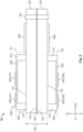
- a sensor assembly 10 according to an embodiment is shown in Figure 1 .
- the sensor assembly 10 includes a substrate 100, a first die 200 attached to the substrate 100, a second die 300 attached to the substrate 100, a full-bridge pressure sensor 400 disposed on the first die 200 and the second die 300, and an integrated circuit 500 connected to the full-bridge pressure sensor 400.
- the substrate 100 has a first outer surface 112 and a second outer surface 116 opposite the first outer surface 112 in a first direction D1, shown in Figure 1 .
- the substrate 100 may be a silicon material, a glass material, a sapphire material, or any other type of material used in piezoresistive sensor substrates.
- the substrate 100 includes a first portion 120 and a second portion 130 formed separately from one another and bonded together at a bond 140.
- the first portion 120 and the second portion 130 are each formed of the material of the substrate 100.
- the first portion 120 has the first outer surface 112 and a first inner surface 122 opposite the first outer surface 112 in the first direction D1.
- the second portion 130 has the second outer surface 116 and a second inner surface 132 opposite the second outer surface 116 in the first direction D1.
- the first inner surface 122 is bonded to the second inner surface 132 by the bond 140, which may be a fusion bond, an epoxy bond, an anodic bond, a eutectic bond, or any other type of bond that can attach the first portion 120 to the second portion 130.
- the bond 140 may be electrically conductive and form an electrical connection.
- the substrate 100 can be formed monolithically in a single piece with the first outer surface 112 and the second outer surface 116.
- the substrate 100 has a first contact 114 on the first outer surface 112 and a second contact 118 on the second outer surface 116.
- the first contact 114 and the second contact 118 may be formed of any conductive material, such as gold or copper, that permits an external electrical connection.
- the first die 200 has a pair of first supports 210 and a first diaphragm 220 extending between the first supports 210.
- the first diaphragm 220 is deflectable with respect to the first supports 210.
- the first die 200 is formed of a silicon material.
- the first die 200 is monolithically formed in a single piece with the first supports 210 and the first diaphragm 220, and the silicon material of the first die 220 is etched to form the first diaphragm 220.
- the first diaphragm 220 is formed separately from the first supports 210 and is attached to the first supports 210.
- the second die 300 has a pair of second supports 310 and a second diaphragm 320 extending between the second supports 310.
- the second diaphragm 320 is deflectable with respect to the second supports 310.
- the second die 300 is formed of a silicon material.
- the second die 300 is monolithically formed in a single piece with the second supports 310 and the second diaphragm 320, and the silicon material of the second die 300 is etched to form the second diaphragm 320.
- the second diaphragm 320 is formed separately from the second supports 310 and is attached to the second supports 310.
- the first die 200 and the second die 300 are identical.
- the full-bridge pressure sensor 400 includes a plurality of piezoresistive elements 402 disposed on the first die 200 and the second die 300.
- the piezoresistive elements 402 include a first subset 410 of at least two of the piezoresistive elements 402 disposed on the first diaphragm 220 and a second subset 420 of at least two of the piezoresistive elements 402 disposed on the second diaphragm 320.
- the piezoresistive elements 402 are an elemental material that is patterned over or embedded into the silicon material of the first die 200 and the second die 300; the piezoresistive elements 402 can be positioned on a surface of or within the diaphragms 220, 320.
- the elemental material is a positive dopant, such as p-type boron, but could be any type of material used to create a piezoresistor in a silicon material.
- the full-bridge pressure sensor 400 includes four piezoresistive elements 402 in the shown embodiment that form a full Wheatstone bridge.
- the first subset 410 is a first half-bridge that includes two piezoresistive elements 402 on the first diaphragm 220 and the second subset 420 is a second half-bridge that includes another two piezoresistive elements 402 on the second diaphragm 320, as shown in Figure 1 .
- the integrated circuit 500 has a processor 510 and a memory 520 connected to the processor 510.
- the memory 520 is a non-transitory computer-readable medium storing algorithms that, when executed by the processor 510, perform the functions of the integrated circuit 500 described herein.
- the integrated circuit 500 can be any kind of application-specific integrated circuit (ASIC) or application-specific standard product (ASSP) chip that is capable of being used in piezoresitive sensor applications as described herein.
- ASIC application-specific integrated circuit
- ASSP application-specific standard product
- the first die 200 is attached to the first outer surface 112 and the second die 300 is attached to the second outer surface 116.
- the first supports 310 of the first die 200 are bonded to the first outer surface 112, for example by fusion bonding, anodic bonding, thermal compression, or solder, and separate the first diaphragm 220 from the first outer surface 112 in the first direction D 1.
- the first diaphragm 220 with the first subset 410 of the piezoresistive elements 402 is deflectable toward the first outer surface 112 in the first direction D1.
- the second supports 310 of the second die 300 are bonded to the second outer surface 116, for example by fusion bonding, anodic bonding, thermal compression, or solder, and separate the second diaphragm 320 from the second outer surface 116 in the first direction D1.
- the second diaphragm 320 with the second subset 420 of piezoresistive elements 402 is deflectable toward the second outer surface 116 in the first direction D1.
- the first subset 410 of piezoresistive elements 402 are disposed on a side of the first diaphragm 220 facing away from the first outer surface 112 in the first direction D1 and the second subset 420 of piezoresistive elements 402 are disposed on a side of the second diaphragm 320 facing away from the second outer surface 116 in the first direction D1.
- the first subset 410 may be disposed on a side of the first diaphragm 220 facing the first outer surface 112 and/or the second subset 420 may be disposed on a side of the second diaphragm 320 facing the second outer surface 116.
- first subset 410 can be embedded within the first diaphragm 220 and/or the second subset 420 can be embedded within the second diaphragm 320.
- first contact 114 can alternatively be positioned on the first diaphragm 220 and the second contact 118 can be positioned on the second diaphragm 320.
- the first subset 410 on the first diaphragm 220 lies in a first plane P1 normal to the first direction D1 and parallel to the first outer surface 112, and the second subset 420 on the second diaphragm 320 lies in a second plane P2 normal to the first direction D1 and parallel to the second outer surface 116.
- the first plane P1 is separated from the second plane P2 in the first direction D1.
- the first die 200 with the first subset 410 and the second die 300 with the second subset 420 are mirror symmetrical about the substrate 100.
- the integrated circuit 500 has a pair of electrical leads 530 connected to the first contact 114 and the second contact 118.
- the integrated circuit 500 is electrically connected to the piezoresistive elements 402 of the first subset 410 and the second subset 420 through the contacts 114, 118.
- the integrated circuit 500 is external to and spaced apart from the substrate 100, the first die 200, and the second die 300.
- the pressure causes deflection of the first diaphragm 220 and the second diaphragm 320, which changes a resistance of the first subset 410 and the second subset 420 of the piezoresistive elements 402 forming the full-bridge pressure sensor 400.
- the first subset 410 or first half-bridge is electrically connected to the first contact 114 and a first signal 540 representing the change in resistance of the first subset 410 that corresponds to the pressure measured by the first subset 410 is transmitted to the integrated circuit 500 through the first contact 114 and one of the electrical leads 530.
- the second subset 420 or second half-bridge is electrically connected to the second contact 118 and a second signal 550 representing the same applied pressure is transmitted to the integrated circuit 500 through the second contact 118 and one of the electrical leads 530.
- the integrated circuit 500 has a calibration algorithm stored on the memory 520 that, when executed by the processor 510, corrects a signal error between the first signal 540 and the second signal 550.
- the processor 510 retrieves a calibrated value stored in the memory 520 based on known temperature and pressure and compares it to the signals 540, 550 to generate the correct compensation for the signal error.
- the integrated circuit 500 combines the first signal 540 and the second signal 550 to output a measured pressure 560 applied to the sensor assembly 10 and measured by the full bridge pressure sensor 400.
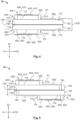
- FIG. 2-6 Other exemplary embodiments of the sensor assembly 10 are shown in Figures 2-6 .
- Like reference numbers refer to like elements with respect to the embodiment of the sensor assembly 10 shown in Figure 1 , and primarily the differences of the embodiments in Figures 2-6 will be described in detail.
- the integrated circuit 500 is positioned or interposed between the first portion 120 and the second portion 130 of the substrate 100.
- the first inner surface 122 of the first portion 120 is attached or bonded to a first side of the integrated circuit 500 and the second inner surface 132 is attached or bonded to a second side of the integrated circuit 500 opposite the first side in the first direction D1.
- the integrated circuit 500 disposed between the portions 120, 130 of the substrate 110 is electrically connected to the first subset 410 and the second subset 420 of the full-bridge pressure sensor 400 by a via 150.
- the via 150 extends from the first outer surface 112 to the second outer surface 116 of the substrate 100, through the first portion 120, the integrated circuit 500, and the second portion 130.
- the via 150 is a passageway through the portions 120, 130 and the integrated circuit 500 that is plated with an electrically conductive material, such as copper.
- the sensor assembly 10 includes a first integrated circuit 502 and a second integrated circuit 504 that each include the components of the integrated circuit 500 described above.
- the first integrated circuit 502 is disposed on the first outer surface 112 adjacent to the first die 200 and the second integrated circuit 504 is disposed on the second outer surface 116 adjacent to the second die 300.
- the first integrated circuit 502 is connected to the first subset 410 and processes the signal from the first subset 410 while the second integrated circuit 504 is connected to the second subset 420 and processes the signal from the second subset 420.
- the integrated circuits 502, 504 are further connected to one another, with either or both of the integrated circuits 502, 504 capable of performing the aforementioned correction of signal error and outputting of the measured pressure 560 sensed by the full-bridge pressure sensor 400.
- the sensor assembly 10 can include one of the first integrated circuit 502 disposed on the first outer surface 112 or the second integrated circuit 504 disposed on the second outer surface 116.
- the dies 200, 300 and the integrated circuits 502, 504 are positioned mirror symmetrical about the substrate 100.
- the dies 200, 300 and the integrated circuits 502, 504 are offset from one another in a second direction D2 perpendicular to the first direction D1 and parallel to the first outer surface 112 and the second outer surface 116.
- the piezoresistive elements 402 of the full-bridge pressure sensor 400 and the integrated circuits 502, 504 are electrically connected by the via 150.
- the via 150 can extend straight through the portions 120, 130 of the substrate 100 in the first direction D1, as shown in Figure 3 , or can have different sections in the portions 120, 130 that are electrically connected and offset from one another in the second direction D2, as shown in Figure 5 .
- the piezoresistive elements 402 of the full-bridge pressure sensor 400 and the integrated circuits 502, 504 are electrically connected by external electrical leads 530 connecting contacts 114, 118 on the outer surfaces 112, 116 of the substrate 100, as similarly described with respect to Figure 1 above.
- At least one of the first supports 210 is sufficiently wide in the second direction D2 that the first integrated circuit 502 and the first contact 114 are disposed on a surface of the first die 200.
- the first integrated circuit 502 and the first contact 114 are aligned with the first support 120 in the first direction D1 and spaced apart from the first diaphragm 220 in the second direction D2.
- at least one of the second supports 310 is sufficiently wide in the second direction D2 that the second integrated circuit 504 and the second contact 118 are disposed on a surface of the second die 300.
- the second integrated circuit 504 and the second contact 118 are aligned with the second support 310 in the first direction D1 and spaced apart from the second diaphragm 320 in the second direction D2.
- splitting the piezoresistors 402 of the full-bridge pressure sensor 400 into the first subset 410 and the second subset 420 positioned on different diaphragms 220, 320 and attaching the dies 200, 300 having the diaphragms 220, 320 to the substrate 100 in a stacked orientation in the first direction D1 decreases the overall size or footprint of the sensor assembly 10.
- Combining the signals 540, 550 from the two subsets 410, 420 into the measured pressure 560 allows for the increased sensitivity and performance of a full-bridge pressure sensor 400 while significantly decreasing the necessary overall size of the sensor assembly 10, permitting greater accuracy of pressure measurements in size-restricted applications.
Landscapes
- Physics & Mathematics (AREA)
- General Physics & Mathematics (AREA)
- Chemical & Material Sciences (AREA)
- Analytical Chemistry (AREA)
- Health & Medical Sciences (AREA)
- Engineering & Computer Science (AREA)
- Biomedical Technology (AREA)
- Measuring Fluid Pressure (AREA)
- Pressure Sensors (AREA)
Abstract
Description
- The present invention relates to a sensor and, more particularly, to a sensor assembly including a full-bridge pressure sensor.
- A pressure sensor commonly includes a sensor diaphragm and piezoresistors disposed on the sensor diaphragm. An applied force or pressure deflects the sensor diaphragm, which changes the resistance of the piezoresistors on the diaphragm, correspondingly changing a measured output of the pressure sensor that reflects the force or pressure.
- A full-bridge pressure sensor is used to increase the accuracy and reliability of the sensor measurements. The full-bridge sensor, however, requires a sensor diaphragm sized to accommodate four piezoresistors to form the full Wheatstone bridge, which increases the necessary size of the pressure sensor. Current solutions cannot provide the accuracy and performance of a full-bridge sensor in applications, such as medical applications, that have significant size restrictions.
- A sensor assembly includes a substrate having a first outer surface and a second outer surface opposite the first outer surface, a first die attached to the first outer surface and having a first diaphragm, a second die attached to the second outer surface and having a second diaphragm, and a full-bridge pressure sensor including a plurality of piezoresistive elements. A first subset of at least two of the plurality of piezoresistive elements is disposed on the first diaphragm and a second subset of at least two of the plurality of piezoresistive elements is disposed on the second diaphragm.
- The invention will now be described by way of example with reference to the accompanying Figures, of which:
-
Figure 1 is a schematic diagram of a sensor assembly according to an embodiment; -
Figure 2 is a schematic diagram of a sensor assembly according to another embodiment; -
Figure 3 is a schematic diagram of a sensor assembly according to another embodiment; -
Figure 4 is a schematic diagram of a sensor assembly according to another embodiment; -
Figure 5 is a schematic diagram of a sensor assembly according to another embodiment; and -
Figure 6 is a schematic diagram of a sensor assembly according to another embodiment. - Exemplary embodiments of the present disclosure will be described hereinafter in detail with reference to the attached drawings, wherein like reference numerals refer to like elements. The present disclosure may, however, be embodied in many different forms and should not be construed as being limited to the embodiments set forth herein; rather, these embodiments are provided so that the present disclosure will convey the concept of the disclosure to those skilled in the art. In addition, in the following detailed description, for purposes of explanation, numerous specific details are set forth to provide a thorough understanding of the disclosed embodiments. However, it is apparent that one or more embodiments may also be implemented without these specific details.
- Throughout the drawings, only one of a plurality of identical elements may be labeled in a figure for clarity of the drawings, but the detailed description of the element herein applies equally to each of the identically appearing elements in the figure. Directional descriptors used in the specification are merely for clarity of the description and for differentiation of the various directions. These directional descriptors do not imply or require any particular orientation of the disclosed elements.
- A
sensor assembly 10 according to an embodiment is shown inFigure 1 . Thesensor assembly 10 includes asubstrate 100, afirst die 200 attached to thesubstrate 100, asecond die 300 attached to thesubstrate 100, a full-bridge pressure sensor 400 disposed on thefirst die 200 and thesecond die 300, and anintegrated circuit 500 connected to the full-bridge pressure sensor 400. - The
substrate 100 has a firstouter surface 112 and a secondouter surface 116 opposite the firstouter surface 112 in a first direction D1, shown inFigure 1 . Thesubstrate 100 may be a silicon material, a glass material, a sapphire material, or any other type of material used in piezoresistive sensor substrates. - In the embodiment shown in
Figure 1 , thesubstrate 100 includes afirst portion 120 and asecond portion 130 formed separately from one another and bonded together at abond 140. Thefirst portion 120 and thesecond portion 130 are each formed of the material of thesubstrate 100. Thefirst portion 120 has the firstouter surface 112 and a firstinner surface 122 opposite the firstouter surface 112 in the first direction D1. Thesecond portion 130 has the secondouter surface 116 and a secondinner surface 132 opposite the secondouter surface 116 in the first direction D1. The firstinner surface 122 is bonded to the secondinner surface 132 by thebond 140, which may be a fusion bond, an epoxy bond, an anodic bond, a eutectic bond, or any other type of bond that can attach thefirst portion 120 to thesecond portion 130. In some embodiments, thebond 140 may be electrically conductive and form an electrical connection. In another embodiment, thesubstrate 100 can be formed monolithically in a single piece with the firstouter surface 112 and the secondouter surface 116. - As shown in the embodiment of
Figure 1 , thesubstrate 100 has afirst contact 114 on the firstouter surface 112 and asecond contact 118 on the secondouter surface 116. Thefirst contact 114 and thesecond contact 118 may be formed of any conductive material, such as gold or copper, that permits an external electrical connection. - The
first die 200, as shown inFigure 1 , has a pair offirst supports 210 and afirst diaphragm 220 extending between thefirst supports 210. Thefirst diaphragm 220 is deflectable with respect to thefirst supports 210. The first die 200 is formed of a silicon material. In an embodiment, thefirst die 200 is monolithically formed in a single piece with thefirst supports 210 and thefirst diaphragm 220, and the silicon material of thefirst die 220 is etched to form thefirst diaphragm 220. In another embodiment, thefirst diaphragm 220 is formed separately from thefirst supports 210 and is attached to thefirst supports 210. - The
second die 300, as shown inFigure 1 , has a pair ofsecond supports 310 and asecond diaphragm 320 extending between thesecond supports 310. Thesecond diaphragm 320 is deflectable with respect to thesecond supports 310. The second die 300 is formed of a silicon material. In an embodiment, thesecond die 300 is monolithically formed in a single piece with thesecond supports 310 and thesecond diaphragm 320, and the silicon material of thesecond die 300 is etched to form thesecond diaphragm 320. In another embodiment, thesecond diaphragm 320 is formed separately from thesecond supports 310 and is attached to thesecond supports 310. In an embodiment, the first die 200 and the second die 300 are identical. - The full-
bridge pressure sensor 400, as shown inFigure 1 , includes a plurality of piezoresistive elements 402 disposed on thefirst die 200 and thesecond die 300. The piezoresistive elements 402 include a first subset 410 of at least two of the piezoresistive elements 402 disposed on thefirst diaphragm 220 and a second subset 420 of at least two of the piezoresistive elements 402 disposed on thesecond diaphragm 320. The piezoresistive elements 402 are an elemental material that is patterned over or embedded into the silicon material of thefirst die 200 and thesecond die 300; the piezoresistive elements 402 can be positioned on a surface of or within thediaphragms - The full-
bridge pressure sensor 400 includes four piezoresistive elements 402 in the shown embodiment that form a full Wheatstone bridge. In this embodiment, the first subset 410 is a first half-bridge that includes two piezoresistive elements 402 on thefirst diaphragm 220 and the second subset 420 is a second half-bridge that includes another two piezoresistive elements 402 on thesecond diaphragm 320, as shown inFigure 1 . - As shown in
Figure 1 , theintegrated circuit 500 has aprocessor 510 and amemory 520 connected to theprocessor 510. Thememory 520 is a non-transitory computer-readable medium storing algorithms that, when executed by theprocessor 510, perform the functions of theintegrated circuit 500 described herein. The integratedcircuit 500 can be any kind of application-specific integrated circuit (ASIC) or application-specific standard product (ASSP) chip that is capable of being used in piezoresitive sensor applications as described herein. - In the
sensor assembly 10 shown inFigure 1 , thefirst die 200 is attached to the firstouter surface 112 and thesecond die 300 is attached to the secondouter surface 116. Thefirst supports 310 of thefirst die 200 are bonded to the firstouter surface 112, for example by fusion bonding, anodic bonding, thermal compression, or solder, and separate thefirst diaphragm 220 from the firstouter surface 112 in the first direction D 1. Thefirst diaphragm 220 with the first subset 410 of the piezoresistive elements 402 is deflectable toward the firstouter surface 112 in the first direction D1. Thesecond supports 310 of thesecond die 300 are bonded to the secondouter surface 116, for example by fusion bonding, anodic bonding, thermal compression, or solder, and separate thesecond diaphragm 320 from the secondouter surface 116 in the first direction D1. Thesecond diaphragm 320 with the second subset 420 of piezoresistive elements 402 is deflectable toward the secondouter surface 116 in the first direction D1. - In the shown embodiment, the first subset 410 of piezoresistive elements 402 are disposed on a side of the
first diaphragm 220 facing away from the firstouter surface 112 in the first direction D1 and the second subset 420 of piezoresistive elements 402 are disposed on a side of thesecond diaphragm 320 facing away from the secondouter surface 116 in the first direction D1. In another embodiment, the first subset 410 may be disposed on a side of thefirst diaphragm 220 facing the firstouter surface 112 and/or the second subset 420 may be disposed on a side of thesecond diaphragm 320 facing the secondouter surface 116. In another embodiment, the first subset 410 can be embedded within thefirst diaphragm 220 and/or the second subset 420 can be embedded within thesecond diaphragm 320. In another embodiment, thefirst contact 114 can alternatively be positioned on thefirst diaphragm 220 and thesecond contact 118 can be positioned on thesecond diaphragm 320. - The first subset 410 on the
first diaphragm 220 lies in a first plane P1 normal to the first direction D1 and parallel to the firstouter surface 112, and the second subset 420 on thesecond diaphragm 320 lies in a second plane P2 normal to the first direction D1 and parallel to the secondouter surface 116. As shown inFigure 1 , the first plane P1 is separated from the second plane P2 in the first direction D1. In the embodiment of thesensor assembly 10 shown inFigure 1 , thefirst die 200 with the first subset 410 and thesecond die 300 with the second subset 420 are mirror symmetrical about thesubstrate 100. - The
integrated circuit 500, as shown inFigure 1 , has a pair ofelectrical leads 530 connected to thefirst contact 114 and thesecond contact 118. Theintegrated circuit 500 is electrically connected to the piezoresistive elements 402 of the first subset 410 and the second subset 420 through thecontacts Figure 1 , theintegrated circuit 500 is external to and spaced apart from thesubstrate 100, thefirst die 200, and thesecond die 300. - In use of the
sensor assembly 10 to measure a force or pressure, the pressure causes deflection of thefirst diaphragm 220 and thesecond diaphragm 320, which changes a resistance of the first subset 410 and the second subset 420 of the piezoresistive elements 402 forming the full-bridge pressure sensor 400. The first subset 410 or first half-bridge is electrically connected to thefirst contact 114 and afirst signal 540 representing the change in resistance of the first subset 410 that corresponds to the pressure measured by the first subset 410 is transmitted to theintegrated circuit 500 through thefirst contact 114 and one of the electrical leads 530. The second subset 420 or second half-bridge is electrically connected to thesecond contact 118 and asecond signal 550 representing the same applied pressure is transmitted to theintegrated circuit 500 through thesecond contact 118 and one of the electrical leads 530. - Even though the first subset 410 and the second subset 420 act as a full-
bridge sensor 400 to measure the same pressure applied to thesensor assembly 10, because the first subset 410 and the second subset 420 are positioned in the planes P1, P2 spaced apart from one another, thefirst signal 540 and thesecond signal 550 may have some difference due to positional variations in the applied pressure. Theintegrated circuit 500 has a calibration algorithm stored on thememory 520 that, when executed by theprocessor 510, corrects a signal error between thefirst signal 540 and thesecond signal 550. Theprocessor 510 retrieves a calibrated value stored in thememory 520 based on known temperature and pressure and compares it to thesignals integrated circuit 500 combines thefirst signal 540 and thesecond signal 550 to output a measuredpressure 560 applied to thesensor assembly 10 and measured by the fullbridge pressure sensor 400. - Other exemplary embodiments of the
sensor assembly 10 are shown inFigures 2-6 . Like reference numbers refer to like elements with respect to the embodiment of thesensor assembly 10 shown inFigure 1 , and primarily the differences of the embodiments inFigures 2-6 will be described in detail. - In the
sensor assembly 10 shown inFigure 2 , theintegrated circuit 500 is positioned or interposed between thefirst portion 120 and thesecond portion 130 of thesubstrate 100. The firstinner surface 122 of thefirst portion 120 is attached or bonded to a first side of theintegrated circuit 500 and the secondinner surface 132 is attached or bonded to a second side of theintegrated circuit 500 opposite the first side in the first direction D1. - In the embodiment shown in
Figure 2 , instead of thecontacts Figure 1 , theintegrated circuit 500 disposed between theportions bridge pressure sensor 400 by a via 150. The via 150 extends from the firstouter surface 112 to the secondouter surface 116 of thesubstrate 100, through thefirst portion 120, theintegrated circuit 500, and thesecond portion 130. In an embodiment, the via 150 is a passageway through theportions integrated circuit 500 that is plated with an electrically conductive material, such as copper. - In the embodiments shown in
Figures 3-6 , thesensor assembly 10 includes a firstintegrated circuit 502 and a secondintegrated circuit 504 that each include the components of theintegrated circuit 500 described above. The firstintegrated circuit 502 is disposed on the firstouter surface 112 adjacent to thefirst die 200 and the secondintegrated circuit 504 is disposed on the secondouter surface 116 adjacent to thesecond die 300. The firstintegrated circuit 502 is connected to the first subset 410 and processes the signal from the first subset 410 while the secondintegrated circuit 504 is connected to the second subset 420 and processes the signal from the second subset 420. Theintegrated circuits integrated circuits pressure 560 sensed by the full-bridge pressure sensor 400. In another embodiment, thesensor assembly 10 can include one of the firstintegrated circuit 502 disposed on the firstouter surface 112 or the secondintegrated circuit 504 disposed on the secondouter surface 116. - In the embodiments shown in
Figures 3 and4 , the dies 200, 300 and theintegrated circuits substrate 100. In another embodiment shown inFigure 5 , the dies 200, 300 and theintegrated circuits outer surface 112 and the secondouter surface 116. - In the embodiments of
Figures 3 and5 , the piezoresistive elements 402 of the full-bridge pressure sensor 400 and theintegrated circuits via 150. The via 150 can extend straight through theportions substrate 100 in the first direction D1, as shown inFigure 3 , or can have different sections in theportions Figure 5 . In the embodiment ofFigure 4 , the piezoresistive elements 402 of the full-bridge pressure sensor 400 and theintegrated circuits electrical leads 530 connectingcontacts outer surfaces substrate 100, as similarly described with respect toFigure 1 above. - In the embodiment of
Figure 6 , at least one of thefirst supports 210 is sufficiently wide in the second direction D2 that the firstintegrated circuit 502 and thefirst contact 114 are disposed on a surface of thefirst die 200. The firstintegrated circuit 502 and thefirst contact 114 are aligned with thefirst support 120 in the first direction D1 and spaced apart from thefirst diaphragm 220 in the second direction D2. Likewise, at least one of thesecond supports 310 is sufficiently wide in the second direction D2 that the secondintegrated circuit 504 and thesecond contact 118 are disposed on a surface of thesecond die 300. The secondintegrated circuit 504 and thesecond contact 118 are aligned with thesecond support 310 in the first direction D1 and spaced apart from thesecond diaphragm 320 in the second direction D2. - In the embodiments of the
sensor assembly 10 described above, splitting the piezoresistors 402 of the full-bridge pressure sensor 400 into the first subset 410 and the second subset 420 positioned ondifferent diaphragms diaphragms substrate 100 in a stacked orientation in the first direction D1 decreases the overall size or footprint of thesensor assembly 10. Combining thesignals pressure 560 allows for the increased sensitivity and performance of a full-bridge pressure sensor 400 while significantly decreasing the necessary overall size of thesensor assembly 10, permitting greater accuracy of pressure measurements in size-restricted applications.
Claims (15)
- A sensor assembly (10), comprising:a substrate (100) having a first outer surface (112) and a second outer surface (116) opposite the first outer surface (112);a first die (200) attached to the first outer surface (112) and having a first diaphragm (220);a second die (300) attached to the second outer surface (116) and having a second diaphragm (320); anda full-bridge pressure sensor (400) including a plurality of piezoresistive elements (402), a first subset (410) of at least two of the plurality of piezoresistive elements (402) is disposed on or in the first diaphragm (220) and a second subset (420) of at least two of the plurality of piezoresistive elements (402) is disposed on or in the second diaphragm (320).
- The sensor assembly (10) of claim 1, wherein the substrate (100) includes a first portion (120) and a second portion (130), the first portion (120) has the first outer surface (112) and a first inner surface (122) opposite the first outer surface (112), the second portion (130) has the second outer surface (116) and a second inner surface (132) opposite the second outer surface (116), the first inner surface (122) is bonded to the second inner surface (132).
- The sensor assembly (10) of claim 1 or 2, wherein the first die (200) has a pair of first supports (210) attached to the first outer surface (112) and separating the first diaphragm (220) from the first outer surface (112), the first diaphragm (220) is deflectable toward the first outer surface (112), the second die (300) has a pair of second supports (310) attached to the second outer surface (116) and separating the second diaphragm (320) from the second outer surface (116), the second diaphragm (320) is deflectable toward the second outer surface (116).
- The sensor assembly (10) of any preceding claim, wherein the second die (300) is mirror symmetrical to the first die (200) about the substrate (100), or the second die (300) is offset from the first die (200) in a direction parallel to the first outer surface (112) and the second outer surface (116).
- The sensor assembly (10) of any preceding claim, further comprising an integrated circuit (500), the first subset (410) and the second subset (420) of the piezoresistive elements (402) are connected to the integrated circuit (500), the integrated circuit (500) receives a first signal (540) from the first subset (410) and a second signal (550) from the second subset (420), the integrated circuit (500) corrects a signal error between the first signal (540) and the second signal (550) measuring a pressure around the sensor assembly (10).
- The sensor assembly (10) of claim 5, wherein the substrate (100) includes a first portion (120) and a second portion (130), the first portion (120) has the first outer surface (112) and a first inner surface (122) opposite the first outer surface (112), the second portion (130) has the second outer surface (116) and a second inner surface (132) opposite the second outer surface (116), the integrated circuit (500) is interposed between the first inner surface (122) and the second inner surface (132).
- The sensor assembly (10) of claim 5, wherein the integrated circuit (500) is disposed on at least one of the first outer surface (112) and the second outer surface (116).
- The sensor assembly (10) of claim 7, wherein the integrated circuit (500) is a first integrated circuit (502) disposed on the first outer surface (112) and further comprising a second integrated circuit (504) disposed on the second outer surface (116).
- The sensor assembly (10) of claim 5 or any claim depending thereon, wherein the substrate (100) has a via (150) extending through the substrate (100) from the first outer surface (112) to the second outer surface (116), the via (150) electrically connects the first subset (410) and the second subset (420) with the integrated circuit (500).
- The sensor assembly (10) of claim 5, wherein the integrated circuit (500) is external to and spaced apart from the substrate (100), the first die (200), and the second die (300).
- The sensor assembly (10) of claim 5 or any claim depending thereon, wherein the first outer surface (112) has a first contact (114) and the second outer surface (116) has a second contact (118), the integrated circuit (500) is electrically connected to the first subset (410) and the second subset (420) through the first contact (114) and the second contact (118).
- The sensor assembly (10) of any preceding claim, wherein the first subset (410) is disposed on a side of the first diaphragm (220) facing the first outer surface (112) and/or the second subset (420) is disposed on a side of the second diaphragm (320) facing the second outer surface (116).
- The sensor assembly (10) of any preceding claim, wherein first die (200) and the second die (300) are each a silicon material, the piezoresistive elements (402) are an elemental material patterned over or embedded into the silicon material of the first die (200) and the second die (300).
- The sensor assembly (10) of any preceding claim, wherein the full-bridge pressure sensor (400) includes four piezoresistive elements (402), the first subset (410) is a first half-bridge of two piezoresistive elements on or in the first diaphragm (220) and the second subset (420) is a second half-bridge of two piezoresistive elements on or in the second diaphragm (320).
- The sensor assembly (10) of any preceding claim, wherein the first subset (410) on or in the first diaphragm (220) lies in a first plane (P1) parallel to the first outer surface (112) and the second subset (420) on or in the second diaphragm (320) lies in a second plane (P2) parallel to the second outer surface (116), the first plane (P1) is separated from the second plane (P2).
Applications Claiming Priority (1)
| Application Number | Priority Date | Filing Date | Title |
|---|---|---|---|
| US18/155,836 US20240241004A1 (en) | 2023-01-18 | 2023-01-18 | Sensor assembly with a full-bridge pressure sensor |
Publications (2)
| Publication Number | Publication Date |
|---|---|
| EP4403895A1 true EP4403895A1 (en) | 2024-07-24 |
| EP4403895B1 EP4403895B1 (en) | 2025-06-04 |
Family
ID=89620697
Family Applications (1)
| Application Number | Title | Priority Date | Filing Date |
|---|---|---|---|
| EP24152333.1A Active EP4403895B1 (en) | 2023-01-18 | 2024-01-17 | Split-stacked full-bridge pressure sensor |
Country Status (3)
| Country | Link |
|---|---|
| US (1) | US20240241004A1 (en) |
| EP (1) | EP4403895B1 (en) |
| CN (1) | CN118362226A (en) |
Cited By (1)
| Publication number | Priority date | Publication date | Assignee | Title |
|---|---|---|---|---|
| DE102024202674A1 (en) * | 2024-03-21 | 2025-09-25 | Robert Bosch Gesellschaft mit beschränkter Haftung | Micromechanical pressure sensor |
Citations (4)
| Publication number | Priority date | Publication date | Assignee | Title |
|---|---|---|---|---|
| EP2112488A2 (en) * | 2008-04-24 | 2009-10-28 | Fujikura, Ltd. | Pressure sensor module and electronic component |
| US8171800B1 (en) * | 2011-01-25 | 2012-05-08 | Continental Automotive Systems, Inc. | Differential pressure sensor using dual backside absolute pressure sensing |
| EP3196618A2 (en) * | 2016-01-20 | 2017-07-26 | Rosemount Aerospace Inc. | Pseudo differential pressure sensing bridge configuration |
| EP3982097A1 (en) * | 2020-10-07 | 2022-04-13 | Honeywell International Inc. | Differential pressure sensor and method of using the same |
-
2023
- 2023-01-18 US US18/155,836 patent/US20240241004A1/en not_active Abandoned
-
2024
- 2024-01-17 EP EP24152333.1A patent/EP4403895B1/en active Active
- 2024-01-17 CN CN202410074169.5A patent/CN118362226A/en active Pending
Patent Citations (4)
| Publication number | Priority date | Publication date | Assignee | Title |
|---|---|---|---|---|
| EP2112488A2 (en) * | 2008-04-24 | 2009-10-28 | Fujikura, Ltd. | Pressure sensor module and electronic component |
| US8171800B1 (en) * | 2011-01-25 | 2012-05-08 | Continental Automotive Systems, Inc. | Differential pressure sensor using dual backside absolute pressure sensing |
| EP3196618A2 (en) * | 2016-01-20 | 2017-07-26 | Rosemount Aerospace Inc. | Pseudo differential pressure sensing bridge configuration |
| EP3982097A1 (en) * | 2020-10-07 | 2022-04-13 | Honeywell International Inc. | Differential pressure sensor and method of using the same |
Cited By (1)
| Publication number | Priority date | Publication date | Assignee | Title |
|---|---|---|---|---|
| DE102024202674A1 (en) * | 2024-03-21 | 2025-09-25 | Robert Bosch Gesellschaft mit beschränkter Haftung | Micromechanical pressure sensor |
Also Published As
| Publication number | Publication date |
|---|---|
| US20240241004A1 (en) | 2024-07-18 |
| EP4403895B1 (en) | 2025-06-04 |
| CN118362226A (en) | 2024-07-19 |
Similar Documents
| Publication | Publication Date | Title |
|---|---|---|
| KR101953454B1 (en) | Pressure sensor chip | |
| KR101953455B1 (en) | Pressure sensor | |
| US8806964B2 (en) | Force sensor | |
| US6062088A (en) | Pressure sensor | |
| US4574640A (en) | Integrated dual-range pressure transducer | |
| US20100083764A1 (en) | Redundant self compensating leadless pressure sensor | |
| JPH0425735A (en) | Semiconductor pressure/differential pressure measurement diaphragm | |
| CN104006914A (en) | Systems and methods for a pressure sensor having a two layer die structure | |
| EP4403895B1 (en) | Split-stacked full-bridge pressure sensor | |
| US20240302236A1 (en) | Sensor Package With A Sensor Die | |
| JP2895262B2 (en) | Composite sensor | |
| CN118089999B (en) | Pressure sensor, pressure sensing device and electronic device | |
| JP2009265012A (en) | Semiconductor sensor | |
| KR101573367B1 (en) | Piezoresistive typed ceramic pressure sensor | |
| CN219369005U (en) | Capacitive pressure sensor | |
| US11344207B2 (en) | Pressure pulse wave sensor and biological information measurement device | |
| US12436049B2 (en) | Sensor die with a diaphragm | |
| KR102382142B1 (en) | Pressure Sensor Package Using One Mold Package | |
| JP2005010021A (en) | Differential pressure transmitter | |
| JPH02196938A (en) | Pressure sensor | |
| JP2512220B2 (en) | Multi-function sensor | |
| JPH10132682A (en) | Semiconductor pressure sensor, method of manufacturing the same, and composite transmitter using the same | |
| JP3120388B2 (en) | Semiconductor pressure transducer | |
| EP1552260B1 (en) | Pressure sensor and production thereof | |
| JP2008116287A (en) | Pressure sensor |
Legal Events
| Date | Code | Title | Description |
|---|---|---|---|
| PUAI | Public reference made under article 153(3) epc to a published international application that has entered the european phase |
Free format text: ORIGINAL CODE: 0009012 |
|
| STAA | Information on the status of an ep patent application or granted ep patent |
Free format text: STATUS: THE APPLICATION HAS BEEN PUBLISHED |
|
| AK | Designated contracting states |
Kind code of ref document: A1 Designated state(s): AL AT BE BG CH CY CZ DE DK EE ES FI FR GB GR HR HU IE IS IT LI LT LU LV MC ME MK MT NL NO PL PT RO RS SE SI SK SM TR |
|
| STAA | Information on the status of an ep patent application or granted ep patent |
Free format text: STATUS: REQUEST FOR EXAMINATION WAS MADE |
|
| 17P | Request for examination filed |
Effective date: 20250121 |
|
| GRAP | Despatch of communication of intention to grant a patent |
Free format text: ORIGINAL CODE: EPIDOSNIGR1 |
|
| STAA | Information on the status of an ep patent application or granted ep patent |
Free format text: STATUS: GRANT OF PATENT IS INTENDED |
|
| INTG | Intention to grant announced |
Effective date: 20250305 |
|
| GRAS | Grant fee paid |
Free format text: ORIGINAL CODE: EPIDOSNIGR3 |
|
| GRAA | (expected) grant |
Free format text: ORIGINAL CODE: 0009210 |
|
| STAA | Information on the status of an ep patent application or granted ep patent |
Free format text: STATUS: THE PATENT HAS BEEN GRANTED |
|
| AK | Designated contracting states |
Kind code of ref document: B1 Designated state(s): AL AT BE BG CH CY CZ DE DK EE ES FI FR GB GR HR HU IE IS IT LI LT LU LV MC ME MK MT NL NO PL PT RO RS SE SI SK SM TR |
|
| REG | Reference to a national code |
Ref country code: GB Ref legal event code: FG4D |
|
| REG | Reference to a national code |
Ref country code: CH Ref legal event code: EP |
|
| REG | Reference to a national code |
Ref country code: DE Ref legal event code: R096 Ref document number: 602024000164 Country of ref document: DE |
|
| REG | Reference to a national code |
Ref country code: IE Ref legal event code: FG4D |
|
| REG | Reference to a national code |
Ref country code: NL Ref legal event code: MP Effective date: 20250604 |
|
| PG25 | Lapsed in a contracting state [announced via postgrant information from national office to epo] |
Ref country code: FI Free format text: LAPSE BECAUSE OF FAILURE TO SUBMIT A TRANSLATION OF THE DESCRIPTION OR TO PAY THE FEE WITHIN THE PRESCRIBED TIME-LIMIT Effective date: 20250604 Ref country code: ES Free format text: LAPSE BECAUSE OF FAILURE TO SUBMIT A TRANSLATION OF THE DESCRIPTION OR TO PAY THE FEE WITHIN THE PRESCRIBED TIME-LIMIT Effective date: 20250604 |
|
| REG | Reference to a national code |
Ref country code: LT Ref legal event code: MG9D |
|
| PG25 | Lapsed in a contracting state [announced via postgrant information from national office to epo] |
Ref country code: NO Free format text: LAPSE BECAUSE OF FAILURE TO SUBMIT A TRANSLATION OF THE DESCRIPTION OR TO PAY THE FEE WITHIN THE PRESCRIBED TIME-LIMIT Effective date: 20250904 Ref country code: GR Free format text: LAPSE BECAUSE OF FAILURE TO SUBMIT A TRANSLATION OF THE DESCRIPTION OR TO PAY THE FEE WITHIN THE PRESCRIBED TIME-LIMIT Effective date: 20250905 |
|
| PG25 | Lapsed in a contracting state [announced via postgrant information from national office to epo] |
Ref country code: PL Free format text: LAPSE BECAUSE OF FAILURE TO SUBMIT A TRANSLATION OF THE DESCRIPTION OR TO PAY THE FEE WITHIN THE PRESCRIBED TIME-LIMIT Effective date: 20250604 |
|
| PG25 | Lapsed in a contracting state [announced via postgrant information from national office to epo] |
Ref country code: BG Free format text: LAPSE BECAUSE OF FAILURE TO SUBMIT A TRANSLATION OF THE DESCRIPTION OR TO PAY THE FEE WITHIN THE PRESCRIBED TIME-LIMIT Effective date: 20250604 |
|
| PG25 | Lapsed in a contracting state [announced via postgrant information from national office to epo] |
Ref country code: HR Free format text: LAPSE BECAUSE OF FAILURE TO SUBMIT A TRANSLATION OF THE DESCRIPTION OR TO PAY THE FEE WITHIN THE PRESCRIBED TIME-LIMIT Effective date: 20250604 |
|
| PG25 | Lapsed in a contracting state [announced via postgrant information from national office to epo] |
Ref country code: RS Free format text: LAPSE BECAUSE OF FAILURE TO SUBMIT A TRANSLATION OF THE DESCRIPTION OR TO PAY THE FEE WITHIN THE PRESCRIBED TIME-LIMIT Effective date: 20250904 |
|
| PG25 | Lapsed in a contracting state [announced via postgrant information from national office to epo] |
Ref country code: LV Free format text: LAPSE BECAUSE OF FAILURE TO SUBMIT A TRANSLATION OF THE DESCRIPTION OR TO PAY THE FEE WITHIN THE PRESCRIBED TIME-LIMIT Effective date: 20250604 |
|
| PG25 | Lapsed in a contracting state [announced via postgrant information from national office to epo] |
Ref country code: NL Free format text: LAPSE BECAUSE OF FAILURE TO SUBMIT A TRANSLATION OF THE DESCRIPTION OR TO PAY THE FEE WITHIN THE PRESCRIBED TIME-LIMIT Effective date: 20250604 |
|
| PG25 | Lapsed in a contracting state [announced via postgrant information from national office to epo] |
Ref country code: PT Free format text: LAPSE BECAUSE OF FAILURE TO SUBMIT A TRANSLATION OF THE DESCRIPTION OR TO PAY THE FEE WITHIN THE PRESCRIBED TIME-LIMIT Effective date: 20251006 |
|
| REG | Reference to a national code |
Ref country code: AT Ref legal event code: MK05 Ref document number: 1800745 Country of ref document: AT Kind code of ref document: T Effective date: 20250604 |
|
| PG25 | Lapsed in a contracting state [announced via postgrant information from national office to epo] |
Ref country code: IS Free format text: LAPSE BECAUSE OF FAILURE TO SUBMIT A TRANSLATION OF THE DESCRIPTION OR TO PAY THE FEE WITHIN THE PRESCRIBED TIME-LIMIT Effective date: 20251004 |
|
| PG25 | Lapsed in a contracting state [announced via postgrant information from national office to epo] |
Ref country code: AT Free format text: LAPSE BECAUSE OF FAILURE TO SUBMIT A TRANSLATION OF THE DESCRIPTION OR TO PAY THE FEE WITHIN THE PRESCRIBED TIME-LIMIT Effective date: 20250604 Ref country code: SM Free format text: LAPSE BECAUSE OF FAILURE TO SUBMIT A TRANSLATION OF THE DESCRIPTION OR TO PAY THE FEE WITHIN THE PRESCRIBED TIME-LIMIT Effective date: 20250604 |
|
| PG25 | Lapsed in a contracting state [announced via postgrant information from national office to epo] |
Ref country code: CZ Free format text: LAPSE BECAUSE OF FAILURE TO SUBMIT A TRANSLATION OF THE DESCRIPTION OR TO PAY THE FEE WITHIN THE PRESCRIBED TIME-LIMIT Effective date: 20250604 |
|
| PG25 | Lapsed in a contracting state [announced via postgrant information from national office to epo] |
Ref country code: EE Free format text: LAPSE BECAUSE OF FAILURE TO SUBMIT A TRANSLATION OF THE DESCRIPTION OR TO PAY THE FEE WITHIN THE PRESCRIBED TIME-LIMIT Effective date: 20250604 |
|
| PG25 | Lapsed in a contracting state [announced via postgrant information from national office to epo] |
Ref country code: SK Free format text: LAPSE BECAUSE OF FAILURE TO SUBMIT A TRANSLATION OF THE DESCRIPTION OR TO PAY THE FEE WITHIN THE PRESCRIBED TIME-LIMIT Effective date: 20250604 |
|
| PG25 | Lapsed in a contracting state [announced via postgrant information from national office to epo] |
Ref country code: IT Free format text: LAPSE BECAUSE OF FAILURE TO SUBMIT A TRANSLATION OF THE DESCRIPTION OR TO PAY THE FEE WITHIN THE PRESCRIBED TIME-LIMIT Effective date: 20250604 |
|
| REG | Reference to a national code |
Ref country code: DE Ref legal event code: R097 Ref document number: 602024000164 Country of ref document: DE |
|
| PLBE | No opposition filed within time limit |
Free format text: ORIGINAL CODE: 0009261 |
|
| STAA | Information on the status of an ep patent application or granted ep patent |
Free format text: STATUS: NO OPPOSITION FILED WITHIN TIME LIMIT |
|
| PG25 | Lapsed in a contracting state [announced via postgrant information from national office to epo] |
Ref country code: DK Free format text: LAPSE BECAUSE OF FAILURE TO SUBMIT A TRANSLATION OF THE DESCRIPTION OR TO PAY THE FEE WITHIN THE PRESCRIBED TIME-LIMIT Effective date: 20250604 |
|
| PGFP | Annual fee paid to national office [announced via postgrant information from national office to epo] |
Ref country code: DE Payment date: 20251203 Year of fee payment: 3 |
|
| REG | Reference to a national code |
Ref country code: CH Ref legal event code: L10 Free format text: ST27 STATUS EVENT CODE: U-0-0-L10-L00 (AS PROVIDED BY THE NATIONAL OFFICE) Effective date: 20260416 |
|
| 26N | No opposition filed |
Effective date: 20260305 |
|
| PG25 | Lapsed in a contracting state [announced via postgrant information from national office to epo] |
Ref country code: LT Free format text: LAPSE BECAUSE OF FAILURE TO SUBMIT A TRANSLATION OF THE DESCRIPTION OR TO PAY THE FEE WITHIN THE PRESCRIBED TIME-LIMIT Effective date: 20250604 |
|
| PG25 | Lapsed in a contracting state [announced via postgrant information from national office to epo] |
Ref country code: SE Free format text: LAPSE BECAUSE OF FAILURE TO SUBMIT A TRANSLATION OF THE DESCRIPTION OR TO PAY THE FEE WITHIN THE PRESCRIBED TIME-LIMIT Effective date: 20250604 |