EP4403536A1 - Multi-component device and method of making a multi-component device - Google Patents
Multi-component device and method of making a multi-component device Download PDFInfo
- Publication number
- EP4403536A1 EP4403536A1 EP23218687.4A EP23218687A EP4403536A1 EP 4403536 A1 EP4403536 A1 EP 4403536A1 EP 23218687 A EP23218687 A EP 23218687A EP 4403536 A1 EP4403536 A1 EP 4403536A1
- Authority
- EP
- European Patent Office
- Prior art keywords
- sic
- polishable
- carbide
- silicon
- substrate
- Prior art date
- Legal status (The legal status is an assumption and is not a legal conclusion. Google has not performed a legal analysis and makes no representation as to the accuracy of the status listed.)
- Pending
Links
- 238000004519 manufacturing process Methods 0.000 title claims abstract description 8
- 239000000758 substrate Substances 0.000 claims abstract description 67
- 239000000463 material Substances 0.000 claims abstract description 42
- 238000000034 method Methods 0.000 claims abstract description 39
- 239000000919 ceramic Substances 0.000 claims abstract description 26
- 229910052710 silicon Inorganic materials 0.000 claims abstract description 23
- 239000010703 silicon Substances 0.000 claims abstract description 23
- 230000003287 optical effect Effects 0.000 claims abstract description 18
- 229910010293 ceramic material Inorganic materials 0.000 claims abstract description 8
- 229910010271 silicon carbide Inorganic materials 0.000 claims description 57
- HBMJWWWQQXIZIP-UHFFFAOYSA-N silicon carbide Chemical compound [Si+]#[C-] HBMJWWWQQXIZIP-UHFFFAOYSA-N 0.000 claims description 46
- 239000013078 crystal Substances 0.000 claims description 9
- 238000009760 electrical discharge machining Methods 0.000 claims description 5
- 238000009763 wire-cut EDM Methods 0.000 claims description 3
- 238000001764 infiltration Methods 0.000 abstract description 13
- 230000008595 infiltration Effects 0.000 abstract description 13
- XUIMIQQOPSSXEZ-UHFFFAOYSA-N Silicon Chemical compound [Si] XUIMIQQOPSSXEZ-UHFFFAOYSA-N 0.000 description 19
- OKTJSMMVPCPJKN-UHFFFAOYSA-N Carbon Chemical compound [C] OKTJSMMVPCPJKN-UHFFFAOYSA-N 0.000 description 9
- 229910052799 carbon Inorganic materials 0.000 description 9
- 239000002245 particle Substances 0.000 description 8
- 239000011248 coating agent Substances 0.000 description 4
- 238000000576 coating method Methods 0.000 description 4
- 230000015572 biosynthetic process Effects 0.000 description 3
- 238000005266 casting Methods 0.000 description 3
- XUIMIQQOPSSXEZ-NJFSPNSNSA-N silicon-30 atom Chemical compound [30Si] XUIMIQQOPSSXEZ-NJFSPNSNSA-N 0.000 description 3
- 238000005229 chemical vapour deposition Methods 0.000 description 2
- 238000001816 cooling Methods 0.000 description 2
- PIGFYZPCRLYGLF-UHFFFAOYSA-N Aluminum nitride Chemical compound [Al]#N PIGFYZPCRLYGLF-UHFFFAOYSA-N 0.000 description 1
- 230000002411 adverse Effects 0.000 description 1
- 239000002131 composite material Substances 0.000 description 1
- 230000000593 degrading effect Effects 0.000 description 1
- 230000001419 dependent effect Effects 0.000 description 1
- 238000000151 deposition Methods 0.000 description 1
- 229910003460 diamond Inorganic materials 0.000 description 1
- 239000010432 diamond Substances 0.000 description 1
- 230000003628 erosive effect Effects 0.000 description 1
- 235000019589 hardness Nutrition 0.000 description 1
- 230000001788 irregular Effects 0.000 description 1
- 239000007788 liquid Substances 0.000 description 1
- 238000003754 machining Methods 0.000 description 1
- 239000011159 matrix material Substances 0.000 description 1
- 238000002844 melting Methods 0.000 description 1
- 230000008018 melting Effects 0.000 description 1
- 238000005498 polishing Methods 0.000 description 1
- 238000007517 polishing process Methods 0.000 description 1
- 230000009257 reactivity Effects 0.000 description 1
- 239000007787 solid Substances 0.000 description 1
- 239000000126 substance Substances 0.000 description 1
- 238000009736 wetting Methods 0.000 description 1
Images



Classifications
-
- C—CHEMISTRY; METALLURGY
- C04—CEMENTS; CONCRETE; ARTIFICIAL STONE; CERAMICS; REFRACTORIES
- C04B—LIME, MAGNESIA; SLAG; CEMENTS; COMPOSITIONS THEREOF, e.g. MORTARS, CONCRETE OR LIKE BUILDING MATERIALS; ARTIFICIAL STONE; CERAMICS; REFRACTORIES; TREATMENT OF NATURAL STONE
- C04B41/00—After-treatment of mortars, concrete, artificial stone or ceramics; Treatment of natural stone
- C04B41/45—Coating or impregnating, e.g. injection in masonry, partial coating of green or fired ceramics, organic coating compositions for adhering together two concrete elements
- C04B41/4505—Coating or impregnating, e.g. injection in masonry, partial coating of green or fired ceramics, organic coating compositions for adhering together two concrete elements characterised by the method of application
- C04B41/4529—Coating or impregnating, e.g. injection in masonry, partial coating of green or fired ceramics, organic coating compositions for adhering together two concrete elements characterised by the method of application applied from the gas phase
- C04B41/4531—Coating or impregnating, e.g. injection in masonry, partial coating of green or fired ceramics, organic coating compositions for adhering together two concrete elements characterised by the method of application applied from the gas phase by C.V.D.
-
- C—CHEMISTRY; METALLURGY
- C04—CEMENTS; CONCRETE; ARTIFICIAL STONE; CERAMICS; REFRACTORIES
- C04B—LIME, MAGNESIA; SLAG; CEMENTS; COMPOSITIONS THEREOF, e.g. MORTARS, CONCRETE OR LIKE BUILDING MATERIALS; ARTIFICIAL STONE; CERAMICS; REFRACTORIES; TREATMENT OF NATURAL STONE
- C04B41/00—After-treatment of mortars, concrete, artificial stone or ceramics; Treatment of natural stone
- C04B41/45—Coating or impregnating, e.g. injection in masonry, partial coating of green or fired ceramics, organic coating compositions for adhering together two concrete elements
- C04B41/4578—Coating or impregnating of green ceramics or unset concrete
-
- C—CHEMISTRY; METALLURGY
- C04—CEMENTS; CONCRETE; ARTIFICIAL STONE; CERAMICS; REFRACTORIES
- C04B—LIME, MAGNESIA; SLAG; CEMENTS; COMPOSITIONS THEREOF, e.g. MORTARS, CONCRETE OR LIKE BUILDING MATERIALS; ARTIFICIAL STONE; CERAMICS; REFRACTORIES; TREATMENT OF NATURAL STONE
- C04B35/00—Shaped ceramic products characterised by their composition; Ceramics compositions; Processing powders of inorganic compounds preparatory to the manufacturing of ceramic products
- C04B35/515—Shaped ceramic products characterised by their composition; Ceramics compositions; Processing powders of inorganic compounds preparatory to the manufacturing of ceramic products based on non-oxide ceramics
- C04B35/56—Shaped ceramic products characterised by their composition; Ceramics compositions; Processing powders of inorganic compounds preparatory to the manufacturing of ceramic products based on non-oxide ceramics based on carbides or oxycarbides
- C04B35/565—Shaped ceramic products characterised by their composition; Ceramics compositions; Processing powders of inorganic compounds preparatory to the manufacturing of ceramic products based on non-oxide ceramics based on carbides or oxycarbides based on silicon carbide
- C04B35/573—Shaped ceramic products characterised by their composition; Ceramics compositions; Processing powders of inorganic compounds preparatory to the manufacturing of ceramic products based on non-oxide ceramics based on carbides or oxycarbides based on silicon carbide obtained by reaction sintering or recrystallisation
-
- C—CHEMISTRY; METALLURGY
- C04—CEMENTS; CONCRETE; ARTIFICIAL STONE; CERAMICS; REFRACTORIES
- C04B—LIME, MAGNESIA; SLAG; CEMENTS; COMPOSITIONS THEREOF, e.g. MORTARS, CONCRETE OR LIKE BUILDING MATERIALS; ARTIFICIAL STONE; CERAMICS; REFRACTORIES; TREATMENT OF NATURAL STONE
- C04B37/00—Joining burned ceramic articles with other burned ceramic articles or other articles by heating
- C04B37/001—Joining burned ceramic articles with other burned ceramic articles or other articles by heating directly with other burned ceramic articles
-
- C—CHEMISTRY; METALLURGY
- C04—CEMENTS; CONCRETE; ARTIFICIAL STONE; CERAMICS; REFRACTORIES
- C04B—LIME, MAGNESIA; SLAG; CEMENTS; COMPOSITIONS THEREOF, e.g. MORTARS, CONCRETE OR LIKE BUILDING MATERIALS; ARTIFICIAL STONE; CERAMICS; REFRACTORIES; TREATMENT OF NATURAL STONE
- C04B41/00—After-treatment of mortars, concrete, artificial stone or ceramics; Treatment of natural stone
- C04B41/009—After-treatment of mortars, concrete, artificial stone or ceramics; Treatment of natural stone characterised by the material treated
-
- C—CHEMISTRY; METALLURGY
- C04—CEMENTS; CONCRETE; ARTIFICIAL STONE; CERAMICS; REFRACTORIES
- C04B—LIME, MAGNESIA; SLAG; CEMENTS; COMPOSITIONS THEREOF, e.g. MORTARS, CONCRETE OR LIKE BUILDING MATERIALS; ARTIFICIAL STONE; CERAMICS; REFRACTORIES; TREATMENT OF NATURAL STONE
- C04B41/00—After-treatment of mortars, concrete, artificial stone or ceramics; Treatment of natural stone
- C04B41/45—Coating or impregnating, e.g. injection in masonry, partial coating of green or fired ceramics, organic coating compositions for adhering together two concrete elements
- C04B41/4505—Coating or impregnating, e.g. injection in masonry, partial coating of green or fired ceramics, organic coating compositions for adhering together two concrete elements characterised by the method of application
- C04B41/4523—Coating or impregnating, e.g. injection in masonry, partial coating of green or fired ceramics, organic coating compositions for adhering together two concrete elements characterised by the method of application applied from the molten state ; Thermal spraying, e.g. plasma spraying
-
- C—CHEMISTRY; METALLURGY
- C04—CEMENTS; CONCRETE; ARTIFICIAL STONE; CERAMICS; REFRACTORIES
- C04B—LIME, MAGNESIA; SLAG; CEMENTS; COMPOSITIONS THEREOF, e.g. MORTARS, CONCRETE OR LIKE BUILDING MATERIALS; ARTIFICIAL STONE; CERAMICS; REFRACTORIES; TREATMENT OF NATURAL STONE
- C04B41/00—After-treatment of mortars, concrete, artificial stone or ceramics; Treatment of natural stone
- C04B41/45—Coating or impregnating, e.g. injection in masonry, partial coating of green or fired ceramics, organic coating compositions for adhering together two concrete elements
- C04B41/457—Non-superficial impregnation or infiltration of the substrate
-
- C—CHEMISTRY; METALLURGY
- C04—CEMENTS; CONCRETE; ARTIFICIAL STONE; CERAMICS; REFRACTORIES
- C04B—LIME, MAGNESIA; SLAG; CEMENTS; COMPOSITIONS THEREOF, e.g. MORTARS, CONCRETE OR LIKE BUILDING MATERIALS; ARTIFICIAL STONE; CERAMICS; REFRACTORIES; TREATMENT OF NATURAL STONE
- C04B41/00—After-treatment of mortars, concrete, artificial stone or ceramics; Treatment of natural stone
- C04B41/45—Coating or impregnating, e.g. injection in masonry, partial coating of green or fired ceramics, organic coating compositions for adhering together two concrete elements
- C04B41/50—Coating or impregnating, e.g. injection in masonry, partial coating of green or fired ceramics, organic coating compositions for adhering together two concrete elements with inorganic materials
- C04B41/5053—Coating or impregnating, e.g. injection in masonry, partial coating of green or fired ceramics, organic coating compositions for adhering together two concrete elements with inorganic materials non-oxide ceramics
- C04B41/5057—Carbides
- C04B41/5059—Silicon carbide
-
- C—CHEMISTRY; METALLURGY
- C04—CEMENTS; CONCRETE; ARTIFICIAL STONE; CERAMICS; REFRACTORIES
- C04B—LIME, MAGNESIA; SLAG; CEMENTS; COMPOSITIONS THEREOF, e.g. MORTARS, CONCRETE OR LIKE BUILDING MATERIALS; ARTIFICIAL STONE; CERAMICS; REFRACTORIES; TREATMENT OF NATURAL STONE
- C04B41/00—After-treatment of mortars, concrete, artificial stone or ceramics; Treatment of natural stone
- C04B41/45—Coating or impregnating, e.g. injection in masonry, partial coating of green or fired ceramics, organic coating compositions for adhering together two concrete elements
- C04B41/50—Coating or impregnating, e.g. injection in masonry, partial coating of green or fired ceramics, organic coating compositions for adhering together two concrete elements with inorganic materials
- C04B41/5093—Coating or impregnating, e.g. injection in masonry, partial coating of green or fired ceramics, organic coating compositions for adhering together two concrete elements with inorganic materials with elements other than metals or carbon
- C04B41/5096—Silicon
-
- C—CHEMISTRY; METALLURGY
- C04—CEMENTS; CONCRETE; ARTIFICIAL STONE; CERAMICS; REFRACTORIES
- C04B—LIME, MAGNESIA; SLAG; CEMENTS; COMPOSITIONS THEREOF, e.g. MORTARS, CONCRETE OR LIKE BUILDING MATERIALS; ARTIFICIAL STONE; CERAMICS; REFRACTORIES; TREATMENT OF NATURAL STONE
- C04B41/00—After-treatment of mortars, concrete, artificial stone or ceramics; Treatment of natural stone
- C04B41/80—After-treatment of mortars, concrete, artificial stone or ceramics; Treatment of natural stone of only ceramics
- C04B41/81—Coating or impregnation
- C04B41/85—Coating or impregnation with inorganic materials
- C04B41/87—Ceramics
-
- G—PHYSICS
- G02—OPTICS
- G02B—OPTICAL ELEMENTS, SYSTEMS OR APPARATUS
- G02B5/00—Optical elements other than lenses
- G02B5/08—Mirrors
- G02B5/0816—Multilayer mirrors, i.e. having two or more reflecting layers
- G02B5/0825—Multilayer mirrors, i.e. having two or more reflecting layers the reflecting layers comprising dielectric materials only
- G02B5/0833—Multilayer mirrors, i.e. having two or more reflecting layers the reflecting layers comprising dielectric materials only comprising inorganic materials only
-
- G—PHYSICS
- G02—OPTICS
- G02B—OPTICAL ELEMENTS, SYSTEMS OR APPARATUS
- G02B5/00—Optical elements other than lenses
- G02B5/20—Filters
- G02B5/22—Absorbing filters
-
- C—CHEMISTRY; METALLURGY
- C04—CEMENTS; CONCRETE; ARTIFICIAL STONE; CERAMICS; REFRACTORIES
- C04B—LIME, MAGNESIA; SLAG; CEMENTS; COMPOSITIONS THEREOF, e.g. MORTARS, CONCRETE OR LIKE BUILDING MATERIALS; ARTIFICIAL STONE; CERAMICS; REFRACTORIES; TREATMENT OF NATURAL STONE
- C04B2235/00—Aspects relating to ceramic starting mixtures or sintered ceramic products
- C04B2235/70—Aspects relating to sintered or melt-casted ceramic products
- C04B2235/96—Properties of ceramic products, e.g. mechanical properties such as strength, toughness, wear resistance
- C04B2235/9607—Thermal properties, e.g. thermal expansion coefficient
-
- C—CHEMISTRY; METALLURGY
- C04—CEMENTS; CONCRETE; ARTIFICIAL STONE; CERAMICS; REFRACTORIES
- C04B—LIME, MAGNESIA; SLAG; CEMENTS; COMPOSITIONS THEREOF, e.g. MORTARS, CONCRETE OR LIKE BUILDING MATERIALS; ARTIFICIAL STONE; CERAMICS; REFRACTORIES; TREATMENT OF NATURAL STONE
- C04B2235/00—Aspects relating to ceramic starting mixtures or sintered ceramic products
- C04B2235/70—Aspects relating to sintered or melt-casted ceramic products
- C04B2235/96—Properties of ceramic products, e.g. mechanical properties such as strength, toughness, wear resistance
- C04B2235/9646—Optical properties
-
- C—CHEMISTRY; METALLURGY
- C04—CEMENTS; CONCRETE; ARTIFICIAL STONE; CERAMICS; REFRACTORIES
- C04B—LIME, MAGNESIA; SLAG; CEMENTS; COMPOSITIONS THEREOF, e.g. MORTARS, CONCRETE OR LIKE BUILDING MATERIALS; ARTIFICIAL STONE; CERAMICS; REFRACTORIES; TREATMENT OF NATURAL STONE
- C04B2237/00—Aspects relating to ceramic laminates or to joining of ceramic articles with other articles by heating
- C04B2237/50—Processing aspects relating to ceramic laminates or to the joining of ceramic articles with other articles by heating
- C04B2237/61—Joining two substrates of which at least one is porous by infiltrating the porous substrate with a liquid, such as a molten metal, causing bonding of the two substrates, e.g. joining two porous carbon substrates by infiltrating with molten silicon
-
- G—PHYSICS
- G02—OPTICS
- G02B—OPTICAL ELEMENTS, SYSTEMS OR APPARATUS
- G02B2207/00—Coding scheme for general features or characteristics of optical elements and systems of subclass G02B, but not including elements and systems which would be classified in G02B6/00 and subgroups
- G02B2207/107—Porous materials, e.g. for reducing the refractive index
-
- G—PHYSICS
- G02—OPTICS
- G02B—OPTICAL ELEMENTS, SYSTEMS OR APPARATUS
- G02B5/00—Optical elements other than lenses
- G02B5/08—Mirrors
- G02B5/0808—Mirrors having a single reflecting layer
Definitions
- the present disclosure relates to a multi-component device formed of a ceramic substrate bonded to a polishable layer.
- the present disclosure also relates to an optical device formed from a multi-component device.
- Reaction-bonded silicon-carbide is a multi-phase material formed by reactive infiltration in which molten elemental silicon (Si) is brought into contact with a porous mass of interconnected silicon-carbide (SiC) particles plus carbon (C) in a vacuum or inert atmosphere. A wetting condition is created such that the molten silicon is pulled by capillary action into the mass of interconnected silicon-carbide particles and carbon, and the silicon reacts with the carbon in the mass to form additional silicon carbide.
- the resulting RB-SiC material contains primarily silicon carbide, but also unreacted, interconnected silicon.
- FIG. 1 is a schematic cross-sectional view of the porous mass 20 which contains interconnected silicon-carbide particles 22 and carbon 24.
- FIG. 2 is a schematic cross-sectional view of the RB-SiC material (a ceramic material) 26 after infiltration by molten silicon, and subsequent cooling. The infiltration may occur in a vacuum or inert atmosphere.
- the silicon 30 expands as it solidifies from its liquid state such that the reacted, solidified three-component microstructure 22, 28, 30 is fully dense.
- RB-SiC material is a fully dense, two-phase composite of silicon-carbide particles in a continuous silicon matrix.
- RB-SiC material is mentioned in United States Patent Application No. 17/663,956 (filed May 18, 2022 ) and United States Patent Publications Nos. 2022/0227676 (published July 21, 2022 ) and 2021/0331985 (published October 28, 2021 ).
- the entire disclosures of United States Patent Application No. 17/663,956 and United States Patent Publications Nos. 2022/0227676 and 2021/0331985 are incorporated herein, in their entireties, by reference.
- the present disclosure relates to a multi-component device formed of a ceramic substrate bonded to a polishable layer, where the ceramic substrate and the polishable layer are formed of different materials.
- an interface is located between the ceramic substrate and the polishable layer, the interface bonds the ceramic substrate and the polishable layer together, and the interface is formed by infiltrating molten elemental silicon into and through a preform for the ceramic substrate.
- the ceramic substrate is formed of a multi-phase material such as reaction-bonded silicon-carbide (RB-SiC).
- the polishable layer includes a polishable ceramic material such as chemical-vapor-deposited silicon-carbide (CVD-SiC) or single-crystal silicon-carbide (Xtal-SiC).
- CVD-SiC chemical-vapor-deposited silicon-carbide
- Xtal-SiC single-crystal silicon-carbide
- the materials of the substrate and the polishable layer may be selected so that the substrate and the polishable layer have well-matched coefficients of thermal expansion (CTEs) across a wide range of temperatures.
- the substrate and the polishable layer may be considered to have well-matched CTEs when the difference in CTE between the substrate and the polishable layer is, for example, less than 2.0 ppm/°C, or less than 0.2 ppm/°C.
- the present disclosure also relates to an optical device formed from a multi-component device, where the multi-component device includes a ceramic substrate bonded to a polishable layer, and the ceramic substrate and the polishable layer are formed of different materials.
- an interface is located between the substrate and the polishable layer. The interface bonds the substrate and the polishable layer together, and is formed by infiltrating elemental silicon, and the polishable layer has a polishable surface, facing away from the substrate.
- the polishable layer may be polished to reflect light.
- the present disclosure also relates to a multi-component device which includes a light-absorbing beam dump.
- the multi-component device includes a ceramic substrate bonded to a polishable layer, the ceramic substrate and the polishable layer are formed of different materials, and an interface is located between the substrate and the polishable layer. The interface bonds the substrate and the polishable layer together, and is formed by infiltrating elemental silicon, and the polishable surface faces away from the substrate.
- the present disclosure also relates to a method of making a multi-component device, which includes the steps of: (1) providing a green-state structure and a polishable layer, wherein the green-state structure includes a porous mass of interconnected silicon-carbide and carbon; and (2) infiltrating elemental silicon into and through the green-state structure to form a substrate of a multi-phase ceramic material, and to bond the substrate and the polishable layer together.
- the substrate formed from the green-state structure includes a multi-phase material, and the polishable layer does not include reaction-bonded silicon-carbide.
- the method of making the multi-component device includes the step of extracting a mirror from the bonded substrate and polishable layer.
- the extracting step may include wire electrical-discharge-machining (EDM).
- the present disclosure also relates to a method of making a multi-component device.
- This method includes the steps of providing a porous mass of silicon carbide and carbon, causing molten elemental silicon to infiltrate the porous mass to form a multi-phase RB-SiC material, causing the molten silicon to flow though the porous mass and into contact with an unpolished surface of a polishable layer, and thereby bonding the polishable layer to the RB-SiC material.
- the polishable layer may be polished to a suitable finish before or after the bonding process.
- the polishable layer may provide a secondary face material for the multi-component device.
- the present disclosure also relates to a method of reaction bonding bulk CVD-SiC or Xtal-SiC to a RB-SiC substrate.
- FIG. 3 shows an example of a multi-component, combined structure 40 constructed in accordance with the present disclosure.
- the multi-component structure 40 includes a substrate 42 (an example of a first component) and a polishable layer 44 (an example of a second component).
- the substrate 42 may be a layer (as illustrated in FIG. 3 ) or may have some other, suitable shape.
- the multi-component structure 40 may have more than two components.
- the periphery 48 of the polishable layer 44 is not necessarily coextensive with the periphery 50 of the substrate 42.
- the substrate 42 is formed of the RB-SiC material 26 illustrated in FIG. 2 . That is, the substrate 42 ( FIG. 3 ) includes a fully dense, three-component microstructure including original silicon-carbide particles 22 ( FIG. 2 ), reaction-bonded silicon carbide 28, and residual (unreacted) elemental silicon 30.
- the polishable layer 44 is formed of a suitable polishable material and does not include RB-SiC.
- the polishable layer 44 may include chemical-vapor-deposited silicon-carbide (CVD-SiC), single-crystal silicon-carbide (Xtal-SiC), or another suitable material or materials.
- the material of the polishable layer 44 may be selected so that polishable layer 44 has a good coefficient of thermal expansion (CTE) match to the substrate 42 across a wide range of temperatures.
- CTE coefficient of thermal expansion
- the difference in CTE between the substrate 42 and the polishable layer 44 is preferably less than 2.0 ppm/°C, and even more preferably less than 0.2 ppm/°C.
- the phrase "a wide range of temperatures” means “a range of temperatures between ambient and the melting point of silicon.”
- the polishable layer 44 has a polishable surface 52. If desired, the surface 52 is polished to an extremely high dimensional accuracy and an extremely low roughness.
- the polishable layer 44 may be formed in a chemical-vapor-deposition process, a single-crystal formation process, or another suitable process. According to one aspect of the present disclosure, the material of the polishable layer 44 has only one phase. In contrast to the substrate 42, the polishable layer 44 is not formed of a multi-phase material. As a result, it is easier to accurately polish the polishable surface 52 than it would be to accurately polish a surface of the substrate 42. If desired, the polishable layer 44 is formed and subjected to a suitable polishing process independently of (before or after) the infiltration process by which the substrate 42 is formed.
- a green-state structure 60 for use in forming the substrate 42 is illustrated in FIGS. 4 and 5 .
- the green-state structure 60 includes the same porous interconnected material as that of the porous mass 20 shown in FIG. 1 . That is, the green-state structure 60 ( FIGS. 4 and 5 ) includes interconnected silicon-carbide particles 22 ( FIG. 1 ) and carbon 24.
- the interconnected material of the green-state structure 60 may be sufficiently cohesive and strong to permit movement and handling without degrading edges and surfaces of the green-state structure 60.
- the cohesiveness and strength of the interconnected green-state structure 60 may be established during the casting of the silicon-carbide particles 22 ( FIG. 1 ) and carbon 24.
- an unpolished surface 54 of the polishable layer 44 and a first surface 62 (also unpolished) of the green-state structure 60 are brought into contact with each other to form the preform 64 illustrated in FIG. 5 .
- the green-state structure 60 may be cast onto the second surface 54 of the polishable layer 44.
- molten elemental silicon (not illustrated in FIGS. 4 and 5 ) infiltrates into the green-state structure 60, within a vacuum or inert atmosphere, to produce the substrate 42.
- the infiltration process is essentially the same as the one used to produce the RB-SiC material illustrated in FIG. 2 .
- the infiltration process which completes the formation of the substrate 42 may be continued such that some of the molten silicon exudes outwardly through the contacting surface 62, fills interstices between the contacting surface 62 and the unpolished surface 54 of the polishable layer 44, comes into contact with the unpolished surface 54, and forms an interface 56 by reacting with silicon carbide in the polishable layer 44 to thereby securely bond the substrate 42 and the polishable layer 44 together.
- individual parts 80 may be extracted from the combined structure 40 using wire electrical-discharge-machining (EDM), spark machining, spark eroding, die sinking, wire burning, wire erosion, or another suitable process.
- EDM wire electrical-discharge-machining
- the parts 80 may be employed as optical mirrors, beam dumps, or other optical devices.
- Surfaces 81 of the extracted parts 80 are formed of the polishable layer 44. The surfaces 81 face away from the substrate 42 and do not contain any RB-SiC. The surfaces 81 may be polished after the substrate 42 is bonded to the polishable layer 44.
- the peripheries 82 of the extracted parts 80, where the combined structure 40 is machined to extract the parts 80, are designated in FIG. 8 by dotted lines. If desired, the extracted parts 80 may have peripheries and configurations different from the ones illustrated in FIGS. 8 and 10 . As noted above, the present disclosure should not be limited to features shown in the drawings except to the extent such features are recited in the appended claims.
- the processes described herein may be used to overcome or alleviate difficulties associated with creating an optical quality surface on an RB-SiC material. Such difficulties may be created, at least in part, by the multi-phase nature of RB-SiC. Different Young's moduli, yield strengths, hardnesses, and chemical reactivities of the different phases may make it difficult or impossible to polish RB-SiC to a desired, high degree of smoothness. In contrast to RB-SiC, chemical-vapor-deposited silicon-carbide (CVD-SiC) and single-crystal silicon-carbide (Xtal-SiC) can be polished with extremely high dimensional accuracy and extremely low roughness.
- CVD-SiC chemical-vapor-deposited silicon-carbide
- Xtal-SiC single-crystal silicon-carbide
- CVD-SiC, Xtal-SiC, and certain other single-phase, polishable ceramic materials can be grown only in a limited number of shapes, which makes it difficult or impossible to use such materials in certain optical devices.
- RB-SiC in contrast, can be configured in almost any shape through green-state machining, net-shape preform casting of the ceramic, or another suitable process, followed by an infiltration process.
- a high-quality mirror with properties equivalent to the polishable layer 44 of the present disclosure, by depositing a CVD-SiC coating on a RB-SiC substrate.
- a directly deposited coating may be too thin, irregular, or internally stressed to be acceptable.
- additional operational time may be required to level the directly deposited coating, and production yield may be adversely impacted if the irregularity of the coating were to cause the polishing operation to break through the coated surface to the underlying RB-SiC material.
- a directdeposition process may result in the formation of unwanted deposits on one or more nonoptical surfaces.
- the present disclosure overcomes many or all of these potential challenges by bonding a bulk piece of a material other than RB-SiC, such as CVD-SiC or Xtal-SiC, to an RB-SiC body 42 during an RB-SiC infiltration process.
- a bulk piece of a material other than RB-SiC such as CVD-SiC or Xtal-SiC
- CVD-SiC or Xtal-SiC a material other than RB-SiC
- Xtal-SiC a material other than RB-SiC
- the crystalline SiC in the polishable layer 44 can bond to the ceramic RB-SiC during the infiltration process.
- the processes described above may be combined with RB-SiC to RB-SiC bonding methods to create more complex geometries like internal cooling channels (not illustrated).
- the present disclosure may be implemented in connection with other ceramic substrates that are compatible with a reaction-bonding infiltration process.
- the RB-SiC substrate 42 illustrated in FIG. 3 is a non-limiting example of such ceramic substrates.
- the polishable surface 44 may be formed of any suitable material, other than the multi-phase material of the substrate, including, but not limited to, aluminum nitride (AlN), diamond, or a single-crystal silicon-carbide of any suitable allotrope or crystallographic orientation.
- FIG. 11 A method of producing the parts 80 illustrated in FIG. 10 is illustrated in FIG. 11 .
- the method includes a step 100 of providing a green-state structure 60 and a polishable layer 44, and a subsequent step 102 of infiltrating elemental silicon into and through the green-state structure 60.
- the green-state structure 60 is preferably a porous mass of interconnected silicon-carbide plus carbon and is configured to receive molten elemental silicon by capillary action during the infiltrating step 102.
- a substrate of fully dense, two-phase ceramic material is formed in place of the green-state structure, and an interface is formed by a reaction between the silicon and the material of the polishable layer, which interface bonds the substrate and the polishable layer together.
- the processes described herein may be employed to produce a thick, uniform, face sheet of silicon carbide (or another suitable, polishable material) without any chemical-vapor-deposition occurring outside of optical area(s). Additionally, the processes described herein may have a relatively small number of process steps, and may be performed in an efficient and uncomplicated manner
Landscapes
- Chemical & Material Sciences (AREA)
- Engineering & Computer Science (AREA)
- Ceramic Engineering (AREA)
- Materials Engineering (AREA)
- Structural Engineering (AREA)
- Organic Chemistry (AREA)
- Physics & Mathematics (AREA)
- Inorganic Chemistry (AREA)
- Optics & Photonics (AREA)
- General Physics & Mathematics (AREA)
- Chemical Kinetics & Catalysis (AREA)
- Manufacturing & Machinery (AREA)
- Plasma & Fusion (AREA)
- Ceramic Products (AREA)
- Chemical Vapour Deposition (AREA)
Abstract
Description
- The present disclosure relates to a multi-component device formed of a ceramic substrate bonded to a polishable layer. The present disclosure also relates to an optical device formed from a multi-component device.
- Reaction-bonded silicon-carbide (RB-SiC, or Si/SiC) is a multi-phase material formed by reactive infiltration in which molten elemental silicon (Si) is brought into contact with a porous mass of interconnected silicon-carbide (SiC) particles plus carbon (C) in a vacuum or inert atmosphere. A wetting condition is created such that the molten silicon is pulled by capillary action into the mass of interconnected silicon-carbide particles and carbon, and the silicon reacts with the carbon in the mass to form additional silicon carbide. The resulting RB-SiC material contains primarily silicon carbide, but also unreacted, interconnected silicon.
- The infiltration process is illustrated in
FIGS. 1 and 2. FIG. 1 is a schematic cross-sectional view of theporous mass 20 which contains interconnected silicon-carbide particles 22 andcarbon 24.FIG. 2 is a schematic cross-sectional view of the RB-SiC material (a ceramic material) 26 after infiltration by molten silicon, and subsequent cooling. The infiltration may occur in a vacuum or inert atmosphere. - In the illustrated process, molten silicon reactively infiltrates into the porous mass 20 (
FIG. 1 ) such that the RB-SiC material 26 (FIG. 2 ) has a microstructure of three elements: (1) the original silicon-carbide particles 22; (2) reaction-formed silicon-carbide (Si + C => SiC) 28, and (3) residual (unreacted)elemental silicon 30. Thesilicon 30 expands as it solidifies from its liquid state such that the reacted, solidified three-component microstructure - Thus, as the term is used herein, RB-SiC material is a fully dense, two-phase composite of silicon-carbide particles in a continuous silicon matrix.
- RB-SiC material is mentioned in
United States Patent Application No. 17/663,956 (filed May 18, 2022 United States Patent Publications Nos. 2022/0227676 (published July 21, 2022 ) and2021/0331985 (published October 28, 2021 ). The entire disclosures ofUnited States Patent Application No. 17/663,956 andUnited States Patent Publications Nos. 2022/0227676 and2021/0331985 are incorporated herein, in their entireties, by reference. - The present disclosure relates to a multi-component device formed of a ceramic substrate bonded to a polishable layer, where the ceramic substrate and the polishable layer are formed of different materials. According to this aspect of the present disclosure, an interface is located between the ceramic substrate and the polishable layer, the interface bonds the ceramic substrate and the polishable layer together, and the interface is formed by infiltrating molten elemental silicon into and through a preform for the ceramic substrate.
- According to another aspect of the present disclosure, the ceramic substrate is formed of a multi-phase material such as reaction-bonded silicon-carbide (RB-SiC). According to yet another aspect of the present disclosure, the polishable layer includes a polishable ceramic material such as chemical-vapor-deposited silicon-carbide (CVD-SiC) or single-crystal silicon-carbide (Xtal-SiC). The materials of the substrate and the polishable layer may be selected so that the substrate and the polishable layer have well-matched coefficients of thermal expansion (CTEs) across a wide range of temperatures. The substrate and the polishable layer may be considered to have well-matched CTEs when the difference in CTE between the substrate and the polishable layer is, for example, less than 2.0 ppm/°C, or less than 0.2 ppm/°C.
- The present disclosure also relates to an optical device formed from a multi-component device, where the multi-component device includes a ceramic substrate bonded to a polishable layer, and the ceramic substrate and the polishable layer are formed of different materials. According to this aspect of the present disclosure, an interface is located between the substrate and the polishable layer. The interface bonds the substrate and the polishable layer together, and is formed by infiltrating elemental silicon, and the polishable layer has a polishable surface, facing away from the substrate. The polishable layer may be polished to reflect light.
- The present disclosure also relates to a multi-component device which includes a light-absorbing beam dump. According to this aspect of the disclosure, the multi-component device includes a ceramic substrate bonded to a polishable layer, the ceramic substrate and the polishable layer are formed of different materials, and an interface is located between the substrate and the polishable layer. The interface bonds the substrate and the polishable layer together, and is formed by infiltrating elemental silicon, and the polishable surface faces away from the substrate.
- The present disclosure also relates to a method of making a multi-component device, which includes the steps of: (1) providing a green-state structure and a polishable layer, wherein the green-state structure includes a porous mass of interconnected silicon-carbide and carbon; and (2) infiltrating elemental silicon into and through the green-state structure to form a substrate of a multi-phase ceramic material, and to bond the substrate and the polishable layer together. According to one aspect of the present disclosure, the substrate formed from the green-state structure includes a multi-phase material, and the polishable layer does not include reaction-bonded silicon-carbide.
- If desired, the method of making the multi-component device includes the step of extracting a mirror from the bonded substrate and polishable layer. The extracting step may include wire electrical-discharge-machining (EDM).
- The present disclosure also relates to a method of making a multi-component device. This method includes the steps of providing a porous mass of silicon carbide and carbon, causing molten elemental silicon to infiltrate the porous mass to form a multi-phase RB-SiC material, causing the molten silicon to flow though the porous mass and into contact with an unpolished surface of a polishable layer, and thereby bonding the polishable layer to the RB-SiC material. The polishable layer may be polished to a suitable finish before or after the bonding process. The polishable layer may provide a secondary face material for the multi-component device.
- The present disclosure also relates to a method of reaction bonding bulk CVD-SiC or Xtal-SiC to a RB-SiC substrate.
-
-
Fig. 1 is a schematic cross-sectional view of an example of a porous mass constructed in accordance with the present disclosure; -
FIG. 2 is a schematic cross-sectional view of a reaction-bonded silicon-carbide (RB-SiC) material made from the porous mass ofFIG. 1 ; -
FIG. 3 is a side view of an example of a multi-component device constructed in accordance with the present disclosure; -
FIG. 4 is a top view of an example of a green-state structure constructed in accordance with the present disclosure; -
FIG. 5 is a side view of an example of a combined preform including the green-state structure ofFIG. 4 and secondary face material, the latter being an example of a polishable layer constructed in accordance with the present disclosure; -
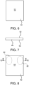
FIG. 6 is a top view of the secondary face material/polishable layer ofFIG. 5 ; -
FIG. 7 is a side view of the polishable layer ofFIG. 5 , before the layer is combined with the green-state structure illustrated inFIGS. 4 and 5 ; -
FIG. 8 is a top view of the multi-component device ofFIG. 3 ; -
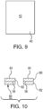
FIG. 9 is a bottom view of the multi-component device ofFIGS. 3 and8 ; -
FIG. 10 is a cross-sectional view of examples of parts removed from the multi-component device ofFIGS. 3 ,8 and9 , taken along line 10-10 ofFIG. 8 ; and -
FIG. 11 is a flow chart for an example of a method of making the parts illustrated inFIG. 10 . - Throughout the drawings, like elements are designated by like reference numerals and other characters. The drawings show non-limiting examples for purposes of illustration and explanation of the present disclosure, and are not drawn to scale.
- The technical problem is solved by the independent claims. The dependent claims cover further specific embodiments of the invention.
- Referring now to the drawings,
FIG. 3 shows an example of a multi-component, combinedstructure 40 constructed in accordance with the present disclosure. Themulti-component structure 40 includes a substrate 42 (an example of a first component) and a polishable layer 44 (an example of a second component). Thesubstrate 42 may be a layer (as illustrated inFIG. 3 ) or may have some other, suitable shape. - If desired, the
multi-component structure 40 may have more than two components. Theperiphery 48 of thepolishable layer 44 is not necessarily coextensive with theperiphery 50 of thesubstrate 42. The present disclosure should not be limited to features shown in the drawings except to the extent such features are recited in the appended claims. - The
substrate 42 is formed of the RB-SiC material 26 illustrated inFIG. 2 . That is, the substrate 42 (FIG. 3 ) includes a fully dense, three-component microstructure including original silicon-carbide particles 22 (FIG. 2 ), reaction-bonded silicon carbide 28, and residual (unreacted)elemental silicon 30. - The
polishable layer 44 is formed of a suitable polishable material and does not include RB-SiC. Thepolishable layer 44 may include chemical-vapor-deposited silicon-carbide (CVD-SiC), single-crystal silicon-carbide (Xtal-SiC), or another suitable material or materials. The material of thepolishable layer 44 may be selected so thatpolishable layer 44 has a good coefficient of thermal expansion (CTE) match to thesubstrate 42 across a wide range of temperatures. According to one aspect of the present disclosure, the difference in CTE between thesubstrate 42 and thepolishable layer 44 is preferably less than 2.0 ppm/°C, and even more preferably less than 0.2 ppm/°C. As used herein, the phrase "a wide range of temperatures" means "a range of temperatures between ambient and the melting point of silicon." Thepolishable layer 44 has apolishable surface 52. If desired, thesurface 52 is polished to an extremely high dimensional accuracy and an extremely low roughness. - The
polishable layer 44 may be formed in a chemical-vapor-deposition process, a single-crystal formation process, or another suitable process. According to one aspect of the present disclosure, the material of thepolishable layer 44 has only one phase. In contrast to thesubstrate 42, thepolishable layer 44 is not formed of a multi-phase material. As a result, it is easier to accurately polish thepolishable surface 52 than it would be to accurately polish a surface of thesubstrate 42. If desired, thepolishable layer 44 is formed and subjected to a suitable polishing process independently of (before or after) the infiltration process by which thesubstrate 42 is formed. - A green-
state structure 60 for use in forming thesubstrate 42 is illustrated inFIGS. 4 and 5 . The green-state structure 60 includes the same porous interconnected material as that of theporous mass 20 shown inFIG. 1 . That is, the green-state structure 60 (FIGS. 4 and 5 ) includes interconnected silicon-carbide particles 22 (FIG. 1 ) andcarbon 24. - The interconnected material of the green-state structure 60 (
FIGS. 4 and 5 ) may be sufficiently cohesive and strong to permit movement and handling without degrading edges and surfaces of the green-state structure 60. The cohesiveness and strength of the interconnected green-state structure 60 may be established during the casting of the silicon-carbide particles 22 (FIG. 1 ) andcarbon 24. - In operation, an
unpolished surface 54 of thepolishable layer 44 and a first surface 62 (also unpolished) of the green-state structure 60 are brought into contact with each other to form thepreform 64 illustrated inFIG. 5 . If desired, the green-state structure 60 may be cast onto thesecond surface 54 of thepolishable layer 44. Then, molten elemental silicon (not illustrated inFIGS. 4 and 5 ) infiltrates into the green-state structure 60, within a vacuum or inert atmosphere, to produce thesubstrate 42. The infiltration process is essentially the same as the one used to produce the RB-SiC material illustrated inFIG. 2 . - According to the present disclosure, however, the infiltration process which completes the formation of the
substrate 42 may be continued such that some of the molten silicon exudes outwardly through the contactingsurface 62, fills interstices between the contactingsurface 62 and theunpolished surface 54 of thepolishable layer 44, comes into contact with theunpolished surface 54, and forms aninterface 56 by reacting with silicon carbide in thepolishable layer 44 to thereby securely bond thesubstrate 42 and thepolishable layer 44 together. - After the infiltration process is completed, that is, after the combined structure 40 (
FIG. 3 ) is formed, individual parts 80 (FIG. 10 ) may be extracted from the combinedstructure 40 using wire electrical-discharge-machining (EDM), spark machining, spark eroding, die sinking, wire burning, wire erosion, or another suitable process. Theparts 80 may be employed as optical mirrors, beam dumps, or other optical devices.Surfaces 81 of the extractedparts 80 are formed of thepolishable layer 44. Thesurfaces 81 face away from thesubstrate 42 and do not contain any RB-SiC. Thesurfaces 81 may be polished after thesubstrate 42 is bonded to thepolishable layer 44. - The
peripheries 82 of the extractedparts 80, where the combinedstructure 40 is machined to extract theparts 80, are designated inFIG. 8 by dotted lines. If desired, the extractedparts 80 may have peripheries and configurations different from the ones illustrated inFIGS. 8 and10 . As noted above, the present disclosure should not be limited to features shown in the drawings except to the extent such features are recited in the appended claims. - The processes described herein may be used to overcome or alleviate difficulties associated with creating an optical quality surface on an RB-SiC material. Such difficulties may be created, at least in part, by the multi-phase nature of RB-SiC. Different Young's moduli, yield strengths, hardnesses, and chemical reactivities of the different phases may make it difficult or impossible to polish RB-SiC to a desired, high degree of smoothness. In contrast to RB-SiC, chemical-vapor-deposited silicon-carbide (CVD-SiC) and single-crystal silicon-carbide (Xtal-SiC) can be polished with extremely high dimensional accuracy and extremely low roughness.
- CVD-SiC, Xtal-SiC, and certain other single-phase, polishable ceramic materials, can be grown only in a limited number of shapes, which makes it difficult or impossible to use such materials in certain optical devices. RB-SiC, in contrast, can be configured in almost any shape through green-state machining, net-shape preform casting of the ceramic, or another suitable process, followed by an infiltration process. By combining a solid piece of single-phase, easily polishable material, such as CVD-SiC or Xtal-SiC, with a body of RB-SiC, one or more extremely high-quality mirrors 81 with independently shaped support structures can be produced.
- Moreover, it may difficult or impossible to form a high-quality mirror, with properties equivalent to the
polishable layer 44 of the present disclosure, by depositing a CVD-SiC coating on a RB-SiC substrate. Such a directly deposited coating may be too thin, irregular, or internally stressed to be acceptable. Moreover, additional operational time may be required to level the directly deposited coating, and production yield may be adversely impacted if the irregularity of the coating were to cause the polishing operation to break through the coated surface to the underlying RB-SiC material. Additionally, a directdeposition process may result in the formation of unwanted deposits on one or more nonoptical surfaces. - The present disclosure overcomes many or all of these potential challenges by bonding a bulk piece of a material other than RB-SiC, such as CVD-SiC or Xtal-SiC, to an RB-
SiC body 42 during an RB-SiC infiltration process. By casting a green-body ceramic 60 on a piece of CVD-SiC or Xtal-SiC, the crystalline SiC in thepolishable layer 44 can bond to the ceramic RB-SiC during the infiltration process. If desired, the processes described above may be combined with RB-SiC to RB-SiC bonding methods to create more complex geometries like internal cooling channels (not illustrated). - If desired, the present disclosure may be implemented in connection with other ceramic substrates that are compatible with a reaction-bonding infiltration process. The RB-
SiC substrate 42 illustrated inFIG. 3 is a non-limiting example of such ceramic substrates. Thepolishable surface 44 may be formed of any suitable material, other than the multi-phase material of the substrate, including, but not limited to, aluminum nitride (AlN), diamond, or a single-crystal silicon-carbide of any suitable allotrope or crystallographic orientation. - A method of producing the
parts 80 illustrated inFIG. 10 is illustrated inFIG. 11 . The method includes astep 100 of providing a green-state structure 60 and apolishable layer 44, and asubsequent step 102 of infiltrating elemental silicon into and through the green-state structure 60. In the illustrated method, the green-state structure 60 is preferably a porous mass of interconnected silicon-carbide plus carbon and is configured to receive molten elemental silicon by capillary action during the infiltratingstep 102. - As a result of the infiltrating
step 102, a substrate of fully dense, two-phase ceramic material is formed in place of the green-state structure, and an interface is formed by a reaction between the silicon and the material of the polishable layer, which interface bonds the substrate and the polishable layer together. - The processes described herein may be employed to produce a thick, uniform, face sheet of silicon carbide (or another suitable, polishable material) without any chemical-vapor-deposition occurring outside of optical area(s). Additionally, the processes described herein may have a relatively small number of process steps, and may be performed in an efficient and uncomplicated manner
Claims (20)
- A multi-component device, comprising:- a ceramic substrate formed of a first material;- a polishable layer formed of a second material different from the first material, and wherein the polishable layer and the ceramic substrate have well-matched coefficients of thermal expansion (CTEs); and- an interface bonding the ceramic substrate and the polishable layer together, the interface being formed by infiltrating elemental silicon.
- The multi-component device of claim 1, wherein the ceramic substrate includes reaction-bonded silicon-carbide (RB-SiC).
- The multi-component device of claim 1, wherein the polishable layer includes chemical-vapor-deposited silicon carbide (CVD-SiC).
- The multi-component device of claim 1, wherein the polishable layer includes single-crystal silicon-carbide (Xtal-SiC).
- An optical device, comprising the multi-component device of claim 1, wherein the polishable layer has a polishable surface facing away from the ceramic substrate.
- The optical device of claim 5, wherein the polishable surface is polished to reflect light.
- The optical device of claim 5, wherein the optical device includes a light-absorbing beam dump.
- The optical device of claim 5, wherein the ceramic substrate includes reaction-bonded silicon-carbide (RB-SiC).
- The optical device of claim 8, wherein the polishable layer includes chemical-vapor-deposited silicon carbide (CVD-SiC).
- The optical device of claim 8, wherein the polishable layer includes single-crystal silicon-carbide (Xtal-SiC).
- A method of making a multi-component device, comprising:- providing a green-state structure and a polishable layer, wherein the green-state structure includes a porous mass of interconnected silicon carbide; and- subsequently, infiltrating elemental silicon into and through the green-state structure to form a substrate of a multi-phase ceramic material from the green-state structure, and to bond the substrate and the polishable layer together, and wherein the polishable layer and the ceramic substrate have well-matched coefficients of thermal expansion (CTEs).
- The method of claim 11, wherein the ceramic material of the substrate includes reaction-bonded silicon-carbide (RB-SiC).
- The method of claim 11 wherein the polishable layer includes chemical-vapor-deposited silicon-carbide (CVD-SiC).
- The method of claim 11 wherein the polishable layer includes single-crystal silicon-carbide (Xtal-SiC).
- The method of claim 11, wherein the polishable layer does not include reaction-bonded silicon-carbide (RB-SiC).
- The method of claim 11, wherein the multi-component device includes an optical device, and wherein the method includes extracting the optical device from the bonded substrate and polishable layer.
- The method of claim 16, wherein the substrate includes reaction-bonded silicon-carbide (RB-SiC).
- The method of claim 16 wherein the polishable layer includes chemical-vapor-deposited silicon carbide (CVD-SiC).
- The method of claim 16, wherein the polishable layer includes single-crystal silicon-carbide (Xtal-SiC).
- The method of claim 16, wherein the step of extracting the optical device from the bonded substrate and polishable layer includes wire electrical-discharge-machining (EDM).
Applications Claiming Priority (1)
| Application Number | Priority Date | Filing Date | Title |
|---|---|---|---|
| US18/155,546 US12338187B2 (en) | 2023-01-17 | 2023-01-17 | Multi-component device and method of making a multi-component device |
Publications (1)
| Publication Number | Publication Date |
|---|---|
| EP4403536A1 true EP4403536A1 (en) | 2024-07-24 |
Family
ID=89430530
Family Applications (1)
| Application Number | Title | Priority Date | Filing Date |
|---|---|---|---|
| EP23218687.4A Pending EP4403536A1 (en) | 2023-01-17 | 2023-12-20 | Multi-component device and method of making a multi-component device |
Country Status (2)
| Country | Link |
|---|---|
| US (2) | US12338187B2 (en) |
| EP (1) | EP4403536A1 (en) |
Citations (4)
| Publication number | Priority date | Publication date | Assignee | Title |
|---|---|---|---|---|
| US20110221084A1 (en) * | 2010-03-10 | 2011-09-15 | Trex Enerprises Corp. | Honeycomb composite silicon carbide mirrors and structures |
| US20190369308A1 (en) * | 2018-05-30 | 2019-12-05 | Raytheon Company | Method of Manufacture for a Lightweight, High-Precision Silicon Carbide Mirror Assembly |
| US20210331985A1 (en) | 2020-04-28 | 2021-10-28 | Ii-Vi Delaware, Inc. | Ceramic substate with reaction-bonded silicon carbide having diamond particles |
| US20220227676A1 (en) | 2021-01-19 | 2022-07-21 | ll-VI Delaware, Inc | Silicon carbide body with localized diamond reinforcement |
Family Cites Families (16)
| Publication number | Priority date | Publication date | Assignee | Title |
|---|---|---|---|---|
| JPH05335529A (en) | 1992-05-28 | 1993-12-17 | Fujitsu Ltd | Semiconductor device and manufacturing method thereof |
| US7124753B2 (en) | 1997-04-04 | 2006-10-24 | Chien-Min Sung | Brazed diamond tools and methods for making the same |
| US20050203630A1 (en) | 2000-01-30 | 2005-09-15 | Pope Bill J. | Prosthetic knee joint having at least one diamond articulation surface |
| US20140109756A1 (en) | 2000-07-21 | 2014-04-24 | Michael K. Aghjanian | Composite materials and methods for making same |
| US6551176B1 (en) | 2000-10-05 | 2003-04-22 | Applied Materials, Inc. | Pad conditioning disk |
| US7300338B2 (en) | 2005-09-22 | 2007-11-27 | Abrasive Technology, Inc. | CMP diamond conditioning disk |
| DE102007063517B3 (en) | 2007-12-21 | 2009-01-22 | Fraunhofer-Gesellschaft zur Förderung der angewandten Forschung e.V. | Manufacturing wear-resistant silicon carbide- or carbon component, coats substrate with diamond crystals and binder, fires and infiltrates with silicon at high temperature |
| US20120328811A1 (en) | 2011-06-24 | 2012-12-27 | Air Products And Chemicals, Inc. | Epoxy Resin Compositions |
| US9469918B2 (en) | 2014-01-24 | 2016-10-18 | Ii-Vi Incorporated | Substrate including a diamond layer and a composite layer of diamond and silicon carbide, and, optionally, silicon |
| JP5729517B1 (en) | 2014-03-28 | 2015-06-03 | Toto株式会社 | Reaction sintered silicon carbide member |
| WO2016164498A1 (en) | 2015-04-06 | 2016-10-13 | M Cubed Technologies, Inc. | Article having diamond-only contact surfaces |
| DE112017001938T5 (en) | 2016-04-06 | 2019-01-17 | M Cubed Technologies, Inc. | Diamond composite conditioner for a CMP cloth |
| EP3241815B1 (en) | 2016-05-02 | 2019-11-13 | Rolls-Royce High Temperature Composites Inc | Reducing surface nodules in melt-infiltrated ceramic matrix composites |
| DE102018203882A1 (en) | 2018-03-14 | 2019-09-19 | Fraunhofer-Gesellschaft zur Förderung der angewandten Forschung e.V. | Process for the production of hard material particles from SiC-bonded diamond, hard-material particles produced by the process, porous components produced with the hard-material particles and their use |
| CA3107399A1 (en) | 2018-08-20 | 2020-02-27 | Kyocera Fineceramics Precision Gmbh | Additive manufacturing of structural components on the basis of silicon carbide with embedded diamond particles |
| US20230373871A1 (en) | 2022-05-18 | 2023-11-23 | Ii-Vi Delaware, Inc. | Reaction-bonded silicon-carbide with in-situ formed silicon layer for optical finishing |
-
2023
- 2023-01-17 US US18/155,546 patent/US12338187B2/en active Active
- 2023-12-20 EP EP23218687.4A patent/EP4403536A1/en active Pending
-
2025
- 2025-05-27 US US19/218,734 patent/US20250282689A1/en active Pending
Patent Citations (4)
| Publication number | Priority date | Publication date | Assignee | Title |
|---|---|---|---|---|
| US20110221084A1 (en) * | 2010-03-10 | 2011-09-15 | Trex Enerprises Corp. | Honeycomb composite silicon carbide mirrors and structures |
| US20190369308A1 (en) * | 2018-05-30 | 2019-12-05 | Raytheon Company | Method of Manufacture for a Lightweight, High-Precision Silicon Carbide Mirror Assembly |
| US20210331985A1 (en) | 2020-04-28 | 2021-10-28 | Ii-Vi Delaware, Inc. | Ceramic substate with reaction-bonded silicon carbide having diamond particles |
| US20220227676A1 (en) | 2021-01-19 | 2022-07-21 | ll-VI Delaware, Inc | Silicon carbide body with localized diamond reinforcement |
Also Published As
| Publication number | Publication date |
|---|---|
| US20240239715A1 (en) | 2024-07-18 |
| US20250282689A1 (en) | 2025-09-11 |
| US12338187B2 (en) | 2025-06-24 |
Similar Documents
| Publication | Publication Date | Title |
|---|---|---|
| US8568650B2 (en) | Silicon carbide matrix composite material, process for producing the same and process for producing part of silicon carbide matrix composite material | |
| US5151107A (en) | Cemented and cemented/sintered superabrasive polycrystalline bodies and methods of manufacture thereof | |
| US4875616A (en) | Method of producing a high temperature, high strength bond between a ceramic shape and metal shape | |
| US5011509A (en) | Composite compact with a more thermally stable cutting edge and method of manufacturing the same | |
| JP4939232B2 (en) | Composite ceramic body, method for producing the same, microchemical chip, and reformer | |
| US4496372A (en) | Abrasive bodies | |
| EP0362594A1 (en) | Joining of silicon carbide parts by polishing and hot isostatic pressing | |
| SE445839B (en) | POLYCRYSTALLINE DIAMOND BODY AND PROCEDURE FOR ITS PREPARATION | |
| EP4279470A1 (en) | Reaction-bonded silicon-carbide with in-situ formed silicon layer for optical finishing | |
| KR20030059307A (en) | Abrasive diamond composite and method of making thereof | |
| US20120285100A1 (en) | Pdc made with low melting point catalyst | |
| KR20020073328A (en) | Silicon carbide composites and methods for making same | |
| US20030027706A1 (en) | Ceramic sintered bodies and a method of producing the same | |
| US6332568B1 (en) | Wafer scale micromachine assembly method | |
| US20220410269A1 (en) | Method for laser beam additive manufacturing of a mechanical part with technical and/or decorative function and mechanical part with technical and/or decorative function | |
| US12338187B2 (en) | Multi-component device and method of making a multi-component device | |
| JP4718397B2 (en) | Manufacturing method of vacuum suction device | |
| JP3981538B2 (en) | Silicon holding container and manufacturing method thereof | |
| JP7794958B2 (en) | Parts manufactured using an infiltration process, devices including the parts, and infiltration processes for manufacturing the parts | |
| Li et al. | Manufacturing silicon carbide microrotors by reactive hot isostatic pressing within micromachined silicon molds | |
| Itoh et al. | Silicon-carbide microfabrication by silicon lost molding for glass-press molds | |
| JP2512942B2 (en) | Manufacturing method of tough ceramic material for gas turbine | |
| JP3893001B2 (en) | Method for forming silicon carbide fine parts | |
| AU9115191A (en) | Composite monolithic lap and a method of making the same | |
| JP2748494B2 (en) | Composite method of ceramics |
Legal Events
| Date | Code | Title | Description |
|---|---|---|---|
| PUAI | Public reference made under article 153(3) epc to a published international application that has entered the european phase |
Free format text: ORIGINAL CODE: 0009012 |
|
| STAA | Information on the status of an ep patent application or granted ep patent |
Free format text: STATUS: THE APPLICATION HAS BEEN PUBLISHED |
|
| AK | Designated contracting states |
Kind code of ref document: A1 Designated state(s): AL AT BE BG CH CY CZ DE DK EE ES FI FR GB GR HR HU IE IS IT LI LT LU LV MC ME MK MT NL NO PL PT RO RS SE SI SK SM TR |
|
| P01 | Opt-out of the competence of the unified patent court (upc) registered |
Free format text: CASE NUMBER: APP_44780/2024 Effective date: 20240801 |
|
| STAA | Information on the status of an ep patent application or granted ep patent |
Free format text: STATUS: REQUEST FOR EXAMINATION WAS MADE |
|
| 17P | Request for examination filed |
Effective date: 20250123 |