EP4401421A1 - Charging case - Google Patents
Charging case Download PDFInfo
- Publication number
- EP4401421A1 EP4401421A1 EP23759284.5A EP23759284A EP4401421A1 EP 4401421 A1 EP4401421 A1 EP 4401421A1 EP 23759284 A EP23759284 A EP 23759284A EP 4401421 A1 EP4401421 A1 EP 4401421A1
- Authority
- EP
- European Patent Office
- Prior art keywords
- region
- profiling
- side edge
- projection
- box body
- Prior art date
- Legal status (The legal status is an assumption and is not a legal conclusion. Google has not performed a legal analysis and makes no representation as to the accuracy of the status listed.)
- Pending
Links
Images










Classifications
-
- H—ELECTRICITY
- H04—ELECTRIC COMMUNICATION TECHNIQUE
- H04R—LOUDSPEAKERS, MICROPHONES, GRAMOPHONE PICK-UPS OR LIKE ACOUSTIC ELECTROMECHANICAL TRANSDUCERS; ELECTRIC HEARING AIDS; PUBLIC ADDRESS SYSTEMS
- H04R1/00—Details of transducers, loudspeakers or microphones
- H04R1/10—Earpieces; Attachments therefor ; Earphones; Monophonic headphones
-
- H—ELECTRICITY
- H04—ELECTRIC COMMUNICATION TECHNIQUE
- H04R—LOUDSPEAKERS, MICROPHONES, GRAMOPHONE PICK-UPS OR LIKE ACOUSTIC ELECTROMECHANICAL TRANSDUCERS; ELECTRIC HEARING AIDS; PUBLIC ADDRESS SYSTEMS
- H04R1/00—Details of transducers, loudspeakers or microphones
- H04R1/10—Earpieces; Attachments therefor ; Earphones; Monophonic headphones
- H04R1/1025—Accumulators specially adapted for earpieces; Arrangements specially adapted for charging thereof
-
- H—ELECTRICITY
- H02—GENERATION; CONVERSION OR DISTRIBUTION OF ELECTRIC POWER
- H02J—ELECTRIC POWER NETWORKS; CIRCUIT ARRANGEMENTS OR SYSTEMS FOR SUPPLYING OR DISTRIBUTING ELECTRIC POWER; SYSTEMS FOR STORING ELECTRIC ENERGY
- H02J7/00—Circuit arrangements for charging or discharging batteries or for supplying loads from batteries
- H02J7/60—Circuit arrangements for charging or discharging batteries or for supplying loads from batteries including safety or protection arrangements
- H02J7/685—Circuit arrangements for charging or discharging batteries or for supplying loads from batteries including safety or protection arrangements using connection detecting circuits
-
- H—ELECTRICITY
- H02—GENERATION; CONVERSION OR DISTRIBUTION OF ELECTRIC POWER
- H02J—ELECTRIC POWER NETWORKS; CIRCUIT ARRANGEMENTS OR SYSTEMS FOR SUPPLYING OR DISTRIBUTING ELECTRIC POWER; SYSTEMS FOR STORING ELECTRIC ENERGY
- H02J7/00—Circuit arrangements for charging or discharging batteries or for supplying loads from batteries
- H02J7/70—Circuit arrangements for charging or discharging batteries or for supplying loads from batteries characterised by the mechanical construction
- H02J7/731—Circuit arrangements for charging or discharging batteries or for supplying loads from batteries characterised by the mechanical construction specially adapted for holding portable devices containing batteries
-
- H—ELECTRICITY
- H02—GENERATION; CONVERSION OR DISTRIBUTION OF ELECTRIC POWER
- H02J—ELECTRIC POWER NETWORKS; CIRCUIT ARRANGEMENTS OR SYSTEMS FOR SUPPLYING OR DISTRIBUTING ELECTRIC POWER; SYSTEMS FOR STORING ELECTRIC ENERGY
- H02J7/00—Circuit arrangements for charging or discharging batteries or for supplying loads from batteries
- H02J7/80—Circuit arrangements for charging or discharging batteries or for supplying loads from batteries including monitoring or indicating arrangements
- H02J7/82—Control of state of charge [SOC]
-
- H—ELECTRICITY
- H04—ELECTRIC COMMUNICATION TECHNIQUE
- H04R—LOUDSPEAKERS, MICROPHONES, GRAMOPHONE PICK-UPS OR LIKE ACOUSTIC ELECTROMECHANICAL TRANSDUCERS; ELECTRIC HEARING AIDS; PUBLIC ADDRESS SYSTEMS
- H04R1/00—Details of transducers, loudspeakers or microphones
- H04R1/10—Earpieces; Attachments therefor ; Earphones; Monophonic headphones
- H04R1/1091—Details not provided for in groups H04R1/1008 - H04R1/1083
-
- H—ELECTRICITY
- H04—ELECTRIC COMMUNICATION TECHNIQUE
- H04R—LOUDSPEAKERS, MICROPHONES, GRAMOPHONE PICK-UPS OR LIKE ACOUSTIC ELECTROMECHANICAL TRANSDUCERS; ELECTRIC HEARING AIDS; PUBLIC ADDRESS SYSTEMS
- H04R3/00—Circuits for transducers
-
- H—ELECTRICITY
- H04—ELECTRIC COMMUNICATION TECHNIQUE
- H04R—LOUDSPEAKERS, MICROPHONES, GRAMOPHONE PICK-UPS OR LIKE ACOUSTIC ELECTROMECHANICAL TRANSDUCERS; ELECTRIC HEARING AIDS; PUBLIC ADDRESS SYSTEMS
- H04R1/00—Details of transducers, loudspeakers or microphones
- H04R1/10—Earpieces; Attachments therefor ; Earphones; Monophonic headphones
- H04R1/1008—Earpieces of the supra-aural or circum-aural type
Definitions
- the present disclosure relates to a technical field of sound generation device, and in particular, to a charging box.
- Earphones have been widely used in people's daily life, and the earphones can be used in conjunction with cell phones, computers, and other electronic devices to provide users with an auditory feast.
- the earphones are equipped with a charging box that is compatible with the earphones, and the charging box is used to charge the earphones.
- the charging box is large in size, which is difficult to carry, and expensive to produce.
- the present disclosure provides a charging box including a first housing assembly.
- the first housing assembly may include a main box body with an opening at one end, and a support plate covering at the open end of the main box body.
- the support plate may be disposed with a profiling groove for accommodating the earphones.
- the support plate may be disposed with a first side edge and a second side edge disposed opposite to each other.
- a depth of a portion of the profiling region close to the first side edge may be greater than the depth of a portion of the profiling region close to the second side edge.
- the depth of the portion of a profiling groove close to the first side edge of the support plate is greater than the depth of the portion of the profiling groove close to the second side edge of the support plate, which can make the profiling groove disposed in an inclined state, and some elements may be disposed on the same horizontal plane where the deepest position of the profiling groove is located and may not overlap with the deepest position of the profiling groove, so as to reduce a total height of other elements and the profiling groove disposed on the charging box in a thickness direction. In this way, a size of the charging box may be reduced, which improves portability and also reduces the production cost.
- first”, “second”, etc. in the present disclosure are used to distinguish different objects and are not used to describe a particular order. Additionally, the terms “comprising”, “including”, and “having”, and any variations thereof, are intended to cover non-exclusive objects. For example, a process, method, system, product, or device including a series of operations or units is not limited to listed operations or units, but also optionally includes operations or units that are not listed, or other operations or units inherent to the process, method, product, or device.
- FIG.1 is a schematic diagram illustrating a structure of an earphone assembly according to the embodiment of the present disclosure.
- an earphone assembly 10 may include earphones 100 and a charging box 200. Specifically, when the charging box 200 is opened, the earphones 100 may be disposed in the charging box 200 to allow the charging box 200 to charge the earphones 100.
- the earphone assembly 10 may include two earphones 100, respectively corresponding to the left ear and the right ear of a person.
- the charging box 200 detects that a power level of the earphone 100 is less than a preset threshold
- the earphone 100 may be charged until the power level is 100%.
- the preset threshold may be 90%.
- the charging box 200 may perform a charging operation on the two earphones 100 when detecting that both the power levels of the two earphones 100 are less than the preset threshold.
- FIG. 2 is a schematic diagram illustrating a structure of the charging box according to the embodiment in FIG. 1 .
- the charging box 200 may include a first housing assembly 210, a second housing assembly 220, a circuit board 230, a battery 240, and a rotary connection assembly 250.
- the first housing assembly 210 may be pivotally connected to the second housing assembly 220.
- the first housing assembly 210 may include a main box body 211 with an opening at one end as an open end of the main box body 211 and a support plate 212 covering over the open end of the main box body 211.
- An accommodation space 214 may be formed between the main box body 211 and the support plate 212, and the circuit board 230, the battery 240, and the rotary connection assembly 250 may be disposed in the accommodation space 214.
- FIG. 3 is a schematic diagram illustrating a first structure of the support plate according to the embodiment in FIG. 2
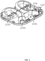
- FIG. 4 is a schematic diagram illustrating a second structure of the support plate according to the embodiment in FIG. 2
- FIG. 5 is a front view of the support plate according to the embodiment in FIG. 2
- FIG. 6 is a schematic diagram illustrating a section of the support plate along an a-a cross-section in FIG.5
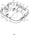
- FIG.7 is a schematic diagram illustrating a structure of the main box body according to the embodiment in FIG. 2 .
- the support plate 212 may be provided with one or more profiling grooves 213 for accommodating the earphones 100.
- the support plate 212 may be provided with a first side edge 21211 and a second side edge 21212 opposite to each other, and a third side edge 21213 and a fourth side edge 21214 opposite to each other.
- the third side edge 21213 and the fourth side edge 21214 may be used to connect the first side edge 21211 and the second side edge 21212.
- the profiling groove 213 may include a first profiling region 2131, a second profiling region 2132, and a third profiling region 2133.
- the third profiling region 2133 may be used for connecting the first profiling region 2131 and the second profiling region 2132.
- the first profiling region 2131 may be disposed close to the first side edge 21211, and the second profiling region 2132 may be disposed close to the second side edge 21212.
- the third profiling region 2133 may include a first boundary 2133A and a second boundary 2133B formed at both ends of an arc segment.
- the third profiling region 2133 may be connected to the second profiling region 2132 through the first boundary 2133A, and connected to the first profiling region 2131 through the second boundary 2133B.
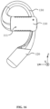
- FIG. 16 is a schematic diagram illustrating a first structure of an earphones according to an embodiment in FIG. 1
- FIG. 17 is a schematic diagram illustrating a second structure of an earphones according to an embodiment in FIG. 1
- the earphones 100 may include a main body portion 110, a battery portion 120, and an elastic connection portion 130.
- the elastic connection portion 130 may be configured to connect the main body portion 110 to the battery portion 120.
- FIG. 16 is a schematic diagram illustrating a first structure of an earphones according to an embodiment in FIG. 1
- FIG. 17 is a schematic diagram illustrating a second structure of an earphones according to an embodiment in FIG. 1 .
- the earphones 100 may include a main body portion 110, a battery portion 120, and an elastic connection portion 130.
- the elastic connection portion 130 may be configured to connect the main body portion 110 to the battery portion 120.
- the main body portion 110 of the earphones 100 may be provided with a first power receiving electrode 141 on a side close to a human ear in a wearing state, and the battery portion 120 may be provided with a second power receiving electrode 142 on the side close to the human ear in the wearing state.
- the elastic connection portion 130 may connect the main body portion 110 to the battery portion 120 to make the earphones 100 curved in a three-dimensional (3D) space when the earphones 100 are in a non-wearing state (i.e., a natural state). That is, the main body portion 110, the battery portion 120, and the elastic connection portion 130 may not be coplanar in the 3D space.
- the main body portion 110 When the earphones 100 are in the wearing state, the main body portion 110 may be configured to contact an anterior side of the ear of a user, and the battery portion 120 and a portion of the elastic connection portion 130 may be configured to be hooked up between a posterior side of the ear of the user and the head of the user.
- the portion of the elastic connection portion 130 may extend from the head toward an outer side of the head and cooperate with the main body portion 110 to provide a compression force on the anterior side of the ear, which in turn realize a cooperation among the main body portion 110, the elastic connection portion 130, and the battery portion 120 to clamp the ear.
- a ratio of a length of the elastic connection portion 130 in a third direction Z to a length of the battery portion 120 in the third direction Z may be greater than or equal to 100%, and preferably, the aforementioned ratio may be greater than or equal to 150%.
- a projection of the battery portion 120 on an X-Y plane may be located within a projection of the elastic connection portion 130 on the X-Y plane.
- a cross-sectional area of at least a part of the battery portion 120 may be greater than a maximum cross-sectional area of the elastic connection portion 130.
- the battery portion 120 may be in a form of a columnar shape, and a ratio between the length and an outer diameter of the battery portion 120 may be less than or equal to 6.
- the first profiling region 2131 may be configured to accommodate the main body portion 110 of the earphones 100
- the second profiling region 2132 may be configured to accommodate the battery portion 120 of the earphones 100
- the third profiling region 2133 may be configured to accommodate the elastic connection portion 130 of the earphones 100.
- the earphones 100 may be disposed inside the charging box 200 along an opposite direction of a first direction X, and the side provided with the first power receiving electrode 141 and the second power receiving electrode 142 of the earphones 100 may be disposed near the profiling grooves 213.
- the depth of a portion of the profiling grooves 213 close to the first side edge 21211 may be greater than the depth of another portion of the profiling grooves 213 close to the second side edge 21212.
- the depth of a portion of the first profiling region 2131 may be less than the depth of the second profiling region 2132, and the depth of a portion of the third profiling region 2133 close to the first side edge 21211 may be greater than the depth of the second profiling region 2132 and greater than the depth of the first profiling region 2131.
- An angle between a line connecting a lowest point A and a highest point B, and a plane parallel to a side of the support plate 212 forming the profiling grooves may be in a range of 10°-60°.
- the lowest point A refers to the lowest point of a surface of one side of the third profiling region 2133 forming the profiling grooves 213 relative to the support plate 212; and the highest point B refers to the highest point of a surface of one side of second profiling region 2132 forming the profiling grooves 213 relative to the support plate 212.
- the highest point B is a connection point of the second power receiving electrode 142 of the earphones 100 and the second profiling region 2132.
- the depth of the second profiling region 2132 for accommodating the battery portion 120 may be less than the depth of the third profiling region 2133 for accommodating the elastic connection portion 130 of the earphones 100, and correspondingly, the depth of the first power receiving electrode 141 of the first profiling region 2131 may be less than the depth of the lowest point A to enable the remaining sweat to flow down to the lowest point A along the first profiling grooves 213. In this way, the remaining sweat may be prevented from contacting the first power receiving electrode 141 on the main body portion 110 and the second power receiving electrode 142 on the battery portion 120 which results in an occurrence of a short circuit.
- the main body portion 110 of the earphones 100 may include a housing 111, a core (not shown), and a main board (not shown).
- the housing 111 may form an accommodation cavity (not shown), the core and the main board may be disposed in the accommodation cavity, and the main board may be disposed with a second microprocessor 112.
- a button (not shown) may be disposed on a side of the housing 111 depart from the elastic connection portion 130, and the button may be electrically connected to the second microprocessor 112.
- the button may be a physical button, a touch button, etc., and specifically may be interaction assemblies such as the physical button, a display, a touch circuit board, etc.
- the button may generate a button trigger signal in response to detecting a signal input by a user, and the second microprocessor 112 may receive the generated button trigger signal and be configured to detect whether an in-box state signal of the earphones 100 is received, then execute a corresponding function based on the button trigger signal and the in-box state signal.
- the second microprocessor 112 may determine that the earphones 100 are placed in the charging box 200 and control the earphones 100 to execute a first function when receiving the button trigger signal generated by the button.
- the second microprocessor 112 may determine that the earphones 100 are not placed in the charging box 200 and control the earphones 100 to execute a second function when receiving the button trigger signal generated by the button.
- the first function may include at least one of coupling the earphones 100 with a communication device or restoring the earphones 100 to its factory settings
- the second function may include at least one of pausing or playing, fast forwarding or rewinding, and switching songs.
- buttons and a cost may be implemented through the same button when the earphones 100 are placed inside and outside the charging box 200, thereby reducing a count of buttons and a cost, and simplifying the structure at the same time.
- the profiling grooves 213 may include two profiling grooves 213 for accommodating the two earphones 100, respectively.
- the two profiling grooves 213 may be disposed in the manner of a mirror image, so that the two earphones 100 disposed in the profiling grooves 213 may also be disposed in mirror image. Therefore, the earphone 100 worn on the left ear by the user is disposed in a left profiling groove 213, and the earphone 100 worn on the right ear by the user is disposed in a right profiling groove 213, which conforms to a habit of the human to take the earphones, and facilitates the user to take the two earphones. Meanwhile, the two earphones 100 may be firmly placed in the charging box 200.
- a spacing L between the two third profiling regions 2133 of the two profiling grooves 213 may gradually decrease and then gradually increase in a direction from the first side edge 21211 to the second side edge 21212.
- the spacing L may be a spacing between adjacent sidewalls of the two third profiling regions 2133 of the two profiling grooves 213.
- the side of the support plate 212 depart from the profiling groove 213 may be further provided with two groups of magnet mounting grooves 21251 and 21252 for placing a first magnet (not shown).
- a first magnet not shown
- the elastic connection portion 130 of the earphones 100 is susceptible to deformation after being worn for a long time period, when the earphones 100 are placed inside the profiling grooves 213, a second magnet inside the earphones 100 may attract to the first magnet, so as to enable the earphones 100 to be fit more closely into the profiling grooves 213, and at the same time minimize a possibility of the earphones 100 from accidentally dropping out of the profiling grooves 213.
- Each group of magnet mounting grooves 21251 may include two first magnets, and the attraction force between the first magnets and the second magnet may be strengthened by disposing the two first magnets.
- the main body portion 110 which is of a greater weight, may be fixed in position, so as to reduce a possibility of the earphones 100 shaking in the profiling grooves 213.
- the side of the support plate 212 depart from the profiling grooves 213 may also be provided with a fastener 2127.
- an inner wall of the main box body 211 may be provided with a snap groove 2113, and the fastener 2127 and the snap groove 2113 may engage with the main box body 211 and the support plate 212 to form the first housing assembly 210.
- a blind hole and a blind post, a magnet, or other manners may also be used for coupling.
- the support plate 212 may include a first flat region 2122 located between the two third profiling regions 2133 of the two profiling grooves 213 and close to the second side edge 21212, and two second flat regions 2123 located on two sides of the two third profiling regions 2133 of the two profiling grooves 213 and close to the third side edge 21213 and the fourth side edge 21214, respectively.
- a projection of the circuit board 230 on a bottom wall of the main box body 211 along the first direction X may be close to a projection of the second side edge 21212 of the support plate 212 on the bottom wall of the main box body 211 along the first direction X.
- the projection of the circuit board 230 on the bottom wall of the main box body 211 along the first direction X may overlap with the projection of the first flat region 2122 on the bottom wall of the main box body 211 along the first direction X.
- the projection of the circuit board 230 on the bottom wall of the main box body 211 along the first direction X may overlap with a projection of at least one of the two second flat regions 2123 on the bottom wall of the main box body 211 along the first direction X.
- FIG.8 is a schematic diagram illustrating a structure of a circuit board in FIG. 2
- FIG. 9 is a schematic diagram illustrating a cooperation between the support plate and the circuit board in FIG. 2
- one side of the circuit board 230 close to the support plate 212 may be provided with a second power supply electrode 232, a first power supply electrode 233, and a detection electrode 234.
- the circuit board 230 may include a first circuit region 2311, a second circuit region 2312, and a connection region 2313.
- a shape of the connection region 2313 may be approximately a ring, which corresponds to an arc transition portion between the second side edge 21212 and the third side edge 21213 on the support plate 212, or corresponds to an arc transition portion between the second side edge 21212 and the fourth side edge 21214 on the support plate 212.
- Two ends of the connection region 2313 may be connected to the first circuit region 2311 and the second circuit region 2312, respectively.
- the second circuit region 2312 may be used to dispose the second power supply electrode 232, and the connection region 2313 may be used to dispose the first power supply electrode 233 and the detection electrode 234.
- connection region 2313 may include a first boundary 2313A and a second boundary 2313B.
- the first boundary 2313A may be parallel to the first side edge 21211 and the second side edge 21212, and the second boundary 2313B may be parallel to the third side edge 21213 and the fourth side edge 21214.
- the connection region 2313 may be connected to the second circuit region 2312 through the first boundary 2313A, and connected to the first circuit region 2311 through the second boundary 2313B.
- the two groups of second circuit regions 2312 and the two groups of connection regions 2313 may be respectively connected to the two ends of the first circuit region 2312 in a direction of the spacing of the third side edges 21213 and the fourth side edges 21214, so as to make the circuit board 230 in a form of a U-shape.
- the circuit board 230 may be symmetrically disposed along a centerline of the first circuit region 2311.
- Two groups of second power supply electrodes 232 respectively disposed at the two groups of the second circuit regions 2312, two groups of first power supply electrodes 233 respectively disposed at the two groups of the connection regions 2313, and two groups of detection electrodes 234 respectively disposed at the two groups of connection regions 2313 may be disposed symmetrically along the centerline of the first circuit region 2311.
- a projection of the first circuit region 2311 on the bottom wall of the main box body 211 along the first direction X may overlap with the projection of the first flat region 2122 on the bottom wall of the main box body 211 along the first direction X.
- the projection of the second circuit region 2312 on the bottom wall of the main box body 211 along the first direction X may overlap with the projection of the second flat region 2123 on the bottom wall of the main box body 211 along the first direction X, and the projection of the second circuit region 2312 on the bottom wall of the main box body 211 may overlap with the projection of the first profiling region 2131 on the bottom wall of the main box body 211.
- connection region 2313 may be connected to the first circuit region 2311 and the second circuit region 2312, and a projection of the connection region 2313 on the bottom wall of the main box body 211 along the first direction X may overlap with the projection of the second profiling region 2132 on the bottom wall of the main box body 211 along the first direction X.
- An overlap area between the connection region 2313 and the second profiling region 2132 may be smaller than an overlap area between the first circuit region 2311 and the first flat region 2122, and the overlap area between the connection region 2313 and the second profiling region 2132 may be smaller than an overlap area between the second circuit region 2312 and the second flat region 2123.
- a large portion of the circuit board 230 may be disposed at a position that does not overlap with the profiling grooves 213, and the circuit board 230 may not overlap the third profiling region 2133, i.e., in a horizontal plane, the circuit board 230 may not overlap with the deepest position of the profiling grooves 213, so as to reduce a total height of the circuit board 230 and the profiling groove 213 disposed on the charging box 200 in a thickness direction of the charging box 200. In this way, a size of the charging box 200 may be reduced, which improves portability, and reduces a production cost simultaneously.
- an overlap area between the projection of the circuit board 230 on the bottom wall of the main box body 211 and a projection of the third profiling region 2133 on the bottom wall of the main box body 211 may be less than 5% of a total projection area of the circuit board 230 on the bottom wall of the main box body 211.
- the overlap area may be 5%, 4%, 3%, 2%, 1%, or 0%, where 0% indicates that the projection of the circuit board 230 on the bottom wall of the main box body 211 and the projection of the third profiling region 2133 on the bottom wall of the main box body 211 are completely non-overlapping.
- the first profiling region 2131 may include a boss 21241 and a charging port 21242 disposed on a side of the boss 21241 to expose the second power supply electrode 232 at the charging port 21242.
- the second profiling region 2132 may be provided with a through hole 21243 to expose the first power supply electrode 233 and the detection electrode 234 at the through hole 21243.
- FIG. 12 is a schematic diagram illustrating a first circuit of a charging box according to some embodiments of the present disclosure.
- the charging box 200 may include a first microprocessor 2314 and a charging circuit 2315 disposed on a circuit board 230.
- the first microprocessor 2314 may be connected to the charging circuit 2315 and the battery 240, and the charging circuit 2315 may be connected to the second power supply electrode 232 and the first power supply electrode 233.
- the second power supply electrode 232 may be a Pogopin, and the first power supply electrode 233 and the detection electrode 234 may be poppet electrodes.
- the detection electrode 234 and the first power supply electrode 233 may be disposed in a V-shape opposite to each other.
- two surfaces of the detection electrode 234 and the first power supply electrode 233 opposite to each other may substantially form a V-shape structure.
- the second power supply electrode 232 may be a charging positive electrode
- the first power supply electrode 233 may be a charging negative electrode.
- the first power receiving electrode 141 may abut against the second power supply electrode 232, and the second power receiving electrode 142 may abut against both the first power supply electrode 233 and the detection electrode 234, so as to make the charging circuit 2315 charge the earphones 100 placed in the charging box 200 through the charging circuit formed by the second power supply electrode 232 and the first power supply electrode 233.
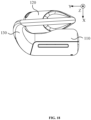
- FIG. 18 is a schematic diagram illustrating a third structure of earphones according to the embodiment in FIG. 1 .
- the main body portion 110 of the earphones 100 may not be at the same level as the battery portion 120.
- the main body portion 110 and a part of the elastic connection portion 130 connected to the main body portion 110 may surround the boss 21241 to make the earphones 100 fit to the profiling grooves 213, and further make it easier for the first power receiving electrode 141 to abut against the second power supply electrode 232.
- the second power receiving electrode 142 may be a strip electrode or a ring electrode such that the earphones 100 may be placed in the profiling grooves 213, and the second power receiving electrode 142 may fully abut against the first power supply electrode 233 and the detection electrode 234.
- the detection electrode 234 and the first power supply electrode 233 disposed opposite to each other in the V shape may better support and fix the battery portion 120 of the earphones 100, thereby preventing the movement of the earphones 100 that causes the second power receiving electrode 142 to be electrically disconnected from the first power supply electrode 233 and/or the detection electrode 234.
- FIG. 13 is a schematic diagram illustrating a second circuit of a charging box according to some embodiments of the present disclosure.
- the charging box 200 may include a detection circuit 23143.
- the detection circuit 23143 may be connected to the first microprocessor 2314 and a connection end of the detection electrode 234.
- the second power receiving electrode 142 may simultaneously abut against the first power supply electrode 233 and the detection electrode 234, so that the detection electrode 234 may be shorted to the first power supply electrode 233 while the first power supply electrode 233 is the charging negative electrode. Therefore, a level of the detection electrode 234 may be pulled down, which in turn produces a level change. When the earphones 100 are not placed in the charging box 200, then the level of the detection electrode 234 may remain unchanged.
- the detection circuit 23143 may generate a detection signal corresponding to the in-box state of the earphones 100 through detecting the level change of the detection electrodes 234, and transmit the detection signal to the first microprocessor 2314 to notify the first microprocessor 2314 of the in-box state of the earphones 100.
- the detection circuit 23143 may include a first sub-detection circuit 231431 and a second sub-detection circuit 231432, which are used for detecting the in-box state of the two earphones 100, respectively.
- the second power receiving electrode 142 of one of the earphones 100 may abut against one of the two groups of detection electrodes 234 and one of the two groups of first power supply electrodes 233.
- the second power receiving electrode 142 of the other of the earphones 100 may abut against the other of the two groups of detection electrodes 234 and the other of the two groups of first power supply electrodes 233.
- the first sub-detection circuit 231431 and the second sub-detection circuit 231432 may perform in-box detections on the two earphones 100 by respectively detecting level changes of a detection electrode 234-1 and a detection electrode 234-2.
- the first sub-detection circuit 231431 may include a resistor R1, a diode D1, and a capacitor C1.
- One end of the resistor R1 may be connected to the first microprocessor 2314 and one end of the capacitor C1, and the other end of the capacitor C1 may be grounded.
- the other end of the resistor R1 may be connected to a connection end of the detection electrode 234-1 and one end of the diode D1, and the other end of the diode D1 may be grounded.
- the second sub-detection circuit 231432 may include a resistor R2, a diode D2, and a capacitor C2.
- One end of the resistor R2 may be connected to the first microprocessor 2314 and one end of the capacitor C2, the other end of the resistor R2 may be connected to the connection end of the detection electrode 234-2 and one end of the diode D2, and the other end of the capacitor C2 may be connected to the other end of the diode D2 and grounded.
- the present embodiment of the charging box 200 may perform the in-box detection by detecting the level change of the detection electrode 234 through the detection circuit 23143. In this way, there may be no need to set up a separate complex detection device or circuit, thereby simplifying a circuit structure of the charging box 200 and reducing the cost.
- the charging box 200 determines that the earphones 100 have been placed in the charging box 200 based on the detection signal generated by the detection circuit 23143, the earphones 100 may be charged by the charging circuit 2315.
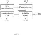
- FIG. 14 is a schematic diagram illustrating a third circuit of a charging box according to some embodiments of the present disclosure.
- the charging box 200 may include a switching circuit 23142 and a communication circuit 23141 disposed on the circuit board 230.
- the switching circuit 23142 may be connected to the charging circuit 2315, the first power supply electrode 233, and the first microprocessor 2314, and the communication circuit 23141 may be connected to the first microprocessor 2314 and the switching circuit 23142.
- the communication circuit 23141 may be a circuit independently disposed on the circuit board 230 or integrated within the first microprocessor 2314.
- the first microprocessor 2314 may control the switching circuit 23142 to make the charging circuit 2315 intermittently connected and disconnected to the first power supply electrode 233.
- the first microprocessor 2314 may be disposed to control the communication circuit 23141 to communicate with the earphones 100 through the first power supply electrode 2333 during a period in which the charging circuit 2315 is disconnected to the first power supply electrode 233, so as to send a power level query signal to the earphones 100.
- the charging circuit 2315 may be intermittently conducted and disconnected to the first power supply electrode 233 at a frequency of 5s -1 , i.e., in one period, a total duration of a time for the first microprocessor 2314 to control the charging circuit 2315 to charge the earphones 100 and a time for the first microprocessor 2314 to control the communication circuit 23141 to communicate with the earphones 100 may be 200 ms.
- the charging circuit 2315 may be disconnected, and the communication circuit 23141 may be controlled to communicate with the earphones 100 for a preset time.
- the time for charging may be 195ms and the time for communication may be 5ms, and this embodiment is not limited herein.
- the first microprocessor 2314 may further control the charging circuit 2315 to be disconnected from the first power supply electrode 233 when a power level of the earphones fed back by the earphones 100 reaches a preset power level threshold, and control the communication circuit 23141 to send a power-off signal through the first power supply electrode 233 to the earphones 100.
- the first microprocessor 2314 may control the communication circuit 23141 to send an in-box state signal, a power level query signal, and a power-off signal to the second microprocessor 112 of the earphones 100.
- the second microprocessor 112 may send remaining power information to the charging box 200 according to the in-box state signal and the power level query signal, and control the earphones 100 to power off according to the power-off signal.
- the earphones 100 may further include a first detection circuit for detecting the in-box state of the earphones 100 and generate first in-box state information according to the in-box state of the earphones 100.
- the second microprocessor 112 may receive the in-box state signal generated by the detection circuit 23143 and/or the first in-box state information generated by the first detection circuit to determine that the earphones 100 are placed in the charging box 200.
- the second microprocessor 112 may determine that the earphones 100 are placed in the charging box 200.
- the second microprocessor 112 may determine that the earphones 100 are placed in the charging box 200 and determines that the charging box 200 is faulty, so as to generate a failure reminder signal.
- FIG. 15 is a schematic diagram illustrating a switching circuit according to an embodiment in FIG. 14 .
- the switching circuit 23142 may include a P-channel Metal Oxide Semiconductor(PMOS) tube Q1, an N-channel metal oxide semiconductor(NMOS) tube Q2, a resistor R3, a resistor R4, a resistor R5, a resistor R6, and a diode D3.
- PMOS Metal Oxide Semiconductor
- NMOS N-channel metal oxide semiconductor
- a source electrode of the PMOS tube Q1 may be connected to the charging circuit 2315 and one end of the resistor R3 to receive an output signal 5V_earbuds of the charging circuit 2315.
- a drain electrode of the PMOS tube Q1 may be connected to a connection end of the first power supply electrode 233, specifically, connected to a first power supply electrode 233-1 and a first power supply electrode 233-2, which correspond to the two groups of first power supply electrodes 233 that abut against the second power receiving electrodes 142 of the two earphones 100, respectively.
- a grid electrode of the PMOS tube Q1 may be connected to a drain electrode of the NMOS tube Q2 and the other end of the resistor R3.
- a source electrode of the NMOS tube Q2 may be connected to one end of the resistor R5, and the other end of the resistor R5 may be grounded.
- a grid electrode of the NMOS tube Q2 may be connected to the first microprocessor 2314 and one end of the resistor R4 to receive a control signal 5V_output_control output by the first microprocessor 2314, and the other end of the resistor R4 may be grounded.
- One end of the resistor R6 may be connected to the first microprocessor 2314 to receive a pull-up voltage One_wire_power output by the first microprocessor 2314, and the other end of the resistor R6 may be connected to a positive pole of the diode D3 and a data receiving end RX of the communication circuit 23141.
- a negative pole of the diode D3 may be connected to a data sending end TX of the communication circuit 23141.
- the charging box 200 may further include an anti-backflow device Q3.
- the anti-backflow device Q3 may be disposed between the connection end of the switching circuit 23142 and the first power supply electrode 233 and the communication circuit 23141 for preventing a charging current on the charging circuit from flowing backwards to the communication circuit 23141.
- a source electrode of the anti-backflow device Q3 may be connected to the other end of the resistor R6, and a drain electrode of the anti-backflow device Q3 may be connected to the connection end of the two groups of first power supply electrodes 233 (i.e., the first power supply electrode 233-1 and the first power supply electrode 233-2).
- a grid electrode of the anti-backflow device Q3 may be connected to the first microprocessor 2314 to output a reference voltage of 3.3V.
- the switching circuit 23142 may further include a resistor R7, a diode D4, and a diode D5.
- the resistor R7 may be used to prevent a short circuit.
- the diode D4 and the diode D5 may be used to prevent a static electricity.
- One end of the resistor R7 may be connected to the drain electrode of the anti-backflow device Q3 and one end of the diode D5.
- the other end of the resistor R7 and the other end of the diode D5 may be grounded, respectively.
- One end of the diode D4 may be connected to the drain electrode of the PMOS tube Q1, and the other end of the diode D4 may be grounded.
- the switching circuit 23142 of the present embodiment may control the PMOS tube Q1 to conduct or cut off by receiving the control signal 5V output control output by the first microprocessor 2314, thereby achieving time-sharing multiplexing for charging and communication, which simplifies the circuit.
- the second housing assembly 220 may include a third housing 221 and a fourth housing 222.
- the third housing 221 may be sleeved outside the fourth housing 222 to form the second housing assembly 220.
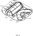
- FIG. 10 is a schematic diagram illustrating a structure of a fourth housing according to an embodiment in FIG. 2 .
- the fourth housing 222 may include a main board 2221, a first accommodation groove 2222, and a second accommodation groove 2223.
- the first accommodation groove 2222 and the second accommodation groove 2223 may be disposed on a side of the main board 2221 depart from the third housing 221.
- a projection of the first accommodation groove 2222 on the support plate 212 may overlap with the first profiling region 2131 and a portion of the third profiling region 2133, and a projection of the second accommodation groove 2223 on the support plate 212 may overlap with the second profiling region 2132 and a portion of the third profiling region 2133.
- the earphones 100 When the earphones 100 are placed in the profiling grooves 213, and the second housing assembly 220 covers over the first housing assembly 210, a part of the main body portion 110 of the earphones 100 that is exposed at the profiling grooves 213 may abut against the first accommodation groove 2222. A portion of the battery portion 120 of the earphones 100 that is exposed at the profiling grooves 213 may abut against the second accommodation groove 2223. In this way, the earphones 100 may be fixed.
- the charging box 200 may include a Hall sensor 2316.
- the Hall sensor 2316 may be electrically connected to the first microprocessor 2314.
- the Hall sensor 2316 may include the first Hall sensor and the second Hall sensor.
- a distance between the first Hall sensor and the second Hall sensor may change, so as to generate a rising edge signal or a falling edge signal that is transmitted to the first microprocessor 2314 to notify the first microprocessor 2314 information about the charging box 200 being open or closed.
- the charging box 200 may further include a light-emitting diode (LED) 2317 disposed on the circuit board 230.
- the LED 2317 may be connected to the first microprocessor 2314.
- the side of the circuit board 230 close to the support plate 212 may further be provided with a first light guide 236 and a second light guide 237.
- the first housing assembly 210 and the second housing assembly 220 may form an outer housing of the charging box 200.
- the charging box 200 may further include an earphone power level indicator 2128 disposed inside the outer housing, and a charging box power level indicator 2115 visible from an outside of the outer housing for displaying information of the earphones 100 placed inside the charging box 200 and information of the charging box 200 itself, respectively.
- the earphone power level indicator 2128 may be disposed on the support plate 212, specifically disposed in the first flat region 2122, which is visible when the second housing assembly 220 is opened relative to the first housing assembly 210.
- the first light guide 236 may be used to guide light generated by the LED 2317 to the earphone power level indicator 2128 to display information corresponding to the earphones 100 (e.g., the power level or pairing of the earphones 100) by displaying different colors.
- the first microprocessor 2314 may further select a relatively small power level from the power levels fed back from the two earphones 100, and control the earphone power level indicator 2128 to display a light of a color corresponding to the selected power level.
- the main box body 211 may be further provided with the charging box power level indicator 2115, and the second light guide 237 may be used to guide the light generated by the LED 2317 to the charging box power level indicator 2115, so as to make the charging box power level indicator 2115 display information corresponding to the charging box 200 (e.g., the power level of the charging box 200) by displaying different colors.
- the second light guide 237 may be used to guide the light generated by the LED 2317 to the charging box power level indicator 2115, so as to make the charging box power level indicator 2115 display information corresponding to the charging box 200 (e.g., the power level of the charging box 200) by displaying different colors.
- LEDs 2317 there may be five groups of LEDs 2317, namely, a first LED, a second LED, a third LED, a fourth LED, and a fifth LED, which produce green light, green light, orange light, orange light, and white light, respectively.
- the first LED, the third LED, and the fifth LED may be used to display the information of the earphones 100, and the second LED and the fourth LED may be used to display the information of the charging box 200.
- the first microprocessor 2314 may control the first LED, the third LED, or the fifth LED to produce green, orange, or white light based on the power level obtained from power level query information sent to the earphones 100 through the communication circuit 23141.
- the first microprocessor 2314 may control the third LED to be long-lighted, and when the lowest power level of the two earphones 100 is greater than 30%, the first microprocessor 2314 may control the first LED to be long-lighted.
- the first microprocessor 2314 may control the first LED or the third LED to be long-lighted for 5 s according to a difference in the detected power level of the earphones 100.
- the earphones 100 may enter a pairing state.
- the first microprocessor 2314 may control the fifth LED to blink for 3 minutes. If the pairing is successful during the 3 minutes, the first microprocessor 2314 may control the fifth LED to be long-lighted for 5 s. If the pairing fails during the 3 minutes, the first microprocessor 2314 may control the fifth LED to be off.
- the first microprocessor 2314 may obtain a remaining power level of the charging box 200 by detecting the power level of the battery 240.
- the first microprocessor 2314 may control the second LED to be lighted
- the first microprocessor 2314 may control the fourth LED to be lighted.
- the first microprocessor 2314 may control the second LED or the fourth LED to be long-lighted for 5 s according to the difference of the detected power level of the battery 240.
- the side of the circuit board 230 near the support plate 212 may also be provided with a charging interface 235.
- the main box body 211 may also be provided with a through hole 2112.
- the charging interface 235 may be snapped at the through hole 2112 so as to expose the charging interface 235 at the main box body 211.
- the charging box 200 may be connected to an external power source through the charging interface 235 to enable charging for the charging box 200.
- the charging interface 235 may be connected to the charging circuit 2315 to further charge the battery 240 through the charging circuit 2315.
- the charging circuit 2315 may be a charging management chip with functions of step-down charging and step-up discharging.
- the charging circuit 2315 may utilize the step-down charging function to receive an input voltage to charge the battery 240.
- the charging circuit 2315 may utilize the step-up discharging function to raise the voltage output by the battery 240 to the charging voltage of the earphones 100 to charge the earphones 100.
- the charging circuit 2315 may include a step-down charging circuit and a step-up discharging circuit, and the charging of the charging box 200 as well as the earphones 100 may be realized by the corresponding circuit.
- the bottom wall of the main box body 211 may be disposed with one or more positioning blocks 2119.
- the positioning blocks 2119 may be rightangled blocks, and the four positioning blocks 2119 may be symmetrically disposed with each other to form a cuboid for disposing and fixing a position of the battery 240.
- the bottom wall of the main box body 211 may be further provided with a first mounting hole 2117, a second mounting hole 2116, and a third mounting hole 2118. Projections of first mounting hole 2117 and the second mounting hole 2116 on the bottom wall of the main box body 211 may be close to the projection of the first side edge 21211 of the support plate 212 on the bottom wall of the main box body 211, and a projection of the third mounting hole 2118 on the bottom wall of the main box body 211 may be close to the projection of the second side edge 21212 of the support plate 212 on the bottom wall of the main box body 211.
- the side of the circuit board 230 close to the support plate 212 may also be provided with a first screw hole 2381, a second screw hole 2382, and a third screw hole 2383.
- the first screw hole 2381 and the second screw hole 2382 may be disposed in the second circuit region 2312 and close to the first charging electrode 232, respectively.
- the third screw hole 2383 may be disposed in the first circuit region 2311, and a projection of the third screw hole 2383 on the first circuit region 2311 may overlap with a projection of the second light guide 237 on the circuit board 230.
- the circuit board 230 may be disposed on the battery 240, and screwed into the first mounting hole 2117 and the first screw hole 2381, the second mounting hole 2116 and the second screw hole 2382, the third mounting hole 2118 and the third screw hole 2383, respectively. In this way, the circuit board 230 may be fixed in the accommodation space 214. Specifically, the side of the circuit board 230 depart from the support plate 212 may abut against the battery 240 to fix the battery 240.
- the first housing assembly 210 may be rotationally connected and the second housing assembly 220 through the rotary connection assembly 250.
- FIG. 11 is a schematic diagram of the structure according to an embodiment of the rotary connection assembly in FIG. 2 .
- the rotary connection assembly 250 may include a connection main board 251 and a rotary connection plate 252 rotationally connected to each other.
- a mounting groove 254 may be formed on a side of the connection main board 251 near the support plate 212, and the rotary connection plate 252 may be disposed in the mounting groove 254.
- a first boss 2511 and a second boss 2512 may be formed on opposing sides of the connection main board 251, and a third boss 2513 may be formed on a third side adjacent to the two sides.
- the first boss 2511 may be disposed with a first mounting hole (not shown)
- the second boss 2512 may be disposed with a second mounting hole (not shown)
- the third boss 2513 may be disposed with a third mounting hole (not shown).
- a side wall of the main box body 211 adjacent to the first side edge 21211 of the support plate 212 may be formed with an opening 2111.
- the main box body 211 may further include a mounting base 2114 disposed on an inner wall of the side wall where the opening 2111 is formed, and the mounting base 2114 may include a support seat and three screw holes.
- the connection main board 251 may be disposed at the opening 2111, the first mounting hole may be fixed with one of the screw holes of the mounting base 2114 by a first screw 2531.
- the second mounting hole may be fixed with another of the screw holes of the mounting base 2114 through a second screw 2532.
- the third mounting hole may be fixed with the last of the screw holes of the mounting base 2114 through a third screw 2533.
- the rotary connection plate 252 may be fixedly connected to the second housing assembly 220 through screws and screw holes, blind holes and blind posts, or magnets.
- the charging box 200 may drive the second housing assembly 220 to rotate by rotary connection plate 252 so that the second housing assembly 220 may be opened relative to the first housing assembly 210.
- a rotation angle of the first housing assembly 210 relative to the second housing assembly 220 may be in a range of 0°-90°, and when the second housing assembly 220 covers over the first housing assembly 210, the angle between the second housing assembly 220 and the first housing assembly 210 may be 0°. When the second housing assembly 220 is fully open relative to the first housing assembly 210, the angle between the second housing assembly 220 and the first housing assembly 210 may be 90°.
- the rotary connection plate 252 may drive the second housing assembly 220 to autonomously move to a state of being fully opened, and the preset angle may be 45°, 30°, etc.
- a side of the main board 2221 close to the third housing 221 may be provided with a magnet mounting groove 2225.
- the magnet mounting groove 2225 may be disposed close to a side of the main plate 2221 adjacent to the second side edge 21212 of the support plate 212 for mounting and disposing a third magnet (not shown in the figure).
- the side of the support plate 212 depart from the profiling grooves 213 may also be provided with a magnet mounting groove 21253.
- the magnet mounting groove 21253 may be disposed close to the second side edge 21212 for mounting and disposing a fourth magnet (not shown).
- the third magnet and the fourth magnet may attract each other so as to maintain an unchanged position of the second housing assembly 220 relative to the first housing assembly 210, which improves a closing reliability of the charging box 200 simultaneously.
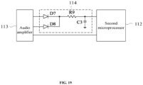
- FIG. 19 is a schematic diagram illustrating a circuit of earphones according to the embodiment of the present disclosure.
- the earphones 100 may include an electrostatic protection circuit 114 and an audio amplifier 113.
- the audio amplifier 113 may be connected to the second microprocessor 112, and the electrostatic protection circuit 114 may be connected to the second microprocessor 112 and the electrostatic protection circuit 114.
- the electrostatic protection circuit 114 may be used to convert an alternating current (AC) signal output by the audio amplifier 113 into a direct current (DC) signal.
- AC alternating current
- DC direct current
- the second microprocessor 112 may determine that the audio amplifier 113 is working abnormally and may send a reset signal to the audio amplifier 113 to make the audio amplifier 113 reset.
- pins of the I/O port may divide the voltage input to the second microprocessor 112, and a divided voltage may be generated. By detecting the voltage value of the divided voltage and comparing the voltage value of the divided voltage with the threshold voltage, the second microprocessor 112 may determine whether the output voltage of the electrostatic protection circuit 114 is abnormal, thereby determining whether the audio amplifier 113 works abnormally.
- the electrostatic protection circuit 114 may include a resistor R9, a capacitor C3, a diode D7, and a diode D8.
- a positive pole of the diode D7 may be connected to a first output end of the audio amplifier 113
- a positive pole of the diode D8 may be connected to a second output of the audio amplifier 113.
- the positive pole of the diode D7 and the positive pole of the diode D8 may receive two AC signals output by the audio amplifier 113.
- a negative pole of the diode D7 may be connected to a negative pole of the diode D8 and one end of the resistor R9.
- the other end of the resistor R9 may be connected to the I/O port of the second microprocessor 112 and one end of the capacitor C3, and the other end of the capacitor C3 may be grounded.
- the other end of the capacitor C3 and the other end of the resistor R9 may form an output end of the electrostatic protection circuit 114.
- the present embodiment provides the electrostatic protection circuit 114 between the audio amplifier 113 and the second microprocessor 112, and by means of the second microprocessor 112, the voltage detection may be performed on the I/O pins connected to the output end of the electrostatic protection circuit 114, which achieves the detection of the state of the audio amplifier 113, and the circuit structure may be simple.
Landscapes
- Engineering & Computer Science (AREA)
- Physics & Mathematics (AREA)
- Acoustics & Sound (AREA)
- Signal Processing (AREA)
- Power Engineering (AREA)
- Charge And Discharge Circuits For Batteries Or The Like (AREA)
Abstract
Description
- This application claims priority to
Chinese Patent Application No. 202210178137.0, filed on February 25, 2022 - The present disclosure relates to a technical field of sound generation device, and in particular, to a charging box.
- Earphones have been widely used in people's daily life, and the earphones can be used in conjunction with cell phones, computers, and other electronic devices to provide users with an auditory feast. Usually, the earphones are equipped with a charging box that is compatible with the earphones, and the charging box is used to charge the earphones.
- The charging box is large in size, which is difficult to carry, and expensive to produce.
- In view of the above, in order to solve the aforementioned technical problem, the present disclosure provides a charging box including a first housing assembly. The first housing assembly may include a main box body with an opening at one end, and a support plate covering at the open end of the main box body. The support plate may be disposed with a profiling groove for accommodating the earphones.
- The support plate may be disposed with a first side edge and a second side edge disposed opposite to each other. A depth of a portion of the profiling region close to the first side edge may be greater than the depth of a portion of the profiling region close to the second side edge.
- Different from the prior art, in the present disclosure, the depth of the portion of a profiling groove close to the first side edge of the support plate is greater than the depth of the portion of the profiling groove close to the second side edge of the support plate, which can make the profiling groove disposed in an inclined state, and some elements may be disposed on the same horizontal plane where the deepest position of the profiling groove is located and may not overlap with the deepest position of the profiling groove, so as to reduce a total height of other elements and the profiling groove disposed on the charging box in a thickness direction. In this way, a size of the charging box may be reduced, which improves portability and also reduces the production cost.
- To more clearly illustrate the technical solutions of the embodiments of the present disclosure, the drawings need to be used in the embodiments or descriptions of the prior art will be briefly introduced below. Obviously, the drawings in the following description are only some embodiments of the present disclosure. For those of ordinary skill in the art, other drawings may be obtained based on these drawings without creative labor., wherein:
-
FIG. 1 is a schematic diagram illustrating a structure of an earphone assembly according to some embodiments of the present disclosure; -
FIG. 2 is a schematic diagram illustrating a structure of a charging box according to an embodiment inFIG. 1 ; -
FIG. 3 is a schematic diagram illustrating a first structure of a support plate according to an embodiment inFIG. 2 ; -
FIG. 4 is a schematic diagram illustrating a second structure of the support plate according to an embodiment inFIG. 2 ; -
FIG. 5 is a front view of the support plate according to an embodiment inFIG. 2 ; -
FIG.6 is a schematic diagram illustrating a section of the support plate along an A-A cross-section inFIG.5 ; -
FIG. 7 is a schematic diagram illustrating a structure of a main box body according to an embodiment inFIG. 2 ; -
FIG. 8 is a schematic diagram illustrating a structure of a circuit board inFIG. 2 ; -
FIG.9 is a schematic diagram illustrating a cooperation between the support plate and the circuit board inFIG.2 ; -
FIG. 10 is a schematic diagram illustrating a structure of a fourth housing according to an embodiment inFIG. 2 ; -
FIG. 11 is a schematic diagram illustrating a structure of a rotary connection assembly according to an embodiment inFIG. 2 ; -
FIG. 12 is a schematic diagram illustrating a first circuit of a charging box according to some embodiments of the present disclosure; -
FIG. 13 is a schematic diagram illustrating a second circuit of a charging box according to some embodiments of the present disclosure; -
FIG. 14 is a schematic diagram illustrating a third circuit of a charging box according to some embodiments of the present disclosure; -
FIG. 15 is a schematic diagram illustrating a switching circuit according to an embodiment inFIG. 14 ; -
FIG. 16 is a schematic diagram illustrating a first structure of earphones according to an embodiment inFIG. 1 ; -
FIG. 17 is a schematic diagram illustrating a second structure of earphones according to an embodiment inFIG. 1 ; -
FIG. 18 is a schematic diagram illustrating a third structure of earphones according to an embodiment inFIG. 1 ; and -
FIG. 19 is a schematic diagram illustrating a circuit of earphones according to the embodiment of the present disclosure. - To enable those skilled in the art to better understand the technical solutions of the present disclosure, the charging box disposed herein is described in further detail below in conjunction with the accompanying drawings and specific embodiments. It may be understood that the described embodiments are only a part of the embodiments of the present disclosure, and not all of them. Based on the embodiments of the present disclosure, all other embodiments obtained by those skilled in the art without making creative labor may fall within the scope of protection of the present disclosure.
- The terms "first", "second", etc., in the present disclosure are used to distinguish different objects and are not used to describe a particular order. Additionally, the terms "comprising", "including", and "having", and any variations thereof, are intended to cover non-exclusive objects. For example, a process, method, system, product, or device including a series of operations or units is not limited to listed operations or units, but also optionally includes operations or units that are not listed, or other operations or units inherent to the process, method, product, or device.
- The present disclosure provides a charging assembly. Referring to
FIG.1, FIG.1 is a schematic diagram illustrating a structure of an earphone assembly according to the embodiment of the present disclosure. As shown inFIG.1 , anearphone assembly 10 may includeearphones 100 and acharging box 200. Specifically, when thecharging box 200 is opened, theearphones 100 may be disposed in thecharging box 200 to allow thecharging box 200 to charge theearphones 100. - In some embodiments, the
earphone assembly 10 may include twoearphones 100, respectively corresponding to the left ear and the right ear of a person. When any one of the twoearphones 100 is placed inside thecharging box 200, and thecharging box 200 detects that a power level of theearphone 100 is less than a preset threshold, theearphone 100 may be charged until the power level is 100%. In some embodiments, the preset threshold may be 90%. - Additionally, when the two
earphones 100 are placed in thecharging box 200, thecharging box 200 may perform a charging operation on the twoearphones 100 when detecting that both the power levels of the twoearphones 100 are less than the preset threshold. - In conjunction with
FIG. 1 , further reference may be made toFIG. 2 , which is a schematic diagram illustrating a structure of the charging box according to the embodiment inFIG. 1 . As shown inFIG.2 , thecharging box 200 may include afirst housing assembly 210, asecond housing assembly 220, acircuit board 230, abattery 240, and arotary connection assembly 250. Thefirst housing assembly 210 may be pivotally connected to thesecond housing assembly 220. - In some embodiments, the
first housing assembly 210 may include amain box body 211 with an opening at one end as an open end of themain box body 211 and asupport plate 212 covering over the open end of themain box body 211. Anaccommodation space 214 may be formed between themain box body 211 and thesupport plate 212, and thecircuit board 230, thebattery 240, and therotary connection assembly 250 may be disposed in theaccommodation space 214. - Combined with
FIG.2 , further referring toFIGs. 3-7 ,FIG. 3 is a schematic diagram illustrating a first structure of the support plate according to the embodiment inFIG. 2 ,FIG. 4 is a schematic diagram illustrating a second structure of the support plate according to the embodiment inFIG. 2 ,FIG. 5 is a front view of the support plate according to the embodiment inFIG. 2 ,FIG. 6 is a schematic diagram illustrating a section of the support plate along an a-a cross-section inFIG.5 , andFIG.7 is a schematic diagram illustrating a structure of the main box body according to the embodiment inFIG. 2 . - As shown in
FIG. 3 andFIG. 5 , thesupport plate 212 may be provided with one ormore profiling grooves 213 for accommodating theearphones 100. In some embodiments, thesupport plate 212 may be provided with afirst side edge 21211 and asecond side edge 21212 opposite to each other, and a third side edge 21213 and afourth side edge 21214 opposite to each other. The third side edge 21213 and thefourth side edge 21214 may be used to connect thefirst side edge 21211 and thesecond side edge 21212. - The
profiling groove 213 may include afirst profiling region 2131, asecond profiling region 2132, and athird profiling region 2133. Thethird profiling region 2133 may be used for connecting thefirst profiling region 2131 and thesecond profiling region 2132. Thefirst profiling region 2131 may be disposed close to thefirst side edge 21211, and thesecond profiling region 2132 may be disposed close to thesecond side edge 21212. - The
third profiling region 2133 may include a first boundary 2133A and asecond boundary 2133B formed at both ends of an arc segment. Thethird profiling region 2133 may be connected to thesecond profiling region 2132 through the first boundary 2133A, and connected to thefirst profiling region 2131 through thesecond boundary 2133B. - Further reference may be made to
FIG. 16 andFIG. 17 .FIG. 16 is a schematic diagram illustrating a first structure of an earphones according to an embodiment inFIG. 1 , andFIG. 17 is a schematic diagram illustrating a second structure of an earphones according to an embodiment inFIG. 1 . As shown inFIG. 16 , theearphones 100 may include amain body portion 110, abattery portion 120, and anelastic connection portion 130. Theelastic connection portion 130 may be configured to connect themain body portion 110 to thebattery portion 120. As shown inFIG. 17 , themain body portion 110 of theearphones 100 may be provided with a firstpower receiving electrode 141 on a side close to a human ear in a wearing state, and thebattery portion 120 may be provided with a secondpower receiving electrode 142 on the side close to the human ear in the wearing state. - The
elastic connection portion 130 may connect themain body portion 110 to thebattery portion 120 to make theearphones 100 curved in a three-dimensional (3D) space when theearphones 100 are in a non-wearing state (i.e., a natural state). That is, themain body portion 110, thebattery portion 120, and theelastic connection portion 130 may not be coplanar in the 3D space. When theearphones 100 are in the wearing state, themain body portion 110 may be configured to contact an anterior side of the ear of a user, and thebattery portion 120 and a portion of theelastic connection portion 130 may be configured to be hooked up between a posterior side of the ear of the user and the head of the user. The portion of theelastic connection portion 130 may extend from the head toward an outer side of the head and cooperate with themain body portion 110 to provide a compression force on the anterior side of the ear, which in turn realize a cooperation among themain body portion 110, theelastic connection portion 130, and thebattery portion 120 to clamp the ear. - In some embodiments, a ratio of a length of the
elastic connection portion 130 in a third direction Z to a length of thebattery portion 120 in the third direction Z may be greater than or equal to 100%, and preferably, the aforementioned ratio may be greater than or equal to 150%. A projection of thebattery portion 120 on an X-Y plane may be located within a projection of theelastic connection portion 130 on the X-Y plane. A cross-sectional area of at least a part of thebattery portion 120 may be greater than a maximum cross-sectional area of theelastic connection portion 130. In this embodiment, thebattery portion 120 may be in a form of a columnar shape, and a ratio between the length and an outer diameter of thebattery portion 120 may be less than or equal to 6. - The
first profiling region 2131 may be configured to accommodate themain body portion 110 of theearphones 100, thesecond profiling region 2132 may be configured to accommodate thebattery portion 120 of theearphones 100, and thethird profiling region 2133 may be configured to accommodate theelastic connection portion 130 of theearphones 100. In some embodiments, as shown inFIG. 1 , theearphones 100 may be disposed inside thecharging box 200 along an opposite direction of a first direction X, and the side provided with the firstpower receiving electrode 141 and the secondpower receiving electrode 142 of theearphones 100 may be disposed near theprofiling grooves 213. - As shown in
FIG. 4 andFIG. 6 , the depth of a portion of theprofiling grooves 213 close to thefirst side edge 21211 may be greater than the depth of another portion of theprofiling grooves 213 close to thesecond side edge 21212. The depth of a portion of thefirst profiling region 2131 may be less than the depth of thesecond profiling region 2132, and the depth of a portion of thethird profiling region 2133 close to thefirst side edge 21211 may be greater than the depth of thesecond profiling region 2132 and greater than the depth of thefirst profiling region 2131. - An angle between a line connecting a lowest point A and a highest point B, and a plane parallel to a side of the
support plate 212 forming the profiling grooves may be in a range of 10°-60°. The lowest point A refers to the lowest point of a surface of one side of thethird profiling region 2133 forming theprofiling grooves 213 relative to thesupport plate 212; and the highest point B refers to the highest point of a surface of one side ofsecond profiling region 2132 forming theprofiling grooves 213 relative to thesupport plate 212. Specifically, the highest point B is a connection point of the secondpower receiving electrode 142 of theearphones 100 and thesecond profiling region 2132. - As the user wears the
earphones 100 for a long time period, sweat may remain on theearphones 100. In this embodiment, the depth of thesecond profiling region 2132 for accommodating thebattery portion 120 may be less than the depth of thethird profiling region 2133 for accommodating theelastic connection portion 130 of theearphones 100, and correspondingly, the depth of the firstpower receiving electrode 141 of thefirst profiling region 2131 may be less than the depth of the lowest point A to enable the remaining sweat to flow down to the lowest point A along thefirst profiling grooves 213. In this way, the remaining sweat may be prevented from contacting the firstpower receiving electrode 141 on themain body portion 110 and the secondpower receiving electrode 142 on thebattery portion 120 which results in an occurrence of a short circuit. - As shown in
FIG. 17 , themain body portion 110 of theearphones 100 may include ahousing 111, a core (not shown), and a main board (not shown). Thehousing 111 may form an accommodation cavity (not shown), the core and the main board may be disposed in the accommodation cavity, and the main board may be disposed with asecond microprocessor 112. - In some embodiments, a button (not shown) may be disposed on a side of the
housing 111 depart from theelastic connection portion 130, and the button may be electrically connected to thesecond microprocessor 112. Alternatively, the button may be a physical button, a touch button, etc., and specifically may be interaction assemblies such as the physical button, a display, a touch circuit board, etc. - The button may generate a button trigger signal in response to detecting a signal input by a user, and the
second microprocessor 112 may receive the generated button trigger signal and be configured to detect whether an in-box state signal of theearphones 100 is received, then execute a corresponding function based on the button trigger signal and the in-box state signal. - When detecting the in-box state signal, the
second microprocessor 112 may determine that theearphones 100 are placed in thecharging box 200 and control theearphones 100 to execute a first function when receiving the button trigger signal generated by the button. When failing to detect the in-box state signal, thesecond microprocessor 112 may determine that theearphones 100 are not placed in thecharging box 200 and control theearphones 100 to execute a second function when receiving the button trigger signal generated by the button. - In some embodiments, the first function may include at least one of coupling the
earphones 100 with a communication device or restoring theearphones 100 to its factory settings, and the second function may include at least one of pausing or playing, fast forwarding or rewinding, and switching songs. - In the embodiment, by multiplexing the functions of the button, different functions may be implemented through the same button when the
earphones 100 are placed inside and outside thecharging box 200, thereby reducing a count of buttons and a cost, and simplifying the structure at the same time. - As shown in
FIG. 5 , theprofiling grooves 213 may include two profilinggrooves 213 for accommodating the twoearphones 100, respectively. The twoprofiling grooves 213 may be disposed in the manner of a mirror image, so that the twoearphones 100 disposed in theprofiling grooves 213 may also be disposed in mirror image. Therefore, theearphone 100 worn on the left ear by the user is disposed in aleft profiling groove 213, and theearphone 100 worn on the right ear by the user is disposed in aright profiling groove 213, which conforms to a habit of the human to take the earphones, and facilitates the user to take the two earphones. Meanwhile, the twoearphones 100 may be firmly placed in thecharging box 200. - A spacing L between the two
third profiling regions 2133 of the twoprofiling grooves 213 may gradually decrease and then gradually increase in a direction from thefirst side edge 21211 to thesecond side edge 21212. In some embodiments, the spacing L may be a spacing between adjacent sidewalls of the twothird profiling regions 2133 of the twoprofiling grooves 213. - As shown in
FIG. 4 , the side of thesupport plate 212 depart from theprofiling groove 213 may be further provided with two groups ofmagnet mounting grooves elastic connection portion 130 of theearphones 100 is susceptible to deformation after being worn for a long time period, when theearphones 100 are placed inside theprofiling grooves 213, a second magnet inside theearphones 100 may attract to the first magnet, so as to enable theearphones 100 to be fit more closely into theprofiling grooves 213, and at the same time minimize a possibility of theearphones 100 from accidentally dropping out of theprofiling grooves 213. - Each group of
magnet mounting grooves 21251 may include two first magnets, and the attraction force between the first magnets and the second magnet may be strengthened by disposing the two first magnets. In this way, themain body portion 110, which is of a greater weight, may be fixed in position, so as to reduce a possibility of theearphones 100 shaking in theprofiling grooves 213. - In some embodiments, the side of the
support plate 212 depart from theprofiling grooves 213 may also be provided with afastener 2127. As shown inFIG. 7 , an inner wall of themain box body 211 may be provided with asnap groove 2113, and thefastener 2127 and thesnap groove 2113 may engage with themain box body 211 and thesupport plate 212 to form thefirst housing assembly 210. Alternatively, in other embodiments, a blind hole and a blind post, a magnet, or other manners may also be used for coupling. - As shown in
FIG. 5 , thesupport plate 212 may include a firstflat region 2122 located between the twothird profiling regions 2133 of the twoprofiling grooves 213 and close to thesecond side edge 21212, and two secondflat regions 2123 located on two sides of the twothird profiling regions 2133 of the twoprofiling grooves 213 and close to the third side edge 21213 and thefourth side edge 21214, respectively. - When the
circuit board 230 is disposed in theaccommodation space 214 of thefirst housing assembly 210, a projection of thecircuit board 230 on a bottom wall of themain box body 211 along the first direction X may be close to a projection of thesecond side edge 21212 of thesupport plate 212 on the bottom wall of themain box body 211 along the first direction X. In some embodiments, the projection of thecircuit board 230 on the bottom wall of themain box body 211 along the first direction X may overlap with the projection of the firstflat region 2122 on the bottom wall of themain box body 211 along the first direction X. The projection of thecircuit board 230 on the bottom wall of themain box body 211 along the first direction X may overlap with a projection of at least one of the two secondflat regions 2123 on the bottom wall of themain box body 211 along the first direction X. - Combined with
FIG. 5 , further reference may be made toFIG. 8 andFIG. 9 .FIG.8 is a schematic diagram illustrating a structure of a circuit board inFIG. 2 , andFIG. 9 is a schematic diagram illustrating a cooperation between the support plate and the circuit board inFIG. 2 . As shown inFIG. 8 , one side of thecircuit board 230 close to thesupport plate 212 may be provided with a secondpower supply electrode 232, a firstpower supply electrode 233, and adetection electrode 234. As shown inFIGs. 8 and9 , thecircuit board 230 may include afirst circuit region 2311, asecond circuit region 2312, and aconnection region 2313. - In some embodiments, a shape of the
connection region 2313 may be approximately a ring, which corresponds to an arc transition portion between thesecond side edge 21212 and the third side edge 21213 on thesupport plate 212, or corresponds to an arc transition portion between thesecond side edge 21212 and thefourth side edge 21214 on thesupport plate 212. Two ends of theconnection region 2313 may be connected to thefirst circuit region 2311 and thesecond circuit region 2312, respectively. Thesecond circuit region 2312 may be used to dispose the secondpower supply electrode 232, and theconnection region 2313 may be used to dispose the firstpower supply electrode 233 and thedetection electrode 234. - In some embodiments, the
connection region 2313 may include afirst boundary 2313A and asecond boundary 2313B. Thefirst boundary 2313A may be parallel to thefirst side edge 21211 and thesecond side edge 21212, and thesecond boundary 2313B may be parallel to the third side edge 21213 and thefourth side edge 21214. Theconnection region 2313 may be connected to thesecond circuit region 2312 through thefirst boundary 2313A, and connected to thefirst circuit region 2311 through thesecond boundary 2313B. - In some embodiments, there are two groups of
second circuit regions 2312 and two groups ofconnection regions 2313, the two groups ofsecond circuit regions 2312 and the two groups ofconnection regions 2313 may be respectively connected to the two ends of thefirst circuit region 2312 in a direction of the spacing of the third side edges 21213 and the fourth side edges 21214, so as to make thecircuit board 230 in a form of a U-shape. Thecircuit board 230 may be symmetrically disposed along a centerline of thefirst circuit region 2311. Two groups of secondpower supply electrodes 232 respectively disposed at the two groups of thesecond circuit regions 2312, two groups of firstpower supply electrodes 233 respectively disposed at the two groups of theconnection regions 2313, and two groups ofdetection electrodes 234 respectively disposed at the two groups ofconnection regions 2313 may be disposed symmetrically along the centerline of thefirst circuit region 2311. - In some embodiments, a projection of the
first circuit region 2311 on the bottom wall of themain box body 211 along the first direction X may overlap with the projection of the firstflat region 2122 on the bottom wall of themain box body 211 along the first direction X. - The projection of the
second circuit region 2312 on the bottom wall of themain box body 211 along the first direction X may overlap with the projection of the secondflat region 2123 on the bottom wall of themain box body 211 along the first direction X, and the projection of thesecond circuit region 2312 on the bottom wall of themain box body 211 may overlap with the projection of thefirst profiling region 2131 on the bottom wall of themain box body 211. - The
connection region 2313 may be connected to thefirst circuit region 2311 and thesecond circuit region 2312, and a projection of theconnection region 2313 on the bottom wall of themain box body 211 along the first direction X may overlap with the projection of thesecond profiling region 2132 on the bottom wall of themain box body 211 along the first direction X. - An overlap area between the
connection region 2313 and thesecond profiling region 2132 may be smaller than an overlap area between thefirst circuit region 2311 and the firstflat region 2122, and the overlap area between theconnection region 2313 and thesecond profiling region 2132 may be smaller than an overlap area between thesecond circuit region 2312 and the secondflat region 2123. A large portion of thecircuit board 230 may be disposed at a position that does not overlap with theprofiling grooves 213, and thecircuit board 230 may not overlap thethird profiling region 2133, i.e., in a horizontal plane, thecircuit board 230 may not overlap with the deepest position of theprofiling grooves 213, so as to reduce a total height of thecircuit board 230 and theprofiling groove 213 disposed on thecharging box 200 in a thickness direction of thecharging box 200. In this way, a size of thecharging box 200 may be reduced, which improves portability, and reduces a production cost simultaneously. - In some embodiments, an overlap area between the projection of the
circuit board 230 on the bottom wall of themain box body 211 and a projection of thethird profiling region 2133 on the bottom wall of themain box body 211 may be less than 5% of a total projection area of thecircuit board 230 on the bottom wall of themain box body 211. For example, the overlap area may be 5%, 4%, 3%, 2%, 1%, or 0%, where 0% indicates that the projection of thecircuit board 230 on the bottom wall of themain box body 211 and the projection of thethird profiling region 2133 on the bottom wall of themain box body 211 are completely non-overlapping. - As shown in
FIG. 3 andFIG. 5 , thefirst profiling region 2131 may include aboss 21241 and a chargingport 21242 disposed on a side of theboss 21241 to expose the secondpower supply electrode 232 at the chargingport 21242. Thesecond profiling region 2132 may be provided with a throughhole 21243 to expose the firstpower supply electrode 233 and thedetection electrode 234 at the throughhole 21243. - Further reference may be made to
FIG. 12 , which is a schematic diagram illustrating a first circuit of a charging box according to some embodiments of the present disclosure. As shown inFIG. 12 , thecharging box 200 may include afirst microprocessor 2314 and acharging circuit 2315 disposed on acircuit board 230. Thefirst microprocessor 2314 may be connected to thecharging circuit 2315 and thebattery 240, and thecharging circuit 2315 may be connected to the secondpower supply electrode 232 and the firstpower supply electrode 233. - In some embodiments, the second
power supply electrode 232 may be a Pogopin, and the firstpower supply electrode 233 and thedetection electrode 234 may be poppet electrodes. Thedetection electrode 234 and the firstpower supply electrode 233 may be disposed in a V-shape opposite to each other. For example, two surfaces of thedetection electrode 234 and the firstpower supply electrode 233 opposite to each other may substantially form a V-shape structure. In this embodiment, the secondpower supply electrode 232 may be a charging positive electrode, and the firstpower supply electrode 233 may be a charging negative electrode. - In some embodiments, when the
earphones 100 are placed in theprofiling grooves 213, the firstpower receiving electrode 141 may abut against the secondpower supply electrode 232, and the secondpower receiving electrode 142 may abut against both the firstpower supply electrode 233 and thedetection electrode 234, so as to make thecharging circuit 2315 charge theearphones 100 placed in thecharging box 200 through the charging circuit formed by the secondpower supply electrode 232 and the firstpower supply electrode 233. - Further reference may be made to
FIG. 18 , which is a schematic diagram illustrating a third structure of earphones according to the embodiment inFIG. 1 . As shown inFIG. 18 , themain body portion 110 of theearphones 100 may not be at the same level as thebattery portion 120. When theearphones 100 are placed in theprofiling grooves 213, themain body portion 110 and a part of theelastic connection portion 130 connected to themain body portion 110 may surround theboss 21241 to make theearphones 100 fit to theprofiling grooves 213, and further make it easier for the firstpower receiving electrode 141 to abut against the secondpower supply electrode 232. - In this embodiment, the second
power receiving electrode 142 may be a strip electrode or a ring electrode such that theearphones 100 may be placed in theprofiling grooves 213, and the secondpower receiving electrode 142 may fully abut against the firstpower supply electrode 233 and thedetection electrode 234. At the same time, thedetection electrode 234 and the firstpower supply electrode 233 disposed opposite to each other in the V shape may better support and fix thebattery portion 120 of theearphones 100, thereby preventing the movement of theearphones 100 that causes the secondpower receiving electrode 142 to be electrically disconnected from the firstpower supply electrode 233 and/or thedetection electrode 234. - In this embodiment, before the
charging circuit 2315 charges theearphones 100 placed in thecharging box 200, it needs to detect whether theearphones 100 are placed in thecharging box 200. Further reference may be made toFIG. 13 , which is a schematic diagram illustrating a second circuit of a charging box according to some embodiments of the present disclosure. As shown inFIG.13 , thecharging box 200 may include adetection circuit 23143. Thedetection circuit 23143 may be connected to thefirst microprocessor 2314 and a connection end of thedetection electrode 234. - When the
earphones 100 are placed in thecharging box 200, the secondpower receiving electrode 142 may simultaneously abut against the firstpower supply electrode 233 and thedetection electrode 234, so that thedetection electrode 234 may be shorted to the firstpower supply electrode 233 while the firstpower supply electrode 233 is the charging negative electrode. Therefore, a level of thedetection electrode 234 may be pulled down, which in turn produces a level change. When theearphones 100 are not placed in thecharging box 200, then the level of thedetection electrode 234 may remain unchanged. - The
detection circuit 23143 may generate a detection signal corresponding to the in-box state of theearphones 100 through detecting the level change of thedetection electrodes 234, and transmit the detection signal to thefirst microprocessor 2314 to notify thefirst microprocessor 2314 of the in-box state of theearphones 100. - As shown in
FIG. 13 , thedetection circuit 23143 may include a firstsub-detection circuit 231431 and a second sub-detection circuit 231432, which are used for detecting the in-box state of the twoearphones 100, respectively. There may be two groups ofdetection electrodes 234 and two groups of firstpower supply electrodes 233. When the twoearphones 100 are placed inside thecharging box 200, the secondpower receiving electrode 142 of one of theearphones 100 may abut against one of the two groups ofdetection electrodes 234 and one of the two groups of firstpower supply electrodes 233. The secondpower receiving electrode 142 of the other of theearphones 100 may abut against the other of the two groups ofdetection electrodes 234 and the other of the two groups of firstpower supply electrodes 233. In this embodiment, the firstsub-detection circuit 231431 and the second sub-detection circuit 231432 may perform in-box detections on the twoearphones 100 by respectively detecting level changes of a detection electrode 234-1 and a detection electrode 234-2. - The first
sub-detection circuit 231431 may include a resistor R1, a diode D1, and a capacitor C1. One end of the resistor R1 may be connected to thefirst microprocessor 2314 and one end of the capacitor C1, and the other end of the capacitor C1 may be grounded. The other end of the resistor R1 may be connected to a connection end of the detection electrode 234-1 and one end of the diode D1, and the other end of the diode D1 may be grounded. - The second sub-detection circuit 231432 may include a resistor R2, a diode D2, and a capacitor C2. One end of the resistor R2 may be connected to the
first microprocessor 2314 and one end of the capacitor C2, the other end of the resistor R2 may be connected to the connection end of the detection electrode 234-2 and one end of the diode D2, and the other end of the capacitor C2 may be connected to the other end of the diode D2 and grounded. - The present embodiment of the
charging box 200 may perform the in-box detection by detecting the level change of thedetection electrode 234 through thedetection circuit 23143. In this way, there may be no need to set up a separate complex detection device or circuit, thereby simplifying a circuit structure of thecharging box 200 and reducing the cost. - When the
charging box 200 determines that theearphones 100 have been placed in thecharging box 200 based on the detection signal generated by thedetection circuit 23143, theearphones 100 may be charged by thecharging circuit 2315. - Combined with
FIG. 12 , further reference may be made toFIG. 14 , which is a schematic diagram illustrating a third circuit of a charging box according to some embodiments of the present disclosure. As shown inFIG.14 , thecharging box 200 may include aswitching circuit 23142 and acommunication circuit 23141 disposed on thecircuit board 230. - The
switching circuit 23142 may be connected to thecharging circuit 2315, the firstpower supply electrode 233, and thefirst microprocessor 2314, and thecommunication circuit 23141 may be connected to thefirst microprocessor 2314 and theswitching circuit 23142. In some embodiments, thecommunication circuit 23141 may be a circuit independently disposed on thecircuit board 230 or integrated within thefirst microprocessor 2314. - In this embodiment, the
first microprocessor 2314 may control theswitching circuit 23142 to make thecharging circuit 2315 intermittently connected and disconnected to the firstpower supply electrode 233. Thefirst microprocessor 2314 may be disposed to control thecommunication circuit 23141 to communicate with theearphones 100 through the first power supply electrode 2333 during a period in which thecharging circuit 2315 is disconnected to the firstpower supply electrode 233, so as to send a power level query signal to theearphones 100. - In some embodiments, the
charging circuit 2315 may be intermittently conducted and disconnected to the firstpower supply electrode 233 at a frequency of 5s-1, i.e., in one period, a total duration of a time for thefirst microprocessor 2314 to control thecharging circuit 2315 to charge theearphones 100 and a time for thefirst microprocessor 2314 to control thecommunication circuit 23141 to communicate with theearphones 100 may be 200 ms. - In one period, while the
first microprocessor 2314 controls thecharging circuit 2315 to complete the charging for theearphones 100 for a preset time, thecharging circuit 2315 may be disconnected, and thecommunication circuit 23141 may be controlled to communicate with theearphones 100 for a preset time. In some embodiments, in the period, the time for charging may be 195ms and the time for communication may be 5ms, and this embodiment is not limited herein. - The
first microprocessor 2314 may further control thecharging circuit 2315 to be disconnected from the firstpower supply electrode 233 when a power level of the earphones fed back by theearphones 100 reaches a preset power level threshold, and control thecommunication circuit 23141 to send a power-off signal through the firstpower supply electrode 233 to theearphones 100. - In some embodiments, the
first microprocessor 2314 may control thecommunication circuit 23141 to send an in-box state signal, a power level query signal, and a power-off signal to thesecond microprocessor 112 of theearphones 100. Thesecond microprocessor 112 may send remaining power information to thecharging box 200 according to the in-box state signal and the power level query signal, and control theearphones 100 to power off according to the power-off signal. - In some embodiments, the
earphones 100 may further include a first detection circuit for detecting the in-box state of theearphones 100 and generate first in-box state information according to the in-box state of theearphones 100. Thesecond microprocessor 112 may receive the in-box state signal generated by thedetection circuit 23143 and/or the first in-box state information generated by the first detection circuit to determine that theearphones 100 are placed in thecharging box 200. - When the
second microprocessor 112 receives the in-box state signal, thesecond microprocessor 112 may determine that theearphones 100 are placed in thecharging box 200. When thesecond microprocessor 112 does not receive the in-box state signal and receives the first in-box state information, thesecond microprocessor 112 may determine that theearphones 100 are placed in thecharging box 200 and determines that thecharging box 200 is faulty, so as to generate a failure reminder signal. - Combined with
FIG. 14 , further reference may be made toFIG. 15 , which is a schematic diagram illustrating a switching circuit according to an embodiment inFIG. 14 . As shown inFIG.15 , theswitching circuit 23142 may include a P-channel Metal Oxide Semiconductor(PMOS) tube Q1, an N-channel metal oxide semiconductor(NMOS) tube Q2, a resistor R3, a resistor R4, a resistor R5, a resistor R6, and a diode D3. - A source electrode of the PMOS tube Q1 may be connected to the
charging circuit 2315 and one end of the resistor R3 to receive an output signal 5V_earbuds of thecharging circuit 2315. A drain electrode of the PMOS tube Q1 may be connected to a connection end of the firstpower supply electrode 233, specifically, connected to a first power supply electrode 233-1 and a first power supply electrode 233-2, which correspond to the two groups of firstpower supply electrodes 233 that abut against the secondpower receiving electrodes 142 of the twoearphones 100, respectively. A grid electrode of the PMOS tube Q1 may be connected to a drain electrode of the NMOS tube Q2 and the other end of the resistor R3. A source electrode of the NMOS tube Q2 may be connected to one end of the resistor R5, and the other end of the resistor R5 may be grounded. A grid electrode of the NMOS tube Q2 may be connected to thefirst microprocessor 2314 and one end of the resistor R4 to receive a control signal 5V_output_control output by thefirst microprocessor 2314, and the other end of the resistor R4 may be grounded. - One end of the resistor R6 may be connected to the
first microprocessor 2314 to receive a pull-up voltage One_wire_power output by thefirst microprocessor 2314, and the other end of the resistor R6 may be connected to a positive pole of the diode D3 and a data receiving end RX of thecommunication circuit 23141. A negative pole of the diode D3 may be connected to a data sending end TX of thecommunication circuit 23141. - The
charging box 200 may further include an anti-backflow device Q3. The anti-backflow device Q3 may be disposed between the connection end of theswitching circuit 23142 and the firstpower supply electrode 233 and thecommunication circuit 23141 for preventing a charging current on the charging circuit from flowing backwards to thecommunication circuit 23141. - In some embodiments, a source electrode of the anti-backflow device Q3 may be connected to the other end of the resistor R6, and a drain electrode of the anti-backflow device Q3 may be connected to the connection end of the two groups of first power supply electrodes 233 (i.e., the first power supply electrode 233-1 and the first power supply electrode 233-2). A grid electrode of the anti-backflow device Q3 may be connected to the
first microprocessor 2314 to output a reference voltage of 3.3V. - In some embodiments, the
switching circuit 23142 may further include a resistor R7, a diode D4, and a diode D5. The resistor R7 may be used to prevent a short circuit. The diode D4 and the diode D5 may be used to prevent a static electricity. One end of the resistor R7 may be connected to the drain electrode of the anti-backflow device Q3 and one end of the diode D5. The other end of the resistor R7 and the other end of the diode D5 may be grounded, respectively. One end of the diode D4 may be connected to the drain electrode of the PMOS tube Q1, and the other end of the diode D4 may be grounded. - The
switching circuit 23142 of the present embodiment may control the PMOS tube Q1 to conduct or cut off by receiving thecontrol signal 5V output control output by thefirst microprocessor 2314, thereby achieving time-sharing multiplexing for charging and communication, which simplifies the circuit. - As shown in
FIG. 2 , thesecond housing assembly 220 may include athird housing 221 and afourth housing 222. Thethird housing 221 may be sleeved outside thefourth housing 222 to form thesecond housing assembly 220. Combined withFIG. 2 , further reference may be made toFIG. 10 , which is a schematic diagram illustrating a structure of a fourth housing according to an embodiment inFIG. 2 . As shown inFIG. 10 , thefourth housing 222 may include amain board 2221, afirst accommodation groove 2222, and asecond accommodation groove 2223. Thefirst accommodation groove 2222 and thesecond accommodation groove 2223 may be disposed on a side of themain board 2221 depart from thethird housing 221. A projection of thefirst accommodation groove 2222 on thesupport plate 212 may overlap with thefirst profiling region 2131 and a portion of thethird profiling region 2133, and a projection of thesecond accommodation groove 2223 on thesupport plate 212 may overlap with thesecond profiling region 2132 and a portion of thethird profiling region 2133. - When the
earphones 100 are placed in theprofiling grooves 213, and thesecond housing assembly 220 covers over thefirst housing assembly 210, a part of themain body portion 110 of theearphones 100 that is exposed at theprofiling grooves 213 may abut against thefirst accommodation groove 2222. A portion of thebattery portion 120 of theearphones 100 that is exposed at theprofiling grooves 213 may abut against thesecond accommodation groove 2223. In this way, theearphones 100 may be fixed. - As shown in
FIG. 10 , one side of themain board 2221 close to thethird housing 221 may also be provided with a mountinggroove 2224 for mounting a first Hall sensor (not shown). As shown inFIG. 4 , one side of thesupport plate 212 depart from theprofiling grooves 213 may also be provided with a mountinggroove 2126 for mounting a second Hall sensor (not shown). As shown inFIG. 12 , thecharging box 200 may include aHall sensor 2316. TheHall sensor 2316 may be electrically connected to thefirst microprocessor 2314. TheHall sensor 2316 may include the first Hall sensor and the second Hall sensor. - In this embodiment, when the
charging box 200 is opened or closed, a distance between the first Hall sensor and the second Hall sensor may change, so as to generate a rising edge signal or a falling edge signal that is transmitted to thefirst microprocessor 2314 to notify thefirst microprocessor 2314 information about thecharging box 200 being open or closed. - As shown in
FIG. 12 , thecharging box 200 may further include a light-emitting diode (LED) 2317 disposed on thecircuit board 230. TheLED 2317 may be connected to thefirst microprocessor 2314. As shown inFIG. 8 , the side of thecircuit board 230 close to thesupport plate 212 may further be provided with afirst light guide 236 and a secondlight guide 237. - The
first housing assembly 210 and thesecond housing assembly 220 may form an outer housing of thecharging box 200. Thecharging box 200 may further include an earphonepower level indicator 2128 disposed inside the outer housing, and a charging boxpower level indicator 2115 visible from an outside of the outer housing for displaying information of theearphones 100 placed inside thecharging box 200 and information of thecharging box 200 itself, respectively. - As shown in
FIG. 3 , the earphonepower level indicator 2128 may be disposed on thesupport plate 212, specifically disposed in the firstflat region 2122, which is visible when thesecond housing assembly 220 is opened relative to thefirst housing assembly 210. Thefirst light guide 236 may be used to guide light generated by theLED 2317 to the earphonepower level indicator 2128 to display information corresponding to the earphones 100 (e.g., the power level or pairing of the earphones 100) by displaying different colors. - The
first microprocessor 2314 may further select a relatively small power level from the power levels fed back from the twoearphones 100, and control the earphonepower level indicator 2128 to display a light of a color corresponding to the selected power level. - As shown in
FIG. 7 , themain box body 211 may be further provided with the charging boxpower level indicator 2115, and the secondlight guide 237 may be used to guide the light generated by theLED 2317 to the charging boxpower level indicator 2115, so as to make the charging boxpower level indicator 2115 display information corresponding to the charging box 200 (e.g., the power level of the charging box 200) by displaying different colors. - In this embodiment, there may be five groups of
LEDs 2317, namely, a first LED, a second LED, a third LED, a fourth LED, and a fifth LED, which produce green light, green light, orange light, orange light, and white light, respectively. The first LED, the third LED, and the fifth LED may be used to display the information of theearphones 100, and the second LED and the fourth LED may be used to display the information of thecharging box 200. - The
first microprocessor 2314 may control the first LED, the third LED, or the fifth LED to produce green, orange, or white light based on the power level obtained from power level query information sent to theearphones 100 through thecommunication circuit 23141. - When the lowest power level of the two
earphones 100 is less than 30%, thefirst microprocessor 2314 may control the third LED to be long-lighted, and when the lowest power level of the twoearphones 100 is greater than 30%, thefirst microprocessor 2314 may control the first LED to be long-lighted. For example, thefirst microprocessor 2314 may control the first LED or the third LED to be long-lighted for 5 s according to a difference in the detected power level of theearphones 100. When the twoearphones 100 are placed in thecharging box 200 and a button of theearphones 100 is pressed for 3 s, theearphones 100 may enter a pairing state. At this time, thefirst microprocessor 2314 may control the fifth LED to blink for 3 minutes. If the pairing is successful during the 3 minutes, thefirst microprocessor 2314 may control the fifth LED to be long-lighted for 5 s. If the pairing fails during the 3 minutes, thefirst microprocessor 2314 may control the fifth LED to be off. - Meanwhile, the
first microprocessor 2314 may obtain a remaining power level of thecharging box 200 by detecting the power level of thebattery 240. When thefirst microprocessor 2314 detects that the power level of thebattery 240 is greater than 40%, thefirst microprocessor 2314 may control the second LED to be lighted, and when thefirst microprocessor 2314 detects that the power level of thebattery 240 is less than 40%, thefirst microprocessor 2314 may control the fourth LED to be lighted. Specifically, thefirst microprocessor 2314 may control the second LED or the fourth LED to be long-lighted for 5 s according to the difference of the detected power level of thebattery 240. - As shown in
FIG. 8 , the side of thecircuit board 230 near thesupport plate 212 may also be provided with a charginginterface 235. As shown inFIG. 7 , themain box body 211 may also be provided with a throughhole 2112. When thecircuit board 230 is disposed within theaccommodation space 214, the charginginterface 235 may be snapped at the throughhole 2112 so as to expose the charginginterface 235 at themain box body 211. - The
charging box 200 may be connected to an external power source through the charginginterface 235 to enable charging for thecharging box 200. For example, the charginginterface 235 may be connected to thecharging circuit 2315 to further charge thebattery 240 through thecharging circuit 2315. - In this embodiment, the
charging circuit 2315 may be a charging management chip with functions of step-down charging and step-up discharging. When thecharging box 200 is charged through the charginginterface 235, thecharging circuit 2315 may utilize the step-down charging function to receive an input voltage to charge thebattery 240. When thecharging box 200 is charging theearphones 100, thecharging circuit 2315 may utilize the step-up discharging function to raise the voltage output by thebattery 240 to the charging voltage of theearphones 100 to charge theearphones 100. - In other embodiments, the
charging circuit 2315 may include a step-down charging circuit and a step-up discharging circuit, and the charging of thecharging box 200 as well as theearphones 100 may be realized by the corresponding circuit. - As shown in
FIG. 7 , the bottom wall of themain box body 211 may be disposed with one or more positioning blocks 2119. The positioning blocks 2119 may be rightangled blocks, and the fourpositioning blocks 2119 may be symmetrically disposed with each other to form a cuboid for disposing and fixing a position of thebattery 240. - As shown in
FIG. 7 , the bottom wall of themain box body 211 may be further provided with afirst mounting hole 2117, asecond mounting hole 2116, and athird mounting hole 2118. Projections of first mountinghole 2117 and thesecond mounting hole 2116 on the bottom wall of themain box body 211 may be close to the projection of thefirst side edge 21211 of thesupport plate 212 on the bottom wall of themain box body 211, and a projection of thethird mounting hole 2118 on the bottom wall of themain box body 211 may be close to the projection of thesecond side edge 21212 of thesupport plate 212 on the bottom wall of themain box body 211. - As shown in
FIG. 8 , the side of thecircuit board 230 close to thesupport plate 212 may also be provided with afirst screw hole 2381, asecond screw hole 2382, and athird screw hole 2383. Thefirst screw hole 2381 and thesecond screw hole 2382 may be disposed in thesecond circuit region 2312 and close to thefirst charging electrode 232, respectively. Thethird screw hole 2383 may be disposed in thefirst circuit region 2311, and a projection of thethird screw hole 2383 on thefirst circuit region 2311 may overlap with a projection of the secondlight guide 237 on thecircuit board 230. - After placing the
battery 240 in theaccommodation space 214, thecircuit board 230 may be disposed on thebattery 240, and screwed into thefirst mounting hole 2117 and thefirst screw hole 2381, thesecond mounting hole 2116 and thesecond screw hole 2382, thethird mounting hole 2118 and thethird screw hole 2383, respectively. In this way, thecircuit board 230 may be fixed in theaccommodation space 214. Specifically, the side of thecircuit board 230 depart from thesupport plate 212 may abut against thebattery 240 to fix thebattery 240. - In the present disclosure, the
first housing assembly 210 may be rotationally connected and thesecond housing assembly 220 through therotary connection assembly 250. Combined withFIG. 2 , further reference may be made toFIG. 11 , which is a schematic diagram of the structure according to an embodiment of the rotary connection assembly inFIG. 2 . As shown inFIG.11 , therotary connection assembly 250 may include a connectionmain board 251 and arotary connection plate 252 rotationally connected to each other. A mountinggroove 254 may be formed on a side of the connectionmain board 251 near thesupport plate 212, and therotary connection plate 252 may be disposed in the mountinggroove 254. - A
first boss 2511 and asecond boss 2512 may be formed on opposing sides of the connectionmain board 251, and athird boss 2513 may be formed on a third side adjacent to the two sides. Thefirst boss 2511 may be disposed with a first mounting hole (not shown), thesecond boss 2512 may be disposed with a second mounting hole (not shown), and thethird boss 2513 may be disposed with a third mounting hole (not shown). - As shown in
FIG. 7 , a side wall of themain box body 211 adjacent to thefirst side edge 21211 of thesupport plate 212 may be formed with anopening 2111. Themain box body 211 may further include a mountingbase 2114 disposed on an inner wall of the side wall where theopening 2111 is formed, and the mountingbase 2114 may include a support seat and three screw holes. - When the
first housing assembly 210 is cooperatively disposed with therotary connection assembly 250, the connectionmain board 251 may be disposed at theopening 2111, the first mounting hole may be fixed with one of the screw holes of the mountingbase 2114 by afirst screw 2531. The second mounting hole may be fixed with another of the screw holes of the mountingbase 2114 through asecond screw 2532. The third mounting hole may be fixed with the last of the screw holes of the mountingbase 2114 through athird screw 2533. - When the
second housing assembly 220 is cooperatively disposed with therotary connection assembly 250, therotary connection plate 252 may be fixedly connected to thesecond housing assembly 220 through screws and screw holes, blind holes and blind posts, or magnets. Thecharging box 200 may drive thesecond housing assembly 220 to rotate byrotary connection plate 252 so that thesecond housing assembly 220 may be opened relative to thefirst housing assembly 210. - A rotation angle of the
first housing assembly 210 relative to thesecond housing assembly 220 may be in a range of 0°-90°, and when thesecond housing assembly 220 covers over thefirst housing assembly 210, the angle between thesecond housing assembly 220 and thefirst housing assembly 210 may be 0°. When thesecond housing assembly 220 is fully open relative to thefirst housing assembly 210, the angle between thesecond housing assembly 220 and thefirst housing assembly 210 may be 90°. - In some embodiments, when an angle between the
rotary connection plate 252 and a plane of the connectionmain board 251 parallel to thesupport plate 212 is greater than a preset angle, therotary connection plate 252 may drive thesecond housing assembly 220 to autonomously move to a state of being fully opened, and the preset angle may be 45°, 30°, etc. - As shown in
FIG. 10 , a side of themain board 2221 close to thethird housing 221 may be provided with amagnet mounting groove 2225. Themagnet mounting groove 2225 may be disposed close to a side of themain plate 2221 adjacent to thesecond side edge 21212 of thesupport plate 212 for mounting and disposing a third magnet (not shown in the figure). As shown inFIG. 4 , the side of thesupport plate 212 depart from theprofiling grooves 213 may also be provided with amagnet mounting groove 21253. Themagnet mounting groove 21253 may be disposed close to thesecond side edge 21212 for mounting and disposing a fourth magnet (not shown). - When the
second housing assembly 220 covers over thefirst housing assembly 210, even though thecharging box 200 is always in the closed state, the third magnet and the fourth magnet may attract each other so as to maintain an unchanged position of thesecond housing assembly 220 relative to thefirst housing assembly 210, which improves a closing reliability of thecharging box 200 simultaneously. - Combined with
FIGs. 16 -18 , further reference may be made toFIG. 19 , which is a schematic diagram illustrating a circuit of earphones according to the embodiment of the present disclosure. As shown inFIG.19 , theearphones 100 may include anelectrostatic protection circuit 114 and anaudio amplifier 113. Theaudio amplifier 113 may be connected to thesecond microprocessor 112, and theelectrostatic protection circuit 114 may be connected to thesecond microprocessor 112 and theelectrostatic protection circuit 114. Theelectrostatic protection circuit 114 may be used to convert an alternating current (AC) signal output by theaudio amplifier 113 into a direct current (DC) signal. When a voltage value of the DC signal is less than a threshold voltage, thesecond microprocessor 112 may determine that theaudio amplifier 113 is working abnormally and may send a reset signal to theaudio amplifier 113 to make theaudio amplifier 113 reset. - In some embodiments, as the
second microprocessor 112 is connected to theelectrostatic protection circuit 114 through an I/O port, pins of the I/O port may divide the voltage input to thesecond microprocessor 112, and a divided voltage may be generated. By detecting the voltage value of the divided voltage and comparing the voltage value of the divided voltage with the threshold voltage, thesecond microprocessor 112 may determine whether the output voltage of theelectrostatic protection circuit 114 is abnormal, thereby determining whether theaudio amplifier 113 works abnormally. - As shown in
FIG. 19 , theelectrostatic protection circuit 114 may include a resistor R9, a capacitor C3, a diode D7, and a diode D8. A positive pole of the diode D7 may be connected to a first output end of theaudio amplifier 113, a positive pole of the diode D8 may be connected to a second output of theaudio amplifier 113. The positive pole of the diode D7 and the positive pole of the diode D8 may receive two AC signals output by theaudio amplifier 113. A negative pole of the diode D7 may be connected to a negative pole of the diode D8 and one end of the resistor R9. The other end of the resistor R9 may be connected to the I/O port of thesecond microprocessor 112 and one end of the capacitor C3, and the other end of the capacitor C3 may be grounded. The other end of the capacitor C3 and the other end of the resistor R9 may form an output end of theelectrostatic protection circuit 114. - The present embodiment provides the
electrostatic protection circuit 114 between theaudio amplifier 113 and thesecond microprocessor 112, and by means of thesecond microprocessor 112, the voltage detection may be performed on the I/O pins connected to the output end of theelectrostatic protection circuit 114, which achieves the detection of the state of theaudio amplifier 113, and the circuit structure may be simple. - The above are only embodiments of the present disclosure, which are not intended to limit the scope of the present disclosure, and any equivalent structure or equivalent process transformations utilizing the contents of the present disclosure and the accompanying drawings, or directly or indirectly applying them in other related technical fields, are included in the scope of patent protection of the present disclosure.
Claims (12)
- A charging box, comprising a first housing assembly, wherein the first housing assembly includes a main box body with an opening at one end as an open end of the main box body and a support plate covering over the open end of the main box body, the support plate is provided with one or more profiling grooves for accommodating earphones, wherein
the support plate is provided with a first side edge and a second side edge opposite to each other, a depth of a portion of the profiling grooves near the first side edge is greater than a depth of a portion of the profiling grooves near the second side edge. - The charging box of claim 1, further comprising a circuit board disposed between the support plate and a bottom wall of the main box body, a projection of the circuit board on the bottom wall of the main box body being close to a projection of the second side edge on the bottom wall of the main box body.
- The charging box of claim 2, wherein the profiling grooves include a first profiling region disposed near the first side edge and used to accommodate a main body portion of the earphones, a second profiling region disposed near the second side edge and used to accommodate a battery portion of the earphones, and a third profiling region connecting the first profiling region and the second profiling region and used to accommodate an elastic connection portion of the earphones, wherein a depth of a portion of the third profiling region near the first side edge is greater than a depth of the second profiling region.
- The charging box of claim 3, wherein the profiling grooves include two profiling grooves, a spacing between the two third profiling regions of the two profiling grooves gradually decreases and then gradually increases in a direction from the first side edge to the second side edge, the support plate includes a first flat region located between the two third profiling regions of the two profiling grooves and close to the second side edge, and the projection of the circuit board on the bottom wall of the main box body overlaps with a projection of the first flat region on the bottom wall of the main box body.
- The charging box of claim 4, wherein the support plate is further provided with a third side edge and a fourth side edge opposite to each other for connecting the first side edge and the second side edge, the support plate further includes two second flat regions located on two sides of the two third profiling regions and close to the third side edge and the fourth side edge, respectively, wherein the projection of the circuit board on the bottom wall of the main box body overlaps with a projection of at least one of the two second flat regions on the bottom wall of the main box body.
- The charging box of claim 5, wherein the circuit board includes a first circuit region, a second circuit region, and a connection region, wherein a projection of the first circuit region on the bottom wall of the main box body overlaps with the projection of the first flat region on the bottom wall of the main box body, a projection of the second circuit region on the bottom wall of the main box body overlaps with the projection of the at least one of the second flat regions on the bottom wall of the main box body, the connection region connects the first circuit region and the second circuit region, and a projection of the connection region on the bottom wall of the main box body overlaps with a projection of the second profiling region on the bottom wall of the main box body.
- The charging box of claim 6, wherein an overlap area between the projection of the connection region and the projection of the second profiling region is smaller than an overlap area between the projection of the first circuit region and the projection of the first flat region; and the overlap area between the projection of the connection region and the projection of the second profiling region is smaller than an overlap area between the projection of the second circuit region and the projection of the at least one of the second flat regions.
- The charging box of claim 6, wherein the circuit board includes two groups of the second circuit regions and the connection regions, and the two groups of the second circuit regions and the connection regions are connected to two ends of the first circuit region, respectively, in a direction of a spacing of the third side edge and the fourth side edge to make the circuit board in a form of U-shape.
- The charging box of claim 6, wherein the depth of the portion of the third profiling region near the first side edge is greater than a depth of the first profiling region, and the projection of the second circuit region on the bottom wall of the main box body further overlaps with a projection of the first profiling region on the bottom wall of the main box body.
- The charging box of claim 6, wherein an overlap area between the projection of the circuit board on the bottom wall of the main box body and a projection of the third profiling region on the bottom wall of the main box body is less than 5% of a total area of the projection of the circuit board on the bottom wall of the main box body.
- The charging box of claim 3, wherein an angle between a line connecting a lowest point of the third profiling region and a highest point of the second profiling region and a plane parallel to a side of the support plate forming the profiling grooves is in a range of 10° - 60°.
- The charging box of claim 1, further comprising a second housing assembly and a rotary connection assembly pivotally connected to the first housing assembly, wherein the rotary connection assembly is disposed at the first side edge of the support plate for connecting the first housing assembly and the second housing assembly, and the first housing assembly is rotatably connected to the second housing assembly through the rotary connection assembly.
Applications Claiming Priority (2)
| Application Number | Priority Date | Filing Date | Title |
|---|---|---|---|
| CN202210178137.0A CN116709081A (en) | 2022-02-25 | 2022-02-25 | a charging box |
| PCT/CN2023/078242 WO2023160662A1 (en) | 2022-02-25 | 2023-02-24 | Charging case |
Publications (2)
| Publication Number | Publication Date |
|---|---|
| EP4401421A1 true EP4401421A1 (en) | 2024-07-17 |
| EP4401421A4 EP4401421A4 (en) | 2025-03-19 |
Family
ID=87764877
Family Applications (1)
| Application Number | Title | Priority Date | Filing Date |
|---|---|---|---|
| EP23759284.5A Pending EP4401421A4 (en) | 2022-02-25 | 2023-02-24 | Charging case |
Country Status (4)
| Country | Link |
|---|---|
| US (1) | US20240244361A1 (en) |
| EP (1) | EP4401421A4 (en) |
| CN (2) | CN116709081A (en) |
| WO (1) | WO2023160662A1 (en) |
Families Citing this family (1)
| Publication number | Priority date | Publication date | Assignee | Title |
|---|---|---|---|---|
| USD1089079S1 (en) * | 2023-07-26 | 2025-08-19 | Shenzhen Enle Industry Co., Ltd | Combined earphone and charger |
Family Cites Families (10)
| Publication number | Priority date | Publication date | Assignee | Title |
|---|---|---|---|---|
| CN206452154U (en) * | 2017-02-14 | 2017-08-29 | 深圳市润通电声科技有限公司 | Earphone charging box |
| CN209105395U (en) * | 2018-11-30 | 2019-07-12 | 歌尔科技有限公司 | TWS earphone charging box |
| CN210629801U (en) * | 2019-10-09 | 2020-05-26 | 东莞市建元科技有限公司 | Charging bin and earphone with same |
| KR102660580B1 (en) * | 2020-02-03 | 2024-04-26 | 삼성전자주식회사 | An electronic device for storing an external electronic device |
| CN213244304U (en) * | 2020-09-14 | 2021-05-18 | 深圳市远古科技有限公司 | Supra-aural bluetooth headset |
| CN213043824U (en) * | 2020-09-15 | 2021-04-23 | Oppo广东移动通信有限公司 | Wireless earphone assembly and its charging case |
| CN213818112U (en) * | 2020-09-27 | 2021-07-27 | Oppo广东移动通信有限公司 | Electronic device and charging box applied to wireless earphone |
| CN215499480U (en) * | 2021-04-17 | 2022-01-11 | 深圳市皇迈科技有限公司 | Charging box of wireless earphone and wireless earphone adapting to charging box |
| CN216852306U (en) * | 2022-02-25 | 2022-06-28 | 深圳市韶音科技有限公司 | a charging case |
| CN220123036U (en) * | 2022-12-01 | 2023-12-01 | 深圳市韶音科技有限公司 | Charging box |
-
2022
- 2022-02-25 CN CN202210178137.0A patent/CN116709081A/en active Pending
-
2023
- 2023-02-24 EP EP23759284.5A patent/EP4401421A4/en active Pending
- 2023-02-24 WO PCT/CN2023/078242 patent/WO2023160662A1/en not_active Ceased
- 2023-02-24 CN CN202380013688.4A patent/CN117981350A/en active Pending
-
2024
- 2024-03-31 US US18/623,011 patent/US20240244361A1/en active Pending
Also Published As
| Publication number | Publication date |
|---|---|
| US20240244361A1 (en) | 2024-07-18 |
| CN116709081A (en) | 2023-09-05 |
| CN117981350A (en) | 2024-05-03 |
| WO2023160662A1 (en) | 2023-08-31 |
| EP4401421A4 (en) | 2025-03-19 |
Similar Documents
| Publication | Publication Date | Title |
|---|---|---|
| US11856354B2 (en) | Wireless earbud, charging box and charging system for wireless earbud | |
| CN216852306U (en) | a charging case | |
| CN110602598B (en) | Wireless earphone, charging box and wireless earphone charging system | |
| CN105790356B (en) | A kind of data line with charging circuit | |
| WO2011146659A2 (en) | Wireless stereo headsets and methods | |
| CN210868092U (en) | Charging box body and earphone charging system | |
| EP4529212A1 (en) | Earphone assembly | |
| US20240244361A1 (en) | Charging box | |
| EP4170415A1 (en) | Smart glasses, wireless earphones, wearable device assembly and control method therefor | |
| CN217363275U (en) | Earphone assembly | |
| WO2016074377A1 (en) | Smart band, function module and smart watch | |
| CN112653954B (en) | Charging box and earphone charging system | |
| CN217765011U (en) | Switch state detector | |
| EP4395366A1 (en) | Earbud assembly, earbud case, and watch | |
| CN110475171B (en) | Wireless Headphone Assembly and Headphone Case Assembly | |
| US8831257B2 (en) | Exterior power supply for hearing aid | |
| CN213342639U (en) | Earphone charging box and wireless earphone kit | |
| CN110336360A (en) | Earphone charging unit, TWS bluetooth headset | |
| CN217935888U (en) | Earphone assembly | |
| CN211744694U (en) | TWS earphone device | |
| CN112486250B (en) | Wearable smart terminal devices | |
| EP4485966A1 (en) | Earphone assembly | |
| CN116709086A (en) | earphone assembly | |
| CN116709082A (en) | earphone assembly | |
| CN119014003A (en) | Earphone assembly |
Legal Events
| Date | Code | Title | Description |
|---|---|---|---|
| STAA | Information on the status of an ep patent application or granted ep patent |
Free format text: STATUS: THE INTERNATIONAL PUBLICATION HAS BEEN MADE |
|
| PUAI | Public reference made under article 153(3) epc to a published international application that has entered the european phase |
Free format text: ORIGINAL CODE: 0009012 |
|
| STAA | Information on the status of an ep patent application or granted ep patent |
Free format text: STATUS: REQUEST FOR EXAMINATION WAS MADE |
|
| 17P | Request for examination filed |
Effective date: 20240408 |
|
| AK | Designated contracting states |
Kind code of ref document: A1 Designated state(s): AL AT BE BG CH CY CZ DE DK EE ES FI FR GB GR HR HU IE IS IT LI LT LU LV MC ME MK MT NL NO PL PT RO RS SE SI SK SM TR |
|
| A4 | Supplementary search report drawn up and despatched |
Effective date: 20250217 |
|
| RIC1 | Information provided on ipc code assigned before grant |
Ipc: H04R 1/10 20060101AFI20250211BHEP |
|
| DAV | Request for validation of the european patent (deleted) | ||
| DAX | Request for extension of the european patent (deleted) |