EP4401391A1 - Frame, and electronic device - Google Patents
Frame, and electronic device Download PDFInfo
- Publication number
- EP4401391A1 EP4401391A1 EP23829498.7A EP23829498A EP4401391A1 EP 4401391 A1 EP4401391 A1 EP 4401391A1 EP 23829498 A EP23829498 A EP 23829498A EP 4401391 A1 EP4401391 A1 EP 4401391A1
- Authority
- EP
- European Patent Office
- Prior art keywords
- frame
- sealing surface
- flow blocking
- plastic
- blocking part
- Prior art date
- Legal status (The legal status is an assumption and is not a legal conclusion. Google has not performed a legal analysis and makes no representation as to the accuracy of the status listed.)
- Granted
Links
Images



Classifications
-
- H—ELECTRICITY
- H05—ELECTRIC TECHNIQUES NOT OTHERWISE PROVIDED FOR
- H05K—PRINTED CIRCUITS; CASINGS OR CONSTRUCTIONAL DETAILS OF ELECTRIC APPARATUS; MANUFACTURE OF ASSEMBLAGES OF ELECTRICAL COMPONENTS
- H05K5/00—Casings, cabinets or drawers for electric apparatus
- H05K5/06—Hermetically-sealed casings
- H05K5/069—Other details of the casing, e.g. wall structure, passage for a connector, a cable, a shaft
-
- B—PERFORMING OPERATIONS; TRANSPORTING
- B29—WORKING OF PLASTICS; WORKING OF SUBSTANCES IN A PLASTIC STATE IN GENERAL
- B29C—SHAPING OR JOINING OF PLASTICS; SHAPING OF MATERIAL IN A PLASTIC STATE, NOT OTHERWISE PROVIDED FOR; AFTER-TREATMENT OF THE SHAPED PRODUCTS, e.g. REPAIRING
- B29C39/00—Shaping by casting, i.e. introducing the moulding material into a mould or between confining surfaces without significant moulding pressure; Apparatus therefor
- B29C39/02—Shaping by casting, i.e. introducing the moulding material into a mould or between confining surfaces without significant moulding pressure; Apparatus therefor for making articles of definite length, i.e. discrete articles
- B29C39/10—Shaping by casting, i.e. introducing the moulding material into a mould or between confining surfaces without significant moulding pressure; Apparatus therefor for making articles of definite length, i.e. discrete articles incorporating preformed parts or layers, e.g. casting around inserts or for coating articles
-
- B—PERFORMING OPERATIONS; TRANSPORTING
- B29—WORKING OF PLASTICS; WORKING OF SUBSTANCES IN A PLASTIC STATE IN GENERAL
- B29C—SHAPING OR JOINING OF PLASTICS; SHAPING OF MATERIAL IN A PLASTIC STATE, NOT OTHERWISE PROVIDED FOR; AFTER-TREATMENT OF THE SHAPED PRODUCTS, e.g. REPAIRING
- B29C39/00—Shaping by casting, i.e. introducing the moulding material into a mould or between confining surfaces without significant moulding pressure; Apparatus therefor
- B29C39/22—Component parts, details or accessories; Auxiliary operations
- B29C39/26—Moulds or cores
-
- H—ELECTRICITY
- H04—ELECTRIC COMMUNICATION TECHNIQUE
- H04M—TELEPHONIC COMMUNICATION
- H04M1/00—Substation equipment, e.g. for use by subscribers
- H04M1/02—Constructional features of telephone sets
- H04M1/0202—Portable telephone sets, e.g. cordless phones, mobile phones or bar type handsets
- H04M1/0249—Details of the mechanical connection between the housing parts or relating to the method of assembly
-
- H—ELECTRICITY
- H04—ELECTRIC COMMUNICATION TECHNIQUE
- H04M—TELEPHONIC COMMUNICATION
- H04M1/00—Substation equipment, e.g. for use by subscribers
- H04M1/02—Constructional features of telephone sets
- H04M1/0202—Portable telephone sets, e.g. cordless phones, mobile phones or bar type handsets
- H04M1/026—Details of the structure or mounting of specific components
Definitions
- This application relates to the technical field of electronic devices, and in particular to a frame and an electronic device.
- the electronic device usually includes a frame jointly formed by alloy and plastic. During processing, sealing is to be performed on thin alloy at some specific positions. When sealing is performed on the thin alloy, sealing effect is poor because the alloy is excessively thin.
- This application provides a frame and an electronic device, to resolve a problem in the conventional technology that sealing effect is poor because alloy is excessively thin.
- an embodiment of this application provides a frame.
- the frame includes a first body and a second body.
- the first body includes a sealing surface
- the second body includes a flow blocking part sunken toward one side.
- An extension surface of the sealing surface intersects the flow blocking part in a first direction X.
- the flow blocking part is designed, in a process in which the second body is formed by injection, flowing plastic is blocked by a mold placed at a position of the flow blocking part, flows along a channel at a bottom end of the mold to the first body, and contacts the first body, to generate a pressure in the first direction X on the first body. After a large amount of plastic is injected, the plastic is squeezed between the first body and the flow blocking part and flows in a third direction, to finally form the second body that includes the flow blocking part.
- a pressure of the part of the plastic on the first body in the first direction X is reduced when the plastic is injected, to ensure that, after sealing is performed on the sealing surface of the first body, the plastic does not continuously flow in the first direction, preventing plastic spreading along the sealing surface of the first body due to overflowing of plastic at a position at which the first body and the second body are bound in a processing process.
- This ensures sealing reliability of the sealing surface, improves sealing effect of the first body, increases a qualified rate of the frame, enables the first body and the second body to be bound well, and ensures smooth manufacturing of the frame.
- the frame of this structure can reduce the pressure, on the first body in the first direction, of the plastic that forms the second body, the sealing reliability of the sealing surface of the first body can still be ensured when the first body is thin, to meet a design requirement for an ultra-thin frame.
- the flow blocking part extends to two sides of the sealing surface in a second direction.
- a flow blocking range of the flow blocking part can be increased, flow blocking effect of the flow blocking part can be improved, and a channel at a bottom end of the mold can be further extended, to prevent unsmooth plastic flowing because injected plastic is blocked at the bottom end of the mold when the second body is formed, improving injection efficiency of plastic.
- the pressure of the plastic flowing from the bottom end of the mold to the first body can be further reduced, to enable a pressure of the injected plastic to be distributed on two sides of the sealing surface in the second direction, and to further reduce the pressure of the plastic on the first body in the first direction during injection. This enables the sealing surface to block the injected plastic more easily and prevents the injected plastic from flowing along the sealing surface under an action of the pressure, ensuring sealing reliability of the sealing surface of the first body and improving sealing effect.
- a sunken part configured to accommodate an electronic component is formed on the first body, a protrusion adjacent to the sunken part is further formed on the first body, and the sealing surface is formed on a side, adjacent to the sunken part, of the protrusion.
- the protrusion and the sunken part are provided to enable the frame to be better attached to the electronic component and limit movement or displacement of the electronic component. This can improve installation stability of the electronic component, reduce occupation space for the electronic component, and improve system integration of the electronic device, to meet a lighter and thinner design requirement for the electronic device.
- the sealing surface is disposed on the side, adjacent to the sunken part, of the protrusion, to increase a pressure on the side, adjacent to the sunken part, of the protrusion for blocking the injected plastic. This prevents the injected plastic from flowing along the sealing surface under an action of the pressure, improves sealing effect of the first body, increases a qualified rate of the frame, and enables the first body and the second body to be bound well.
- an installation hole is formed in the sunken part.
- the installation hole is formed in the sunken part, to firmly connect an electronic component installed in the sunken part to the frame by using a fastener such as a screw, to further increase an attachment degree and a connection strength between the electronic component and the sunken part, limit relative displacement of the electronic component on the frame, prevent damage caused by shaking or vibration of the electronic component relative to the frame during use of the electronic device, and improve structural stability of the electronic device.
- the first body is relatively thin at a position of the sunken part, to facilitate processing of the installation hole and improve processing efficiency of the frame.
- a width of the sealing surface is W, and 0.5 mm ⁇ W ⁇ 10 mm, and a length of the sealing surface is L, and 0.5 mm ⁇ L ⁇ 50 mm.
- W is 0.8 mm, 1 mm, 1.5 mm, 3 mm, or the like
- L is 0.8 mm, 3 mm, 10 mm, 20 mm, or the like.
- a specific size of the sealing surface 11 may be set based on a specific structure of the frame 10. This is not limited herein.
- a bottom surface of the sunken part is higher than a bottom surface of the flow blocking part in a third direction, and the third direction is a thickness direction of the frame.
- the flow blocking part is designed, flowing plastic is blocked by a mold, flows along a channel at a bottom end of the mold to the first body, and contacts the first body, to generate a pressure in the first direction on the first body.
- the first body bears a relatively great pressure that is on a side wall on a side toward the second body, that is at a position lower than a bottom wall of the flow blocking part, and that is of injected plastic in the first direction. Therefore, in the third direction, the bottom surface of the sunken part is higher than the bottom surface of the flow blocking part. This can increase an area, in a direction toward the second body, of the first body and increase a capability of the first body for resisting a pressure of the injected plastic, effectively preventing plastic from overflowing during injection and improving sealing effect of the first body.
- a width of the gap is N, and 0.2 mm ⁇ N ⁇ 0.8 mm.
- N is 0.3 mm, 0.4 mm, 0.5 mm, 0.6 mm, 0.7 mm, or the like. This is not limited herein.
- the width N of the gap meets 0.2 mm ⁇ N ⁇ 0.8 mm
- the width N of the gap between the flow blocking part and the first body is proper. Therefore, in a process in which the second body is formed by processing, it can be ensured that the injected plastic can smoothly enter between the first body and the flow blocking part. It is ensured, when the second body can be smoothly manufactured, that there is not an excessively large amount of plastic flowing between the first body and the flow blocking part. This prevents plastic overflowing because an excessively large pressure is generated, on the first body in the first direction, by the plastic before flowing between the first body and the flow blocking part, improving sealing effect of the first body.
- a shape of a cross-section of the flow blocking part is one of a trapezoid, a rectangle, an ellipse, a triangle, and a pentagon.
- the flow blocking part may be set to one of the trapezoid, the rectangle, the ellipse, the triangle, or the pentagon based on an arrangement requirement for an electronic component of the electronic device, to prevent interference between the frame and the electronic component and improve installation stability of the electronic component while ensuring flow blocking effect of the flow blocking part. Further, installation space for the frame can be properly allocated, space occupied by the electronic component can be reduced, system integration of the electronic device can be improved, and a lighter and thinner design requirement for the electronic device can be met.
- a thickness of the first body is D, and 0 mm ⁇ D ⁇ 0.8 mm.
- D may be 0.35 mm, 0.4 mm, 0.5 mm, 0.55 mm, 0.6 mm, 0.65 mm, 0.7 mm, or the like. This is not limited herein.
- an overall thickness of the frame may be smaller, to meet a lighter and thinner design requirement for the frame. This enables the electronic device to be lighter and thinner, improving use experience of a user.
- a highest surface of the first body is a first surface
- a highest surface of the second body is a second surface.
- the first surface and the second surface are on a same plane.
- the first surface and the second surface are on the same plane in the third direction, to ensure consistency of a position at which the first body and the second body are bound.
- This ensures flatness of an installation surface of the frame, increases integrity of the frame, and can increase a connection strength between the first body and the second body, to prevent damage, caused under a force in the first direction, to the position at which the first body and the second body are bound, causing separation of the first body and the second body, and increase an overall strength of the frame.
- the first direction is a width direction of the frame
- the second direction is a length direction of the frame.
- the first direction and the second direction may alternatively be other directions of the electronic device. This is not limited herein.
- an embodiment of this application further provides an electronic device.
- the electronic device includes an electronic component and the frame described in any one of the foregoing embodiments.
- the electronic component is installed on the frame. Because the frame has the foregoing technical effect, the electronic device including the frame should also have corresponding technical effect. Details are not described herein again.
- a limit value of sealing space for an alloy part of the frame is ensured to be 0.7 mm.
- a shut-off difference is designed based on 45°, and a segment difference is ensured to be 0.35 mm or above. Sealing for shut-off is preferably performed in a single direction, followed by adjacent shut-off, and simultaneous shut-off in three directions is prohibited.
- a requirement for a wall thickness of the alloy part is relatively high, and the wall thickness of the alloy part is to be at least greater than 1 mm.
- FIG. 1 is a schematic diagram of a structure of a frame of an existing electronic device.
- the frame includes and is jointly formed by a first body 1' of an alloy material and a second body 2' of a plastic material.
- the second body 2' is formed at the first body 1' by injection. As shown in FIG.
- a sealing width of the first body 1' is not large enough and cannot meet a sealing requirement for a position at which the first body 1' and the second body 2' are bound, and a pressure resistance capability is low.
- embodiments of this application provide a frame and an electronic device, to ensure, when an alloy part of the frame is relatively thin, sealing effect at a position at which the alloy part and a plastic part are bound.
- the electronic device in embodiments of this application includes, for example, a mobile phone, a tablet computer, an ultra-mobile personal computer (ultra-mobile personal computer, UMPC), a netbook, a cellular phone, a personal digital assistant (personal digital assistant, PDA), an augmented reality (augmented reality, AR) device, a virtual reality (virtual reality, VR) device, an artificial intelligence (artificial intelligence, AI) device, a wearable device, an in-vehicle device, a smart home device and/or a smart city device, a game handle, and any terminal electronic device that may have a frame configured to install an electronic component.
- a specific form of the electronic device is not specially limited in embodiments of this application.
- the electronic device is a mobile phone for description.
- the frame 10 includes a first body 1 and a second body 2.
- the first body 1 includes a sealing surface 11, and the second body 2 includes a flow blocking part 21 sunken toward one side.
- An extension surface of the sealing surface 11 intersects the flow blocking part 21 in a first direction X.
- the first body 1 may be made of an alloy material, and the second body 2 may be made of a plastic material.
- the first body 1 and the second body 2 may alternatively be made of other materials that form the frame 10 by sealing.
- the frame 10 includes and is jointly formed by the first body 1 of the alloy material and the second body 2 of the plastic material, and the second body 2 is formed at the first body 1 by injection.
- sealing is performed on the sealing surface 11 by using a sealing mold, and fastening is performed by using a mold 20 at a position at which the second body 2 is formed.
- plastic is injected to form the second body 2 that includes the flow blocking part 21, and the sealing mold and the mold 20 are removed to form the frame 10.
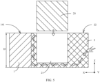
- the flow blocking part 21 is designed, in a process in which the second body 2 is formed by injection, flowing plastic is blocked by the mold 20 placed at a position of the flow blocking part 21, flows along a channel at a bottom end of the mold 20 to the first body 1, and contacts the first body 1, to generate a pressure in the first direction X on the first body 1. After a large amount of plastic is injected, the plastic is squeezed between the first body 1 and the flow blocking part 21 and flows in a third direction Z, to finally form the second body 2 that includes the flow blocking part 21.
- a pressure of the part of the plastic on the first body 1 in the first direction X is reduced when the plastic is injected, to ensure that, after sealing is performed on the sealing surface 11 of the first body 1, the plastic does not continuously flow in the first direction X, preventing plastic spreading along the sealing surface 11 of the first body 1 due to overflowing of plastic at a position at which the first body 1 and the second body 2 are bound in a processing process.
- This ensures sealing reliability of the sealing surface 11, improves sealing effect of the first body 1, increases a qualified rate of the frame 10, enables the first body 1 and the second body 2 to be well bound, and ensures smooth manufacturing of the frame 10.
- the pressure, on the first body 1 in the first direction X, of the plastic forming the second body 2 can be reduced, to still ensure the sealing reliability of the sealing surface 11 of the first body 1 when the first body 1 is thin, and meet a design requirement for the ultra-thin frame 10.
- the first direction X may be a width direction of the frame 10
- the second direction Y may be a length direction of the frame 10.
- the first direction X may alternatively be the length direction of the frame 10
- the second direction Y is the width direction of the frame 10.
- a pressure of injected plastic in a processing process can be reduced by using the frame 10, and when a screw hole is sealed at a position of an elastic piece in a liquid crystal display (Liquid Crystal Display, LCD) compartment, plastic blocking the screw hole and disqualification caused by plastic spreading during injection can be prevented.
- LCD liquid crystal Display
- the solution may also be applied to the following situation:
- a processing hole at the frame 10 has a large shut-off angle (for example, designed with a shut-off angle greater than 45°) and a large drop (for example, a drop is increased from 0.2 mm to 0.4 mm)
- the processing hole is prevented from being blocked by the plastic because the plastic spreads during injection, and a processing hole of an infrared alarm system at the frame is prevented from being blocked. This is not limited herein.
- the flow blocking part 21 extends to two sides of the sealing surface 11.
- a flow blocking range of the flow blocking part 21 can be increased, flow blocking effect of the flow blocking part 21 can be improved, and a channel at a bottom end of the mold 20 can be further extended, to prevent unsmooth plastic flowing because injected plastic is blocked at the bottom end of the mold 20 when the second body 2 is formed, improving injection efficiency of plastic.
- the pressure of the plastic flowing from the bottom end of the mold 20 to the first body 1 can be further reduced, to enable a pressure of the injected plastic to be distributed on two sides of the sealing surface 11 in the second direction Y, and to further reduce the pressure of the plastic on the first body 1 in the first direction X during injection. This enables the sealing surface 11 to block the injected plastic more easily and prevents the injected plastic from flowing along the sealing surface 11 under an action of the pressure, ensuring sealing reliability of the sealing surface 11 of the first body 1 and improving sealing effect.
- a shape of a cross-section of the flow blocking part 21 is one of a trapezoid, a rectangle, an ellipse, a triangle, and a pentagon.
- the cross-section of the flow blocking part 21 may be set to one of the trapezoid, the rectangle, the ellipse, the triangle, or the pentagon based on an arrangement requirement for an electronic component of the electronic device, to prevent interference between the frame 10 and the electronic component and improve installation stability of the electronic component while ensuring flow blocking effect of the flow blocking part 21. Further, installation space for the frame 10 can be properly allocated, space occupied by the electronic component can be reduced, system integration of the electronic device can be improved, and a lighter and thinner design requirement for the electronic device can be met.
- the cross-section of the flow blocking part 21 is a surface formed by cutting the flow blocking part 21 in the first direction X.
- the flow blocking part 21 is an approximately trapezoidal structure and is distributed on two sides of the sealing surface 11 in a second direction Y, to be adapted to installation of the electronic component of the electronic device in this embodiment.
- the flow blocking part 21 may alternatively be of another shape or a combination of a plurality of shapes, to be further accommodated to an installation requirement for the electronic component. This is not limited herein.
- a sunken part 12 configured to accommodate an electronic component is formed on the first body 1, and a protrusion 14 adjacent to the sunken part 12 is further formed on the first part 1, and the sealing surface 11 is formed on one side, adjacent to the sunken part 12, of the protrusion 14.
- the protrusion 14 and the sunken part 12 are provided to enable the frame 10 to be better attached to the electronic component and limit movement or displacement of the electronic component. This can improve installation stability of the electronic component, reduce occupation space for the electronic component, and improve system integration of the electronic device, to meet a lighter and thinner design requirement for the electronic device.
- plastic of the second body 2 is formed by injection, injected plastic generates a large positive pressure on the first body 1.
- the sunken part 12 is provided to enable the injected plastic to spread along one side, adjacent to the sunken part 12, of the protrusion 14 more easily.
- the sealing surface 11 is disposed on the side, adjacent to the sunken part 12, of the protrusion 14, to increase a pressure on the side, adjacent to the sunken part 12, of the protrusion 14 for blocking the injected plastic. This prevents the injected plastic from flowing along the sealing surface 11 under an action of the pressure, improves sealing effect of the first body 1, increases a qualified rate of the frame 10, and enables the first body 1 and the second body 2 to be bound well.
- an installation hole 13 is formed in the sunken part 12.
- the installation hole 13 is formed in the sunken part 12 to firmly connect an electronic component installed in the sunken part 12 to the frame 10 by using a fastener such as a screw, to further increase an attachment degree and a connection strength between the electronic component and the sunken part 12, limit relative displacement of the electronic component on the frame 10, prevent damage caused by shaking or vibration of the electronic component relative to the frame 10 during use of the electronic device, and improve structural stability of the electronic device.
- the first body 1 is relatively thin at a position of the sunken part 12, to facilitate processing of the installation hole 13 and improve processing efficiency of the frame.
- the installation hole 13 may alternatively be connected to the electronic component by embedding, snap-in, or the like. This is not limited herein.
- the installation hole 13 is provided at one end, away from the second body 2 in the first direction X, of the sunken part 12 of the first body 1. This can enable the installation hole 13 to be away from a position at which the first body 1 and the second body 2 are bound, to prevent injected plastic from flowing into the installation hole 13, causing the installation hole 13 to be blocked. Therefore, a qualified rate of the frame 10 is increased.
- a width of the sealing surface 11 is W, 0.5 mm ⁇ W ⁇ 10 mm, and a length of the sealing surface 11 is L, and 0.5 mm ⁇ L ⁇ 50 mm.
- W is 0.8 mm, 1 mm, 1.5 mm, 3 mm, or the like
- L is 0.8 mm, 3 mm, 10 mm, 20 mm, or the like.
- a specific size of the sealing surface 11 may be set based on a specific structure of the frame 10. This is not limited herein.
- the width W and the length L of the sealing surface 11 should not be excessively large or excessively small. If the width W of the sealing surface 11 is excessively large, namely, W>10 mm, space occupied by the sealing surface 11 in the third direction Z is easily excessively large. This enables the first body 1 to be excessively thick at the protrusion 14, which is not conducive to a light and thin design for the frame 10. Alternatively, this enables the first body 1 to be excessively thin at a position of the sunken part 12, which is not conducive to a strength design for the frame 10. If the width W of the sealing surface 11 is excessively small, namely, W ⁇ 0.5 mm, space occupied by the sealing surface 11 in the third direction Z is easily excessively small.
- the length direction of the sealing surface 11 is the same as an injection direction of the plastic forming the second body 2. This can increase the capability of the sealing surface 11 for resisting a pressure of the injected plastic and further improve the sealing effect of the first body 1.
- the length direction of the sealing surface 11 is the first direction X.
- the injection direction of the plastic forming the second body 2 is a different direction, it is only ensured that the length direction of the sealing surface 11 is the same as the injection direction of the plastic forming the second body 2. This is not limited herein.
- a size of the sealing surface 11 may be designed based on a specific size of the frame of the electronic device. For example, when the solution is applied to frame processing of a small electronic device, a width W of the small electronic device may be less than 0.5 mm, a length L may be less than 0.5 mm, or the like. When the solution is applied to frame processing of a large electronic device, a width W of the large electronic device may be greater than 10 mm, and a length L may be greater than 50 mm. This is not limited herein.
- a bottom surface of the sunken part 12 is higher than a bottom surface of the flow blocking part 21 in a third direction Z, and the third direction Z is a thickness direction of the frame 10.
- the flow blocking part 21 is designed, flowing plastic is blocked by the mold 20, flows along a channel at the bottom end of the mold 20 to the first body 1, and contacts the first body 1, to generate a pressure in the first direction X on the first body 1.
- the first body 1 bears a relatively great pressure, that is on a side wall on a side toward the second body 2, that is at a position lower than a bottom wall of the flow blocking part 21, and that is of injected plastic in the first direction X. Therefore, in the third direction Z, the bottom surface of the sunken part 12 is higher than the bottom surface of the flow blocking part 21. This can increase an area, in a direction toward the second body 2, of the first body 1 and increase a capability of the first body 1 for resisting a pressure of the injected plastic, effectively preventing plastic from overflowing during injection and improving sealing effect of the first body 1.
- a width of the gap is N, and 0.2 mm ⁇ N ⁇ 0.8 mm.
- N is 0.3 mm, 0.4 mm, 0.5 mm, 0.6 mm, 0.7 mm, or the like. This is not limited herein.
- the gap between the flow blocking part 21 and the first body 1 should not be excessively large or excessively small. If the width N of the gap is excessively large, that is, N>0.8 mm, excessively much plastic is pressed between the flow blocking part 21 and the first body 1 in the third direction Z, and a large pressure is still generated on the first body 1 in the first direction X. This easily causes injected plastic to flow along the surface of the first body 1, causing overflowing and reducing the qualified rate of the frame 10. If the width N of the gap is excessively small, that is, N ⁇ 0.2 mm, space between the first body 1 and the flow blocking part 21 is excessively small.
- the width N of the gap meets 0.2 mm ⁇ N ⁇ 0.8 mm, the width N of the gap between the flow blocking part 21 and the first body 1 is proper. Therefore, in a process in which the second body 2 is formed by processing, it can be ensured that the injected plastic can smoothly enter between the first body 1 and the flow blocking part 21. It is ensured that, when the second body 2 can be smoothly manufactured, there is not an excessively large amount of plastic flowing between the first body 1 and the flow blocking part 21. This prevents plastic overflowing because an excessively large pressure is generated, on the first body 1 in the first direction X, by the plastic before flowing between the first body 1 and the flow blocking part 21, improving sealing effect of the first body 1.
- a thickness of the first body 1 is D, and 0 mm ⁇ D ⁇ 0.8 mm.
- D may be 0.35 mm, 0.4 mm, 0.5 mm, 0.55 mm, 0.6 mm, 0.65 mm, 0.7 mm, or the like. This is not limited herein.
- an overall thickness of the frame 10 may be smaller, to meet a lighter and thinner design requirement for the frame 10. This enables the electronic device to be lighter and thinner, improving use experience of a user.
- the thickness D of the first body 1 may alternatively be designed as another value based on a specific design for the electronic device. This is not limited herein.
- a highest surface of the first body 1 is a first surface 141
- a highest surface of the second body 2 is a second surface 22.
- the first surface 141 and the second surface 22 are on a same plane.
- the first surface 141 and the second surface 22 are on the same plane, to ensure consistency of a position at which the first body 1 and the second body 2 are bound.
- This ensures flatness of an installation surface of the frame 10, increases integrity of the frame 10, and increases a connection strength between the first body 1 and the second body 2, to prevent damage, caused under a force in the first direction X, to the position at which the first body 1 and the second body 2 are bound, causing separation of the first body 1 and the second body 2, and increase an overall strength of the frame 10.
- the first direction X is a width direction of the frame 10
- the second direction Y is a length direction of the frame 10.
- the first direction X and the second direction Y may alternatively be other directions of the electronic device. This is not limited herein.
- An embodiment of this application further provides an electronic device.
- the electronic device includes an electronic component and the frame 10 in any one of the foregoing embodiments.
- the electronic component is installed on the frame 10. Because the frame 10 has the foregoing technical effect, the electronic device including the frame 10 should also have corresponding technical effect. Details are not described herein again.
Landscapes
- Engineering & Computer Science (AREA)
- Signal Processing (AREA)
- Microelectronics & Electronic Packaging (AREA)
- Casings For Electric Apparatus (AREA)
Abstract
Description
- This application claims priority to
Chinese Patent Application No. 202211498086.6, filed with the China National Intellectual Property Administration on November 28, 2022 - This application relates to the technical field of electronic devices, and in particular to a frame and an electronic device.
- As electronic products are continuously updated, electronic devices are increasingly lighter and thinner. Structural members of the electronic devices also need to be lighter and thinner.
- The electronic device usually includes a frame jointly formed by alloy and plastic. During processing, sealing is to be performed on thin alloy at some specific positions. When sealing is performed on the thin alloy, sealing effect is poor because the alloy is excessively thin.
- This application provides a frame and an electronic device, to resolve a problem in the conventional technology that sealing effect is poor because alloy is excessively thin.
- According to a first aspect, an embodiment of this application provides a frame. The frame includes a first body and a second body. The first body includes a sealing surface, and the second body includes a flow blocking part sunken toward one side. An extension surface of the sealing surface intersects the flow blocking part in a first direction X.
- In this solution, because the flow blocking part is designed, in a process in which the second body is formed by injection, flowing plastic is blocked by a mold placed at a position of the flow blocking part, flows along a channel at a bottom end of the mold to the first body, and contacts the first body, to generate a pressure in the first direction X on the first body. After a large amount of plastic is injected, the plastic is squeezed between the first body and the flow blocking part and flows in a third direction, to finally form the second body that includes the flow blocking part. Because a part, formed between the first body and the flow blocking part, of the plastic flows in the third direction Z, a pressure of the part of the plastic on the first body in the first direction X is reduced when the plastic is injected, to ensure that, after sealing is performed on the sealing surface of the first body, the plastic does not continuously flow in the first direction, preventing plastic spreading along the sealing surface of the first body due to overflowing of plastic at a position at which the first body and the second body are bound in a processing process. This ensures sealing reliability of the sealing surface, improves sealing effect of the first body, increases a qualified rate of the frame, enables the first body and the second body to be bound well, and ensures smooth manufacturing of the frame. In addition, because the frame of this structure can reduce the pressure, on the first body in the first direction, of the plastic that forms the second body, the sealing reliability of the sealing surface of the first body can still be ensured when the first body is thin, to meet a design requirement for an ultra-thin frame.
- In a possible design, the flow blocking part extends to two sides of the sealing surface in a second direction.
- In this solution, in the structure design, a flow blocking range of the flow blocking part can be increased, flow blocking effect of the flow blocking part can be improved, and a channel at a bottom end of the mold can be further extended, to prevent unsmooth plastic flowing because injected plastic is blocked at the bottom end of the mold when the second body is formed, improving injection efficiency of plastic. In addition, the pressure of the plastic flowing from the bottom end of the mold to the first body can be further reduced, to enable a pressure of the injected plastic to be distributed on two sides of the sealing surface in the second direction, and to further reduce the pressure of the plastic on the first body in the first direction during injection. This enables the sealing surface to block the injected plastic more easily and prevents the injected plastic from flowing along the sealing surface under an action of the pressure, ensuring sealing reliability of the sealing surface of the first body and improving sealing effect.
- In a possible design, a sunken part configured to accommodate an electronic component is formed on the first body, a protrusion adjacent to the sunken part is further formed on the first body, and the sealing surface is formed on a side, adjacent to the sunken part, of the protrusion.
- In this solution, the protrusion and the sunken part are provided to enable the frame to be better attached to the electronic component and limit movement or displacement of the electronic component. This can improve installation stability of the electronic component, reduce occupation space for the electronic component, and improve system integration of the electronic device, to meet a lighter and thinner design requirement for the electronic device. The sealing surface is disposed on the side, adjacent to the sunken part, of the protrusion, to increase a pressure on the side, adjacent to the sunken part, of the protrusion for blocking the injected plastic. This prevents the injected plastic from flowing along the sealing surface under an action of the pressure, improves sealing effect of the first body, increases a qualified rate of the frame, and enables the first body and the second body to be bound well.
- In a possible design, an installation hole is formed in the sunken part.
- In this solution, the installation hole is formed in the sunken part, to firmly connect an electronic component installed in the sunken part to the frame by using a fastener such as a screw, to further increase an attachment degree and a connection strength between the electronic component and the sunken part, limit relative displacement of the electronic component on the frame, prevent damage caused by shaking or vibration of the electronic component relative to the frame during use of the electronic device, and improve structural stability of the electronic device. In addition, the first body is relatively thin at a position of the sunken part, to facilitate processing of the installation hole and improve processing efficiency of the frame.
- In a possible design, a width of the sealing surface is W, and 0.5 mm≤W≤10 mm, and a length of the sealing surface is L, and 0.5 mm≤L≤50 mm. For example, W is 0.8 mm, 1 mm, 1.5 mm, 3 mm, or the like, and L is 0.8 mm, 3 mm, 10 mm, 20 mm, or the like. A specific size of the sealing
surface 11 may be set based on a specific structure of theframe 10. This is not limited herein. - In this solution, when the width W of the sealing surface meets 0.5 mm≤W≤10 mm, and the length L meets 0.5 mm≤L≤50 mm, a size of the sealing surface is proper, and a thickness of the first body at the protrusion and the sunken part is proper. This can meet a light and thin design requirement for the frame, an overall strength design requirement for the frame, and an installation requirement for the frame for the electronic component, reduce a processing difficulty for the installation hole, enable a strength of the first body on the sealing surface to be increased, and enable a capability of resisting a pressure of the injected plastic to be increased. Therefore, when the second body is formed, the injected plastic can be prevented from spreading along the sealing surface, to improve sealing effect of the first body.
- In a possible design, a bottom surface of the sunken part is higher than a bottom surface of the flow blocking part in a third direction, and the third direction is a thickness direction of the frame.
- In this solution, because the flow blocking part is designed, flowing plastic is blocked by a mold, flows along a channel at a bottom end of the mold to the first body, and contacts the first body, to generate a pressure in the first direction on the first body. To be specific, the first body bears a relatively great pressure that is on a side wall on a side toward the second body, that is at a position lower than a bottom wall of the flow blocking part, and that is of injected plastic in the first direction. Therefore, in the third direction, the bottom surface of the sunken part is higher than the bottom surface of the flow blocking part. This can increase an area, in a direction toward the second body, of the first body and increase a capability of the first body for resisting a pressure of the injected plastic, effectively preventing plastic from overflowing during injection and improving sealing effect of the first body.
- In a possible design, in the first direction, there is a gap between the flow blocking part and the first body, a width of the gap is N, and 0.2 mm≤N≤0.8 mm. For example, N is 0.3 mm, 0.4 mm, 0.5 mm, 0.6 mm, 0.7 mm, or the like. This is not limited herein.
- In this solution, when the width N of the gap meets 0.2 mm≤N≤0.8 mm, the width N of the gap between the flow blocking part and the first body is proper. Therefore, in a process in which the second body is formed by processing, it can be ensured that the injected plastic can smoothly enter between the first body and the flow blocking part. It is ensured, when the second body can be smoothly manufactured, that there is not an excessively large amount of plastic flowing between the first body and the flow blocking part. This prevents plastic overflowing because an excessively large pressure is generated, on the first body in the first direction, by the plastic before flowing between the first body and the flow blocking part, improving sealing effect of the first body.
- In a possible design, a shape of a cross-section of the flow blocking part is one of a trapezoid, a rectangle, an ellipse, a triangle, and a pentagon.
- In this solution, the flow blocking part may be set to one of the trapezoid, the rectangle, the ellipse, the triangle, or the pentagon based on an arrangement requirement for an electronic component of the electronic device, to prevent interference between the frame and the electronic component and improve installation stability of the electronic component while ensuring flow blocking effect of the flow blocking part. Further, installation space for the frame can be properly allocated, space occupied by the electronic component can be reduced, system integration of the electronic device can be improved, and a lighter and thinner design requirement for the electronic device can be met.
- In a possible design, a thickness of the first body is D, and 0 mm<D≤0.8 mm. For example, D may be 0.35 mm, 0.4 mm, 0.5 mm, 0.55 mm, 0.6 mm, 0.65 mm, 0.7 mm, or the like. This is not limited herein.
- In this solution, when the thickness D of the first body is less than or equal to 0.8 mm, an overall thickness of the frame may be smaller, to meet a lighter and thinner design requirement for the frame. This enables the electronic device to be lighter and thinner, improving use experience of a user.
- In a possible design, in the third direction, a highest surface of the first body is a first surface, and a highest surface of the second body is a second surface. The first surface and the second surface are on a same plane.
- In this solution, the first surface and the second surface are on the same plane in the third direction, to ensure consistency of a position at which the first body and the second body are bound. This ensures flatness of an installation surface of the frame, increases integrity of the frame, and can increase a connection strength between the first body and the second body, to prevent damage, caused under a force in the first direction, to the position at which the first body and the second body are bound, causing separation of the first body and the second body, and increase an overall strength of the frame.
- In a possible design, the first direction is a width direction of the frame, and the second direction is a length direction of the frame. Certainly, based on different reference coordinates of the electronic device, the first direction and the second direction may alternatively be other directions of the electronic device. This is not limited herein.
- According to a second aspect, an embodiment of this application further provides an electronic device. The electronic device includes an electronic component and the frame described in any one of the foregoing embodiments. The electronic component is installed on the frame. Because the frame has the foregoing technical effect, the electronic device including the frame should also have corresponding technical effect. Details are not described herein again.
- It should be understood that the foregoing general description and the following detailed description are merely examples, and cannot limit this application.
-
-
FIG. 1 is a schematic diagram of a partial structure of a frame of an electronic device in the conventional technology; -
FIG. 2 is a principle diagram of a processing process of the frame inFIG. 1 ; -
FIG. 3 is a schematic diagram of a structure of a frame of an electronic device according to an embodiment of this application; -
FIG. 4 is a partially enlarged view of the frame at a position A inFIG. 3 ; -
FIG. 5 is a principle diagram of a processing process of the frame inFIG. 3 ; -
FIG. 6 is a schematic diagram of a partial structure of the frame inFIG. 1 at another angle; and -
FIG. 7 is a partially enlarged view at a position B inFIG. 4 . -
- 1'-first body;
- 2'-second body;
- 3'-mold;
- 10-frame;
- 1-first body;
- 11-sealing surface;
- 12-sunken part;
- 13-installation hole;
- 14-protrusion;
141-first surface;
- 2-second body;
- 21-flow blocking part;
- 22-second surface;
- 20-mold;
- X-first direction;
- Y-second direction;
- Z-third direction.
- The accompanying drawings herein are incorporated into the specification and constitute a part of the specification, show embodiments conforming to this application, and are used together with the specification to explain a principle of this application.
- Description of conventional technologies: In a conventional design solution for a frame of an electronic device, a limit value of sealing space for an alloy part of the frame is ensured to be 0.7 mm. For a processing hole formed on a frame with a thickness less than 0.8 mm, a shut-off difference is designed based on 45°, and a segment difference is ensured to be 0.35 mm or above. Sealing for shut-off is preferably performed in a single direction, followed by adjacent shut-off, and simultaneous shut-off in three directions is prohibited. In this design solution, a requirement for a wall thickness of the alloy part is relatively high, and the wall thickness of the alloy part is to be at least greater than 1 mm. When the wall thickness of the alloy part at a specific position is less than 1 mm, disqualification caused by plastic spreading may easily occur while sealing is performed in this method.
- As electronic products are continuously updated, electronic devices are increasingly lighter and thinner. Structural members of the electronic devices also need to be lighter and thinner.
FIG. 1 is a schematic diagram of a structure of a frame of an existing electronic device. The frame includes and is jointly formed by afirst body 1' of an alloy material and a second body 2' of a plastic material. The second body 2' is formed at thefirst body 1' by injection. As shown inFIG. 2 , during processing, because thefirst body 1' is excessively light and thin (for example, when a thickness of thefirst body 1' is less than 0.8 mm), a sealing width of thefirst body 1' is not large enough and cannot meet a sealing requirement for a position at which thefirst body 1' and the second body 2' are bound, and a pressure resistance capability is low. This causes plastic that forms the second body 2' to generate a large pressure in a direction toward thefirst body 1' in an injection process, and causes a part of the plastic to easily flow in a gap between a mold 3' and thefirst body 1' along an inner wall of thefirst body 1', resulting in disqualification caused by plastic spreading and affecting a qualified rate of the frame. - To resolve the foregoing technical problem, embodiments of this application provide a frame and an electronic device, to ensure, when an alloy part of the frame is relatively thin, sealing effect at a position at which the alloy part and a plastic part are bound. The electronic device in embodiments of this application includes, for example, a mobile phone, a tablet computer, an ultra-mobile personal computer (ultra-mobile personal computer, UMPC), a netbook, a cellular phone, a personal digital assistant (personal digital assistant, PDA), an augmented reality (augmented reality, AR) device, a virtual reality (virtual reality, VR) device, an artificial intelligence (artificial intelligence, AI) device, a wearable device, an in-vehicle device, a smart home device and/or a smart city device, a game handle, and any terminal electronic device that may have a frame configured to install an electronic component. A specific form of the electronic device is not specially limited in embodiments of this application. For ease of description, for example, the electronic device is a mobile phone for description.
- To better understand technical solutions of this application, the following describes embodiments of this application in detail with reference to accompanying drawings.
- An embodiment of this application provides a
frame 10. As shown inFIG. 3 andFIG. 4 , theframe 10 includes afirst body 1 and asecond body 2. Thefirst body 1 includes a sealingsurface 11, and thesecond body 2 includes aflow blocking part 21 sunken toward one side. An extension surface of the sealingsurface 11 intersects theflow blocking part 21 in a first direction X. Thefirst body 1 may be made of an alloy material, and thesecond body 2 may be made of a plastic material. Thefirst body 1 and thesecond body 2 may alternatively be made of other materials that form theframe 10 by sealing. - As shown in
FIG. 3 to FIG. 5 , in a specific implementation, theframe 10 includes and is jointly formed by thefirst body 1 of the alloy material and thesecond body 2 of the plastic material, and thesecond body 2 is formed at thefirst body 1 by injection. During processing, sealing is performed on the sealingsurface 11 by using a sealing mold, and fastening is performed by using amold 20 at a position at which thesecond body 2 is formed. Then, plastic is injected to form thesecond body 2 that includes theflow blocking part 21, and the sealing mold and themold 20 are removed to form theframe 10. - In this embodiment, as shown in an arrow direction in
FIG. 5 , because theflow blocking part 21 is designed, in a process in which thesecond body 2 is formed by injection, flowing plastic is blocked by themold 20 placed at a position of theflow blocking part 21, flows along a channel at a bottom end of themold 20 to thefirst body 1, and contacts thefirst body 1, to generate a pressure in the first direction X on thefirst body 1. After a large amount of plastic is injected, the plastic is squeezed between thefirst body 1 and theflow blocking part 21 and flows in a third direction Z, to finally form thesecond body 2 that includes theflow blocking part 21. Because a part, formed between thefirst body 1 and theflow blocking part 21, of the plastic flows in the third direction Z, a pressure of the part of the plastic on thefirst body 1 in the first direction X is reduced when the plastic is injected, to ensure that, after sealing is performed on the sealingsurface 11 of thefirst body 1, the plastic does not continuously flow in the first direction X, preventing plastic spreading along the sealingsurface 11 of thefirst body 1 due to overflowing of plastic at a position at which thefirst body 1 and thesecond body 2 are bound in a processing process. This ensures sealing reliability of the sealingsurface 11, improves sealing effect of thefirst body 1, increases a qualified rate of theframe 10, enables thefirst body 1 and thesecond body 2 to be well bound, and ensures smooth manufacturing of theframe 10. In addition, in a manufacturing process of theframe 10 of the structure, the pressure, on thefirst body 1 in the first direction X, of the plastic forming thesecond body 2 can be reduced, to still ensure the sealing reliability of the sealingsurface 11 of thefirst body 1 when thefirst body 1 is thin, and meet a design requirement for theultra-thin frame 10. - In this embodiment of this application, two of the first direction X, the second direction Y, and the third direction Z are roughly perpendicular to each other. The first direction X may be a width direction of the
frame 10, and the second direction Y may be a length direction of theframe 10. Certainly, the first direction X may alternatively be the length direction of theframe 10, and correspondingly, the second direction Y is the width direction of theframe 10. - In this embodiment of this application, a pressure of injected plastic in a processing process can be reduced by using the
frame 10, and when a screw hole is sealed at a position of an elastic piece in a liquid crystal display (Liquid Crystal Display, LCD) compartment, plastic blocking the screw hole and disqualification caused by plastic spreading during injection can be prevented. Further, the solution may also be applied to the following situation: When a processing hole at theframe 10 has a large shut-off angle (for example, designed with a shut-off angle greater than 45°) and a large drop (for example, a drop is increased from 0.2 mm to 0.4 mm), the processing hole is prevented from being blocked by the plastic because the plastic spreads during injection, and a processing hole of an infrared alarm system at the frame is prevented from being blocked. This is not limited herein. - In a specific embodiment, as shown in
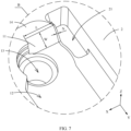
FIG. 6 andFIG. 7 , in the second direction Y, theflow blocking part 21 extends to two sides of the sealingsurface 11. - In this embodiment, as shown in
FIG. 5 to FIG. 7 , in the structure design, a flow blocking range of theflow blocking part 21 can be increased, flow blocking effect of theflow blocking part 21 can be improved, and a channel at a bottom end of themold 20 can be further extended, to prevent unsmooth plastic flowing because injected plastic is blocked at the bottom end of themold 20 when thesecond body 2 is formed, improving injection efficiency of plastic. In addition, the pressure of the plastic flowing from the bottom end of themold 20 to thefirst body 1 can be further reduced, to enable a pressure of the injected plastic to be distributed on two sides of the sealingsurface 11 in the second direction Y, and to further reduce the pressure of the plastic on thefirst body 1 in the first direction X during injection. This enables the sealingsurface 11 to block the injected plastic more easily and prevents the injected plastic from flowing along the sealingsurface 11 under an action of the pressure, ensuring sealing reliability of the sealingsurface 11 of thefirst body 1 and improving sealing effect. - In a specific embodiment, as shown in
FIG. 6 andFIG. 7 , a shape of a cross-section of theflow blocking part 21 is one of a trapezoid, a rectangle, an ellipse, a triangle, and a pentagon. - In this embodiment, as shown in
FIG. 6 andFIG. 7 , the cross-section of theflow blocking part 21 may be set to one of the trapezoid, the rectangle, the ellipse, the triangle, or the pentagon based on an arrangement requirement for an electronic component of the electronic device, to prevent interference between theframe 10 and the electronic component and improve installation stability of the electronic component while ensuring flow blocking effect of theflow blocking part 21. Further, installation space for theframe 10 can be properly allocated, space occupied by the electronic component can be reduced, system integration of the electronic device can be improved, and a lighter and thinner design requirement for the electronic device can be met. - In this embodiment, the cross-section of the
flow blocking part 21 is a surface formed by cutting theflow blocking part 21 in the first direction X. - In the specific embodiment shown in
FIG. 6 andFIG. 7 , theflow blocking part 21 is an approximately trapezoidal structure and is distributed on two sides of the sealingsurface 11 in a second direction Y, to be adapted to installation of the electronic component of the electronic device in this embodiment. - Certainly, the
flow blocking part 21 may alternatively be of another shape or a combination of a plurality of shapes, to be further accommodated to an installation requirement for the electronic component. This is not limited herein. - In a specific embodiment, as shown in
FIG. 4 ,FIG. 6 , andFIG. 7 , asunken part 12 configured to accommodate an electronic component is formed on thefirst body 1, and aprotrusion 14 adjacent to thesunken part 12 is further formed on thefirst part 1, and the sealingsurface 11 is formed on one side, adjacent to thesunken part 12, of theprotrusion 14. - In this embodiment, as shown in
FIG. 4 ,FIG. 6 , andFIG. 7 , theprotrusion 14 and thesunken part 12 are provided to enable theframe 10 to be better attached to the electronic component and limit movement or displacement of the electronic component. This can improve installation stability of the electronic component, reduce occupation space for the electronic component, and improve system integration of the electronic device, to meet a lighter and thinner design requirement for the electronic device. When plastic of thesecond body 2 is formed by injection, injected plastic generates a large positive pressure on thefirst body 1. Thesunken part 12 is provided to enable the injected plastic to spread along one side, adjacent to thesunken part 12, of theprotrusion 14 more easily. Therefore, the sealingsurface 11 is disposed on the side, adjacent to thesunken part 12, of theprotrusion 14, to increase a pressure on the side, adjacent to thesunken part 12, of theprotrusion 14 for blocking the injected plastic. This prevents the injected plastic from flowing along the sealingsurface 11 under an action of the pressure, improves sealing effect of thefirst body 1, increases a qualified rate of theframe 10, and enables thefirst body 1 and thesecond body 2 to be bound well. - In a specific embodiment, as shown in
FIG. 4 ,FIG. 6 , andFIG. 7 , aninstallation hole 13 is formed in thesunken part 12. - In this embodiment, as shown in
FIG. 4 ,FIG. 6 , andFIG. 7 , theinstallation hole 13 is formed in thesunken part 12 to firmly connect an electronic component installed in thesunken part 12 to theframe 10 by using a fastener such as a screw, to further increase an attachment degree and a connection strength between the electronic component and thesunken part 12, limit relative displacement of the electronic component on theframe 10, prevent damage caused by shaking or vibration of the electronic component relative to theframe 10 during use of the electronic device, and improve structural stability of the electronic device. In addition, thefirst body 1 is relatively thin at a position of thesunken part 12, to facilitate processing of theinstallation hole 13 and improve processing efficiency of the frame. - The
installation hole 13 may alternatively be connected to the electronic component by embedding, snap-in, or the like. This is not limited herein. - In addition, as shown in
FIG. 6 andFIG. 7 , theinstallation hole 13 is provided at one end, away from thesecond body 2 in the first direction X, of thesunken part 12 of thefirst body 1. This can enable theinstallation hole 13 to be away from a position at which thefirst body 1 and thesecond body 2 are bound, to prevent injected plastic from flowing into theinstallation hole 13, causing theinstallation hole 13 to be blocked. Therefore, a qualified rate of theframe 10 is increased. - In a specific embodiment, as shown in
FIG. 7 , a width of the sealingsurface 11 is W, 0.5 mm≤W≤10 mm, and a length of the sealingsurface 11 is L, and 0.5 mm≤L≤50 mm. For example, W is 0.8 mm, 1 mm, 1.5 mm, 3 mm, or the like, and L is 0.8 mm, 3 mm, 10 mm, 20 mm, or the like. A specific size of the sealingsurface 11 may be set based on a specific structure of theframe 10. This is not limited herein. - As shown in
FIG. 7 , the width W and the length L of the sealingsurface 11 should not be excessively large or excessively small. If the width W of the sealingsurface 11 is excessively large, namely, W>10 mm, space occupied by the sealingsurface 11 in the third direction Z is easily excessively large. This enables thefirst body 1 to be excessively thick at theprotrusion 14, which is not conducive to a light and thin design for theframe 10. Alternatively, this enables thefirst body 1 to be excessively thin at a position of thesunken part 12, which is not conducive to a strength design for theframe 10. If the width W of the sealingsurface 11 is excessively small, namely, W<0.5 mm, space occupied by the sealingsurface 11 in the third direction Z is easily excessively small. This enables thesunken part 12 to be not deep enough, is not conducive to limitation of the electronic component and a light and thin design for the electronic device, and increases a processing difficulty for theinstallation hole 13. If the length L of the sealingsurface 11 is excessively large, namely, L>50 mm, space occupied by the sealingsurface 11 in a length direction of the sealingsurface 11 is easily excessively large, and a size of theframe 10 is increased, which is not conducive to a miniaturization design for the electronic device. If the length L of the sealingsurface 11 is excessively small, that is, L<0.5 mm, space occupied by the sealingsurface 11 in a length direction of the sealingsurface 11 is excessively small. This enables a sealing strength of a sealing mold on the sealingsurface 11 to be reduced and a capability of resisting a pressure of injected plastic to be reduced, causing disqualification caused by plastic spreading because the injected plastic easily flows along the sealingsurface 11, when thesecond body 2 is formed. - In this embodiment, as shown in
FIG. 7 , when the width W of the sealingsurface 11 meets 0.5 mm≤W≤10 mm, and the length L meets 0.5 mm≤L≤50 mm, a size of the sealingsurface 11 is proper, and a thickness of thefirst body 1 at theprotrusion 14 and thesunken part 12 is proper. This can meet a light and thin design requirement for theframe 10, an overall strength design requirement for theframe 10, and an installation requirement for theframe 10 for the electronic component, reduce a processing difficulty for theinstallation hole 13, enable a strength of thefirst body 1 on the sealingsurface 11 to be increased, and enable a capability of resisting a pressure of the injected plastic to be increased. Therefore, when thesecond body 2 is formed, the injected plastic can be prevented from spreading along the sealingsurface 11, to improve sealing effect of thefirst body 1. - The length direction of the sealing
surface 11 is the same as an injection direction of the plastic forming thesecond body 2. This can increase the capability of the sealingsurface 11 for resisting a pressure of the injected plastic and further improve the sealing effect of thefirst body 1. In the specific embodiment shown inFIG. 7 , the length direction of the sealingsurface 11 is the first direction X. Certainly, when the injection direction of the plastic forming thesecond body 2 is a different direction, it is only ensured that the length direction of the sealingsurface 11 is the same as the injection direction of the plastic forming thesecond body 2. This is not limited herein. - Certainly, when the solution in this embodiment is applied to another small electronic device or another large electronic device, a size of the sealing
surface 11 may be designed based on a specific size of the frame of the electronic device. For example, when the solution is applied to frame processing of a small electronic device, a width W of the small electronic device may be less than 0.5 mm, a length L may be less than 0.5 mm, or the like. When the solution is applied to frame processing of a large electronic device, a width W of the large electronic device may be greater than 10 mm, and a length L may be greater than 50 mm. This is not limited herein. - In a specific embodiment, as shown in
FIG. 4 ,FIG. 6 , andFIG. 7 , a bottom surface of thesunken part 12 is higher than a bottom surface of theflow blocking part 21 in a third direction Z, and the third direction Z is a thickness direction of theframe 10. - In this embodiment, as shown in an arrow direction in
FIG. 5 , because theflow blocking part 21 is designed, flowing plastic is blocked by themold 20, flows along a channel at the bottom end of themold 20 to thefirst body 1, and contacts thefirst body 1, to generate a pressure in the first direction X on thefirst body 1. To be specific, thefirst body 1 bears a relatively great pressure, that is on a side wall on a side toward thesecond body 2, that is at a position lower than a bottom wall of theflow blocking part 21, and that is of injected plastic in the first direction X. Therefore, in the third direction Z, the bottom surface of thesunken part 12 is higher than the bottom surface of theflow blocking part 21. This can increase an area, in a direction toward thesecond body 2, of thefirst body 1 and increase a capability of thefirst body 1 for resisting a pressure of the injected plastic, effectively preventing plastic from overflowing during injection and improving sealing effect of thefirst body 1. - In a specific embodiment, as shown in
FIG. 4 to FIG. 7 , in the first direction X, there is a gap between theflow blocking part 21 and thefirst body 1, a width of the gap is N, and 0.2 mm≤N≤0.8 mm. For example, N is 0.3 mm, 0.4 mm, 0.5 mm, 0.6 mm, 0.7 mm, or the like. This is not limited herein. - In this embodiment, as shown in
FIG. 4 to FIG. 7 , the gap between theflow blocking part 21 and thefirst body 1 should not be excessively large or excessively small. If the width N of the gap is excessively large, that is, N>0.8 mm, excessively much plastic is pressed between theflow blocking part 21 and thefirst body 1 in the third direction Z, and a large pressure is still generated on thefirst body 1 in the first direction X. This easily causes injected plastic to flow along the surface of thefirst body 1, causing overflowing and reducing the qualified rate of theframe 10. If the width N of the gap is excessively small, that is, N<0.2 mm, space between thefirst body 1 and theflow blocking part 21 is excessively small. Therefore, in a process in which thesecond body 2 is formed by processing, injected plastic is not easily pressed between thefirst body 1 and theflow blocking part 21, causing plastic to accumulate at a bottom of theflow blocking part 21. This is not conducive to processing and forming of thesecond body 2 and reduces a processing yield of theframe 10. - Therefore, when the width N of the gap meets 0.2 mm≤N≤0.8 mm, the width N of the gap between the
flow blocking part 21 and thefirst body 1 is proper. Therefore, in a process in which thesecond body 2 is formed by processing, it can be ensured that the injected plastic can smoothly enter between thefirst body 1 and theflow blocking part 21. It is ensured that, when thesecond body 2 can be smoothly manufactured, there is not an excessively large amount of plastic flowing between thefirst body 1 and theflow blocking part 21. This prevents plastic overflowing because an excessively large pressure is generated, on thefirst body 1 in the first direction X, by the plastic before flowing between thefirst body 1 and theflow blocking part 21, improving sealing effect of thefirst body 1. - In a specific embodiment, as shown in
FIG. 4 andFIG. 5 , a thickness of thefirst body 1 is D, and 0 mm<D≤0.8 mm. For example, D may be 0.35 mm, 0.4 mm, 0.5 mm, 0.55 mm, 0.6 mm, 0.65 mm, 0.7 mm, or the like. This is not limited herein. - In this embodiment, as shown in
FIG. 4 andFIG. 5 , when the thickness D of thefirst body 1 is less than or equal to 0.8 mm, an overall thickness of theframe 10 may be smaller, to meet a lighter and thinner design requirement for theframe 10. This enables the electronic device to be lighter and thinner, improving use experience of a user. - Certainly, the thickness D of the
first body 1 may alternatively be designed as another value based on a specific design for the electronic device. This is not limited herein. - In a specific embodiment, as shown in
FIG. 4 to FIG. 7 , in the third direction Z, a highest surface of thefirst body 1 is afirst surface 141, and a highest surface of thesecond body 2 is asecond surface 22. Thefirst surface 141 and thesecond surface 22 are on a same plane. - In this embodiment, as shown in
FIG. 4 to FIG. 7 , in the third direction Z, thefirst surface 141 and thesecond surface 22 are on the same plane, to ensure consistency of a position at which thefirst body 1 and thesecond body 2 are bound. This ensures flatness of an installation surface of theframe 10, increases integrity of theframe 10, and increases a connection strength between thefirst body 1 and thesecond body 2, to prevent damage, caused under a force in the first direction X, to the position at which thefirst body 1 and thesecond body 2 are bound, causing separation of thefirst body 1 and thesecond body 2, and increase an overall strength of theframe 10. - In a specific embodiment, as shown in
FIG. 4 to FIG. 7 , the first direction X is a width direction of theframe 10, and the second direction Y is a length direction of theframe 10. Certainly, based on different reference coordinates of the electronic device, the first direction X and the second direction Y may alternatively be other directions of the electronic device. This is not limited herein. - An embodiment of this application further provides an electronic device. The electronic device includes an electronic component and the
frame 10 in any one of the foregoing embodiments. The electronic component is installed on theframe 10. Because theframe 10 has the foregoing technical effect, the electronic device including theframe 10 should also have corresponding technical effect. Details are not described herein again. - It should be noted that a part of the application document of this patent includes copyright-protected content. A copyright owner reserves the copyright except copies made for the patent document or the recorded content of the patent document in the China National Intellectual Property Administration.
Claims (19)
- A frame, comprising:a first body (1), comprising a sealing surface (11); anda second body (2), comprising a flow blocking part (21) sunken toward one side, whereinan extension surface of the sealing surface (11) intersects the flow blocking part (21) in a first direction (X).
- The frame according to claim 1, wherein the flow blocking part (21) extends to two sides of the sealing surface (11) in a second direction (Y).
- The frame according to claim 1, wherein a sunken part (12) configured to accommodate an electronic component is formed on the first body (1); and
a protrusion (14) adjacent to the sunken part (12) is further formed on the first body (1); and the sealing surface (11) is formed on a side, adjacent to the sunken part (12), of the protrusion (14). - The frame according to claim 3, wherein an installation hole (13) is formed in the sunken part (12).
- The frame according to claim 4, wherein a width of the sealing surface (11) is W, and 0.5 mm≤W≤10 mm; and
a length of the sealing surface (11) is L, and 0.5 mm≤L≤50 mm. - The frame according to claim 4, wherein a bottom surface of the sunken part (12) is higher than a bottom surface of the flow blocking part (21) in a third direction (Z); and the third direction (Z) is a thickness direction of the frame (10).
- The frame according to any one of claims 1 to 6, wherein there is a gap between the flow blocking part (21) and the first body (1) in the first direction (X); and
a width of the gap is N, and 0.2 mm≤N≤0.8 mm. - The frame according to any one of claims 1 to 6, wherein a shape of a cross-section of the flow blocking part (21) is one of a trapezoid, a rectangle, an ellipse, a triangle, and a pentagon.
- The frame according to any one of claims 1 to 6, wherein a thickness of the first body (1) is D, and 0 mm<D≤0.8 mm.
- The frame according to any one of claims 1 to 6, wherein in the third direction (Z), a highest surface of the first body (1) is a first surface (141), and a highest surface of the second body (2) is a second surface (22); and
the first surface (141) and the second surface (22) are on a same plane. - The frame according to claim 2, wherein the first direction (X) is a width direction of the frame (10), and the second direction (Y) is a length direction of the frame (10).
- An electronic device, wherein the electronic device comprises an electronic component and the frame (10) according to any one of claims 1 to 11, and the electronic component is installed on the frame (10).
- A frame, comprising:a first body (1), comprising a sealing surface (11); anda second body (2), comprising a flow blocking part (21) sunken toward one side, whereinan extension surface of the sealing surface (11) intersects the flow blocking part (21) in a first direction (X);the flow blocking part (21) extends to two sides of the sealing surface (11) in a second direction (Y);a sunken part (12) configured to accommodate an electronic component is formed on the first body (1), and an installation hole (13) is formed in the sunken part (12);there is a gap between the flow blocking part (21) and the first body (1) in the first direction (X), wherein a width of the gap is N, and 0.2 mm≤N≤0.8 mm; anda thickness of the first body (1) is D, and 0 mm<D≤0.8 mm.
- The frame according to claim 13, wherein a protrusion (14) adjacent to the sunken part (12) is further formed on the first body (1); and the sealing surface (11) is formed on a side, adjacent to the sunken part (12), of the protrusion (14).
- The frame according to claim 13, wherein a width of the sealing surface (11) is W, and 0.5 mm≤W≤10 mm; and
a length of the sealing surface (11) is L, and 0.5 mm≤L≤50 mm. - The frame according to claim 13, wherein a bottom surface of the sunken part (12) is higher than a bottom surface of the flow blocking part (21) in a third direction (Z); and the third direction (Z) is a thickness direction of the frame (10).
- The frame according to any one of claims 13 to 16, wherein a shape of a cross-section of the flow blocking part (21) is one of a trapezoid, a rectangle, an ellipse, a triangle, and a pentagon.
- The frame according to any one of claims 13 to 16, wherein in the third direction (Z), a highest surface of the first body (1) is a first surface (141), and a highest surface of the second body (2) is a second surface (22); and
the first surface (141) and the second surface (22) are on a same plane. - The frame according to claim 13, wherein the first direction (X) is a width direction of the frame (10), and the second direction (Y) is a length direction of the frame (10).
Applications Claiming Priority (2)
| Application Number | Priority Date | Filing Date | Title |
|---|---|---|---|
| CN202211498086.6A CN115604385B (en) | 2022-11-28 | 2022-11-28 | Frame and electronic equipment |
| PCT/CN2023/116112 WO2024114002A1 (en) | 2022-11-28 | 2023-08-31 | Frame, and electronic device |
Publications (3)
| Publication Number | Publication Date |
|---|---|
| EP4401391A1 true EP4401391A1 (en) | 2024-07-17 |
| EP4401391A4 EP4401391A4 (en) | 2024-12-04 |
| EP4401391B1 EP4401391B1 (en) | 2025-10-08 |
Family
ID=84852108
Family Applications (1)
| Application Number | Title | Priority Date | Filing Date |
|---|---|---|---|
| EP23829498.7A Active EP4401391B1 (en) | 2022-11-28 | 2023-08-31 | Frame, and electronic device |
Country Status (4)
| Country | Link |
|---|---|
| US (1) | US12543283B2 (en) |
| EP (1) | EP4401391B1 (en) |
| CN (1) | CN115604385B (en) |
| WO (1) | WO2024114002A1 (en) |
Families Citing this family (2)
| Publication number | Priority date | Publication date | Assignee | Title |
|---|---|---|---|---|
| CN115604385B (en) * | 2022-11-28 | 2023-06-16 | 荣耀终端有限公司 | Frame and electronic equipment |
| CN117729711B (en) * | 2023-08-18 | 2024-08-06 | 荣耀终端有限公司 | Middle frame structural member, electronic equipment and processing method of middle frame structural member |
Family Cites Families (15)
| Publication number | Priority date | Publication date | Assignee | Title |
|---|---|---|---|---|
| JPH0291391A (en) * | 1988-09-28 | 1990-03-30 | Ohbayashi Corp | Safety equipment in shaft |
| US5721404A (en) * | 1996-09-06 | 1998-02-24 | Ast Research Inc. | Thin wall frame construction for electronic devices |
| US7590434B2 (en) * | 2006-06-15 | 2009-09-15 | Motorola, Inc. | Seal for portable electronic device housing with flex circuit |
| KR20140008907A (en) * | 2012-07-13 | 2014-01-22 | 삼성전자주식회사 | Mold product and mold for fabircating said mold product |
| KR102464007B1 (en) * | 2016-05-27 | 2022-11-07 | 삼성전자주식회사 | Housing, manufacturing method thereof, and electronic device including the same |
| CN106696178B (en) | 2016-12-13 | 2018-12-28 | 东莞市健耀烨电子科技有限公司 | Three-dimensional device with frame support in air |
| CN108882606B (en) * | 2018-08-21 | 2020-09-04 | Oppo(重庆)智能科技有限公司 | Casing, casing assembly and electronic equipment |
| CN110900945B (en) * | 2018-09-14 | 2021-11-02 | Oppo(重庆)智能科技有限公司 | Process method, mold, casing and electronic equipment for a structural part |
| CN212436055U (en) * | 2019-10-21 | 2021-01-29 | 华为技术有限公司 | Shell of electronic equipment |
| CN211842876U (en) * | 2019-11-26 | 2020-11-03 | 富泰华精密电子(郑州)有限公司 | Metal insert and sealing structure |
| CN213645792U (en) * | 2020-08-27 | 2021-07-09 | 上海创功通讯技术有限公司 | Mobile phone shell mold for injection molding alloy |
| CN213485309U (en) | 2020-09-27 | 2021-06-18 | 比亚迪股份有限公司 | Electronic product shell and electronic product |
| CN112490628B (en) * | 2020-11-30 | 2023-04-07 | 维沃移动通信有限公司 | Electronic device |
| CN113600781B (en) * | 2021-06-30 | 2022-09-16 | 荣耀终端有限公司 | Die-casting die, die-casting forming method of terminal structural part and terminal |
| CN115604385B (en) * | 2022-11-28 | 2023-06-16 | 荣耀终端有限公司 | Frame and electronic equipment |
-
2022
- 2022-11-28 CN CN202211498086.6A patent/CN115604385B/en active Active
-
2023
- 2023-08-31 EP EP23829498.7A patent/EP4401391B1/en active Active
- 2023-08-31 WO PCT/CN2023/116112 patent/WO2024114002A1/en not_active Ceased
- 2023-08-31 US US18/576,498 patent/US12543283B2/en active Active
Also Published As
| Publication number | Publication date |
|---|---|
| WO2024114002A1 (en) | 2024-06-06 |
| CN115604385A (en) | 2023-01-13 |
| EP4401391B1 (en) | 2025-10-08 |
| US12543283B2 (en) | 2026-02-03 |
| CN115604385B (en) | 2023-06-16 |
| US20250098094A1 (en) | 2025-03-20 |
| EP4401391A4 (en) | 2024-12-04 |
Similar Documents
| Publication | Publication Date | Title |
|---|---|---|
| EP4401391A1 (en) | Frame, and electronic device | |
| US11147170B2 (en) | Display panels and display devices | |
| EP1150199B1 (en) | Display device and information terminal apparatus | |
| US10567563B2 (en) | Housing assembly, mobile terminal, and method for assembling housing assembly | |
| US20170010490A1 (en) | Display substrate, display panel and display device | |
| EP3905666B1 (en) | Display module and television | |
| WO2021114973A1 (en) | Flexible display panel and electronic device | |
| CN103454813A (en) | Liquid crystal panel and display device | |
| US9843657B1 (en) | Mobile computing/communicating attachment device | |
| CN106161897B (en) | A camera and mobile terminal | |
| EP4319113A1 (en) | Middle frame and electronic device | |
| CN112261183B (en) | Display screen module and terminal | |
| US10613582B2 (en) | Docking mechanisms and methods of restraining two portions of a computing device | |
| EP3714729B1 (en) | Protective case | |
| US12353251B2 (en) | Electronic device | |
| CN210514862U (en) | Liquid crystal module and display device | |
| CN116259231A (en) | Curved surface display module and terminal device | |
| CN112130700A (en) | Flexible circuit boards, touch devices and terminals | |
| CN217009227U (en) | Display panel and terminal equipment | |
| CN114967242A (en) | Display panel and display device | |
| CN203444215U (en) | Liquid crystal display panel and display device | |
| TWI472851B (en) | Display, backlight module, and frame structure thereof | |
| CN221071376U (en) | Screen protection film and screen protection film external member | |
| US20160313589A1 (en) | Touch control device | |
| CN112666738A (en) | Display panel and display device |
Legal Events
| Date | Code | Title | Description |
|---|---|---|---|
| STAA | Information on the status of an ep patent application or granted ep patent |
Free format text: STATUS: UNKNOWN |
|
| STAA | Information on the status of an ep patent application or granted ep patent |
Free format text: STATUS: THE INTERNATIONAL PUBLICATION HAS BEEN MADE |
|
| PUAI | Public reference made under article 153(3) epc to a published international application that has entered the european phase |
Free format text: ORIGINAL CODE: 0009012 |
|
| STAA | Information on the status of an ep patent application or granted ep patent |
Free format text: STATUS: REQUEST FOR EXAMINATION WAS MADE |
|
| 17P | Request for examination filed |
Effective date: 20240105 |
|
| AK | Designated contracting states |
Kind code of ref document: A1 Designated state(s): AL AT BE BG CH CY CZ DE DK EE ES FI FR GB GR HR HU IE IS IT LI LT LU LV MC ME MK MT NL NO PL PT RO RS SE SI SK SM TR |
|
| A4 | Supplementary search report drawn up and despatched |
Effective date: 20241104 |
|
| RIC1 | Information provided on ipc code assigned before grant |
Ipc: H04M 1/02 20060101AFI20241028BHEP |
|
| GRAP | Despatch of communication of intention to grant a patent |
Free format text: ORIGINAL CODE: EPIDOSNIGR1 |
|
| STAA | Information on the status of an ep patent application or granted ep patent |
Free format text: STATUS: GRANT OF PATENT IS INTENDED |
|
| DAV | Request for validation of the european patent (deleted) | ||
| DAX | Request for extension of the european patent (deleted) | ||
| INTG | Intention to grant announced |
Effective date: 20250408 |
|
| GRAS | Grant fee paid |
Free format text: ORIGINAL CODE: EPIDOSNIGR3 |
|
| GRAA | (expected) grant |
Free format text: ORIGINAL CODE: 0009210 |
|
| STAA | Information on the status of an ep patent application or granted ep patent |
Free format text: STATUS: THE PATENT HAS BEEN GRANTED |
|
| AK | Designated contracting states |
Kind code of ref document: B1 Designated state(s): AL AT BE BG CH CY CZ DE DK EE ES FI FR GB GR HR HU IE IS IT LI LT LU LV MC ME MK MT NL NO PL PT RO RS SE SI SK SM TR |
|
| REG | Reference to a national code |
Ref country code: GB Ref legal event code: FG4D Ref country code: CH Ref legal event code: F10 Free format text: ST27 STATUS EVENT CODE: U-0-0-F10-F00 (AS PROVIDED BY THE NATIONAL OFFICE) Effective date: 20251008 |
|
| REG | Reference to a national code |
Ref country code: DE Ref legal event code: R096 Ref document number: 602023007378 Country of ref document: DE |
|
| REG | Reference to a national code |
Ref country code: IE Ref legal event code: FG4D |
|
| REG | Reference to a national code |
Ref country code: NL Ref legal event code: FP |
|
| REG | Reference to a national code |
Ref country code: AT Ref legal event code: MK05 Ref document number: 1845848 Country of ref document: AT Kind code of ref document: T Effective date: 20251008 |
|
| PG25 | Lapsed in a contracting state [announced via postgrant information from national office to epo] |
Ref country code: ES Free format text: LAPSE BECAUSE OF FAILURE TO SUBMIT A TRANSLATION OF THE DESCRIPTION OR TO PAY THE FEE WITHIN THE PRESCRIBED TIME-LIMIT Effective date: 20251008 |
|
| REG | Reference to a national code |
Ref country code: LT Ref legal event code: MG9D |
|
| PG25 | Lapsed in a contracting state [announced via postgrant information from national office to epo] |
Ref country code: NO Free format text: LAPSE BECAUSE OF FAILURE TO SUBMIT A TRANSLATION OF THE DESCRIPTION OR TO PAY THE FEE WITHIN THE PRESCRIBED TIME-LIMIT Effective date: 20260108 |
|
| PG25 | Lapsed in a contracting state [announced via postgrant information from national office to epo] |
Ref country code: HR Free format text: LAPSE BECAUSE OF FAILURE TO SUBMIT A TRANSLATION OF THE DESCRIPTION OR TO PAY THE FEE WITHIN THE PRESCRIBED TIME-LIMIT Effective date: 20251008 Ref country code: FI Free format text: LAPSE BECAUSE OF FAILURE TO SUBMIT A TRANSLATION OF THE DESCRIPTION OR TO PAY THE FEE WITHIN THE PRESCRIBED TIME-LIMIT Effective date: 20251008 Ref country code: AT Free format text: LAPSE BECAUSE OF FAILURE TO SUBMIT A TRANSLATION OF THE DESCRIPTION OR TO PAY THE FEE WITHIN THE PRESCRIBED TIME-LIMIT Effective date: 20251008 |
|
| PG25 | Lapsed in a contracting state [announced via postgrant information from national office to epo] |
Ref country code: RS Free format text: LAPSE BECAUSE OF FAILURE TO SUBMIT A TRANSLATION OF THE DESCRIPTION OR TO PAY THE FEE WITHIN THE PRESCRIBED TIME-LIMIT Effective date: 20260108 |
|
| PG25 | Lapsed in a contracting state [announced via postgrant information from national office to epo] |
Ref country code: IS Free format text: LAPSE BECAUSE OF FAILURE TO SUBMIT A TRANSLATION OF THE DESCRIPTION OR TO PAY THE FEE WITHIN THE PRESCRIBED TIME-LIMIT Effective date: 20260208 |
|
| PG25 | Lapsed in a contracting state [announced via postgrant information from national office to epo] |
Ref country code: PT Free format text: LAPSE BECAUSE OF FAILURE TO SUBMIT A TRANSLATION OF THE DESCRIPTION OR TO PAY THE FEE WITHIN THE PRESCRIBED TIME-LIMIT Effective date: 20260209 |
|
| PG25 | Lapsed in a contracting state [announced via postgrant information from national office to epo] |
Ref country code: PL Free format text: LAPSE BECAUSE OF FAILURE TO SUBMIT A TRANSLATION OF THE DESCRIPTION OR TO PAY THE FEE WITHIN THE PRESCRIBED TIME-LIMIT Effective date: 20251008 |
|
| PG25 | Lapsed in a contracting state [announced via postgrant information from national office to epo] |
Ref country code: LV Free format text: LAPSE BECAUSE OF FAILURE TO SUBMIT A TRANSLATION OF THE DESCRIPTION OR TO PAY THE FEE WITHIN THE PRESCRIBED TIME-LIMIT Effective date: 20251008 |