EP4401325A1 - Radio frequency front-end circuit of wireless communication device - Google Patents
Radio frequency front-end circuit of wireless communication device Download PDFInfo
- Publication number
- EP4401325A1 EP4401325A1 EP24150564.3A EP24150564A EP4401325A1 EP 4401325 A1 EP4401325 A1 EP 4401325A1 EP 24150564 A EP24150564 A EP 24150564A EP 4401325 A1 EP4401325 A1 EP 4401325A1
- Authority
- EP
- European Patent Office
- Prior art keywords
- inductor
- sub
- coupled
- switch
- negative
- Prior art date
- Legal status (The legal status is an assumption and is not a legal conclusion. Google has not performed a legal analysis and makes no representation as to the accuracy of the status listed.)
- Pending
Links
Images

Classifications
-
- H—ELECTRICITY
- H04—ELECTRIC COMMUNICATION TECHNIQUE
- H04B—TRANSMISSION
- H04B1/00—Details of transmission systems, not covered by a single one of groups H04B3/00 - H04B13/00; Details of transmission systems not characterised by the medium used for transmission
- H04B1/38—Transceivers, i.e. devices in which transmitter and receiver form a structural unit and in which at least one part is used for functions of transmitting and receiving
- H04B1/40—Circuits
- H04B1/403—Circuits using the same oscillator for generating both the transmitter frequency and the receiver local oscillator frequency
- H04B1/406—Circuits using the same oscillator for generating both the transmitter frequency and the receiver local oscillator frequency with more than one transmission mode, e.g. analog and digital modes
-
- H—ELECTRICITY
- H04—ELECTRIC COMMUNICATION TECHNIQUE
- H04B—TRANSMISSION
- H04B1/00—Details of transmission systems, not covered by a single one of groups H04B3/00 - H04B13/00; Details of transmission systems not characterised by the medium used for transmission
- H04B1/38—Transceivers, i.e. devices in which transmitter and receiver form a structural unit and in which at least one part is used for functions of transmitting and receiving
- H04B1/40—Circuits
-
- H—ELECTRICITY
- H04—ELECTRIC COMMUNICATION TECHNIQUE
- H04B—TRANSMISSION
- H04B1/00—Details of transmission systems, not covered by a single one of groups H04B3/00 - H04B13/00; Details of transmission systems not characterised by the medium used for transmission
- H04B1/005—Details of transmission systems, not covered by a single one of groups H04B3/00 - H04B13/00; Details of transmission systems not characterised by the medium used for transmission adapting radio receivers, transmitters andtransceivers for operation on two or more bands, i.e. frequency ranges
- H04B1/0096—Details of transmission systems, not covered by a single one of groups H04B3/00 - H04B13/00; Details of transmission systems not characterised by the medium used for transmission adapting radio receivers, transmitters andtransceivers for operation on two or more bands, i.e. frequency ranges where a full band is frequency converted into another full band
-
- H—ELECTRICITY
- H04—ELECTRIC COMMUNICATION TECHNIQUE
- H04B—TRANSMISSION
- H04B1/00—Details of transmission systems, not covered by a single one of groups H04B3/00 - H04B13/00; Details of transmission systems not characterised by the medium used for transmission
- H04B1/02—Transmitters
- H04B1/04—Circuits
- H04B1/0483—Transmitters with multiple parallel paths
Definitions
- the present invention is related to multi-band communications devices, and more particularly, to a radio frequency (RF) front-end circuit of a wireless communication device (e.g. a multi-band transceiver, a multi-band transmitter or a multi-band receiver).
- a wireless communication device e.g. a multi-band transceiver, a multi-band transmitter or a multi-band receiver.
- Wi-Fi 7 standard supports wider bandwidth, more operating channels, greater flexibility for channel bandwidth configurations and more complex modulation scheme.
- different modes corresponding to different frequency bands are executed by different circuits. Based on this implementation, when a number of available frequency bands increases, hardware costs of enabling the transceiver to support these frequency bands greatly increases.
- An objective of the present invention is to provide a radio frequency (RF) front-end circuit of a wireless communication device (e.g. a multi-band transceiver, a multi-band transmitter or a multi-band receiver), which can reduce required hardware costs as much as possible, to thereby solve the problem of the related art.
- a wireless communication device e.g. a multi-band transceiver, a multi-band transmitter or a multi-band receiver
- At least one embodiment of the present invention provides a RF front-end circuit of a wireless communication device.
- the RF front-end circuit comprises a receiving amplifier, a down-converter, an up-converter, a transmitting amplifier and an output driver, where the down-converter is coupled to the receiving amplifier, the transmitting amplifier is coupled to the up-converter, and the output driver is coupled to the transmitting amplifier.
- the receiving amplifier is configured to amplify a RF received signal to generate an amplified received signal.
- the down-converter is configured to down-convert the amplified received signal according to a local oscillation (LO) signal to generate a down-converted received signal.
- LO local oscillation
- the up-converter is configured to up-convert a transmitted signal according to the LO signal to generate an up-converted transmitted signal.
- the transmitting amplifier is configured to amplify the up-converted transmitted signal to generate an amplified transmitted signal.
- the output driver is configured to output a driving transmitted signal according to the amplified transmitted signal. More particularly, at least one of the receiving amplifier, the up-converter and the transmitting amplifier comprises a transformer load, and the transformer load comprises a switchable inductor.
- At least one embodiment of the present invention provides a RF front-end circuit of a wireless communication device.
- the RF front-end circuit comprises an up-converter, a transmitting amplifier and an output driver, where the transmitting amplifier is coupled to the up-converter, and the output driver is coupled to the transmitting amplifier.
- the up-converter is configured to up-convert a transmitted signal according to a LO signal to generate an up-converted transmitted signal.
- the transmitting amplifier is configured to amplify the up-converted transmitted signal to generate an amplified transmitted signal.
- the output driver is configured to output a driving transmitted signal according to the amplified transmitted signal.
- At least one of the up-converter and the transmitting amplifier comprises a transformer load, and the transformer load comprises a switchable inductor.
- the LO signal is set to have a first frequency
- the switchable inductor is set to have a first inductance.
- the LO signal is set to have a second frequency
- the switchable inductor is set to have a second inductance.
- At least one embodiment of the present invention provides a RF front-end circuit of a wireless communication device.
- the RF front-end circuit comprises a receiving amplifier and a down-converter, where the down-converter is coupled to the receiving amplifier.
- the receiving amplifier is configured to amplify a RF received signal to generate an amplified received signal.
- the down-converter is configured to down-convert the amplified received signal according to a LO signal to generate a down-converted received signal More particularly, the receiving amplifier comprises a transformer load, and the transformer load comprises a switchable inductor.
- the wireless communication device is set to operate in a first mode
- the LO signal is set to have a first frequency
- the switchable inductor is set to have a first inductance.
- the wireless communication device is set to operate in a second mode
- the LO signal is set to have a second frequency
- the switchable inductor is set to have a second inductance.
- the RF front-end circuit can make at least one inductor within the transformer load of the receiving amplifier (e.g. a low noise amplifier), the up-converter (e.g. a mixer for up-conversion) and the transmitting amplifier (e.g. a programmable gain amplifier) be switchable, thereby enabling the receiving amplifier, the up-converter and the transmitting amplifier be utilized in both a transmitting mode and a receiving mode.
- the transmitting mode and the receiving mode can share the hardware of the receiving amplifier, the up-converter and the transmitting amplifier.
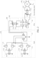
- FIG. 1 is a diagram illustrating a wireless communication device such as a multi-band transceiver 10 (e.g. a Wi-Fi transceiver) according to an embodiment of the present invention.
- the multi-band transceiver 10 may comprise a radio frequency (RF) front-end circuit 100, external front-end modules (eFEMs) 20 and 30, antennas 40 and 50, and a diplexer 60.
- the eFEM 20 may comprise an external low noise amplifier (LNA) 21, an external power amplifier (PA) 22 and a transmitting/receiving (T/R) switch 23.
- the eFEM 30 may comprise an external LNA 31, an external PA 32 and a T/R switch 33.
- the antenna 40 and the eFEM 20 may be configured to receive and transmit RF signals in a first frequency band such as a 2.4 gigahertz (GHz) frequency band
- the antenna 50 and the eFEM 30 may be configured to receive and transmit RF signals in a second frequency band such as a 5 GHz frequency band and a 6 GHz frequency band.
- the diplexer 60 may select the RF signal received by the antenna 40 and the eFEM 20 to be transmitted to the RF front-end circuit 100.
- the diplexer 60 may select the RF signal received by the antenna 50 and the eFEM 30 to be transmitted to the RF front-end circuit 100.
- the antenna 50 and the eFEM 30 support operations of handling the RF signals in both the 5 GHz frequency band and the 6 GHz frequency band, but the present invention is not limited thereto.
- the RF signals in the 5 GHz frequency band and the RF signals in the 6 GHz frequency band may be handled by separated antennas and eFEMs and different modes (e.g. by a 5 G mode and a 6 G mode respectively).
- a number of sets of antennas and eFEMs and a number of modes for different frequency bands are not limited by the scheme shown in FIG. 1 , where those skilled in this art should understand how to extend the number of sets of antennas and eFEMs and the number of modes for different frequency bands according to the scheme shown in FIG. 1 .
- the RF front-end circuit 100 may comprises a receiving amplifier such as a LNA 110, a down-converter such as a down-converting mixer 120, a baseband circuit 130, a baseband circuit 140, an up-converter such as an up-converting mixer 150, a transmitting amplifier such as a programmable gain amplifier (PGA) 160, an output driver such as a PA driver (PAD) 170, and a local oscillation (LO) generator 180 (which may comprise a phase locked loop).
- PGA programmable gain amplifier
- PA driver PA driver
- LO local oscillation
- the down-converting mixer 120 is coupled to the LNA 110
- the baseband circuit 130 is coupled to the down-converting mixer 120
- the up-converting mixer 150 is coupled to the baseband circuit 140
- the PGA 160 is coupled to the up-converting mixer 150
- the PAD 170 is coupled to the PGA 160
- the LO generator 180 is coupled to the down-converting mixer 120 and the up-converting mixer 150.
- the LNA 110 is configured to amplify a RF received signal S RX from the diplexer 60 (e.g. the RF signal received by the antenna 40 and the eFEM 20 or the RF signal received by the antenna 50 and the eFEM 20) to generate an amplified received signal S1 RX .
- the down-converting mixer 120 is configured to down-convert the amplified received signal S1 RX according to a LO signal S LO from the LO generator 180 to generate a down-converted received signal S2 RX .
- the baseband circuit 130 may perform some post-processing such as filtering upon the down-converted received signal S2 RX for backend operations, but the present invention is not limited thereto.
- the up-converting mixer 150 is configured to up-convert a transmitted signal S1 TX from the baseband circuit 140 according to the LO signal S LO to generate an up-converted transmitted signal S2 TX .
- the PGA 160 is configured to amplify the up-converted transmitted signal S2 TX to generate an amplified transmitted signal S3 TX .
- the PAD 170 is configured to output a driving transmitted signal (e.g. a driving transmitted signal S TX1 for driving the external PA 22 or a driving transmitted signal S TX2 for driving the external PA 32) according to the amplified transmitted signal S3 TX .
- a driving transmitted signal e.g. a driving transmitted signal S TX1 for driving the external PA 22 or a driving transmitted signal S TX2 for driving the external PA 32
- At least one of the LNA 110, the up-converting mixer 150 and the PGA 160 may comprise a transformer load, and the transformer load may comprise a switchable inductor.
- the LO signal S LO is set to have a first frequency
- the switchable inductor is set to have a first inductance.
- the LO signal S LO is set to have a second frequency (which is different from the first frequency)
- the switchable inductor is set to have a second inductance (which is different from the first inductance).
- the transformer load and the switchable inductor therein will be described later.
- the PAD 170 may comprise a transconductance stage 171 and output stages 172 and 173, where both of the output stages 172 and 173 are coupled to the transconductance stage 171.
- the transconductance stage 171 is configured to receive the amplified transmitted signal S3 TX from the PGA 160 and generate an output current according to the transmitted signal S3 TX .
- the output stage 172 is implemented according to requirements of the first mode, and is configured to output the driving transmitted signal S TX1 according to the amplified transmitted signal S3 TX (e.g. according to the output current from the transconductance stage 171) when the multi-band transceiver 10 is set to operate in the first mode.
- the output stage 173 is implemented according to requirements of the second mode, and is configured to output the driving transmitted signal S TX2 according to the amplified transmitted signal S3 TX (e.g. according to the output current from the transconductance stage 171) when the multi-band transceiver 10 is set to operate in the second mode.
- a number of output stages is not limited to that in this embodiment, where the number of output stages may vary according to the number of modes for different frequency bands, and each output stage may be implemented according to requirements of respective frequency bands.
- the LNA 110, the down-converting mixer 120 and the baseband circuit 130 belong to a receiving path of the RF front-end circuit 100, and the baseband circuit 140, the up-converting mixer 150, the PGA 160 and the PAD 170 belong to a transmitting path of the RF front-end circuit 100.
- both the receiving path and the transmitting path are implemented to enable the RF front-end circuit 100 be applicable to the multi-band transceiver.
- the receiving path may be omitted, and the RF front-end circuit 100 without the receiving path is applicable to a multi-band transmitter, where at least one of the up-converting mixer 150 and the PGA 160 may comprise the transformer load mentioned above.
- the transmitting path may be omitted, and the RF front-end circuit 100 without the transmitting path is applicable to a multi-band receiver, where the LNA 110 may comprise the transformer load mentioned above.
- the present invention is aimed at mode switching of the LNA 110, the up-converting mixer 150, the PGA 160 and the PAD 170 when the multi-band transceiver 10 is set to operate in either the first mode or the second mode.
- Other implementation details of the multi-band transceiver 10 e.g. the operations of the baseband circuits 130 and 140
- the operations of the baseband circuits 130 and 140 should be well known by those skilled in this art, and will not be described in detail here for brevity.
- FIG. 2 is a diagram illustrating details of some sub-circuits (e.g. the up-converting mixer 150, the PGA 160 and the PAD 170) of the transmitting path of the multi-band transceiver 10 shown in FIG. 1 according to an embodiment of the present invention.
- the up-converting mixer 150 may comprise an up-converting core circuit 151 and a transformer load 152 (which is configured to transform an output impedance of the up-converting mixer 150), where the transformer load 152 is coupled to output terminals of the up-converting core circuit 151.
- the transformer load 152 may comprise inductors L1 MIX and L2 MIX , where the inductor L1 MIX is coupled to the output terminals of the up-converting core circuit 151, and the inductor L2 MIX is coupled to input terminals of the PGA 160.
- the inductors L1 MIX and L2 MIX may be routed concentrically.
- the inductor L2 MIX may represent the switchable inductor (e.g. the inductor L1 MIX has a fixed inductance and the inductor L2 MIX has a switchable inductance).
- the inductor L1 MIX may represent the switchable inductor (e.g. the inductor L2 MIX has a fixed inductance and the inductor L1 MIX has a switchable inductance).
- the PGA 160 may comprise an amplifier core circuit 161 and a transformer load 162 (which is configured to transform an output impedance of the PGA 160), where the transformer load 162 is coupled to output terminals of the amplifier core circuit 161.
- the amplifier core circuit 161 may comprise input transistors such as N-type transistors M1 and M2, and cascaded transistors such as N-type transistors M3 and M4, where gate electrodes of the N-type transistors M1 and M2 may be the input terminals of the PGA 160, and drain terminals of the N-type transistors M3 and M4 may be output terminals of the amplifier core circuit 161.
- the transformer load 162 may comprise inductors L1 PGA and L2 PGA , where the inductor L1 PGA is coupled to the output terminals of the amplifier core circuit 161, and the inductor L2 PGA is coupled to input terminals of the PAD 170.
- the inductors L1 PGA and L2 PGA may be routed concentrically.
- the inductor L2 PGA may represent the switchable inductor (e.g. the inductor L1 PGA has a fixed inductance and the inductor L2 PGA has a switchable inductance).
- the inductor L1 PGA may represent the switchable inductor (e.g. the inductor L2 PGA has a fixed inductance and the inductor L1 PGA has a switchable inductance).
- the transconductance stage 171 may comprise input transistors such as N-type transistors M5 and M6, where gate electrodes of the N-type transistors M5 and M6 may be the input terminals of the PAD 170.
- the output stage 172 may comprise cascaded transistors such as N-type transistors M7 and M8, and a transformer load 172T (which is configured to perform a single-to-differential transformation to output the driving transmitted signal S TX1 shown in FIG. 1 ), where the transformer load 172T may comprise inductors L11 and L12 that are routed concentrically.
- the output stage 173 may comprise cascaded transistors such as N-type transistors M9 and M10, and a transformer load 173T (which is configured to perform a single-to-differential transformation to output the driving transmitted signal S TX2 shown in FIG. 1 ), where the transformer load 173T may comprise inductors L21 and L22 that are routed concentrically.
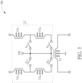
- FIG. 3 is a diagram illustrating a transformer load 300 having a switchable inductor according to an embodiment of the present invention.
- the transformer load 300 may comprise a fixed inductor such as an inductor L1 and the switchable inductor such as an inductor L2.
- the inductor L2 may comprise a first negative sub-inductor such as a sub-inductor L2 N1 , a first positive sub-inductor such as a sub-inductor L2 P1 , a second negative sub-inductor such as a sub-inductor L2 N2 , a second positive sub-inductor such as a sub-inductor L2 P2 , a first negative switch such as a switch S N1 , a first positive switch such as a switch S P1 , a second negative switch such as a switch S N2 , and a second positive switch such as a switch S P2 .
- a first end of the sub-inductor L2 N2 (e.g. an upper end thereof shown in FIG.
- the switch S N1 is coupled between the first end of the sub-inductor L2 N2 and a reference voltage VB
- the switch S P1 is coupled between the first end of the sub-inductor L2 P2 and the reference voltage VB
- the switch S N2 is coupled between a second end of the sub-inductor L2 N2 (e.g.
- the switch S P2 is coupled between a second end of the sub-inductor L2 P2 (e.g. a lower end thereof shown in FIG. 3 ) and the reference voltage VB.
- the transformer load 152 shown in FIG. 2 may be implemented by the transformer load 300.
- the inductor L1 may be coupled to the output terminals of the up-converting core circuit 151
- the inductor L2 may be coupled to the input terminals of the PGA 160 via a second end of the sub-inductor L2 N1 (e.g. an upper end thereof shown in FIG. 3 ) and a second end of the sub-inductor L2 P1 (e.g. an upper end thereof shown in FIG. 3 ).
- the inductor L1 may be coupled to the input terminals of the PGA 160, and the inductor L2 may be coupled to the output terminals of the up-converting core circuit 151 via the second end of the sub-inductor L2 N1 and the second end of the sub-inductor L2 P1 .
- the transformer load 162 shown in FIG. 2 may be implemented by the transformer load 300.
- the inductor L1 may be coupled to the output terminals of the amplifier core circuit 161, and the inductor L2 may be coupled to the input terminals of the PAD 170 via the second end of the sub-inductor L2 N1 and the second end of the sub-inductor L2 P1 .
- the inductor L1 may be coupled to the input terminals of the PAD 170
- the inductor L2 may be coupled to the output terminals of the amplifier core circuit 161 via the second end of the sub-inductor L2 N1 and the second end of the sub-inductor L2 P1 .
- the transformer load 300 shown in FIG. 3 illustrates the mode switching of two modes (e.g. the first mode and the second mode).
- the inductor L2 of the transformer load 300 may further comprise other sub-inductors and switches to make the inductor L2 have three or more different candidate inductances when the multi-band transceiver 10 has three or more modes for three or more different frequency bands.
- Those skilled in this art should understand how to design the transformer load 300 supporting three or more different frequency bands according to the embodiment of FIG. 3 , and related details are omitted here for brevity.
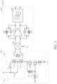
- FIG. 4 is a diagram illustrating details of some sub-circuits (e.g. the LNA 110, the down-converting mixer 120 and the baseband circuit 130) of the receiving path of the RF front-end circuit 100 shown in FIG. 1 according to an embodiment of the present invention.
- the baseband circuit 130 may comprise an in-phase-channel (I-channel) baseband circuit 130-I and a quadrature-channel (Q-channel) baseband circuit 130-Q, where each of the I-channel baseband circuit 130-I and the Q-channel baseband circuit 130-Q may comprise a channel filter (which is formed by an operational amplifier 131, resistors R1 and R2, and capacitors C1 and C2) and a low pass filter 132.
- the channel filter (which is formed by the operational amplifier 131, the resistors R1 and R2, and the capacitors C1 and C2) and the low pass filter 132 should be well known by those skilled in this art, and will not be described in detail here for brevity.
- the LNA 110 may comprise an amplifier core circuit 111 and a transformer load 112.
- the amplifier core circuit 111 may comprise an input transistor such as an N-type transistor M11, a cascaded transistor such as an N-type transistor M12, an input inductor such as an inductor L G , a source inductor such as an inductor L S , a feedback resistor such as a resistor R LNA and a feedback capacitor such as a capacitor C LNA .
- the transformer load 112 may comprise a first inductor such as an inductor L LNA1 and a second inductor such as an inductor L LNA2 .
- the inductor L LNA1 is coupled to an output terminal of the amplifier core circuit 111 (e.g. a drain electrode of the transistor M12), and the inductor L LNA2 is coupled to input terminals of the down-converting mixer 120, where the inductor L LNA1 may be a switchable inductor.
- the inductor L LNA1 may comprise a first sub-inductor such as a sub-inductor L LNA11 , a first switch such as a switch S LD1 , a second sub-inductor such as a sub-inductor L LNA12 , and a second switch such as a switch S LD2 .
- a first end of the sub-inductor L LNA11 (e.g. a lower end thereof shown in FIG. 4 ) is coupled to the output terminal of the amplifier core circuit 111 (e.g. the drain electrode of the transistor M12), and a first end of the sub-inductor L LNA12 (e.g. a lower end thereof shown in FIG.
- the switch S LD1 is coupled between a reference voltage (e.g. a supply voltage) and the second end of the sub-inductor L LNA11
- the switch S LD2 is coupled between the reference voltage (e.g. the supply voltage) and a second end of the sub-inductor L LNA12 .
- the transformer load 112 shown in FIG. 4 illustrates the mode switching of two modes (e.g. the first mode and the second mode).
- the inductor L LNA1 of the transformer load 112 may further comprise other sub-inductors and switches to make the inductor L LNA1 have three or more different candidate inductances when the multi-band transceiver 10 has three or more modes for three or more different frequency bands.
- Those skilled in this art should understand how to design the transformer load 112 supporting three or more different frequency bands according to the embodiment of FIG. 4 , and related details are omitted here for brevity.
- the multi-band transceiver 10 (e.g. the RF front-end circuit 100 therein) can make any or each of the LNA 110, the up-converting mixer 150 and the PGA 160 comprises a switchable transformer load (e.g. a transformer load which comprises at least one switchable inductor), to allow the LNA 110, the up-converting mixer 150 and the PGA 160 properly operate in different modes of the multi-band transceiver 10.
- a switchable transformer load e.g. a transformer load which comprises at least one switchable inductor
- the present invention may also be defined by the following numbered clauses.
Landscapes
- Engineering & Computer Science (AREA)
- Computer Networks & Wireless Communication (AREA)
- Signal Processing (AREA)
- Transceivers (AREA)
- Superheterodyne Receivers (AREA)
Abstract
A radio frequency (RF) front-end circuit of a wireless communication device is provided. The RF front-end circuit includes a receiving amplifier, a down-converter, an up-converter, a transmitting amplifier and an output driver, where the receiving amplifier and the down-converter are configured to process received signals according to a local oscillation (LO) signal, and the up-converter, the transmitting amplifier and the output driver are configured to process transmitted signals according to the LO signal. The receiving amplifier, the up-converter or the transmitting amplifier includes a transformer load. The transformer load includes a switchable inductor. When the wireless communication device operates in a first mode, the LO signal has a first frequency, and the switchable inductor has a first inductance. When the wireless communication device operates in a second mode, the LO signal has a second frequency, and the switchable inductor has a second inductance.
Description
- This application claims the benefit of
U.S. Provisional Application No. 63/439,159, filed on January 16th, 2023 - The present invention is related to multi-band communications devices, and more particularly, to a radio frequency (RF) front-end circuit of a wireless communication device (e.g. a multi-band transceiver, a multi-band transmitter or a multi-band receiver).
- In comparison with Wi-Fi 6 standard, Wi-Fi 7 standard supports wider bandwidth, more operating channels, greater flexibility for channel bandwidth configurations and more complex modulation scheme. For a transceiver of a related art, different modes corresponding to different frequency bands are executed by different circuits. Based on this implementation, when a number of available frequency bands increases, hardware costs of enabling the transceiver to support these frequency bands greatly increases.
- Thus, there is a need for a novel architecture of a transceiver, a transmitter or a receiver supporting multi-band applications, which can be implemented by less hardware costs in comparison with the related art.
- An objective of the present invention is to provide a radio frequency (RF) front-end circuit of a wireless communication device (e.g. a multi-band transceiver, a multi-band transmitter or a multi-band receiver), which can reduce required hardware costs as much as possible, to thereby solve the problem of the related art.
- At least one embodiment of the present invention provides a RF front-end circuit of a wireless communication device. The RF front-end circuit comprises a receiving amplifier, a down-converter, an up-converter, a transmitting amplifier and an output driver, where the down-converter is coupled to the receiving amplifier, the transmitting amplifier is coupled to the up-converter, and the output driver is coupled to the transmitting amplifier. The receiving amplifier is configured to amplify a RF received signal to generate an amplified received signal. The down-converter is configured to down-convert the amplified received signal according to a local oscillation (LO) signal to generate a down-converted received signal. The up-converter is configured to up-convert a transmitted signal according to the LO signal to generate an up-converted transmitted signal. The transmitting amplifier is configured to amplify the up-converted transmitted signal to generate an amplified transmitted signal. The output driver is configured to output a driving transmitted signal according to the amplified transmitted signal. More particularly, at least one of the receiving amplifier, the up-converter and the transmitting amplifier comprises a transformer load, and the transformer load comprises a switchable inductor. When the wireless communication device is set to operate in a first mode, the LO signal is set to have a first frequency, and the switchable inductor is set to have a first inductance. When the wireless communication device is set to operate in a second mode, the LO signal is set to have a second frequency, and the switchable inductor is set to have a second inductance.
- At least one embodiment of the present invention provides a RF front-end circuit of a wireless communication device. The RF front-end circuit comprises an up-converter, a transmitting amplifier and an output driver, where the transmitting amplifier is coupled to the up-converter, and the output driver is coupled to the transmitting amplifier. The up-converter is configured to up-convert a transmitted signal according to a LO signal to generate an up-converted transmitted signal. The transmitting amplifier is configured to amplify the up-converted transmitted signal to generate an amplified transmitted signal. The output driver is configured to output a driving transmitted signal according to the amplified transmitted signal. More particularly, at least one of the up-converter and the transmitting amplifier comprises a transformer load, and the transformer load comprises a switchable inductor. When the wireless communication device is set to operate in a first mode, the LO signal is set to have a first frequency, and the switchable inductor is set to have a first inductance. When the wireless communication device is set to operate in a second mode, the LO signal is set to have a second frequency, and the switchable inductor is set to have a second inductance.
- At least one embodiment of the present invention provides a RF front-end circuit of a wireless communication device. The RF front-end circuit comprises a receiving amplifier and a down-converter, where the down-converter is coupled to the receiving amplifier. The receiving amplifier is configured to amplify a RF received signal to generate an amplified received signal. The down-converter is configured to down-convert the amplified received signal according to a LO signal to generate a down-converted received signal More particularly, the receiving amplifier comprises a transformer load, and the transformer load comprises a switchable inductor. When the wireless communication device is set to operate in a first mode, the LO signal is set to have a first frequency, and the switchable inductor is set to have a first inductance. When the wireless communication device is set to operate in a second mode, the LO signal is set to have a second frequency, and the switchable inductor is set to have a second inductance.
- The RF front-end circuit provided by the embodiments of the present invention can make at least one inductor within the transformer load of the receiving amplifier (e.g. a low noise amplifier), the up-converter (e.g. a mixer for up-conversion) and the transmitting amplifier (e.g. a programmable gain amplifier) be switchable, thereby enabling the receiving amplifier, the up-converter and the transmitting amplifier be utilized in both a transmitting mode and a receiving mode. Thus, the transmitting mode and the receiving mode can share the hardware of the receiving amplifier, the up-converter and the transmitting amplifier.
- These and other objectives of the present invention will no doubt become obvious to those of ordinary skill in the art after reading the following detailed description of the preferred embodiment that is illustrated in the various figures and drawings.
-
-
FIG. 1 is a diagram illustrating a wireless communication device according to an embodiment of the present invention. -
FIG. 2 is a diagram illustrating details of some sub-circuits of a transmitting path of a radio frequency (RF) front-end circuit shown inFIG. 1 according to an embodiment of the present invention. -
FIG. 3 is a diagram illustrating a transformer load having a switchable inductor according to an embodiment of the present invention. -
FIG. 4 is a diagram illustrating details of some sub-circuits of a receiving path of the RF front-end circuit shown inFIG. 1 according to an embodiment of the present invention. - Certain terms are used throughout the following description and claims, which refer to particular components. As one skilled in the art will appreciate, electronic equipment manufacturers may refer to a component by different names. This document does not intend to distinguish between components that differ in name but not in function. In the following description and in the claims, the terms "include" and "comprise" are used in an open-ended fashion, and thus should be interpreted to mean "include, but not limited to ...". Also, the term "couple" is intended to mean either an indirect or direct electrical connection. Accordingly, if one device is coupled to another device, that connection may be through a direct electrical connection, or through an indirect electrical connection via other devices and connections.
-
FIG. 1 is a diagram illustrating a wireless communication device such as a multi-band transceiver 10 (e.g. a Wi-Fi transceiver) according to an embodiment of the present invention. As shown inFIG. 1 , themulti-band transceiver 10 may comprise a radio frequency (RF) front-end circuit 100, external front-end modules (eFEMs) 20 and 30,antennas diplexer 60. TheeFEM 20 may comprise an external low noise amplifier (LNA) 21, an external power amplifier (PA) 22 and a transmitting/receiving (T/R)switch 23. TheeFEM 30 may comprise anexternal LNA 31, anexternal PA 32 and a T/R switch 33. In this embodiment, theantenna 40 and the eFEM 20 may be configured to receive and transmit RF signals in a first frequency band such as a 2.4 gigahertz (GHz) frequency band, and theantenna 50 and the eFEM 30 may be configured to receive and transmit RF signals in a second frequency band such as a 5 GHz frequency band and a 6 GHz frequency band. When themulti-band transceiver 10 is set to operate in a first mode such as a 2.4 GHz mode, thediplexer 60 may select the RF signal received by theantenna 40 and the eFEM 20 to be transmitted to the RF front-end circuit 100. When themulti-band transceiver 10 is set to operate in a second mode such as a 5/6 GHz mode, thediplexer 60 may select the RF signal received by theantenna 50 and the eFEM 30 to be transmitted to the RF front-end circuit 100. - In this embodiment, the
antenna 50 and the eFEM 30 support operations of handling the RF signals in both the 5 GHz frequency band and the 6 GHz frequency band, but the present invention is not limited thereto. In some embodiment, the RF signals in the 5 GHz frequency band and the RF signals in the 6 GHz frequency band may be handled by separated antennas and eFEMs and different modes (e.g. by a 5 G mode and a 6 G mode respectively). In addition, a number of sets of antennas and eFEMs and a number of modes for different frequency bands are not limited by the scheme shown inFIG. 1 , where those skilled in this art should understand how to extend the number of sets of antennas and eFEMs and the number of modes for different frequency bands according to the scheme shown inFIG. 1 . - In this embodiment, the RF front-
end circuit 100 may comprises a receiving amplifier such as aLNA 110, a down-converter such as a down-converting mixer 120, abaseband circuit 130, abaseband circuit 140, an up-converter such as an up-convertingmixer 150, a transmitting amplifier such as a programmable gain amplifier (PGA) 160, an output driver such as a PA driver (PAD) 170, and a local oscillation (LO) generator 180 (which may comprise a phase locked loop). As shown inFIG. 1 , the down-convertingmixer 120 is coupled to theLNA 110, thebaseband circuit 130 is coupled to the down-convertingmixer 120, the up-convertingmixer 150 is coupled to thebaseband circuit 140, thePGA 160 is coupled to the up-convertingmixer 150, thePAD 170 is coupled to thePGA 160, and theLO generator 180 is coupled to the down-convertingmixer 120 and the up-convertingmixer 150. - In this embodiment, the LNA 110 is configured to amplify a RF received signal SRX from the diplexer 60 (e.g. the RF signal received by the
antenna 40 and theeFEM 20 or the RF signal received by theantenna 50 and the eFEM 20) to generate an amplified received signal S1RX. The down-convertingmixer 120 is configured to down-convert the amplified received signal S1RX according to a LO signal SLO from theLO generator 180 to generate a down-converted received signal S2RX. Thebaseband circuit 130 may perform some post-processing such as filtering upon the down-converted received signal S2RX for backend operations, but the present invention is not limited thereto. The up-convertingmixer 150 is configured to up-convert a transmitted signal S1TX from thebaseband circuit 140 according to the LO signal SLO to generate an up-converted transmitted signal S2TX. ThePGA 160 is configured to amplify the up-converted transmitted signal S2TX to generate an amplified transmitted signal S3TX. ThePAD 170 is configured to output a driving transmitted signal (e.g. a driving transmitted signal STX1 for driving the external PA 22 or a driving transmitted signal STX2 for driving the external PA 32) according to the amplified transmitted signal S3TX. - In this embodiment, at least one of the
LNA 110, the up-convertingmixer 150 and thePGA 160 may comprise a transformer load, and the transformer load may comprise a switchable inductor. When themulti-band transceiver 10 is set to operate in the first mode (e.g. the 2.4 GHz mode), the LO signal SLO is set to have a first frequency, and the switchable inductor is set to have a first inductance. When themulti-band transceiver 10 is set to operate in the second mode (e.g. the 5/6 GHz mode), the LO signal SLO is set to have a second frequency (which is different from the first frequency), and the switchable inductor is set to have a second inductance (which is different from the first inductance). Detailed implementation of the transformer load and the switchable inductor therein will be described later. - In this embodiment, the
PAD 170 may comprise atransconductance stage 171 andoutput stages transconductance stage 171. Thetransconductance stage 171 is configured to receive the amplified transmitted signal S3TX from thePGA 160 and generate an output current according to the transmitted signal S3TX. Theoutput stage 172 is implemented according to requirements of the first mode, and is configured to output the driving transmitted signal STX1 according to the amplified transmitted signal S3TX (e.g. according to the output current from the transconductance stage 171) when themulti-band transceiver 10 is set to operate in the first mode. Theoutput stage 173 is implemented according to requirements of the second mode, and is configured to output the driving transmitted signal STX2 according to the amplified transmitted signal S3TX (e.g. according to the output current from the transconductance stage 171) when themulti-band transceiver 10 is set to operate in the second mode. It should be noted that a number of output stages is not limited to that in this embodiment, where the number of output stages may vary according to the number of modes for different frequency bands, and each output stage may be implemented according to requirements of respective frequency bands. - The
LNA 110, the down-convertingmixer 120 and thebaseband circuit 130 belong to a receiving path of the RF front-end circuit 100, and thebaseband circuit 140, the up-convertingmixer 150, thePGA 160 and thePAD 170 belong to a transmitting path of the RF front-end circuit 100. In this embodiment, both the receiving path and the transmitting path are implemented to enable the RF front-end circuit 100 be applicable to the multi-band transceiver. In some embodiment, the receiving path may be omitted, and the RF front-end circuit 100 without the receiving path is applicable to a multi-band transmitter, where at least one of the up-convertingmixer 150 and thePGA 160 may comprise the transformer load mentioned above. In some embodiment, the transmitting path may be omitted, and the RF front-end circuit 100 without the transmitting path is applicable to a multi-band receiver, where theLNA 110 may comprise the transformer load mentioned above. - It should be noted that the present invention is aimed at mode switching of the
LNA 110, the up-convertingmixer 150, thePGA 160 and thePAD 170 when themulti-band transceiver 10 is set to operate in either the first mode or the second mode. Other implementation details of the multi-band transceiver 10 (e.g. the operations of thebaseband circuits 130 and 140) that is unrelated to the mode switching mentioned above should be well known by those skilled in this art, and will not be described in detail here for brevity. -
FIG. 2 is a diagram illustrating details of some sub-circuits (e.g. the up-convertingmixer 150, thePGA 160 and the PAD 170) of the transmitting path of themulti-band transceiver 10 shown inFIG. 1 according to an embodiment of the present invention. As shown inFIG. 2 , the up-convertingmixer 150 may comprise an up-convertingcore circuit 151 and a transformer load 152 (which is configured to transform an output impedance of the up-converting mixer 150), where thetransformer load 152 is coupled to output terminals of the up-convertingcore circuit 151. Thetransformer load 152 may comprise inductors L1MIX and L2MIX, where the inductor L1MIX is coupled to the output terminals of the up-convertingcore circuit 151, and the inductor L2MIX is coupled to input terminals of thePGA 160. The inductors L1MIX and L2MIX may be routed concentrically. In this embodiment, the inductor L2MIX may represent the switchable inductor (e.g. the inductor L1MIX has a fixed inductance and the inductor L2MIX has a switchable inductance). In some embodiment, the inductor L1MIX may represent the switchable inductor (e.g. the inductor L2MIX has a fixed inductance and the inductor L1MIX has a switchable inductance). - In this embodiment, the
PGA 160 may comprise anamplifier core circuit 161 and a transformer load 162 (which is configured to transform an output impedance of the PGA 160), where thetransformer load 162 is coupled to output terminals of theamplifier core circuit 161. Theamplifier core circuit 161 may comprise input transistors such as N-type transistors M1 and M2, and cascaded transistors such as N-type transistors M3 and M4, where gate electrodes of the N-type transistors M1 and M2 may be the input terminals of thePGA 160, and drain terminals of the N-type transistors M3 and M4 may be output terminals of theamplifier core circuit 161. Thetransformer load 162 may comprise inductors L1PGA and L2 PGA, where the inductor L1PGA is coupled to the output terminals of theamplifier core circuit 161, and the inductor L2PGA is coupled to input terminals of thePAD 170. The inductors L1PGA and L2PGA may be routed concentrically. In this embodiment, the inductor L2PGA may represent the switchable inductor (e.g. the inductor L1PGA has a fixed inductance and the inductor L2PGA has a switchable inductance). In some embodiment, the inductor L1PGA may represent the switchable inductor (e.g. the inductor L2PGA has a fixed inductance and the inductor L1PGA has a switchable inductance). - In this embodiment, the
transconductance stage 171 may comprise input transistors such as N-type transistors M5 and M6, where gate electrodes of the N-type transistors M5 and M6 may be the input terminals of thePAD 170. Theoutput stage 172 may comprise cascaded transistors such as N-type transistors M7 and M8, and a transformer load 172T (which is configured to perform a single-to-differential transformation to output the driving transmitted signal STX1 shown inFIG. 1 ), where the transformer load 172T may comprise inductors L11 and L12 that are routed concentrically. In addition, theoutput stage 173 may comprise cascaded transistors such as N-type transistors M9 and M10, and a transformer load 173T (which is configured to perform a single-to-differential transformation to output the driving transmitted signal STX2 shown inFIG. 1 ), where the transformer load 173T may comprise inductors L21 and L22 that are routed concentrically. -
FIG. 3 is a diagram illustrating atransformer load 300 having a switchable inductor according to an embodiment of the present invention. In this embodiment, thetransformer load 300 may comprise a fixed inductor such as an inductor L1 and the switchable inductor such as an inductor L2. The inductor L2 may comprise a first negative sub-inductor such as a sub-inductor L2N1, a first positive sub-inductor such as a sub-inductor L2P1, a second negative sub-inductor such as a sub-inductor L2N2, a second positive sub-inductor such as a sub-inductor L2P2, a first negative switch such as a switch SN1, a first positive switch such as a switch SP1, a second negative switch such as a switch SN2, and a second positive switch such as a switch SP2. A first end of the sub-inductor L2N2 (e.g. an upper end thereof shown inFIG. 3 ) is coupled to a first end of the sub-inductor L2N1 (e.g. a lower end thereof shown inFIG. 3 ), and a first end of the sub-inductor L2P2 (e.g. an upper end thereof shown inFIG. 3 ) is coupled to a first end of the sub-inductor L2P1 (e.g. a lower end thereof shown inFIG. 3 ). The switch SN1 is coupled between the first end of the sub-inductor L2N2 and a reference voltage VB, the switch SP1 is coupled between the first end of the sub-inductor L2P2 and the reference voltage VB, the switch SN2 is coupled between a second end of the sub-inductor L2N2 (e.g. a lower end thereof shown inFIG. 3 ) and the reference voltage VB, and the switch SP2 is coupled between a second end of the sub-inductor L2P2 (e.g. a lower end thereof shown inFIG. 3 ) and the reference voltage VB. When themulti-band transceiver 10 is set to operate in the first mode, the switches SN1 and SP1 are turned off, and the switches SN2 and SP2 are turned on, making L2 = L2N1 + L2N2 + L2P1 + L2P2. When themulti-band transceiver 10 is set to operate in the second mode, the switches SN1 and SP1 are turned on, and the switches SN2 and SP2 are turned off, making L2 = L2N1 + L2P1. - In one embodiment, the
transformer load 152 shown inFIG. 2 may be implemented by thetransformer load 300. For example, the inductor L1 may be coupled to the output terminals of the up-convertingcore circuit 151, and the inductor L2 may be coupled to the input terminals of thePGA 160 via a second end of the sub-inductor L2N1 (e.g. an upper end thereof shown inFIG. 3 ) and a second end of the sub-inductor L2P1 (e.g. an upper end thereof shown inFIG. 3 ). In another example, the inductor L1 may be coupled to the input terminals of thePGA 160, and the inductor L2 may be coupled to the output terminals of the up-convertingcore circuit 151 via the second end of the sub-inductor L2N1 and the second end of the sub-inductor L2P1. - In one embodiment, the
transformer load 162 shown inFIG. 2 may be implemented by thetransformer load 300. For example, the inductor L1 may be coupled to the output terminals of theamplifier core circuit 161, and the inductor L2 may be coupled to the input terminals of thePAD 170 via the second end of the sub-inductor L2N1 and the second end of the sub-inductor L2P1. In another example, the inductor L1 may be coupled to the input terminals of thePAD 170, and the inductor L2 may be coupled to the output terminals of theamplifier core circuit 161 via the second end of the sub-inductor L2N1 and the second end of the sub-inductor L2P1. - The
transformer load 300 shown inFIG. 3 illustrates the mode switching of two modes (e.g. the first mode and the second mode). In some embodiment, the inductor L2 of thetransformer load 300 may further comprise other sub-inductors and switches to make the inductor L2 have three or more different candidate inductances when themulti-band transceiver 10 has three or more modes for three or more different frequency bands. Those skilled in this art should understand how to design thetransformer load 300 supporting three or more different frequency bands according to the embodiment ofFIG. 3 , and related details are omitted here for brevity. -
FIG. 4 is a diagram illustrating details of some sub-circuits (e.g. theLNA 110, the down-convertingmixer 120 and the baseband circuit 130) of the receiving path of the RF front-end circuit 100 shown inFIG. 1 according to an embodiment of the present invention. In this embodiment, thebaseband circuit 130 may comprise an in-phase-channel (I-channel) baseband circuit 130-I and a quadrature-channel (Q-channel) baseband circuit 130-Q, where each of the I-channel baseband circuit 130-I and the Q-channel baseband circuit 130-Q may comprise a channel filter (which is formed by anoperational amplifier 131, resistors R1 and R2, and capacitors C1 and C2) and alow pass filter 132. The channel filter (which is formed by theoperational amplifier 131, the resistors R1 and R2, and the capacitors C1 and C2) and thelow pass filter 132 should be well known by those skilled in this art, and will not be described in detail here for brevity. In addition, theLNA 110 may comprise anamplifier core circuit 111 and atransformer load 112. Theamplifier core circuit 111 may comprise an input transistor such as an N-type transistor M11, a cascaded transistor such as an N-type transistor M12, an input inductor such as an inductor LG, a source inductor such as an inductor LS, a feedback resistor such as a resistor RLNA and a feedback capacitor such as a capacitor CLNA. - In this embodiment, the
transformer load 112 may comprise a first inductor such as an inductor LLNA1 and a second inductor such as an inductor LLNA2. The inductor LLNA1 is coupled to an output terminal of the amplifier core circuit 111 (e.g. a drain electrode of the transistor M12), and the inductor LLNA2 is coupled to input terminals of the down-convertingmixer 120, where the inductor LLNA1 may be a switchable inductor. For example, the inductor LLNA1 may comprise a first sub-inductor such as a sub-inductor LLNA11, a first switch such as a switch SLD1, a second sub-inductor such as a sub-inductor LLNA12, and a second switch such as a switch SLD2. A first end of the sub-inductor LLNA11 (e.g. a lower end thereof shown inFIG. 4 ) is coupled to the output terminal of the amplifier core circuit 111 (e.g. the drain electrode of the transistor M12), and a first end of the sub-inductor LLNA12 (e.g. a lower end thereof shown inFIG. 4 ) is coupled to a second end of the sub-inductor LLNA11 (e.g. an upper end thereof shown inFIG. 4 ). The switch SLD1 is coupled between a reference voltage (e.g. a supply voltage) and the second end of the sub-inductor LLNA11, and the switch SLD2 is coupled between the reference voltage (e.g. the supply voltage) and a second end of the sub-inductor LLNA12. When themulti-band transceiver 10 is set to operate in the first mode, the switch SLD1 is turned off and the switch SLD2 is turned on, making LLNA1 = LLNA11 + LLNA12. When themulti-band transceiver 10 is set to operate in the second mode, the switch SLD1 is turned on and the switch SLD2 is turned off, making LLNA1 = LLNA11. - The
transformer load 112 shown inFIG. 4 illustrates the mode switching of two modes (e.g. the first mode and the second mode). In some embodiment, the inductor LLNA1 of thetransformer load 112 may further comprise other sub-inductors and switches to make the inductor LLNA1 have three or more different candidate inductances when themulti-band transceiver 10 has three or more modes for three or more different frequency bands. Those skilled in this art should understand how to design thetransformer load 112 supporting three or more different frequency bands according to the embodiment ofFIG. 4 , and related details are omitted here for brevity. - To summarize, the multi-band transceiver 10 (e.g. the RF front-
end circuit 100 therein) can make any or each of theLNA 110, the up-convertingmixer 150 and thePGA 160 comprises a switchable transformer load (e.g. a transformer load which comprises at least one switchable inductor), to allow theLNA 110, the up-convertingmixer 150 and thePGA 160 properly operate in different modes of themulti-band transceiver 10. Thus, the embodiment of the present invention does not need to implement separated LNAs, up-converting mixers and/or PGAs for different modes, and an overall circuit area can be reduced. - Those skilled in the art will readily observe that numerous modifications and alterations of the device and method may be made while retaining the teachings of the invention. Accordingly, the above disclosure should be construed as limited only by the metes and bounds of the appended claims.
- The present invention may also be defined by the following numbered clauses.
- 1. A radio frequency (RF) front-end circuit of a wireless communication device, comprising:
- a receiving amplifier, configured to amplify a RF received signal to generate an amplified received signal;
- a down-converter, coupled to the receiving amplifier, configured to down-convert the amplified received signal according to a local oscillation (LO) signal to generate a down-converted received signal;
- an up-converter, configured to up-convert a transmitted signal according to the LO signal to generate an up-converted transmitted signal;
- a transmitting amplifier, coupled to the up-converter, configured to amplify the up-converted transmitted signal to generate an amplified transmitted signal; and
- an output driver, coupled to the transmitting amplifier, configured to output a driving transmitted signal according to the amplified transmitted signal;
- wherein at least one of the receiving amplifier, the up-converter and the transmitting amplifier comprises a transformer load, and the transformer load comprises a switchable inductor; when the wireless communication device is set to operate in a first mode, the LO signal is set to have a first frequency, and the switchable inductor is set to have a first inductance; and when the wireless communication device is set to operate in a second mode, the LO signal is set to have a second frequency, and the switchable inductor is set to have a second inductance.
- 2. The RF front-end circuit of clause 1, wherein the up-converter comprises the transformer load, and the transformer load comprises:
- a first inductor, coupled to output terminals of an up-converting core circuit of the up-converter; and
- a second inductor, coupled to input terminals of the transmitting amplifier;
- wherein one of the first inductor and the second inductor represents the switchable inductor.
- 3. The RF front-end circuit of clause 2, wherein the switchable inductor comprises:
- a first negative sub-inductor;
- a first positive sub-inductor;
- a second negative sub-inductor, wherein a first end of the second negative sub-inductor is coupled to the first negative sub-inductor;
- a second positive sub-inductor, wherein a first end of the second positive sub-inductor is coupled to the first positive sub-inductor;
- a first negative switch, coupled between the first end of the second negative sub-inductor and a reference voltage;
- a first positive switch, coupled between the first end of the second positive sub-inductor and the reference voltage;
- a second negative switch, coupled between a second end of the second negative sub-inductor and the reference voltage; and
- a second positive switch, coupled between a second end of the second positive sub-inductor and the reference voltage;
- wherein:
- when the wireless communication device is set to operate in the first mode, the first negative switch and the first positive switch are turned off, and the second negative switch and the second positive switch are turned on; and
- when the wireless communication device is set to operate in the second mode, the first negative switch and the first positive switch are turned on, and the second negative switch and the second positive switch are turned off.
- 4. The RF front-end circuit of clause 1, wherein the transmitting amplifier comprises the transformer load, and the transformer load comprises:
- a first inductor, coupled to output terminals of an amplifier core circuit of the transmitting amplifier; and
- a second inductor, coupled to input terminals of the output driver;
- wherein one of the first inductor and the second inductor represents the switchable inductor.
- 5. The RF front-end circuit of clause 4, wherein the switchable inductor comprises:
- a first negative sub-inductor;
- a first positive sub-inductor;
- a second negative sub-inductor, wherein a first end of the second negative sub-inductor is coupled to the first negative sub-inductor;
- a second positive sub-inductor, wherein a first end of the second positive sub-inductor is coupled to the first positive sub-inductor;
- a first negative switch, coupled between the first end of the second negative sub-inductor and a reference voltage;
- a first positive switch, coupled between the first end of the second positive sub-inductor and the reference voltage;
- a second negative switch, coupled between a second end of the second negative sub-inductor and the reference voltage; and
- a second positive switch, coupled between a second end of the second positive sub-inductor and the reference voltage;
- wherein:
- when the wireless communication device is set to operate in the first mode, the first negative switch and the first positive switch are turned off, and the second negative switch and the second positive switch are turned on; and
- when the wireless communication device is set to operate in the second mode, the first negative switch and the first positive switch are turned on, and the second negative switch and the second positive switch are turned off.
- 6. The RF front-end circuit of clause 1, wherein the output driver comprises:
- a transconductance stage, configured to receive the amplified transmitted signal from the transmitting amplifier;
- a first output stage, coupled to the transconductance stage, configured to output a first driving transmitted signal according to the amplified transmitted signal when the wireless communication device is set to operate in the first mode; and
- a second output stage, coupled to the transconductance stage, configured to output a second driving transmitted signal according to the amplified transmitted signal when the wireless communication device is set to operate in the second mode;
- wherein the driving transmitted signal comprises the first driving transmitted signal and the second driving transmitted signal.
- 7. The RF front-end circuit of clause 1, wherein the receiving amplifier comprises the transformer load, and the transformer load comprises:
- a first inductor, coupled to an output terminal of an amplifier core circuit of the receiving amplifier; and
- a second inductor, coupled to input terminals of the down-converter;
- wherein the first inductor represents the switchable inductor.
- 8. The RF front-end circuit of clause 7, wherein the switchable inductor comprises:
- a first sub-inductor, wherein a first end of the first sub-inductor is coupled to the output terminal of the amplifier core circuit;
- a first switch, coupled between a reference voltage and a second end of the first sub-inductor;
- a second sub-inductor, wherein a first end of the second sub-inductor is coupled to the second end of the first sub-inductor; and
- a second switch, coupled between the reference voltage and a second end of the second sub-inductor;
- wherein:
- when the wireless communication device is set to operate in the first mode, the first switch is turned off and the second switch is turned on; and
- when the wireless communication device is set to operate in the second mode, the first switch is turned on and the second switch is turned off.
- 9. A radio frequency (RF) front-end circuit of a wireless communication device, comprising:
- an up-converter, configured to up-convert a transmitted signal according to a local oscillation (LO) signal to generate an up-converted transmitted signal;
- a transmitting amplifier, coupled to the up-converter, configured to amplify the up-converted transmitted signal to generate an amplified transmitted signal; and
- an output driver, coupled to the transmitting amplifier, configured to output a driving transmitted signal according to the amplified transmitted signal;
- wherein at least one of the up-converter and the transmitting amplifier comprises a transformer load, and the transformer load comprises a switchable inductor; when the wireless communication device is set to operate in a first mode, the LO signal is set to have a first frequency, and the switchable inductor is set to have a first inductance; and when the wireless communication device is set to operate in a second mode, the LO signal is set to have a second frequency, and the switchable inductor is set to have a second inductance.
- 10. The RF front-end circuit of clause 9, wherein the up-converter comprises the transformer load coupled to output terminals of an up-converting core circuit of the up-converter, and the transformer load comprises:
- a first inductor, coupled to the output terminals of the up-converting core circuit; and
- a second inductor, coupled to input terminals of the transmitting amplifier;
- wherein one of the first inductor and the second inductor represents the switchable inductor.
- 11. The RF front-end circuit of
clause 10, wherein the switchable inductor comprises:- a first negative sub-inductor;
- a first positive sub-inductor;
- a second negative sub-inductor, wherein a first end of the second negative sub-inductor is coupled to the first negative sub-inductor;
- a second positive sub-inductor, wherein a first end of the second positive sub-inductor is coupled to the first positive sub-inductor;
- a first negative switch, coupled between the first end of the second negative sub-inductor and a reference voltage;
- a first positive switch, coupled between the first end of the second positive sub-inductor and the reference voltage;
- a second negative switch, coupled between a second end of the second negative sub-inductor and the reference voltage; and
- a second positive switch, coupled between a second end of the second positive sub-inductor and the reference voltage;
- wherein:
- when the wireless communication device is set to operate in the first mode, the first negative switch and the first positive switch are turned off, and the second negative switch and the second positive switch are turned on; and
- when the wireless communication device is set to operate in the second mode, the first negative switch and the first positive switch are turned on, and the second negative switch and the second positive switch are turned off.
- 12. The RF front-end circuit of clause 9, wherein the transmitting amplifier comprises the transformer load coupled to output terminals of an amplifier core circuit of the transmitting amplifier, and the transformer load comprises:
- a first inductor, coupled to the output terminals of the amplifier core circuit; and
- a second inductor, coupled to input terminals of the output driver;
- wherein one of the first inductor and the second inductor represents the switchable inductor.
- 13. The RF front-end circuit of clause 12, wherein the switchable inductor comprises:
- a first negative sub-inductor;
- a first positive sub-inductor;
- a second negative sub-inductor, wherein a first end of the second negative sub-inductor is coupled to the first negative sub-inductor;
- a second positive sub-inductor, wherein a first end of the second positive sub-inductor is coupled to the first positive sub-inductor;
- a first negative switch, coupled between the first end of the second negative sub-inductor and a reference voltage;
- a first positive switch, coupled between the first end of the second positive sub-inductor and the reference voltage;
- a second negative switch, coupled between a second end of the second negative sub-inductor and the reference voltage; and
- a second positive switch, coupled between a second end of the second positive sub-inductor and the reference voltage;
- wherein:
- when the wireless communication device is set to operate in the first mode, the first negative switch and the first positive switch are turned off, and the second negative switch and the second positive switch are turned on; and
- when the wireless communication device is set to operate in the second mode, the first negative switch and the first positive switch are turned on, and the second negative switch and the second positive switch are turned off.
- 14. The RF front-end circuit of clause 9, wherein the output driver comprises:
- a transconductance stage, configured to receive the amplified transmitted signal from the transmitting amplifier;
- a first output stage, coupled to the transconductance stage, configured to output a first driving transmitted signal according to the amplified transmitted signal when the wireless communication device is set to operate in the first mode; and
- a second output stage, coupled to the transconductance stage, configured to output a second driving transmitted signal according to the amplified transmitted signal when the wireless communication device is set to operate in the second mode;
- wherein the driving transmitted signal comprises the first driving transmitted signal and the second driving transmitted signal.
- 15. A radio frequency (RF) front-end circuit of a wireless communication device, comprising:
- a receiving amplifier, configured to amplify a RF received signal to generate an amplified received signal; and
- a down-converter, coupled to the receiving amplifier, configured to down-convert the amplified received signal according to a local oscillation (LO) signal to generate a down-converted received signal;
- wherein the receiving amplifier comprises a transformer load, and the transformer load comprises a switchable inductor; when the wireless communication device is set to operate in a first mode, the LO signal is set to have a first frequency, and the switchable inductor is set to have a first inductance; and when the wireless communication device is set to operate in a second mode, the LO signal is set to have a second frequency, and the switchable inductor is set to have a second inductance.
- 16. The RF front-end circuit of clause 15, wherein the transformer load comprises:
- a first inductor, coupled to an output terminal of an amplifier core circuit of the receiving amplifier; and
- a second inductor, coupled to input terminals of the down-converter;
- wherein the first inductor represents the switchable inductor.
- 17. The RF front-end circuit of clause 16, wherein the switchable inductor comprises:
- a first sub-inductor, wherein a first end of the first sub-inductor is coupled to the output terminal of the amplifier core circuit;
- a first switch, coupled between a reference voltage and a second end of the first sub-inductor
- a second sub-inductor, wherein a first end of the second sub-inductor is coupled to the second end of the first sub-inductor; and
- a second switch, coupled between the reference voltage and a second end of the second sub-inductor;
- wherein:
- when the wireless communication device is set to operate in the first mode, the first switch is turned off and the second switch is turned on; and
- when the wireless communication device is set to operate in the second mode, the first switch is turned on and the second switch is turned off.
Claims (15)
- A radio frequency, RF, front-end circuit (100) of a wireless communication device, comprising:a receiving amplifier (110), configured to amplify a RF received signal to generate an amplified received signal;a down-converter (120), coupled to the receiving amplifier (110), configured to down-convert the amplified received signal according to a local oscillation, LO, signal to generate a down-converted received signal;an up-converter (150), configured to up-convert a transmitted signal according to the LO signal to generate an up-converted transmitted signal;a transmitting amplifier (160), coupled to the up-converter (150), configured to amplify the up-converted transmitted signal to generate an amplified transmitted signal; andan output driver (170), coupled to the transmitting amplifier (160), configured to output a driving transmitted signal according to the amplified transmitted signal;wherein at least one of the receiving amplifier (110), the up-converter (150) and the transmitting amplifier (160) comprises a transformer load (112, 152, 162, 172t, 173t, 300), and the transformer load (112, 152, 162, 172t, 173t, 300) comprises a switchable inductor; when the wireless communication device is set to operate in a first mode, the LO signal is set to have a first frequency, and the switchable inductor is set to have a first inductance; and when the wireless communication device is set to operate in a second mode, the LO signal is set to have a second frequency, and the switchable inductor is set to have a second inductance.
- The RF front-end circuit (100) of claim 1, wherein the up-converter (150) comprises the transformer load (112, 152, 162, 172t, 173t, 300), and the transformer load (112, 152, 162, 172t, 173t, 300) comprises:a first inductor (LLNA1), coupled to output terminals of an up-converting core circuit (151) of the up-converter (150); anda second inductor (LLNA2), coupled to input terminals of the transmitting amplifier (160);wherein one of the first inductor (LLNA1) and the second inductor (LLNA2) represents the switchable inductor.
- The RF front-end circuit (100) of claim 2, wherein the switchable inductor comprises:a first negative sub-inductor (L2N1);a first positive sub-inductor (L2P1);a second negative sub-inductor (L2N2), wherein a first end of the second negative sub-inductor (L2N2) is coupled to the first negative sub-inductor (L2N1);a second positive sub-inductor (L2P2), wherein a first end of the second positive sub-inductor is coupled to the first positive sub-inductor;a first negative switch (SN1), coupled between the first end of the second negative sub-inductor (L2N2) and a reference voltage;a first positive switch (SP1), coupled between the first end of the second positive sub-inductor and the reference voltage;a second negative switch (SN2), coupled between a second end of the second negative sub-inductor (L2N2) and the reference voltage; anda second positive switch (SP2), coupled between a second end of the second positive sub-inductor and the reference voltage;wherein:when the wireless communication device is set to operate in the first mode, the first negative switch (SN1) and the first positive switch (SP1) are turned off, and the second negative switch and the second positive switch are turned on; andwhen the wireless communication device is set to operate in the second mode, the first negative switch (SN1) and the first positive switch (SP1) are turned on, and the second negative switch and the second positive switch are turned off.
- The RF front-end circuit (100) of claim 1, wherein the transmitting amplifier (160) comprises the transformer load (112, 152, 162, 172t, 173t, 300), and the transformer load (112, 152, 162, 172t, 173t, 300) comprises:a first inductor (LLNA1), coupled to output terminals of an amplifier core circuit (111, 161) of the transmitting amplifier (160); anda second inductor (LLNA2), coupled to input terminals of the output driver (170);wherein one of the first inductor (LLNA1) and the second inductor (LLNA2) represents the switchable inductor.
- The RF front-end circuit (100) of claim 4, wherein the switchable inductor comprises:a first negative sub-inductor (L2N1);a first positive sub-inductor (L2P1);a second negative sub-inductor (L2N2), wherein a first end of the second negative sub-inductor (L2N2) is coupled to the first negative sub-inductor (L2N1);a second positive sub-inductor (L2P2), wherein a first end of the second positive sub-inductor is coupled to the first positive sub-inductor;a first negative switch (SN1), coupled between the first end of the second negative sub-inductor (L2N2) and a reference voltage;a first positive switch (SP1), coupled between the first end of the second positive sub-inductor and the reference voltage;a second negative switch (SN2), coupled between a second end of the second negative sub-inductor (L2N2) and the reference voltage; anda second positive switch (SP2), coupled between a second end of the second positive sub-inductor and the reference voltage;wherein:when the wireless communication device is set to operate in the first mode, the first negative switch (SN1) and the first positive switch (SP1) are turned off, and the second negative switch and the second positive switch are turned on; andwhen the wireless communication device is set to operate in the second mode, the first negative switch (SN1) and the first positive switch (SP1) are turned on, and the second negative switch and the second positive switch are turned off.
- The RF front-end circuit (100) of claim 1, wherein the receiving amplifier (110) comprises the transformer load (112, 152, 162, 172t, 173t, 300), and the transformer load (112, 152, 162, 172t, 173t, 300) comprises:a first inductor (LLNA1), coupled to an output terminal of an amplifier core circuit (111, 161) of the receiving amplifier (110); anda second inductor (LLNA2), coupled to input terminals of the down-converter (120);wherein the first inductor (LLNA1) represents the switchable inductor.
- The RF front-end circuit (100) of claim 6, wherein the switchable inductor comprises:a first sub-inductor (LLNA11), wherein a first end of the first sub-inductor is coupled to the output terminal of the amplifier core circuit (111, 161);a first switch (SLD1), coupled between a reference voltage and a second end of the first sub-inductor;a second sub-inductor (LLNA12), wherein a first end of the second sub-inductor (LLNA12) is coupled to the second end of the first sub-inductor; anda second switch (SLD2), coupled between the reference voltage and a second end of the second sub-inductor (LLNA12);wherein:when the wireless communication device is set to operate in the first mode, the first switch (SLD1) is turned off and the second switch (SLD2) is turned on; andwhen the wireless communication device is set to operate in the second mode, the first switch (SLD1) is turned on and the second switch (SLD2) is turned off.
- A radio frequency, RF, front-end circuit (100) of a wireless communication device, comprising:an up-converter (150), configured to up-convert a transmitted signal according to a local oscillation, LO, signal to generate an up-converted transmitted signal;a transmitting amplifier (160), coupled to the up-converter (150), configured to amplify the up-converted transmitted signal to generate an amplified transmitted signal; andan output driver (170), coupled to the transmitting amplifier (160), configured to output a driving transmitted signal according to the amplified transmitted signal;wherein at least one of the up-converter (150) and the transmitting amplifier (160) comprises a transformer load (112, 152, 162, 172t, 173t, 300), and the transformer load (112, 152, 162, 172t, 173t, 300) comprises a switchable inductor; when the wireless communication device is set to operate in a first mode, the LO signal is set to have a first frequency, and the switchable inductor is set to have a first inductance; and when the wireless communication device is set to operate in a second mode, the LO signal is set to have a second frequency, and the switchable inductor is set to have a second inductance.
- The RF front-end circuit (100) of claim 8, wherein the up-converter (150) comprises the transformer load (112, 152, 162, 172t, 173t, 300) coupled to output terminals of an up-converting core circuit (151) of the up-converter (150), and the transformer load (112, 152, 162, 172t, 173t, 300) comprises:a first inductor (LLNA1), coupled to the output terminals of the up-converting core circuit (151); anda second inductor (LLNA2), coupled to input terminals of the transmitting amplifier (160);wherein one of the first inductor (LLNA1) and the second inductor (LLNA2) represents the switchable inductor.
- The RF front-end circuit (100) of claim 9, wherein the switchable inductor comprises:a first negative sub-inductor (L2N1);a first positive sub-inductor (L2P1);a second negative sub-inductor (L2N2), wherein a first end of the second negative sub-inductor (L2N2) is coupled to the first negative sub-inductor (L2N1);a second positive sub-inductor (L2P2), wherein a first end of the second positive sub-inductor is coupled to the first positive sub-inductor;a first negative switch (SN1), coupled between the first end of the second negative sub-inductor (L2N2) and a reference voltage;a first positive switch (SP1), coupled between the first end of the second positive sub-inductor and the reference voltage;a second negative switch (SN2), coupled between a second end of the second negative sub-inductor (L2N2) and the reference voltage; anda second positive switch (SP2), coupled between a second end of the second positive sub-inductor and the reference voltage;wherein:when the wireless communication device is set to operate in the first mode, the first negative switch (SN1) and the first positive switch (SP1) are turned off, and the second negative switch and the second positive switch are turned on; andwhen the wireless communication device is set to operate in the second mode, the first negative switch (SN1) and the first positive switch (SP1) are turned on, and the second negative switch and the second positive switch are turned off.
- The RF front-end circuit (100) of claim 8, wherein the transmitting amplifier (160) comprises the transformer load (112, 152, 162, 172t, 173t, 300) coupled to output terminals of an amplifier core circuit (111, 161) of the transmitting amplifier (160), and the transformer load (112, 152, 162, 172t, 173t, 300) comprises:a first inductor (LLNA1), coupled to the output terminals of the amplifier core circuit (111, 161); anda second inductor (LLNA2), coupled to input terminals of the output driver (170);wherein one of the first inductor (LLNA1) and the second inductor (LLNA2) represents the switchable inductor.
- The RF front-end circuit (100) of claim 11, wherein the switchable inductor comprises:a first negative sub-inductor (L2N1);a first positive sub-inductor (L2P1);a second negative sub-inductor (L2N2), wherein a first end of the second negative sub-inductor (L2N2) is coupled to the first negative sub-inductor (L2N1);a second positive sub-inductor (L2P2), wherein a first end of the second positive sub-inductor is coupled to the first positive sub-inductor;a first negative switch (SN1), coupled between the first end of the second negative sub-inductor (L2N2) and a reference voltage;a first positive switch (SP1) coupled between the first end of the second positive sub-inductor and the reference voltage;a second negative switch (SN2), coupled between a second end of the second negative sub-inductor (L2N2) and the reference voltage; anda second positive switch (SP2), coupled between a second end of the second positive sub-inductor and the reference voltage;wherein:when the wireless communication device is set to operate in the first mode, the first negative switch (SN1) and the first positive switch (SP1) are turned off, and the second negative switch and the second positive switch are turned on; andwhen the wireless communication device is set to operate in the second mode, the first negative switch (SN1) and the first positive switch (SP1) are turned on, and the second negative switch and the second positive switch are turned off.
- A radio frequency, RF, front-end circuit (100) of a wireless communication device, comprising:a receiving amplifier (110), configured to amplify a RF received signal to generate an amplified received signal; anda down-converter (120), coupled to the receiving amplifier (110), configured to down-convert the amplified received signal according to a local oscillation, LO, signal to generate a down-converted received signal;wherein the receiving amplifier (110) comprises a transformer load (112, 152, 162, 172t, 173t, 300), and the transformer load (112, 152, 162, 172t, 173t, 300) comprises a switchable inductor; when the wireless communication device is set to operate in a first mode, the LO signal is set to have a first frequency, and the switchable inductor is set to have a first inductance; and when the wireless communication device is set to operate in a second mode, the LO signal is set to have a second frequency, and the switchable inductor is set to have a second inductance.
- The RF front-end circuit (100) of claim 13, wherein the transformer load (112, 152, 162, 172t, 173t, 300) comprises:a first inductor (LLNA1), coupled to an output terminal of an amplifier core circuit (111, 161) of the receiving amplifier (110); anda second inductor (LLNA2), coupled to input terminals of the down-converter (120);wherein the first inductor (LLNA1) represents the switchable inductor.
- The RF front-end circuit (100) of claim 14, wherein the switchable inductor comprises:a first sub-inductor (LLNA11), wherein a first end of the first sub-inductor is coupled to the output terminal of the amplifier core circuit (111, 161);a first switch (SLD1), coupled between a reference voltage and a second end of the first sub-inductora second sub-inductor (LLNA12), wherein a first end of the second sub-inductor (LLNA12) is coupled to the second end of the first sub-inductor; anda second switch (SLD2), coupled between the reference voltage and a second end of the second sub-inductor (LLNA12);wherein:when the wireless communication device is set to operate in the first mode, the first switch (SLD1) is turned off and the second switch (SLD2) is turned on; andwhen the wireless communication device is set to operate in the second mode, the first switch (SLD1) is turned on and the second switch (SLD2) is turned off.
Applications Claiming Priority (2)
| Application Number | Priority Date | Filing Date | Title |
|---|---|---|---|
| US202363439159P | 2023-01-16 | 2023-01-16 | |
| US18/404,766 US20240243769A1 (en) | 2023-01-16 | 2024-01-04 | Radio frequency front-end circuit of wireless communication device |
Publications (1)
| Publication Number | Publication Date |
|---|---|
| EP4401325A1 true EP4401325A1 (en) | 2024-07-17 |
Family
ID=89474105
Family Applications (1)
| Application Number | Title | Priority Date | Filing Date |
|---|---|---|---|
| EP24150564.3A Pending EP4401325A1 (en) | 2023-01-16 | 2024-01-05 | Radio frequency front-end circuit of wireless communication device |
Country Status (3)
| Country | Link |
|---|---|
| US (1) | US20240243769A1 (en) |
| EP (1) | EP4401325A1 (en) |
| TW (1) | TWI881660B (en) |
Families Citing this family (1)
| Publication number | Priority date | Publication date | Assignee | Title |
|---|---|---|---|---|
| US20260088206A1 (en) * | 2024-09-24 | 2026-03-26 | Qualcomm Incorporated | High-q wide band switchable transformer |
Citations (4)
| Publication number | Priority date | Publication date | Assignee | Title |
|---|---|---|---|---|
| US20160072456A1 (en) * | 2014-09-09 | 2016-03-10 | Qualcomm Incorporated | Dual-band low noise amplifier |
| US20170366146A1 (en) * | 2016-06-17 | 2017-12-21 | Qualcomm Incorporated | Switched inductor/transformer for dual-band low-noise amplifier (lna) |
| US10574287B1 (en) * | 2018-09-28 | 2020-02-25 | Qualcomm Incorporated | Wireless transceiver with reconfigurable transformers |
| US20220376731A1 (en) * | 2021-05-19 | 2022-11-24 | Qualcomm Incorporated | System and method for sharing circuitry between transmit and receive path |
-
2024
- 2024-01-04 US US18/404,766 patent/US20240243769A1/en active Pending
- 2024-01-05 EP EP24150564.3A patent/EP4401325A1/en active Pending
- 2024-01-10 TW TW113101000A patent/TWI881660B/en active
Patent Citations (4)
| Publication number | Priority date | Publication date | Assignee | Title |
|---|---|---|---|---|
| US20160072456A1 (en) * | 2014-09-09 | 2016-03-10 | Qualcomm Incorporated | Dual-band low noise amplifier |
| US20170366146A1 (en) * | 2016-06-17 | 2017-12-21 | Qualcomm Incorporated | Switched inductor/transformer for dual-band low-noise amplifier (lna) |
| US10574287B1 (en) * | 2018-09-28 | 2020-02-25 | Qualcomm Incorporated | Wireless transceiver with reconfigurable transformers |
| US20220376731A1 (en) * | 2021-05-19 | 2022-11-24 | Qualcomm Incorporated | System and method for sharing circuitry between transmit and receive path |
Also Published As
| Publication number | Publication date |
|---|---|
| TW202433866A (en) | 2024-08-16 |
| TWI881660B (en) | 2025-04-21 |
| US20240243769A1 (en) | 2024-07-18 |
Similar Documents
| Publication | Publication Date | Title |
|---|---|---|
| US12034406B2 (en) | RF frequency multiplier without balun | |
| US20230291360A1 (en) | Amplifier Gain-Tuning Circuits and Methods | |
| US12047051B2 (en) | Matching network with tunable notch filter | |
| EP1615336A1 (en) | Radio receiver front-end and a method for suppressing out-of-band interference | |
| US11909368B2 (en) | Dual mode notch filter | |
| US20210099140A1 (en) | Wide bandwidth radio frequency (rf) amplifier | |
| US20240322795A1 (en) | Transmit (tx) receive (rx) phased array system | |
| US12506447B2 (en) | Tunable hybrid wideband LNA architecture | |
| KR102921905B1 (en) | Transformer-based current reuse amplifier with embedded IQ generation for compact image rejection architectures in multiband millimeter-wave 5G communications. | |
| US20240243769A1 (en) | Radio frequency front-end circuit of wireless communication device | |
| US20210013846A1 (en) | High frequency amplifier circuit and communication device | |
| US12176939B2 (en) | System and method for sharing circuitry between transmit and receive path | |
| CN118353488A (en) | RF front-end circuit for wireless communication device | |
| EP4264836B1 (en) | Dual mode notch filter | |
| US20240178798A1 (en) | Amplifier with Improved Power Supply Rejection in Feedback Circuits | |
| US20260031765A1 (en) | Multi-input rf lna with unified feedback path and passive gain path systems and methods | |
| US20240243765A1 (en) | Radio-frequency circuit and communication device | |
| CN116671023A (en) | Dual Mode Notch Filter | |
| CN117097267A (en) | Amplifying circuit and communication device |
Legal Events
| Date | Code | Title | Description |
|---|---|---|---|
| PUAI | Public reference made under article 153(3) epc to a published international application that has entered the european phase |
Free format text: ORIGINAL CODE: 0009012 |
|
| STAA | Information on the status of an ep patent application or granted ep patent |
Free format text: STATUS: THE APPLICATION HAS BEEN PUBLISHED |
|
| AK | Designated contracting states |
Kind code of ref document: A1 Designated state(s): AL AT BE BG CH CY CZ DE DK EE ES FI FR GB GR HR HU IE IS IT LI LT LU LV MC ME MK MT NL NO PL PT RO RS SE SI SK SM TR |
|
| STAA | Information on the status of an ep patent application or granted ep patent |
Free format text: STATUS: REQUEST FOR EXAMINATION WAS MADE |
|
| 17P | Request for examination filed |
Effective date: 20250102 |