EP4401323A1 - Receiver circuit, corresponding system and method - Google Patents
Receiver circuit, corresponding system and method Download PDFInfo
- Publication number
- EP4401323A1 EP4401323A1 EP23219526.3A EP23219526A EP4401323A1 EP 4401323 A1 EP4401323 A1 EP 4401323A1 EP 23219526 A EP23219526 A EP 23219526A EP 4401323 A1 EP4401323 A1 EP 4401323A1
- Authority
- EP
- European Patent Office
- Prior art keywords
- switch
- pwm
- signal
- circuit
- phase
- Prior art date
- Legal status (The legal status is an assumption and is not a legal conclusion. Google has not performed a legal analysis and makes no representation as to the accuracy of the status listed.)
- Pending
Links
Images



Classifications
-
- H—ELECTRICITY
- H04—ELECTRIC COMMUNICATION TECHNIQUE
- H04B—TRANSMISSION
- H04B1/00—Details of transmission systems, not covered by a single one of groups H04B3/00 - H04B13/00; Details of transmission systems not characterised by the medium used for transmission
- H04B1/06—Receivers
- H04B1/16—Circuits
-
- H—ELECTRICITY
- H03—ELECTRONIC CIRCUITRY
- H03F—AMPLIFIERS
- H03F1/00—Details of amplifiers with only discharge tubes, only semiconductor devices or only unspecified devices as amplifying elements
- H03F1/02—Modifications of amplifiers to raise the efficiency, e.g. gliding Class A stages, use of an auxiliary oscillation
- H03F1/0205—Modifications of amplifiers to raise the efficiency, e.g. gliding Class A stages, use of an auxiliary oscillation in transistor amplifiers
- H03F1/0211—Modifications of amplifiers to raise the efficiency, e.g. gliding Class A stages, use of an auxiliary oscillation in transistor amplifiers with control of the supply voltage or current
- H03F1/0216—Continuous control
- H03F1/0233—Continuous control by using a signal derived from the output signal, e.g. bootstrapping the voltage supply
-
- H—ELECTRICITY
- H03—ELECTRONIC CIRCUITRY
- H03F—AMPLIFIERS
- H03F3/00—Amplifiers with only discharge tubes or only semiconductor devices as amplifying elements
- H03F3/45—Differential amplifiers
- H03F3/45071—Differential amplifiers with semiconductor devices only
- H03F3/45076—Differential amplifiers with semiconductor devices only characterised by the way of implementation of the active amplifying circuit in the differential amplifier
- H03F3/45475—Differential amplifiers with semiconductor devices only characterised by the way of implementation of the active amplifying circuit in the differential amplifier using IC blocks as the active amplifying circuit
-
- H—ELECTRICITY
- H03—ELECTRONIC CIRCUITRY
- H03K—PULSE TECHNIQUE
- H03K5/00—Manipulating of pulses not covered by one of the other main groups of this subclass
- H03K5/22—Circuits having more than one input and one output for comparing pulses or pulse trains with each other according to input signal characteristics, e.g. slope, integral
- H03K5/24—Circuits having more than one input and one output for comparing pulses or pulse trains with each other according to input signal characteristics, e.g. slope, integral the characteristic being amplitude
-
- H—ELECTRICITY
- H04—ELECTRIC COMMUNICATION TECHNIQUE
- H04B—TRANSMISSION
- H04B1/00—Details of transmission systems, not covered by a single one of groups H04B3/00 - H04B13/00; Details of transmission systems not characterised by the medium used for transmission
- H04B1/06—Receivers
- H04B1/16—Circuits
- H04B1/30—Circuits for homodyne or synchrodyne receivers
-
- H—ELECTRICITY
- H04—ELECTRIC COMMUNICATION TECHNIQUE
- H04L—TRANSMISSION OF DIGITAL INFORMATION, e.g. TELEGRAPHIC COMMUNICATION
- H04L27/00—Modulated-carrier systems
- H04L27/02—Amplitude-modulated carrier systems, e.g. using on-off keying; Single sideband or vestigial sideband modulation
-
- H—ELECTRICITY
- H03—ELECTRONIC CIRCUITRY
- H03F—AMPLIFIERS
- H03F2200/00—Indexing scheme relating to amplifiers
- H03F2200/105—A non-specified detector of the power of a signal being used in an amplifying circuit
Definitions
- the description relates to signal transmission.
- Solutions as described herein can be applied, for instance, to transmission of signals between semiconductor chips or dice (oftentimes referred to as inter-chip data communication).
- Gate drivers e.g., for electric motor control
- galvanically isolated interfaces e.g., medical equipment, sensor networks and data communications in general are exemplary of possible applications of solutions as described herein.
- Inter-chip data communication may involve transmitting a modulated radio-frequency, RF carrier between two (integrated circuit) semiconductors chips or dice: as used therein chip/chips and die/dice will be regarded as synonyms.
- This type of communication may involve transmitting a low-level RF signal that is rectified at the receiver (e.g., via an envelope detector) and then amplified to be converted into a digital (pulse-width modulated) PWM signal.
- a final conversion to recover output data that replicate the transmitted data
- Offset phenomena such as, e.g., an offset voltage between the two inputs of a first amplifier in the receiver can adversely affect correct recovery of the PWM signal.
- Adequate offset compensation is thus desirable in order to facilitate accurate demodulation at the receiver.
- Document CN 114 884 522 A discloses a differential millimeter-wave communication architecture and electronic equipment.
- the architecture comprises a transmitting device which comprises an oscillator, a frequency multiplier, a first differential transformer, at least one drive amplification circuit and a power amplification circuit which are connected in sequence.
- the driving amplification circuit comprises a driving amplifier and a second differential transformer which are connected in sequence
- the power amplification circuit comprises a power amplifier and a third differential transformer which are connected in sequence
- the power amplifier comprises a signal switch
- the signal switch is connected with an on-off keying signal input end.
- Document US 6 249 556 B1 discloses a method and apparatus for thresholding an input signal synchronous with a clock signal at a receiver.
- the input signal is compared with a threshold voltage to produce a difference signal.
- the difference signal is synchronized with the input signal to generate a feedback signal.
- the threshold voltage is adjusted based on the feedback signal.
- Document EP 1 985 011 A2 discloses providing gigabit-rate data transmission over wireless radio links, using carrier frequencies in the millimeter-wave range (>30 GHz). More specifically, a circuit for detection of amplitude-shift keyed (ASK) or other amplitude modulations (AM) which can be easily incorporated into an integrated circuit receiver system is described, making the receiver capable of supporting both complex IQ modulation schemes and simpler, non-coherent on-off or multiple-level keying signals.
- Several radio architectures are also described which, with the addition of a frequency discriminator network, have the capability of handling frequency shift keyed (FSK) or other frequency modulations (FM), as well as AM and complex IQ modulation schemes.
- FSK frequency shift keyed
- FM frequency modulations
- radio architectures support a wide variety of modulations by efficiently sharing detector hardware components.
- the architecture for supporting both quadrature downconversion and ASK/AM is described first, followed by the ASK/AM detector circuit details, then the AM-FM detector architecture, and finally the most general AM-FM/IQ demodulator system concept and the FSK/FM detector circuit details.
- One or more embodiments relate to a corresponding system.
- a system comprising two or more (integrated circuit) inter-communicating semiconductor chips or dice is exemplary of such system.
- One or more embodiments relate to a corresponding method.
- Solutions as described herein provide a self-calibration technique for offset compensation in an amplitude-shift keying (ASK) receiver wherein a low-level baseband signal is amplified.
- ASK amplitude-shift keying
- Solutions as described herein involve a dynamic approach that facilitates dynamically compensating also an offset drift induced by a temperature change.
- CMOS integration technology e.g., GaN or SiC technology for power MOSFET transistors.
- Solutions as described herein provide a fully integrated solution for automatic and accurate analog self-calibration wherein manual and/or preliminary setting can be dispensed with.
- Solutions as described herein facilitate achieving package scale isolation with galvanic isolation implemented without using specific high-voltage (HV) components.
- HV high-voltage
- Solutions as described herein facilitate providing an inter-chip communication channel implemented via wireless RF transmission.
- CMTI common mode transient immunity
- Solutions as described herein employ a simple approach that can be adapted easily to different applications, offset values, and accuracy levels with a procedure that can start automatically at start-up.
- Solutions as described herein provide a self-calibration technique for offset compensation in an, e.g., ASK receiver where a low base-band signal is amplified by adopting an analog dynamic approach that facilitates compensate dynamically also offset drifts induced by temperature.
- Figure 1 is generally illustrative of communication between two circuits C1 and C2 using a galvanic isolation barrier IB (a transformer, for instance).
- IB a transformer
- the first circuit C1 has a supply voltage V DD1 and a (first) ground GND 1 ; the second circuit C2 has a supply voltage V DD2 and a (second) ground GND 2 .
- the voltage V DD1 may be different from the voltage V DD2 and the ground GND 1 may be different from the ground GND 2 , with possible ground shifts.
- Communication as represented by the arrows can involve power transfer PT (e.g., from the circuit C1 to the circuit C2) and/or data transfer DT (e.g., from the circuit C1 to the circuit C2 and vice-versa).
- power transfer PT e.g., from the circuit C1 to the circuit C2
- data transfer DT e.g., from the circuit C1 to the circuit C2 and vice-versa
- the circuit C1 may comprise, just by way of example, human/data interfaces, bus/network controllers, microcontroller units (MCUs).
- MCUs microcontroller units
- the circuit C2 may comprise, again just by way of example, sensor interfaces, gate drivers, intelligent power switches medical devices, a communication network.
- a single-channel galvanic isolated gate driver can be used across a range of switching topologies to control power switches such as silicon-carbide (SiC) or silicon MOSFET transistors and IGBT insulated-gate bipolar transistors.
- FIG. 2 is illustrative of a possible context of application of solutions as described herein, wherein the circuits C1 and C2 are (integrated circuit) semiconductor chips or dice and communication between the two chips C1 and C2 involves transmitting input data ID from the chip C1 towards the chip C2 to be recovered as output data OD.
- this is just a non-limiting example in so far as communication between the two chips C1 and C2 may involve transmitting data ID from the chip C2 towards the chip C1, or communication in both directions.
- Transmission as exemplified herein involves applying input data ID to a modulator (e.g., a pulse-width modulator) PWMM to produce a PWM-modulated signal that is applied to a transmitter TX for transmission via transmitter (micro)antenna TX1.
- a modulator e.g., a pulse-width modulator
- PWMM pulse-width modulator
- the transmitted signal is received via a receiver RX coupled to a receiver (micro) antenna RX1 to and transferred as a pulse-width modulated (PWM) signal to a demodulator (e.g., a pulse-width demodulator) PWMD to produce output data OD.
- PWM pulse-width modulated
- an output PWM signal PWM OUT can be used to drive an electronic switch such as, e.g., a power MOSFET transistor.
- Figure 3 further illustrates inter-chip data communication under the, non-limiting, assumption that the input signal ID is a baseband binary signal that on-off modulates a radio-frequency carrier signal RF.
- the receiver RX comprises an envelope detector 10 coupled to the receiver antenna RX1.
- FIG. 4 shows an envelope detector 10 implemented via two MOSFET transistors M1, M2 having their control terminals (gates, in the case of field-effect transistors such as MOSFETs) coupled to the galvanic barrier IB (e.g., across the secondary winding of a transformer providing the galvanic barrier IB) and the current flow paths therethrough (source-drain, in the case of a field-effect transistors such as MOSFETs) arranged in parallel in a current flow line between a supply line at a voltage V DD and ground GND.
- MOSFET transistors M1, M2 having their control terminals (gates, in the case of field-effect transistors such as MOSFETs) coupled to the galvanic barrier IB (e.g., across the secondary winding of a transformer providing the galvanic barrier IB) and the current flow paths therethrough (source-drain, in the case of a field-effect transistors such as MOSFETs) arranged in parallel in a current flow line between a supply line at a
- CMTI common-mode transient immunity
- a resistor RL1 is arranged between the supply line V DD and the parallel connection of the current flow paths through the MOSFET transistors M1, M2 with a (envelope) voltage V A available at a corresponding node between the resistor RL1 and the MOSFET transistors M1, M2.
- a capacitor C ED (shown in dashed lines) is coupled between the node V A and ground (or between the node V A and the line V DD ) to remove residues of the RF carrier from the signal obtained from the envelope detector 10.
- the envelope detector 10 (however implemented) is coupled to a first input (node V A ) of a differential amplifier 12 having a second input at a value V B .
- the load e.g., the switch SW
- the switch SW is usually a distinct element from the embodiments.
- the low-level RF signal at the receiver is thus rectified (at the envelope detector 10) and then amplified (at the gain stages 12 and 14) to be applied to a hysteresis comparator 16 to provide an output PWM signal PWM OUT .
- An offset voltage between the two nodes V A , V B (the inputs to the amplifier 12) can adversely affect an even compromise a correct recovery of the PWM signal. Applying an offset compensation technique to compensate that offset voltage thus facilitates accurate demodulation of the PWM signal.
- a related offset compensation circuit should desirably operate not only at start-up and standby conditions but also during operation in so far as this facilitates compensating offset drift effects.
- FIG. 4 illustrates an exemplary diagram of a receiver circuit for on-off keying, OOK modulation, where the galvanic barrier IB is illustrated implemented as a transformer, and the envelope detector 10 is implemented via two MOSFET transistors M1, M2 having their control terminals (gates, in the case of field-effect transistors such as MOSFETs) coupled to the galvanic barrier IB (across the secondary winding of the transformer) and the current flow paths therethrough (source-drain, in the case of a field-effect transistors such as MOSFETs) arranged in parallel in a current flow line between a supply line at a voltage V DD and ground GND.
- MOSFET transistors M1, M2 having their control terminals (gates, in the case of field-effect transistors such as MOSFETs) coupled to the galvanic barrier IB (across the secondary winding of the transformer) and the current flow paths therethrough (source-drain, in the case of a field-effect transistors such as MOSFETs) arranged in parallel
- a resistor R L1 is arranged between the supply line V DD and the parallel connection of the current flow paths through the MOSFET transistors M1, M2, with the capacitor C ED (shown in dashed lines) coupled between the node V A and ground (or the line V DD ) to remove residues of the RF carrier from the signal from the envelope detector 10.
- the envelope signal V A between the resistor RL1 and the MOSFET transistors M1, M2 is applied to the input of the first amplifier stage 12 that comprises a differential pair of two (e.g., MOSFET) transistors 121, 122 having their control terminals (gates, in the case of field-effect transistors such as MOSFETs) coupled to receive the envelope signal V A (at the control terminal of the transistor 121) and a reference signal V B (at the control terminal of the transistor 122).
- MOSFET complementary metal-effect transistors
- a tail current generator 123 is provided between the transistors 121, 122 and ground GND to be traversed by a current flowing through the parallel-connected current flow paths therethrough (source-drain, in the case of a field-effect transistors such as MOSFETs) through the transistors 121, 122.
- R L2 Two resistors (both referenced as R L2 ) are arranged coupled each between the supply line V DD and:
- the output from the amplifier stage 12 is obtained as a differential signal between the nodes C and D and applied to the (differential) gain stage 14 to be then delivered to the input of the hysteresis comparator 16 that produces the output signal PWM OUT the original PWM signal.
- a first approach may involve manual trimming using metal or "poly" fuses (eFuses). For instance, such fuses can replace the switches in the resistive string R L2 in Figure 4 . Such an approach inevitably results in increase of the cost of in production testing. Also, high currents may be involved in blowing the fuse.
- eFuses metal or "poly" fuses
- ATVM analog trim-voltage memory
- Still another approach may involve using a one-time programmable (OTP) non-volatile memory (NVM) such an e-fuse or antifuse to replace floating-gate or e-fuse techniques as sued in analog/sensor trimming and calibration.
- OTP one-time programmable
- NVM non-volatile memory
- Macros of the OTP type offer a good deal of security, reliability and flexibility as desirable to cost-effectively implement analog trimming and calibrate operations in consumer, automotive and mobile communication devices (ADC, receivers etc.). Also, die area occupation of an OTP element is small, and this reduces cost.
- a drawback of this approach lies in the need for an initial programming phase either after chip packaging or by the user.
- a still further approach may involve digital offset cancellation in a self-calibration technique: this approach is not able to support satisfactorily various operation phases such as start-up, working (operation proper) and standby as desirable for gate drivers.
- Applications with higher PWM rates e.g., PWM rates higher than 400 KHz are not compatible with PWM data transmission.
- an offset compensation solution is proposed based on a mixed analog/digital offset compensation strategy that is capable of tracking process, voltage and temperature (PVT) variations during different operating conditions, e.g., start-up, working, and standby conditions.
- PVT voltage and temperature
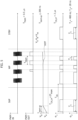
- Figure 5 is a diagram showing, with reference to a common time (abscissa) scale, possible time behaviors of signals that may occur in a receiver circuit for OOK modulation.
- Figure 5 is a diagram showing possible time behaviors of the following signals (from top to bottom):
- a period T PWM of the PWM signal equal to 0.5 microseconds can be considered in connection with a start-up time T start-up (the time for the signal V B to initially reach the signal V A ) of 200 nanoseconds.
- T 1 e.g. 400 nanoseconds
- T 2 e.g. 20 nanoseconds
- T CK,LF such that T CK,LF >2T PWM (e.g. T CK,LF equal to 2 microseconds) is also illustrated in connection with the clock signal V CK,LF as discussed in Figure 7 .
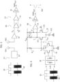
- Figure 6 is exemplary of an arrangement as presented in Figure 4 that is capable of operating adequately in (all of) the three operating phases SUP, WP and STBY presented in Figure 5 .
- circuit illustrated in Figure 6 comprises:
- the differential stage 121, 122, R L2 has first C and second D output nodes configured to produce across them a replica of the OOK signal having the RF carrier removed therefrom
- the circuit in Figure 6 comprises a comparator 16 coupled (e.g., via a gain stage 14) to the first C and second D output nodes of the differential stage 121, 122, R L2 and configured to produce, based on the replica of the OOK signal having the RF carrier removed therefrom, a PWM-modulated signal PWM OUT having on and off times.
- a comparator 16 coupled (e.g., via a gain stage 14) to the first C and second D output nodes of the differential stage 121, 122, R L2 and configured to produce, based on the replica of the OOK signal having the RF carrier removed therefrom, a PWM-modulated signal PWM OUT having on and off times.
- switches S 1 , ⁇ 1 and S 3 , ⁇ 1 are controlled via the signal ⁇ 1
- switch S 2 , ⁇ 2 is controlled via the signal ⁇ 2 .
- This kind of "dis-overlapping" advantageously counters undesired effects of the transmitted PWM signal on offset compensation, e.g., facilitating the PWM signal in being at a "low” level (switch SW turned off) during offset compensation.
- the arrangement of Figure 6 is thus exemplary of a compensation loop that exploits the first amplifier of the receiving chain (transistors M1 and M2) as an input stage and the second stage (transistors 121, 122) to increase gain.
- Such an arrangement is advantageous. e.g., with GaN technologies that have offsets (much) higher than CMOS technologies and deserve not to be neglected with respect to typical variations in the bias voltage V A .
- Figure 6 facilitates dynamic adaptative operation that uses two timing (clock) signals, one of which is synchronized to the PWM signal, with two compensation time slots.
- a possible implementation of the generator 100 (this may be either a distinct circuit or be incorporated to a single circuit with the receiver of Figure 6 ) is built around three D-type flip-flops 101, 102, and 103.
- the two first flip-flops 101, 102 are clocked via a clock signal V CK,LF (generated with a clock generator CLK of any type known to those of skill in the art, e.g., a ring oscillator: this may possible be a distinct element from the embodiments) with a period T CK,LF such that T CK,LF >2T PWM as illustrated in the diagram of Figure 5 .
- V CK,LF generated with a clock generator CLK of any type known to those of skill in the art, e.g., a ring oscillator: this may possible be a distinct element from the embodiments
- the third flip-flop 103 is clocked via the PWM signal PWM OUT from the comparator 16 (logically inverted at an inverter 104) or any other signal synchronous with such a PWM signal.
- the signal V CK,LF can be regarded as a (e.g., square wave) signal that is "slow" with respect to the PWM signal.
- the delay blocks 105 and 107 thus dictate the characteristics of the signals ⁇ 1 and ⁇ 2 (primarily the durations of the intervals T 1 and T 2 ).
- the one illustrated in Figure 7 is only one exemplary implementation of a signal generator 100 configured to provide the signals ⁇ 1 (at the output of the second NAND gate 110B) and ⁇ 2 (at the output of the first NAND gate 110A after logical inversion at the inverter 112), namely two slightly “dis-overlapped" replicas ⁇ 1 and ⁇ 2 of a same signal in order to counter undesired effects of the transmitted PWM signal on offset compensation: other implementations are within the ability of those of skill in the art.
- the one illustrated in Figure 7 is an exemplary implementation of a signal generator 100 configured provide signals ⁇ 1 and ⁇ 2 that make the first switch S 1 , ⁇ 1 , the second switch S 2 , ⁇ 2 and the third switch S 3 , ⁇ 1 conductive during the start-up phase SUP and (at least one) standby phase STBY for a time T 1 longer than the off times T 2 of the PWM-modulated signal.
- T 1 e.g. 400 nanoseconds
- T 2 e.g., 20 nanoseconds
- the logic circuitry 100 comprises:
- the circuit comprises a clock generator CLK (optionally a ring oscillator) to produce the first clock signal V CK,LF to activate the first branch 101, 102 of the logic circuitry 100 and make the switches S 1 , ⁇ 1 , S 2 , ⁇ 2 , and S 3 , ⁇ 1 , conductive (even) in the absence of the PWM-modulated signal PWM OUT .
- CLK clock generator
- V CK clock signal
- the second branch 103, 107 of the logic circuitry 100 is coupled to the comparator 16 to receive therefrom the PWM-modulated signal PWM OUT to make the switches S 1 , ⁇ 1 ; S 2 , ⁇ 2 ; and S 3 , ⁇ 1 , conductive during off times T 2 of the PWM-modulated signal.
- the logic circuitry 100 is configured to produce:
- the first signal ⁇ 1 and the second signal ⁇ 2 exhibit corresponding (i.e., substantially identical, but slightly dis-overlapped) time behaviors with the second signal ⁇ 2 having rising edges lagging the rising edges of the first signal ⁇ 1 and falling edges preceding the falling edges of the first signal ⁇ 1 .
- operation of the arrangement of Figure 6 involves, during a start-up phase SUP of the receiver, the storage capacitor C H in Figure 6 (that provides the voltage V B ) being charged from an initial value towards the voltage V A .
- the digital circuitry (e.g., essentially the generator 100, with the PWM signal not present yet) operates at low frequency clock signal (V CK,LF having a frequency f CK,LF of, e.g., 0.5 MHz) thus providing a large (long) compensation pulse T 1 .
- V CK,LF having a frequency f CK,LF of, e.g., 0.5 MHz
- the negative time slot of the PWM signal can be exploited to restore the capacitor C H and thus compensate for offset variations due to thermal drift effects.
- a narrow pulse (about 20 ns, for instance) is then generated for dynamic offset compensation (DOT in the diagram of Figure 5 ) that is suitable for the compensation even for high values for the duty cycle (e.g., 90%) when the negative time slot of the PWM signal is low (i.e., 50 ns).
- the PWM signal PWM OUT is at first "blanked" as a result of the switches S 1 , ⁇ 1 and S 3 , ⁇ 1 being still closed by the signal ⁇ 1.
- the clock signal is again switched to the low frequency clock. For instance, this may happen if the PWM signal is not present for a time higher than T CK,LF .
- a solution as proposed herein comprises offset compensation circuitry including:
- the logic circuitry 100 as exemplified in Figure 7 is configured to activate the offset compensation circuitry in a sequence of phases comprising, in the first place a start-up phase SUP where the switches S 1 , ⁇ 1 ; S 2 , ⁇ 2 , and S 3 , ⁇ 1 are made conductive in the absence of the PWM-modulated signal PWM OUT .
- the logic circuitry 100 as exemplified in Figure 7 is configured to activate a working phase WP in the presence of the PWM-modulated signal PWM OUT where the switches S 1 , ⁇ 1 ; S 2 , ⁇ 2 , S 3 , ⁇ 1 , are made conductive during off times T 2 of the PWM-modulated signal PWM OUT .
- a standby phase STBY may then follow where the switches S 1 , ⁇ 1 ; S 2 , ⁇ 2 , and S 3 , ⁇ 1 , are again made conductive in the absence of the PWM-modulated signal PWM OUT , with the circuit returning from the standby phase to working phase in response to a PWM (OOK) signal being again received via the antenna RX1. Consequently, the working phase WP can be regarded as a phase alternating with the start-up phase SUP and/or at least one standby phase STBY.
- a (further) differential stage 18 can be advantageously coupled across the first output node C and the second D output node of the differential stage 121, 122, R L2 to apply a (loop) gain to the signal indicative of the difference between the first output node C and the second output node D of the differential stage 121, 122, R L2 that is fed back to the storage capacitor C H .
- This option is found to facilitate proper operation of the compensation loop with the target of keeping at zero the difference of the voltages at the nodes C and D.
- a (further) gain stage 14 is optionally arranged between the differential stage 121, 122, R L2 and the comparator 16 with the purpose of applying a (transfer) gain to the replica of the OOK signal having the RF carrier removed that is applied to the comparator 16 to produce the PWM-modulated signal PWM OUT .
- This option is found to facilitate proper operation of the comparator in the presence of small (weak) input signals to the receiver.
- a solution as proposed herein is able to operate adequately in (all of) the three operating phases SUP, WP, and STBY illustrated in the diagram of Figure 5 . This result is facilitated by the use of two clock signals (one of which is synchronized to the transmitted signal) and two compensation time slots.
Landscapes
- Engineering & Computer Science (AREA)
- Computer Networks & Wireless Communication (AREA)
- Signal Processing (AREA)
- Power Engineering (AREA)
- Physics & Mathematics (AREA)
- Nonlinear Science (AREA)
- Amplifiers (AREA)
- Digital Transmission Methods That Use Modulated Carrier Waves (AREA)
Abstract
Description
- The description relates to signal transmission.
- Solutions as described herein can be applied, for instance, to transmission of signals between semiconductor chips or dice (oftentimes referred to as inter-chip data communication).
- Gate drivers (e.g., for electric motor control), galvanically isolated interfaces, medical equipment, sensor networks and data communications in general are exemplary of possible applications of solutions as described herein.
- Inter-chip data communication may involve transmitting a modulated radio-frequency, RF carrier between two (integrated circuit) semiconductors chips or dice: as used therein chip/chips and die/dice will be regarded as synonyms.
- This type of communication may involve transmitting a low-level RF signal that is rectified at the receiver (e.g., via an envelope detector) and then amplified to be converted into a digital (pulse-width modulated) PWM signal. A final conversion (to recover output data that replicate the transmitted data) can be performed via a hysteresis comparator.
- Offset phenomena such as, e.g., an offset voltage between the two inputs of a first amplifier in the receiver can adversely affect correct recovery of the PWM signal.
- Adequate offset compensation is thus desirable in order to facilitate accurate demodulation at the receiver.
- Document
CN 114 884 522 A discloses a differential millimeter-wave communication architecture and electronic equipment. The architecture comprises a transmitting device which comprises an oscillator, a frequency multiplier, a first differential transformer, at least one drive amplification circuit and a power amplification circuit which are connected in sequence. The driving amplification circuit comprises a driving amplifier and a second differential transformer which are connected in sequence, the power amplification circuit comprises a power amplifier and a third differential transformer which are connected in sequence, the power amplifier comprises a signal switch, and the signal switch is connected with an on-off keying signal input end. The millimeter-wave front-end circuit with low power consumption and small area can be realized. - Document
US 6 249 556 B1 discloses a method and apparatus for thresholding an input signal synchronous with a clock signal at a receiver. The input signal is compared with a threshold voltage to produce a difference signal. The difference signal is synchronized with the input signal to generate a feedback signal. The threshold voltage is adjusted based on the feedback signal. -
Document EP 1 985 011 A2 (WO 2007/088127 A2 ) discloses providing gigabit-rate data transmission over wireless radio links, using carrier frequencies in the millimeter-wave range (>30 GHz). More specifically, a circuit for detection of amplitude-shift keyed (ASK) or other amplitude modulations (AM) which can be easily incorporated into an integrated circuit receiver system is described, making the receiver capable of supporting both complex IQ modulation schemes and simpler, non-coherent on-off or multiple-level keying signals. Several radio architectures are also described which, with the addition of a frequency discriminator network, have the capability of handling frequency shift keyed (FSK) or other frequency modulations (FM), as well as AM and complex IQ modulation schemes. These radio architectures support a wide variety of modulations by efficiently sharing detector hardware components. The architecture for supporting both quadrature downconversion and ASK/AM is described first, followed by the ASK/AM detector circuit details, then the AM-FM detector architecture, and finally the most general AM-FM/IQ demodulator system concept and the FSK/FM detector circuit details. - Solutions as described herein aim at addressing the issue discussed in the foregoing.
- Such an object can be achieved via a receiver circuit having the features set forth in the claims that follow.
- One or more embodiments relate to a corresponding system. A system comprising two or more (integrated circuit) inter-communicating semiconductor chips or dice is exemplary of such system.
- One or more embodiments relate to a corresponding method.
- The claims are an integral part of the technical teaching provided in respect of the embodiments.
- Solutions as described herein provide a self-calibration technique for offset compensation in an amplitude-shift keying (ASK) receiver wherein a low-level baseband signal is amplified.
- Solutions as described herein involve a dynamic approach that facilitates dynamically compensating also an offset drift induced by a temperature change.
- Solutions as described herein do not involve external or non-standard components and are suitable for implementation via CMOS integration technology (e.g., GaN or SiC technology for power MOSFET transistors).
- Solutions as described herein provide a fully integrated solution for automatic and accurate analog self-calibration wherein manual and/or preliminary setting can be dispensed with.
- Solutions as described herein do not involve an increased power consumption and can be implemented with negligible area occupation.
- Solutions as described herein facilitate achieving package scale isolation with galvanic isolation implemented without using specific high-voltage (HV) components.
- Solutions as described herein facilitate providing an inter-chip communication channel implemented via wireless RF transmission.
- A judicious selection of the distance between two chips facilitates achieving higher isolation ratings (10-12 kV for reinforced isolation) and higher CMTI (> 100 kV): common mode transient immunity (CMTI) is defined as the maximum tolerable rate of rise or fall of a common mode voltage applied between two isolated circuits.
- This greatly facilitates arranging two inter communicating chips or dice on two neigboring die pads in a same leadframe packaged in a same body of molding compound (package scale isolation).
- Solutions as described herein employ a simple approach that can be adapted easily to different applications, offset values, and accuracy levels with a procedure that can start automatically at start-up.
- Solutions as described herein provide a self-calibration technique for offset compensation in an, e.g., ASK receiver where a low base-band signal is amplified by adopting an analog dynamic approach that facilitates compensate dynamically also offset drifts induced by temperature.
- One or more embodiments will now be described, by way of example only, with reference to the annexed figures, wherein:
-
Figure 1 is generally illustrative of communication between two circuits using a galvanic isolation barrier, -
Figure 2 is illustrative of a possible context of application of solutions as described herein, -
Figure 3 is illustrative of inter-chip data communication, -
Figure 4 is an exemplary diagram of a receiver circuit for on-off keying, OOK modulation, -
Figure 5 is a diagram showing possible time behaviors of signals that may occur in a receiver circuit for OOK modulation as described herein, -
Figure 6 is an exemplary diagram of a receiver circuit according to embodiments of the present description, and -
Figure 7 is a circuit diagram of a digital control circuit that may be used in embodiments of the present description. - Corresponding numerals and symbols in the different figures generally refer to corresponding parts unless otherwise indicated.
- The figures are drawn to clearly illustrate the relevant aspects of the embodiments and are not necessarily drawn to scale.
- The edges of features drawn in the figures do not necessarily indicate the termination of the extent of the feature.
- In the ensuing description one or more specific details are illustrated, aimed at providing an in-depth understanding of examples of embodiments of this description. The embodiments may be obtained without one or more of the specific details, or with other methods, components, materials, etc. In other cases, known structures, materials, or operations are not illustrated or described in detail so that certain aspects of embodiments will not be obscured.
- Reference to "an embodiment" or "one embodiment" in the framework of the present description is intended to indicate that a particular configuration, structure, or characteristic described in relation to the embodiment is comprised in at least one embodiment. Hence, phrases such as "in an embodiment" or "in one embodiment" that may be present in one or more points of the present description do not necessarily refer to one and the same embodiment.
- Moreover, particular conformations, structures, or characteristics may be combined in any adequate way in one or more embodiments.
- The headings/references used herein are provided merely for convenience and hence do not define the extent of protection or the scope of the embodiments.
- For simplicity and ease of explanation, throughout this description, and unless the context indicates otherwise, like parts or elements are indicated in the various figures with like reference signs, and a corresponding description will not be repeated for each and every figure.
- Also, throughout this description, a same designation may be used for brevity to designate:
- a certain node or line and a signal occurring at that node or line, and/or
- a certain component (e.g., a capacitor or a resistor) and an electrical parameter thereof (e.g., capacitance or resistance/impedance) .
-
Figure 1 is generally illustrative of communication between two circuits C1 and C2 using a galvanic isolation barrier IB (a transformer, for instance). - As illustrated, the first circuit C1 has a supply voltage VDD1 and a (first) ground GND1; the second circuit C2 has a supply voltage VDD2 and a (second) ground GND2. The voltage VDD1 may be different from the voltage VDD2 and the ground GND1 may be different from the ground GND2, with possible ground shifts.
- Communication as represented by the arrows can involve power transfer PT (e.g., from the circuit C1 to the circuit C2) and/or data transfer DT (e.g., from the circuit C1 to the circuit C2 and vice-versa).
- The circuit C1 may comprise, just by way of example, human/data interfaces, bus/network controllers, microcontroller units (MCUs).
- The circuit C2 may comprise, again just by way of example, sensor interfaces, gate drivers, intelligent power switches medical devices, a communication network.
- Again, merely by way of example, a single-channel galvanic isolated gate driver can be used across a range of switching topologies to control power switches such as silicon-carbide (SiC) or silicon MOSFET transistors and IGBT insulated-gate bipolar transistors.
-
Figure 2 is illustrative of a possible context of application of solutions as described herein, wherein the circuits C1 and C2 are (integrated circuit) semiconductor chips or dice and communication between the two chips C1 and C2 involves transmitting input data ID from the chip C1 towards the chip C2 to be recovered as output data OD. As noted, this is just a non-limiting example in so far as communication between the two chips C1 and C2 may involve transmitting data ID from the chip C2 towards the chip C1, or communication in both directions. - In the following, transmission from the chip C1 towards the chip C2 will be referred to throughout for the sake of simplicity in order to avoid making the description unduly complicated.
- Transmission as exemplified herein involves applying input data ID to a modulator (e.g., a pulse-width modulator) PWMM to produce a PWM-modulated signal that is applied to a transmitter TX for transmission via transmitter (micro)antenna TX1.
- The transmitted signal is received via a receiver RX coupled to a receiver (micro) antenna RX1 to and transferred as a pulse-width modulated (PWM) signal to a demodulator (e.g., a pulse-width demodulator) PWMD to produce output data OD.
- In certain applications as discussed in the following (these may be in the automotive sector, for instance) such an output PWM signal PWMOUT can be used to drive an electronic switch such as, e.g., a power MOSFET transistor.
- Various approaches (a transformer approach, a capacitive approach, an opto-coupler approach) can be resorted to in order to implement an arrangement as exemplified in
Figure 2 . - Solutions as described herein can be advantageously incorporated to the receiver RX as discussed in the following. To that effect, reinforced galvanic isolation interfaces (e.g., 10 kV) not bound to a specific integration technology is desirable.
-
Figure 3 further illustrates inter-chip data communication under the, non-limiting, assumption that the input signal ID is a baseband binary signal that on-off modulates a radio-frequency carrier signal RF. - As illustrated in
Figure 3 , the receiver RX comprises anenvelope detector 10 coupled to the receiver antenna RX1. -
Figure 4 shows anenvelope detector 10 implemented via two MOSFET transistors M1, M2 having their control terminals (gates, in the case of field-effect transistors such as MOSFETs) coupled to the galvanic barrier IB (e.g., across the secondary winding of a transformer providing the galvanic barrier IB) and the current flow paths therethrough (source-drain, in the case of a field-effect transistors such as MOSFETs) arranged in parallel in a current flow line between a supply line at a voltage VDD and ground GND. - In certain embodiments, the flow of common-mode transient immunity (CMTI) currents towards ground can be facilitated by coupling the receiver RX in an AC (alternate current) mode to the antenna RX1 via two decoupling capacitances while a central socket of the antenna is connected to ground.
- As illustrated in
Figure 4 , a resistor RL1 is arranged between the supply line VDD and the parallel connection of the current flow paths through the MOSFET transistors M1, M2 with a (envelope) voltage VA available at a corresponding node between the resistor RL1 and the MOSFET transistors M1, M2. Advantageously, a capacitor CED (shown in dashed lines) is coupled between the node VA and ground (or between the node VA and the line VDD) to remove residues of the RF carrier from the signal obtained from theenvelope detector 10. - The one exemplified here (this also applies to the discussion of
Figure 6 that follows) otherwise represents just one of a plurality of possible implementations of an envelope detector known to those of skill in the art that may resorted to within the framework of a solution as discussed herein. - Turning back to the more general representation of
Figure 3 , the envelope detector 10 (however implemented) is coupled to a first input (node VA) of adifferential amplifier 12 having a second input at a value VB. - As illustrated, the output from the
differential amplifier 12 is coupled (e.g., via afurther amplifier 14 providing additional gain) to a (hysteresis)comparator 16 whose output is a PWM-modulated signal PWMOUT suited to drive a load, e.g., to on-off turn an electronic switch SW such as a power MOSFET transistor. - It is noted that the load (e.g., the switch SW) is usually a distinct element from the embodiments.
- In inter-chip data communication as illustrated in
Figure 3 two micro-antennas TX1, RX1 are used to transmit a modulated RF carrier between two chips C1 and C2. - The low-level RF signal at the receiver is thus rectified (at the envelope detector 10) and then amplified (at the gain stages 12 and 14) to be applied to a
hysteresis comparator 16 to provide an output PWM signal PWMOUT. - An offset voltage between the two nodes VA, VB (the inputs to the amplifier 12) can adversely affect an even compromise a correct recovery of the PWM signal. Applying an offset compensation technique to compensate that offset voltage thus facilitates accurate demodulation of the PWM signal.
- A related offset compensation circuit should desirably operate not only at start-up and standby conditions but also during operation in so far as this facilitates compensating offset drift effects.
-
Figure 4 , already partly discussed, illustrates an exemplary diagram of a receiver circuit for on-off keying, OOK modulation, where the galvanic barrier IB is illustrated implemented as a transformer, and theenvelope detector 10 is implemented via two MOSFET transistors M1, M2 having their control terminals (gates, in the case of field-effect transistors such as MOSFETs) coupled to the galvanic barrier IB (across the secondary winding of the transformer) and the current flow paths therethrough (source-drain, in the case of a field-effect transistors such as MOSFETs) arranged in parallel in a current flow line between a supply line at a voltage VDD and ground GND. - As noted, a resistor RL1 is arranged between the supply line VDD and the parallel connection of the current flow paths through the MOSFET transistors M1, M2, with the capacitor CED (shown in dashed lines) coupled between the node VA and ground (or the line VDD) to remove residues of the RF carrier from the signal from the
envelope detector 10. - The envelope signal VA between the resistor RL1 and the MOSFET transistors M1, M2 is applied to the input of the
first amplifier stage 12 that comprises a differential pair of two (e.g., MOSFET)transistors - A tail
current generator 123 is provided between thetransistors transistors - Two resistors (both referenced as RL2) are arranged coupled each between the supply line VDD and:
- a node C at the current flow path through the
transistor 121, and - a node D at the current flow path through the
transistor 122. - The output from the
amplifier stage 12 is obtained as a differential signal between the nodes C and D and applied to the (differential)gain stage 14 to be then delivered to the input of thehysteresis comparator 16 that produces the output signal PWMOUT the original PWM signal. - Various approaches can be considered for countering undesired offsets in a receiver as discussed previously.
- A first approach may involve manual trimming using metal or "poly" fuses (eFuses). For instance, such fuses can replace the switches in the resistive string RL2 in
Figure 4 . Such an approach inevitably results in increase of the cost of in production testing. Also, high currents may be involved in blowing the fuse. - Another approach may involve using a floating gate MOSFET transistor to implement an analog trim-voltage memory (ATVM). Such an ATVM can be used for trimming offset voltages and currents resulting from threshold mismatches in analog circuits such as operational amplifiers and comparators. It can be incorporated into a standard digital CMOS process without additional processing steps as those currently involved in EEPROM fabrication. However, it still involves the non-negligible provision of additional elements.
- Still another approach may involve using a one-time programmable (OTP) non-volatile memory (NVM) such an e-fuse or antifuse to replace floating-gate or e-fuse techniques as sued in analog/sensor trimming and calibration. Macros of the OTP type offer a good deal of security, reliability and flexibility as desirable to cost-effectively implement analog trimming and calibrate operations in consumer, automotive and mobile communication devices (ADC, receivers etc.). Also, die area occupation of an OTP element is small, and this reduces cost.
- A drawback of this approach lies in the need for an initial programming phase either after chip packaging or by the user.
- A still further approach may involve digital offset cancellation in a self-calibration technique: this approach is not able to support satisfactorily various operation phases such as start-up, working (operation proper) and standby as desirable for gate drivers. Applications with higher PWM rates (e.g., PWM rates higher than 400 KHz) are not compatible with PWM data transmission.
- In solution as described herein an offset compensation solution is proposed based on a mixed analog/digital offset compensation strategy that is capable of tracking process, voltage and temperature (PVT) variations during different operating conditions, e.g., start-up, working, and standby conditions.
-
Figure 5 is a diagram showing, with reference to a common time (abscissa) scale, possible time behaviors of signals that may occur in a receiver circuit for OOK modulation. - More specifically,
Figure 5 is a diagram showing possible time behaviors of the following signals (from top to bottom): - a PWM input signal PWM IN (modulated onto a RF carrier);
- a corresponding PWM output signal PWMOUT;
- a possible offset signal VOS = VA - VB between the nodes VA and VB; and
- two compensation control signals Φ1 and Φ2 produced as discussed in the following.
- Specifically, possible time behaviors of the signals identified above are shown (from left to right) with reference to three different phases:
- a start-up phase SUP, without any PWM signal assumed to be applied to the receiver;
- a working phase WP, with a PWM (e.g., data) signal assumed to be applied to the receiver;
- a stand-by phase STBY, again without any PWM signal assumed to be applied.
- Merely by way of example (and without limitations for the embodiments) a period TPWM of the PWM signal equal to 0.5 microseconds can be considered in connection with a start-up time Tstart-up (the time for the signal VB to initially reach the signal VA) of 200 nanoseconds.
- A dynamic offset compensation DOT (of a duration of about 20 nanoseconds) is shown in the curve for the possible offset signal VOS = VA - VB.
- The times T1 (e.g., 400 nanoseconds) and T2 (e.g., 20 nanoseconds) are shown in the two lowermost curves of
Figure 5 for the two signals Φ1 and Φ2. - A time TCK,LF such that TCK,LF>2TPWM (e.g. TCK,LF equal to 2 microseconds) is also illustrated in connection with the clock signal VCK,LF as discussed in
Figure 7 . - All of the quantitative figures referred to in the foregoing are merely exemplary and non-limiting: they are given primarily with the aim of elucidating certain relationships that may exist between the durations of various signals discussed herein.
-
Figure 6 is exemplary of an arrangement as presented inFigure 4 that is capable of operating adequately in (all of) the three operating phases SUP, WP and STBY presented inFigure 5 . - In
Figure 6 , parts or elements like parts or elements already discussed in connection withFigure 4 are indicated with like reference numbers/symbols and a corresponding detailed description will not be repeated for brevity. - Also, like parts or elements being indicated with like reference numbers/symbols in
Figure 4 andFigure 6 does not imply that these parts or elements need be implemented in the same manner in in both cases. - To summarize, the circuit illustrated in
Figure 6 comprises: - an envelope detector M1, M2, RL1, CED configured to receive (via the antenna RX1) an on-off keying, OOK signal modulated over a radiofrequency, RF carrier and remove therefrom the RF carrier,
- a
differential stage - As illustrated, the
differential stage - As illustrated, the circuit in
Figure 6 comprises acomparator 16 coupled (e.g., via a gain stage 14) to the first C and second D output nodes of thedifferential stage - Comparing the circuit diagram of
Figure 6 with the circuit diagram ofFigure 4 shows that, in the circuit diagram ofFigure 6 : - a capacitor CH is coupled between the node VB (control terminal of the transistor 122) and ground GND;
- a
differential amplifier 18 is optionally coupled with its inputs (inverting, "-" and non-inverting, "+") coupled to the nodes C and D to provide additional (loop) gain to the difference between the voltages at these nodes (offset compensation as discussed in the following involves feeding this difference back to the node VB targeting a zero value). - Comparing the circuit diagram of
Figure 6 with the circuit diagram ofFigure 4 also shows that, in the circuit diagram ofFigure 6 three switches S1,Φ1, S2,Φ2 and S3,Φ1 (e.g., electronic switches such as MOSFET transistors) are provided configured, when "on" (that is when made conductive): - to short-circuit the output from the isolation barrier, namely the input to the envelope detector 10 (transistors M1, M2) of the receiver (switch S1,Φ1 - driven via the signal Φ1);
- to couple the node VB (that is the capacitor CH) to the output from the
amplifier 18 to apply there to a signal indicative of the difference between the voltages at the nodes C and D (switch S2,Φ2 - driven via the signal Φ2); and - to short towards ground GND the line coupling the
amplifier 14 and the hysteresis comparator 16 (switch S3,Φ1 - driven via the signal Φ1), - Operation (on-off switching) the switches S1,Φ1, S2,Φ2 and S3,Φ1 is controlled via the signals Φ1 and Φ2. These signals can be produced via a
signal generator 100 as illustrated in the diagram ofFigure 7 . - It is noted that the switches S1,Φ1 and S3,Φ1 are controlled via the signal Φ1, while the switch S2,Φ2 is controlled via the signal Φ2.
- It is otherwise noted that (as visible in the two lowermost curves in the diagram of
Figure 5 ) the signals Φ1 and Φ2 have corresponding time behaviors (that is, essentially the same time behavior) with the exception that the signal Φ2 has: - rising edges (slightly) lagging (i.e., following) the rising edges of the signal Φ1, and
- falling edges (slightly) preceding (i.e., anticipating) the falling edges of the signal Φ1.
- This kind of "dis-overlapping" advantageously counters undesired effects of the transmitted PWM signal on offset compensation, e.g., facilitating the PWM signal in being at a "low" level (switch SW turned off) during offset compensation.
- Undesired inaccuracies in offset compensation during the start-up (SUP) and standby (STBY) phases are countered in so far the receiver input is short-circuited by the switch S1,Φ1 and the input to the
comparator 16 is forced to zero (GND) by the switch S3,Φ1 so that no PWM signal (and also no input noise) propagates through the receiver. Also, offset compensation during the working phase (WP), when a PWM signal is expected to propagate through the receiver, is effected during the "off" times of the PWM signal, that is when the PWM signal is at zero level. - The arrangement of
Figure 6 is thus exemplary of a compensation loop that exploits the first amplifier of the receiving chain (transistors M1 and M2) as an input stage and the second stage (transistors 121, 122) to increase gain. - Such an arrangement is advantageous. e.g., with GaN technologies that have offsets (much) higher than CMOS technologies and deserve not to be neglected with respect to typical variations in the bias voltage VA.
- Advantageously, the arrangement of
Figure 6 (andFigure 7 ) facilitates dynamic adaptative operation that uses two timing (clock) signals, one of which is synchronized to the PWM signal, with two compensation time slots. - As illustrated herein, this result is facilitated by a mixed analog/digital compensation approach, which combines analog compensation and digital control.
- A possible implementation of the generator 100 (this may be either a distinct circuit or be incorporated to a single circuit with the receiver of
Figure 6 ) is built around three D-type flip-flops - The two first flip-
flops Figure 5 . - The third flip-
flop 103 is clocked via the PWM signal PWMOUT from the comparator 16 (logically inverted at an inverter 104) or any other signal synchronous with such a PWM signal. Essentially, as discussed in the following, the signal VCK,LF can be regarded as a (e.g., square wave) signal that is "slow" with respect to the PWM signal. - As illustrated in
Figure 7 : - the first flip-
flop 101 is arranged with its (negated) Q output coupled to its D input and the Q output coupled to the D input to the second flip-flop 102; - the Q output from the second flip-
flop 102 is fed back via a (first)delay block 105 to the reset input R of the second flip-flop 102 and to a first input of a (first) ORgate 106 that drives the reset input R of the first flip-flop 101; - the third flip-
flop 103 is arranged with its D input set to the supply voltage VDD and the Q output fed back via a (second)delay block 107 to the reset input R of the third flip-flop 103 and to the other input of theOR gate 106 that drives the reset input R of the first flip-flop 101; - the Q outputs of the second and third flip-
flops gate 108, whose output drives a pair ofNAND gates - the
first NAND gate 110A receives, on a first input, the output of theOR gate 108 and, on a second input, the output of the second ofNAND gate 110B; and - the
second NAND gate 110B receives, on a first input, the output of theOR gate 108 logically inverted at aninverter 111 and, on a second input, the output of thefirst NAND gate 110A (as obtained via two complementary logical inversions at twoinverters - The delay blocks 105 and 107 thus dictate the characteristics of the signals Φ1 and Φ2 (primarily the durations of the intervals T1 and T2).
- As noted, the one illustrated in
Figure 7 is only one exemplary implementation of asignal generator 100 configured to provide the signals Φ1 (at the output of thesecond NAND gate 110B) and Φ2 (at the output of thefirst NAND gate 110A after logical inversion at the inverter 112), namely two slightly "dis-overlapped" replicas Φ1 and Φ2 of a same signal in order to counter undesired effects of the transmitted PWM signal on offset compensation: other implementations are within the ability of those of skill in the art. - To summarize, the one illustrated in
Figure 7 is an exemplary implementation of asignal generator 100 configured provide signals Φ1 and Φ2 that make the first switch S1,Φ1, the second switch S2,Φ2 and the third switch S3,Φ1 conductive during the start-up phase SUP and (at least one) standby phase STBY for a time T1 longer than the off times T2 of the PWM-modulated signal. - In the examples considered herein the PWM-modulated signal PWMOUT has a period (e.g., TPWM = 0.5 microseconds) and the
logic circuitry 100 is configured to make the first switch S1,Φ1, the second switch S2,Φ2 and the third switch S3,Φ1 conductive during the start-up and standby phases for a time T1 (e.g., 400 nanoseconds) that is at least one order of magnitude (that, is at least ten times) longer than the off times T2 (e.g., 20 nanoseconds) of the PWM-modulated signal. - As exemplified in
Figure 7 , thelogic circuitry 100 comprises: - a first branch (e.g., the
integers - a second branch (e.g., the
integers 103, 107) configured to be activated during the working phase WP to make the switches S1,Φ1; S2,Φ2, and S3,Φ1 conductive during off times T2 of the PWM-modulated signal. - As illustrated, the circuit comprises a clock generator CLK (optionally a ring oscillator) to produce the first clock signal VCK,LF to activate the
first branch logic circuitry 100 and make the switches S1,Φ1, S2,Φ2, and S3,Φ1, conductive (even) in the absence of the PWM-modulated signal PWMOUT. - As illustrated, the
second branch logic circuitry 100 is coupled to thecomparator 16 to receive therefrom the PWM-modulated signal PWMOUT to make the switches S1,Φ1; S2,Φ2; and S3,Φ1, conductive during off times T2 of the PWM-modulated signal. - As illustrated, the
logic circuitry 100 is configured to produce: - a first drive signal Φ1 to make the first switch S1,Φ1 and the third switch S3,Φ1, conductive, and
- a second drive signal Φ2 to make the second switch S2,Φ2 conductive.
- As illustrated, the first signal Φ1 and the second signal Φ2 exhibit corresponding (i.e., substantially identical, but slightly dis-overlapped) time behaviors with the second signal Φ2 having rising edges lagging the rising edges of the first signal Φ1 and falling edges preceding the falling edges of the first signal Φ1.
- As exemplified in the diagram of
Figure 5 , operation of the arrangement ofFigure 6 (andFigure 7 ) involves, during a start-up phase SUP of the receiver, the storage capacitor CH inFigure 6 (that provides the voltage VB) being charged from an initial value towards the voltage VA. - As visible on the left-hand side of the diagram for the voltage VB in
Figure 5 this process takes place "slowly" (due to slewing limitations) during a first charging pulse of duration T1 that represents the compensation time slot during the start-up phase SUP (and also in stand-by conditions STBY, as discussed in the following). - To that purpose, the digital circuitry (e.g., essentially the
generator 100, with the PWM signal not present yet) operates at low frequency clock signal (VCK,LF having a frequency fCK,LF of, e.g., 0.5 MHz) thus providing a large (long) compensation pulse T1. - During the working phase WP (center portion of
Figure 5 ), with the PWM signal present, the negative time slot of the PWM signal can be exploited to restore the capacitor CH and thus compensate for offset variations due to thermal drift effects. - During the working phase WP, the clock of the digital circuit is switched from the previous low-frequency clock to a clock that is extracted from the PWM signal (e.g., with a frequency fPWM = 2 MHz). A narrow pulse (about 20 ns, for instance) is then generated for dynamic offset compensation (DOT in the diagram of
Figure 5 ) that is suitable for the compensation even for high values for the duty cycle (e.g., 90%) when the negative time slot of the PWM signal is low (i.e., 50 ns). - It is noted that, during the working phase WP as represented in
Figure 5 , the PWM signal PWMOUT is at first "blanked" as a result of the switches S1,Φ1 and S3,Φ1 being still closed by the signal Φ1. - It is noted that the highest number of PWM pulses that can be lost during compensation in the start-up and/or standby phases (SUP and STBY, respectively) due to offset compensation is equal to fPWM/2fCK,LF (e.g., 2 in the exemplary implementation presented herein).
- During the standby phase STBY (right-hand portion of
Figure 5 ), where the PWM signal is no longer transmitted, the clock signal is again switched to the low frequency clock. For instance, this may happen if the PWM signal is not present for a time higher than TCK,LF. - It will be appreciated that, while a sequence of a start-up phase SUP, a working phase WP and standby phase STBY is illustrated in
Figure 5 , operation of a receiver as discussed herein may involve, after a start-up phase SUP, an alternation of working phases WP and standby phases STBY depending on whether a PWM signal is transmitted or not. - It is once more noted that the highest number of PWM pulses that can be lost as a result of compensation during in the start-up and/or standby phases (SUP and STBY, respectively) - see the left-hand side of the central portion in
Figure 5 , where the PWM signal is initially blanked - is equal to fPWM/2fCK,LF (e.g., 2 in the exemplary implementation presented herein. - To summarize, a solution as proposed herein comprises offset compensation circuitry including:
- a first switch S1,Φ1 operable to be made conductive to short-circuit the input to the envelope detector M1, M2, RL1, CED,
- a storage capacitor CH coupled to the second input VB of the
differential stage - a second switch S2,Φ2 operable to be made conductive to feed back to the storage capacitor CH a signal (e.g., from the differential stage 18) indicative of the difference between the first output node C and the second D output node of the
differential stage - a third switch S3,Φ1, operable to be made conductive to short-circuit the input to the
comparator 16. - The
logic circuitry 100 as exemplified inFigure 7 is configured to activate the offset compensation circuitry in a sequence of phases comprising, in the first place a start-up phase SUP where the switches S1,Φ1; S2,Φ2, and S3,Φ1 are made conductive in the absence of the PWM-modulated signal PWMOUT. - Once the start-up phase completed, the
logic circuitry 100 as exemplified inFigure 7 is configured to activate a working phase WP in the presence of the PWM-modulated signal PWMOUT where the switches S1,Φ1; S2,Φ2, S3,Φ1, are made conductive during off times T2 of the PWM-modulated signal PWMOUT. - A standby phase STBY may then follow where the switches S1,Φ1; S2,Φ2, and S3,Φ1, are again made conductive in the absence of the PWM-modulated signal PWMOUT, with the circuit returning from the standby phase to working phase in response to a PWM (OOK) signal being again received via the antenna RX1. Consequently, the working phase WP can be regarded as a phase alternating with the start-up phase SUP and/or at least one standby phase STBY.
- As discussed, a (further)
differential stage 18 can be advantageously coupled across the first output node C and the second D output node of thedifferential stage differential stage - As discussed, a (further)
gain stage 14 is optionally arranged between thedifferential stage comparator 16 with the purpose of applying a (transfer) gain to the replica of the OOK signal having the RF carrier removed that is applied to thecomparator 16 to produce the PWM-modulated signal PWMOUT. - This option is found to facilitate proper operation of the comparator in the presence of small (weak) input signals to the receiver.
- A solution as proposed herein is able to operate adequately in (all of) the three operating phases SUP, WP, and STBY illustrated in the diagram of
Figure 5 . This result is facilitated by the use of two clock signals (one of which is synchronized to the transmitted signal) and two compensation time slots. - Without prejudice to the underlying principles, the details and embodiments may vary, even significantly, with respect to what has been described by way of example only without departing from the extent of protection. The extent of protection is determined by the annexed claims.
Claims (10)
- A circuit, comprising:an envelope detector (M1, M2, RL1, CED) configured to receive (RX1) an on-off keying, OOK signal modulated over a radiofrequency, RF carrier and remove therefrom the RF carrier,a differential stage (121, 122, RL2) having a first input (VA) coupled to the envelope detector (M1, M2, RL1, CED) and a second input (VB) configured to receive a reference signal, the differential stage (121, 122, RL2) having first (C) and second (D) output nodes configured to produce therebetween a replica of the OOK signal having the RF carrier removed therefrom, anda comparator (16) coupled (14) to the first (C) and second (D) output nodes of the differential stage (121, 122, RL2) and configured to produce, based on said replica of the OOK signal having the RF carrier removed therefrom, a PWM-modulated signal (PWMOUT) having on and off times,wherein the circuit comprises:offset compensation circuitry including a first switch (S1,Φ1) operable to be made conductive to short-circuit the input to the envelope detector (M1, M2, RL1, CED), a storage capacitor (CH) coupled to the second input (VB) of the differential stage (121, 122, RL2) as well as a second switch (S1,Φ2) operable to be made conductive to feed back to the storage capacitor (CH) a signal (18) indicative of the difference between the first output node (C) and the second (D) output node of the differential stage (121, 122, RL2), and a third switch (S3,Φ1) operable to be made conductive to short-circuit the input to the comparator (16), andlogic circuitry (100) configured to activate the offset compensation circuitry in a sequence of phases comprising:a start-up phase (SUP) and at least one standby phase (STBY) wherein the first switch (S1,Φ1), the second switch (S2,Φ2) and the third switch (S3,Φ1) are made conductive in the absence of the PWM-modulated signal (PWMOUT), anda working phase (WP) alternating with the start-up phase (SUP) or the at least one standby phase (STBY) in the presence of the PWM-modulated signal (PWMOUT) wherein the first switch (S1,Φ1), the second switch (S2,Φ2) and the third switch (S3,Φ1) are made conductive during off times (T2) of the PWM-modulated signal (PWMOUT),wherein the circuit comprises a gain stage (14) arranged between the differential stage (121, 122, RL2) and the comparator (16) configured to apply a transfer gain to said replica of the OOK signal having the RF carrier removed therefrom applied to the comparator to produce the PWM-modulated signal (PWMOUT) having on- and off-times.
- The circuit of claim 1, wherein the logic circuitry (100) is configured to make the first switch (S1,Φ1), the second switch (S2,Φ2) and the third switch (S3,Φ1) conductive during the start-up phase (SUP) and the at least one standby phase (STBY) for a time (T1) longer than the off times (T2) of the PWM-modulated signal.
- The circuit of claim 2, wherein the PWM-modulated signal (PWMOUT) has a period (TPWM) and the logic circuitry (100) is configured to make the first switch (S1,Φ1), the second switch (S2,Φ2) and the third switch (S3,Φ1) conductive during the start-up phase (SUP) and the at least one standby phase (STBY) for a time (T1) at least one order of magnitude longer than the off times (T2) of the PWM-modulated signal.
- The circuit of any of the previous claims, wherein the logic circuitry (100) comprises:a first branch (101, 102, 105) configured to be activated during the start-up phase (SUP) and the at least one standby phase (STBY) to make the first switch (S1,Φ1), the second switch (S2,Φ2) and the third switch (S3,Φ1) conductive in the absence of the PWM-modulated signal (PWMOUT) as a function of a first clock signal (VCK,LF), anda second branch (103, 107) configured to be activated during the working phase (WP) to make the first switch (S1,Φ1), the second switch (S2,Φ2) and the third switch (S3,Φ1) conductive during off times (T2) of the PWM-modulated signal.
- The circuit of claim 4, wherein:the circuit comprises a clock generator (CLK), preferably a ring oscillator, configured to produce the first clock signal (VCK,LF) to activate the first branch (101, 102) of the logic circuitry (100) to make the first switch (S1,Φ1), the second switch (S2,Φ2) and the third switch (S3,Φ1) conductive in the absence of the PWM-modulated signal (PWMOUT) and/orthe second branch (103, 107) of the logic circuitry (100) is coupled to said comparator (16) to receive therefrom said PWM-modulated signal (PWMOUT) to make the first switch (S1,Φ1), the second switch (S2,Φ2) and the third switch (S3,Φ1) conductive during off times (T2) of the PWM-modulated signal.
- The circuit of any of the previous claims, wherein:the logic circuitry (100) is configured to produce a first drive signal (Φ1) to make the first switch (S1,Φ1) and the third switch (S3,Φ1) conductive and a second drive signal (Φ2) to make the second switch S2,Φ2) conductive, andthe first signal (Φ1) and the second signal (Φ2) have corresponding time behaviors with the second signal (Φ2) having rising edges lagging the rising edges of the first signal (Φ1) and falling edges preceding the falling edges of the first signal (Φ1) .
- The circuit of any of the previous claims, comprising:
a further differential stage (18) coupled to the first output node (C) and the second (D) output node of the differential stage (121, 122, RL2) and configured to apply a loop gain to the signal indicative of the difference between the first output node (C) and the second (D) output node of the differential stage (121, 122, RL2) fed back to the storage capacitor (CH) in response to the second switch (S2,Φ2) being made conductive. - The circuit of any of the previous claims, comprising an electronic switch (SW), preferably a power transistor, coupled to said comparator (16) and configured to be driven as a function of said PWM-modulated signal (PWMOUT) .
- A system comprising:
a plurality of semiconductor chips (C1, C2) configured to communicate via an on-off keying, OOK signal modulated over a radiofrequency, RF carrier, wherein at least one (C2) of the chips in the plurality comprises a circuit (RX) according to any of the preceding claims with said envelope detector (M1, M2, RL1, CED) configured to receive (RX1) said OOK signal. - A method, comprising:receiving an on-off keying, OOK signal modulated over a radiofrequency, RF carrier at an envelope detector (M1, M2, RL1, CED) to remove the RF carrier from said OOK signal,producing a replica of the OOK signal having the RF carrier removed therefrom between first (C) and second (D) output nodes of a differential stage (121, 122, RL2) having a first input (VA) coupled to the envelope detector (M1, M2, RL1, CED) and a second input (VB) configured to receive a reference signal, andproducing, via a comparator (16) coupled (14) to the first (C) and second (D) output nodes of the differential stage (121, 122, RL2), a PWM-modulated signal (PWMOUT) having on and off times based on said replica of the OOK signal having the RF carrier removed therefrom,wherein the method further comprises:providing a first switch (S1,Φ1) operable to be made conductive to short-circuit the input to the envelope detector (M1, M2, RL1, CED), a storage capacitor (CH) coupled to the second input (VB) of the differential stage (121, 122, RL2) as well as a second switch (S1,Φ2) operable to be made conductive to feed back to the storage capacitor (CH) a signal (18) indicative of the difference between the first output node (C) and the second (D) output node of the differential stage (121, 122, RL2), and a third switch (S3,Φ1) operable to be made conductive to short-circuit the input to the comparator (16), andactivate a sequence of offset compensation phases comprising:a start-up phase (SUP) and at least one standby phase (STBY) making the first switch (S1,Φ1), the second switch (S2,Φ2) and the third switch (S3,Φ1) conductive in the absence of the PWM-modulated signal (PWMOUT), anda working phase (WP) alternating with the start-up phase (SUP) or the at least one standby phase (STBY) in the presence of the PWM-modulated signal (PWMOUT) making the first switch (S1,Φ1), the second switch (S2,Φ2) and the third switch (S3,Φ1) conductive during off times (T2) of the PWM-modulated signal (PWMOUT),wherein the method comprises applying via a gain stage (14) arranged between the differential stage (121, 122, RL2) and the comparator (16) a transfer gain to said replica of the OOK signal having the RF carrier removed therefrom applied to the comparator to produce the PWM-modulated signal (PWMOUT) having on- and off-times.
Applications Claiming Priority (1)
| Application Number | Priority Date | Filing Date | Title |
|---|---|---|---|
| IT102023000000495A IT202300000495A1 (en) | 2023-01-16 | 2023-01-16 | RECEIVER CIRCUIT, CORRESPONDING SYSTEM AND PROCEDURE |
Publications (1)
| Publication Number | Publication Date |
|---|---|
| EP4401323A1 true EP4401323A1 (en) | 2024-07-17 |
Family
ID=85685778
Family Applications (1)
| Application Number | Title | Priority Date | Filing Date |
|---|---|---|---|
| EP23219526.3A Pending EP4401323A1 (en) | 2023-01-16 | 2023-12-21 | Receiver circuit, corresponding system and method |
Country Status (3)
| Country | Link |
|---|---|
| US (1) | US20240243698A1 (en) |
| EP (1) | EP4401323A1 (en) |
| IT (1) | IT202300000495A1 (en) |
Families Citing this family (1)
| Publication number | Priority date | Publication date | Assignee | Title |
|---|---|---|---|---|
| IT202300005733A1 (en) | 2023-03-27 | 2024-09-27 | St Microelectronics Int Nv | CORRESPONDING COMMUNICATION CIRCUIT, SYSTEM AND PROCEDURE |
Citations (3)
| Publication number | Priority date | Publication date | Assignee | Title |
|---|---|---|---|---|
| US6249556B1 (en) | 1998-05-27 | 2001-06-19 | Intel Corporation | Dynamic thresholding for input receivers |
| WO2007088127A2 (en) | 2006-01-31 | 2007-08-09 | International Business Machines Corporation | Receiver and integrated am-fm/iq demodulators for gigabit-rate data detection |
| CN114884522A (en) | 2022-04-21 | 2022-08-09 | 德氪微电子(深圳)有限公司 | Differential millimeter wave communication architecture and electronic equipment |
-
2023
- 2023-01-16 IT IT102023000000495A patent/IT202300000495A1/en unknown
- 2023-12-21 EP EP23219526.3A patent/EP4401323A1/en active Pending
-
2024
- 2024-01-10 US US18/409,527 patent/US20240243698A1/en active Pending
Patent Citations (4)
| Publication number | Priority date | Publication date | Assignee | Title |
|---|---|---|---|---|
| US6249556B1 (en) | 1998-05-27 | 2001-06-19 | Intel Corporation | Dynamic thresholding for input receivers |
| WO2007088127A2 (en) | 2006-01-31 | 2007-08-09 | International Business Machines Corporation | Receiver and integrated am-fm/iq demodulators for gigabit-rate data detection |
| EP1985011A2 (en) | 2006-01-31 | 2008-10-29 | International Business Machines Corporation | Receiver and integrated am-fm/iq demodulators for gigabit-rate data detection |
| CN114884522A (en) | 2022-04-21 | 2022-08-09 | 德氪微电子(深圳)有限公司 | Differential millimeter wave communication architecture and electronic equipment |
Also Published As
| Publication number | Publication date |
|---|---|
| US20240243698A1 (en) | 2024-07-18 |
| IT202300000495A1 (en) | 2024-07-16 |
Similar Documents
| Publication | Publication Date | Title |
|---|---|---|
| US12218576B2 (en) | Interface for passing control information over an isolation channel | |
| USRE44415E1 (en) | Wireless communication medium and method for operating the same | |
| JP5259958B2 (en) | RF backscatter transmission with zero DC power consumption | |
| US11888658B2 (en) | Transmitter for dual communication over an isolation channel | |
| US12034577B2 (en) | Demodulator for an isolation communication channel for dual communication | |
| EP3591432A1 (en) | Communication unit, integrated circuit and method for clock distribution and synchronization | |
| US20240243698A1 (en) | Receiver circuit, corresponding system and method | |
| US12095423B2 (en) | Envelope detector circuit, corresponding receiver circuit and galvanic isolator device | |
| CN114268142A (en) | Dynamic fast charge pulse generator for RF circuits | |
| US12132495B2 (en) | Telepowered contactless card | |
| US20020145469A1 (en) | Signal transmitter with pulse-controlled amplification | |
| WO2018044755A1 (en) | Fuse state sensing circuits, devices and methods | |
| CN221929843U (en) | Receiver circuit and system including receiver circuit | |
| US11750234B2 (en) | Digital self-calibration for automatic offset cancellation | |
| CN115149907B (en) | Envelope detector circuit, corresponding receiver circuit and current isolator device | |
| US20260113035A1 (en) | Monolithically-integrated circuit, system, electronic device and method | |
| US9991917B2 (en) | Demodulator, receiver and method of data communications | |
| US6717427B2 (en) | Circuit arrangement | |
| CN221103319U (en) | Signal delay setting circuit, isolated integrated circuit and power conversion circuit system | |
| TWI916423B (en) | Transmitter for dual communication over an isolation channel | |
| US11601125B2 (en) | Switch control device | |
| EP4412090A1 (en) | Sample and hold circuit and method for analog-to-digital conversion | |
| CN119892039A (en) | Signal delay setting circuit, isolated integrated circuit and power conversion circuit system | |
| US9641362B2 (en) | N-wire two-level digital interface | |
| JPH02202745A (en) | Communication system |
Legal Events
| Date | Code | Title | Description |
|---|---|---|---|
| PUAI | Public reference made under article 153(3) epc to a published international application that has entered the european phase |
Free format text: ORIGINAL CODE: 0009012 |
|
| STAA | Information on the status of an ep patent application or granted ep patent |
Free format text: STATUS: THE APPLICATION HAS BEEN PUBLISHED |
|
| AK | Designated contracting states |
Kind code of ref document: A1 Designated state(s): AL AT BE BG CH CY CZ DE DK EE ES FI FR GB GR HR HU IE IS IT LI LT LU LV MC ME MK MT NL NO PL PT RO RS SE SI SK SM TR |
|
| STAA | Information on the status of an ep patent application or granted ep patent |
Free format text: STATUS: REQUEST FOR EXAMINATION WAS MADE |
|
| 17P | Request for examination filed |
Effective date: 20240924 |
|
| RBV | Designated contracting states (corrected) |
Designated state(s): AL AT BE BG CH CY CZ DE DK EE ES FI FR GB GR HR HU IE IS IT LI LT LU LV MC ME MK MT NL NO PL PT RO RS SE SI SK SM TR |