EP4401307A1 - Methods and techniques to achieve target phase shift over wide frequency band in the input of doherty power amplifiers - Google Patents
Methods and techniques to achieve target phase shift over wide frequency band in the input of doherty power amplifiers Download PDFInfo
- Publication number
- EP4401307A1 EP4401307A1 EP24150768.0A EP24150768A EP4401307A1 EP 4401307 A1 EP4401307 A1 EP 4401307A1 EP 24150768 A EP24150768 A EP 24150768A EP 4401307 A1 EP4401307 A1 EP 4401307A1
- Authority
- EP
- European Patent Office
- Prior art keywords
- amplifier
- input
- phase
- doherty
- terminal
- Prior art date
- Legal status (The legal status is an assumption and is not a legal conclusion. Google has not performed a legal analysis and makes no representation as to the accuracy of the status listed.)
- Pending
Links
- 230000010363 phase shift Effects 0.000 title claims description 95
- 238000000034 method Methods 0.000 title description 5
- 230000003321 amplification Effects 0.000 claims description 23
- 238000004891 communication Methods 0.000 claims description 23
- 238000003199 nucleic acid amplification method Methods 0.000 claims description 23
- 239000003990 capacitor Substances 0.000 description 9
- 230000008901 benefit Effects 0.000 description 8
- 230000005540 biological transmission Effects 0.000 description 8
- 238000010295 mobile communication Methods 0.000 description 8
- 230000006835 compression Effects 0.000 description 6
- 238000007906 compression Methods 0.000 description 6
- 230000004044 response Effects 0.000 description 6
- 229920006395 saturated elastomer Polymers 0.000 description 5
- 238000004088 simulation Methods 0.000 description 4
- 239000006185 dispersion Substances 0.000 description 3
- 230000006870 function Effects 0.000 description 3
- 238000012545 processing Methods 0.000 description 3
- 230000015556 catabolic process Effects 0.000 description 2
- 238000006731 degradation reaction Methods 0.000 description 2
- 210000003127 knee Anatomy 0.000 description 2
- 238000012986 modification Methods 0.000 description 2
- 230000004048 modification Effects 0.000 description 2
- 239000000758 substrate Substances 0.000 description 2
- 238000013459 approach Methods 0.000 description 1
- 230000001413 cellular effect Effects 0.000 description 1
- 238000012937 correction Methods 0.000 description 1
- 230000001419 dependent effect Effects 0.000 description 1
- 238000013461 design Methods 0.000 description 1
- 230000007774 longterm Effects 0.000 description 1
- 238000004519 manufacturing process Methods 0.000 description 1
- 230000008569 process Effects 0.000 description 1
Images



Classifications
-
- H—ELECTRICITY
- H03—ELECTRONIC CIRCUITRY
- H03F—AMPLIFIERS
- H03F1/00—Details of amplifiers with only discharge tubes, only semiconductor devices or only unspecified devices as amplifying elements
- H03F1/02—Modifications of amplifiers to raise the efficiency, e.g. gliding Class A stages, use of an auxiliary oscillation
- H03F1/0205—Modifications of amplifiers to raise the efficiency, e.g. gliding Class A stages, use of an auxiliary oscillation in transistor amplifiers
- H03F1/0288—Modifications of amplifiers to raise the efficiency, e.g. gliding Class A stages, use of an auxiliary oscillation in transistor amplifiers using a main and one or several auxiliary peaking amplifiers whereby the load is connected to the main amplifier using an impedance inverter, e.g. Doherty amplifiers
-
- H—ELECTRICITY
- H03—ELECTRONIC CIRCUITRY
- H03F—AMPLIFIERS
- H03F1/00—Details of amplifiers with only discharge tubes, only semiconductor devices or only unspecified devices as amplifying elements
- H03F1/42—Modifications of amplifiers to extend the bandwidth
-
- H—ELECTRICITY
- H03—ELECTRONIC CIRCUITRY
- H03F—AMPLIFIERS
- H03F1/00—Details of amplifiers with only discharge tubes, only semiconductor devices or only unspecified devices as amplifying elements
- H03F1/56—Modifications of input or output impedances, not otherwise provided for
-
- H—ELECTRICITY
- H03—ELECTRONIC CIRCUITRY
- H03F—AMPLIFIERS
- H03F3/00—Amplifiers with only discharge tubes or only semiconductor devices as amplifying elements
- H03F3/189—High-frequency amplifiers, e.g. radio frequency amplifiers
- H03F3/19—High-frequency amplifiers, e.g. radio frequency amplifiers with semiconductor devices only
- H03F3/195—High-frequency amplifiers, e.g. radio frequency amplifiers with semiconductor devices only in integrated circuits
-
- H—ELECTRICITY
- H03—ELECTRONIC CIRCUITRY
- H03F—AMPLIFIERS
- H03F3/00—Amplifiers with only discharge tubes or only semiconductor devices as amplifying elements
- H03F3/20—Power amplifiers, e.g. Class B amplifiers, Class C amplifiers
- H03F3/24—Power amplifiers, e.g. Class B amplifiers, Class C amplifiers of transmitter output stages
- H03F3/245—Power amplifiers, e.g. Class B amplifiers, Class C amplifiers of transmitter output stages with semiconductor devices only
-
- H—ELECTRICITY
- H03—ELECTRONIC CIRCUITRY
- H03F—AMPLIFIERS
- H03F2200/00—Indexing scheme relating to amplifiers
- H03F2200/111—Indexing scheme relating to amplifiers the amplifier being a dual or triple band amplifier, e.g. 900 and 1800 MHz, e.g. switched or not switched, simultaneously or not
-
- H—ELECTRICITY
- H03—ELECTRONIC CIRCUITRY
- H03F—AMPLIFIERS
- H03F2200/00—Indexing scheme relating to amplifiers
- H03F2200/192—A hybrid coupler being used at the input of an amplifier circuit
-
- H—ELECTRICITY
- H03—ELECTRONIC CIRCUITRY
- H03F—AMPLIFIERS
- H03F2200/00—Indexing scheme relating to amplifiers
- H03F2200/36—Indexing scheme relating to amplifiers the amplifier comprising means for increasing the bandwidth
-
- H—ELECTRICITY
- H03—ELECTRONIC CIRCUITRY
- H03F—AMPLIFIERS
- H03F2200/00—Indexing scheme relating to amplifiers
- H03F2200/451—Indexing scheme relating to amplifiers the amplifier being a radio frequency amplifier
Definitions
- This disclosure relates generally to Doherty amplifiers formed in integrated circuit (IC) structures.
- Doherty amplifiers are popular for having high efficiency at average output power as well as maximum output power.
- a Doherty amplifier generally includes a main amplifier (also known as a carrier amplifier) and an auxiliary amplifier (also known as a peaking amplifier).
- the main and auxiliary amplifiers are biased differently, such that the main amplifier is always providing amplification to a radio frequency (RF) signal while the auxiliary amplifier only provides amplification once the RF signal reaches a particular power level.
- RF radio frequency
- Doherty amplifiers typically show high efficiency at average power when operating with modulated signal. However, the efficiency of currently known Doherty amplifiers degrades when amplifying a wideband modulated RF signal (e.g., a 5G New Radio (NR) signal with 560MHz bandwidth).
- NR 5G New Radio
- a Doherty amplifier includes: a radio frequency (RF) input of the Doherty amplifier for receiving an RF signal; a main amplifier coupled to the RF input; an auxiliary amplifier coupled to the RF input; a phase lag component connected between the RF input and one of either the main amplifier or the auxiliary amplifier; and a phase lead component connected between the RF input and another one of either the main amplifier or the auxiliary amplifier.
- the Doherty amplifier is a non-inverting Doherty amplifier wherein: the phase lead component is connected between the RF input of the Doherty amplifier and the main amplifier; and the phase lag component is connected between the RF input of the Doherty amplifier and the auxiliary amplifier.
- the Doherty amplifier further includes: an RF output of the Doherty amplifier for outputting the RF signal after amplification; and a quarter wave component connected between the main amplifier and the RF output of the Doherty amplifier.
- the Doherty amplifier further includes a splitter having an input terminal, a first output terminal, and a second output terminal, wherein: the input terminal is coupled to the RF input of the Doherty amplifier; the first output terminal is coupled to an input of the main amplifier; and the second output terminal is coupled to an input of the auxiliary amplifier.
- the Doherty amplifier further includes a hybrid coupler having a first terminal, a second terminal, a third terminal, and a fourth terminal, wherein: the first terminal is coupled to the RF input of the Doherty amplifier; the second terminal is coupled to ground; the third terminal is coupled to an input of the main amplifier; and the fourth terminal is coupled to an input of the auxiliary amplifier.
- the phase lead component provides a first phase shift such that a phase lead within a frequency band at an input of the main amplifier is equal to +(1- ⁇ ) ⁇ ; and the phase lag component provides a second phase shift such that a phase lag within the frequency band at an input of the auxiliary amplifier is equal to - ⁇ ( ⁇ ) or -90- ⁇ ( ⁇ ), wherein: ⁇ is a parameter slope of a phase difference in phase between the input of the auxiliary amplifier and the input of the main amplifier throughout the frequency band; and ⁇ is a parameter that determines the phase difference in phase between the input of the main amplifier and the input of the auxiliary amplifier at a center frequency of the frequency band.
- the frequency band is defined by a third generation partnership project (3GPP) or a federal communications commission (FCC).
- a first phase shift and a second phase shift are set such that a maximum output power at the RF output of the Doherty amplifier, resulting from power of the main amplifier and power from the auxiliary amplifier, is between plus or minus .5dB of a target power over a frequency band.
- the Doherty amplifier is an inverting Doherty amplifier wherein: the phase lead component is connected between the RF input of the Doherty amplifier and the auxiliary amplifier; and the phase lag component is connected between the RF input of the Doherty amplifier and the main amplifier.
- the Doherty amplifier further includes: an RF output of the Doherty amplifier for outputting the RF signal after amplification; and a quarter wave component connected between the main amplifier and the RF output of the Doherty amplifier.
- the Doherty amplifier further includes a splitter having an input terminal, a first output terminal, and a second output terminal, wherein: the input terminal is coupled to the RF input of the Doherty amplifier; the first output terminal is coupled to an input of the main amplifier; and the second output terminal is coupled to an input of the auxiliary amplifier.
- the Doherty amplifier further includes a hybrid coupler having a first terminal, a second terminal, a third terminal, and a fourth terminal, wherein: the first terminal is coupled to the RF input of the Doherty amplifier; the second terminal is coupled to ground; the third terminal is coupled to an input of the main amplifier; and the fourth terminal is coupled to an input of the auxiliary amplifier.
- the phase lead component provides a first phase shift such that a phase lead within a frequency band at an input of the auxiliary amplifier is equal to +(1- ⁇ ) ⁇ ; and the phase lag component provides a second phase shift such that a phase lag within the frequency band at an input of the main amplifier is equal to - ⁇ ( ⁇ ) or -90- ⁇ ( ⁇ ), wherein: ⁇ is a parameter slope of a phase difference in phase between the input of the main amplifier and the input of the auxiliary amplifier throughout the frequency band; and ⁇ is a parameter that determines the phase difference in phase between the input of the main amplifier and the input of the auxiliary amplifier at a center frequency of the frequency band.
- the frequency band is defined by a third generation partnership project (3GPP) or a federal communications commission (FCC).
- 3GPP third generation partnership project
- FCC federal communications commission
- a first phase shift and a second phase shift are set such that a maximum output power at the RF output of the Doherty amplifier, resulting from power of the main amplifier and power from the auxiliary amplifier, is between plus or minus .5dB of a target power over a frequency band.
- a Doherty amplifier includes: a radio frequency (RF) input of the Doherty amplifier for receiving an RF signal; a main amplifier coupled to the RF input; an auxiliary amplifier coupled to the RF input; a phase lag component providing a first phase shift, the phase lag component being connected between the RF input and one of either the main amplifier or the auxiliary amplifier; a phase lead component providing a second phase shift, the phase lead component being connected between the RF input and another one of either the main amplifier or the auxiliary amplifier; and wherein the first phase shift and the second phase shift are set such that a maximum output power at an RF output of the Doherty amplifier, resulting from power of the main amplifier and power from the auxiliary amplifier, is between plus or minus .5dB of a target power over a frequency band.
- RF radio frequency
- the Doherty amplifier is a non-inverting Doherty amplifier wherein: the phase lead component is connected between the RF input of the Doherty amplifier and the main amplifier; and the phase lag component is connected between the RF input of the Doherty amplifier and the auxiliary amplifier.
- the phase lead component provides the first phase shift such that a phase lead within the frequency band at an input of the main amplifier is equal to +(1- ⁇ ) ⁇ ; and the phase lag component provides the second phase shift such that a phase lag within the frequency band at an input of the auxiliary amplifier is equal to - ⁇ ( ⁇ ) or -90- ⁇ ( ⁇ ), wherein: ⁇ is a parameter slope of a phase difference in phase between the input of the auxiliary amplifier and the input of the main amplifier throughout the frequency band; and ⁇ is a parameter that determines the phase difference in phase between the input of the main amplifier and the input of the auxiliary amplifier at a center frequency of the frequency band.
- the Doherty amplifier is an inverting Doherty amplifier wherein: the phase lead component is connected between the RF input of the Doherty amplifier and the auxiliary amplifier; and the phase lag component is connected between the RF input of the Doherty amplifier and the main amplifier.
- the phase lead component provides the first phase shift such that a phase lead within the frequency band at an input of the auxiliary amplifier is equal to +(1- ⁇ ) ⁇ ; and the phase lag component provides the second phase shift such that a phase lag within the frequency band at an input of the main amplifier is equal to - ⁇ ( ⁇ ) or -90- ⁇ ( ⁇ ), wherein: ⁇ is a parameter slope of a phase difference in phase between the input of the main amplifier and the input of the auxiliary amplifier throughout the frequency band; and ⁇ is a parameter that determines the phase difference in phase between the input of the main amplifier and the input of the auxiliary amplifier at a center frequency of the frequency band.
- any of the foregoing aspects individually or together, and/or various separate aspects and features as described herein, may be combined for additional advantage. Any of the various features and elements as disclosed herein may be combined with one or more other disclosed features and elements unless indicated to the contrary herein.
- Embodiments are described herein with reference to schematic illustrations of embodiments of the disclosure. As such, the actual dimensions of the layers and elements can be different, and variations from the shapes of the illustrations as a result, for example, of manufacturing techniques and/or tolerances, are expected. For example, a region illustrated or described as square or rectangular can have rounded or curved features, and regions shown as straight lines may have some irregularity. Thus, the regions illustrated in the figures are schematic and their shapes are not intended to illustrate the precise shape of a region of a device and are not intended to limit the scope of the disclosure. Additionally, sizes of structures or regions may be exaggerated relative to other structures or regions for illustrative purposes and, thus, are provided to illustrate the general structures of the present subject matter and may or may not be drawn to scale. Common elements between figures may be shown herein with common element numbers and may not be subsequently re-described.
- Doherty amplifiers include a main amplifier and an auxiliary amplifier. While the main amplifier is turned on throughout the amplification of a radio frequency (RF) signal, the auxiliary amplifier is turned on after a threshold.
- RF radio frequency
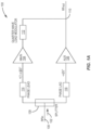
- FIG. 1A is a Doherty amplifier 100, in accordance with some embodiments.
- the Doherty amplifier 100 is an integrated circuit (IC) or a module amplification device. In some embodiments, the Doherty amplifier 100 is a non-inverting Doherty amplifier. The Doherty amplifier 100 is configured to amplify a radio frequency signal 102. The specific characteristics of the Doherty amplifier 100 may vary in accordance with the communication device and technological environment in which the Doherty amplifier 100 is employed and, in addition, the performance parameters relevant to the operation of the Doherty amplifier 100 for the particular application(s) of the Doherty amplifier 100 within the communication device (or prospective communication device(s)) and the technological environment (or prospective technological environment(s)). It should be noted that the Doherty amplifier 100 may be configured for operation in any suitable communication device and technological environment. Thus, the RF signal 102 may be any type of RF signal.
- the Doherty amplifier is particularly useful when the RF signal 102 is a modulated RF signal.
- the amplification techniques explained below are particularly useful so that a main amplifier 104 and an auxiliary amplifier 106 in the Doherty amplifier 100 can maintain high efficiency with a modulated RF signal over a wide frequency band.
- the RF signal 102 may be multiplexed using time division multiplexing (TDM), frequency division multiplexing (FDM), space division multiplexing (SDM), code division multiple access (CDMA) multiplexing, orthogonal frequency division multiple access (OFDMA) multiplexing, and/or the like.
- TDM time division multiplexing
- FDM frequency division multiplexing
- SDM space division multiplexing
- CDMA code division multiple access
- OFDMA orthogonal frequency division multiple access
- the Doherty amplifier 100 may be configured to provide amplification for the RF signal 102 if the RF signal 102 is formatted in accordance with 2G Global System for Mobile Communications (GSM) standards, 3G standards, 3G Long Term Evolution (LTE) standards, 5G standards, 5G New Radio (NR) standards, 6G standards, and/or the like.
- GSM Global System for Mobile Communications
- LTE Long Term Evolution
- NR 5G standards
- 6G standards 6G standards
- the RF signal 102 is provided in a frequency range that is defined by a third generation partnership project (3GPP) or a federal communications commission (FCC).
- the RF signal 102 may be an RF uplink signal for uplink to a base station from a mobile communication device (e.g., smartphone, tablet, laptop, etc.).
- the Doherty amplifier 100 may be within the mobile communication device and the mobile communication device may be using the Doherty amplifier 100 to amplify the RF signal 102 for transmission by an antenna (not shown). Alternatively, the Doherty amplifier 100 may be within the base station. Thus, the base station may be using the Doherty amplifier 100 for amplification upon reception of the RF signal 102 from the mobile communication device.
- the RF signal 102 may be an RF downlink signal for downlink to the mobile communication device (e.g., smartphone, tablet, laptop, etc.) from the base station.
- the mobile communication device may be using the Doherty amplifier 100 to amplify the RF signal 102 after reception from the base station.
- the base station may be using the Doherty amplifier 100 to amplify the RF signal 102 for transmission by an antenna (not shown) to the mobile communication device.
- the Doherty amplifier 100 includes the main amplifier 104 and the auxiliary amplifier 106. While a signal level of the RF signal 102 is below a threshold level, the auxiliary amplifier 106 is deactivated and the main amplifier 104 provides all of the amplification to the RF signal 102. In some embodiments, the threshold level corresponds with an average power level of amplification.
- the RF signal 102 may be any type of RF signal depending on the type of communication device (e.g., smartphone, tablet, laptop, base station, etc.) in which the Doherty amplifier 100 is provided and the amplification operation being provided by the Doherty amplifier 100.
- the main amplifier 104 is configured to amplify the RF signal 102 in accordance with gain of the main amplifier 104. So long as the main amplifier 104 is within a linear operating range (i.e., not saturated and below a compression point), the auxiliary amplifier 106 is deactivated. In some embodiments, the main amplifier 104 is biased so as to be a class AB amplifier or a class B amplifier.
- the output impedance of the auxiliary amplifier 106 is very high and the auxiliary amplifier 106 appears like an open circuit with respect to the main amplifier 104 while the main amplifier 104 is activated and the auxiliary amplifier 106 is deactivated.
- the auxiliary amplifier 106 is configured to activate in response to the signal level of the RF signal 102 reaching a threshold level (e.g., the signal level corresponding to the average power level).
- the Doherty amplifier 100 is configured such that the main amplifier 104 remains activated while the auxiliary amplifier 106 is activated.
- the main amplifier 104 may be held at or near its peak power level (i.e., saturation). In general, this peak power level occurs just prior to the 3dB compression point (i.e., a knee voltage) of the main amplifier 104 and thus when the main amplifier 104 is nearly saturated.
- the Doherty amplifier 100 may hold the main amplifier 104 at backed-off power levels while the auxiliary amplifier 106 is activated. If the Doherty amplifier 100 holds the main amplifier 104 at backed-off power levels while the auxiliary amplifier 106 is activated, a control circuit may be configured to reduce or prevent power-efficiency degradations in the Doherty amplifier 100 due to the main amplifier 104 operating at power levels backed off from the 3dB compression point. This is typically desirable for modern communication systems.
- the auxiliary amplifier 106 is biased as a class C amplifier.
- the Doherty amplifier 100 includes an RF input 108 (also referred to as an RF input node 108), a splitter 109, an RF output 110 (also referred to as an RF output node), a quarter wave component 112, and a phase lead component 114, and a phase lag component 116.
- the RF signal 102 is received by the Doherty amplifier 100 at the RF input 108.
- the RF input 108 is connected to an input terminal of the splitter 109.
- the input of the main amplifier 104 is connected to one of the splitter output terminals of the splitter 109.
- the input of the auxiliary amplifier 106 is coupled to the other splitter output terminal of the splitter 108. Both the main amplifier input of the main amplifier 104 and the auxiliary amplifier input of the auxiliary amplifier 106 are coupled to the RF input 108 through the splitter 109.
- the RF input 108 is a node, a pin, a terminal, a port, a contact, a conductive pillar, a trace, or any other component capable of receiving the RF signal 102. Both the main amplifier output of the main amplifier 104 and the auxiliary amplifier output of the auxiliary amplifier 106 are coupled to the RF output 110. In some embodiments, the RF input 108 is a node, a pin, a terminal, a port, a contact, a conductive pillar, a trace, or any other component capable of transmitting the RF signal 102 to a load.
- the quarter wave component 112 is coupled between the main amplifier output of the main amplifier 104 and the RF output 110.
- the quarter wave component 112 is configured to provide a 90 degree phase shift.
- the quarter wave component 112 is a quarter wave transmission line transformer.
- the quarter wave component 112 is a quadrature coupler.
- the splitter 109 and the quarter wave component 116 are, collectively, a quadrature coupler.
- the main amplifier 104 is the only amplifier that provides amplification to the RF signal 102.
- the quarter wave component 112 provides a 90 degree phase shift to the amplified RF signal 102 at a designed frequency.
- the RF signal 102 is split at the RF input 108. In some embodiment, the RF input 108 is split evenly. In other embodiments, the RF signal 102 is not split evenly.
- the split RF signals are out of phase. Under ideal operating conditions, split RF signals are brought back into phase and constructively combined by the quarter wave component 112.
- the components in the Doherty amplifier 100 each have different phase shifts throughout the frequency band of the frequency band and thus without the phase lead component 114 and the phase lag component 116 and thus the split RF signal are only brought back into phase at a single frequency or at a narrow set of frequencies.
- the phase lead component 114 and the phase lag component 116 are provided so as that the split RF signals are brought back into phase and constructively combined on a much wider frequency range, such as a frequency band defined by 3GPP or the FCC.
- the phase lead component 114 is coupled between one of the output terminals of the splitter 109 and an input of the main amplifier 104.
- the phase lead component 114 is configured to provide a positive phase shift such that the phase shift is equal to +(1- ⁇ ) ⁇ at the input of the main amplifier 104.
- the phase lag component 116 is coupled between the other output terminal of the splitter and an input of the auxiliary amplifier 106.
- the phase lag component 116 is configured to provide a negative phase shift such that the phase shift at the input terminal at the input of the auxiliary amplifier is equal to - ⁇ ( ⁇ ).
- ⁇ is a parameter slope of a phase difference in phase between the input of the main amplifier 104 and the input of the auxiliary amplifier 106 throughout the frequency band. The parameter ⁇ is explained in further detail below.
- ⁇ is a parameter that determines the phase difference in phase between the input of the main amplifier and the input of the auxiliary amplifier at a center frequency of the frequency band.
- the parameter ⁇ is further explained below.
- the phase shift provided by the splitter 108 at both the output terminals is negligible.
- the phase shift provided by the phase lead component is +(1- ⁇ ) ⁇ and the phase shift provided by the phase lag component 116 is - ⁇ ( ⁇ ).
- the ⁇ is selected so that the phase shifts provided by the phase lead component 114 and the phase lag component 116 are maintained constant throughout the frequency band.
- the main amplifier 104 and the auxiliary amplifier 106 may have a frequency response that is not constant throughout the frequency range.
- the parameter ⁇ is selected to compensate for the phase shift provided by the main amplifier 104 and the auxiliary amplifier 106 throughout the frequency band.
- a phase shift of the phase lead component 114 and the phase shift of the phase lag component 116 are such that a maximum output power at the RF output of the Doherty amplifier resulting from power of the main amplifier 104 and power from the auxiliary amplifier 106 is between plus or minus .5dB of a target power over the frequency band.
- the target power is specified by the application of the Doherty amplifier 100.
- the frequency band is defined by 3GPP or the FCC.
- FIG. 1B is a Doherty amplifier 150, in accordance with some embodiments.
- the Doherty amplifier 150 is an integrated circuit or a module amplification device.
- the Doherty amplifier 150 is an inverted Doherty amplifier.
- the Doherty amplifier 150 is configured to amplify the RF signal 102.
- the specific characteristics of the Doherty amplifier 150 may vary in accordance with the communication device and technological environment in which the Doherty amplifier 150 is employed and, in addition, the performance parameters relevant to the operation of the Doherty amplifier 150 for the particular application(s) of the Doherty amplifier 150 within the communication device (or prospective communication device(s)) and the technological environment (or prospective technological environment(s)). It should be noted that the Doherty amplifier 150 may be configured for operation in any suitable communication device and technological environment.
- the Doherty amplifier 150 includes the RF input 108, the RF output 110, the main amplifier 104 and the auxiliary amplifier 106 described above with respect to FIG. 1A .
- the Doherty amplifier 150 includes the main amplifier 104 and the auxiliary amplifier 106. While a signal level of the RF signal 102 is below a threshold level, the auxiliary amplifier 106 is deactivated and the main amplifier 104 provides all of the amplification to the RF signal 102.
- the threshold level corresponds with an average power level of amplification.
- the RF signal 102 may be any type of RF signal depending on the type of communication device (e.g., smartphone, tablet, laptop, base station, etc.) in which the Doherty amplifier 150 is provided and the amplification operation being provided by the Doherty amplifier 150.
- the main amplifier 104 is configured to amplify the RF signal 102 in accordance with the gain of the main amplifier 104. So long as the main amplifier 104 is within a linear operating range (i.e., not saturated and below a compression point), the auxiliary amplifier 106 is deactivated. In some embodiments, the main amplifier 104 is biased so as to be a class AB amplifier or a class B amplifier.
- the output impedance of the auxiliary amplifier 106 is very high and the auxiliary amplifier 106 appears like an open circuit with respect to the main amplifier 104 while the main amplifier 104 is activated and the auxiliary amplifier 106 is deactivated.
- the auxiliary amplifier 106 is configured to activate in response to the signal level of the RF signal 102 reaching a threshold level (e.g., the signal level corresponding to the average power level).
- the Doherty amplifier 150 is configured such that the main amplifier 104 remains activated while the auxiliary amplifier 106 is activated.
- the main amplifier 104 may be held at or near its peak power level (i.e., saturation). In general, this peak power level occurs just prior to the 3dB compression point (i.e., a knee voltage) of the main amplifier 104 and thus when the main amplifier 104 is nearly saturated.
- the Doherty amplifier 150 may hold the main amplifier 104 at backed-off power levels while the auxiliary amplifier 106 is activated. If the Doherty amplifier 150 holds the main amplifier 104 at backed-off power levels while the auxiliary amplifier 106 is activated, a control circuit may be configured to reduce or prevent power-efficiency degradations in the Doherty amplifier 150 due to the main amplifier 104 operating at power levels backed off from the 3dB compression point. This is typically desirable for modern communication systems.
- the auxiliary amplifier 106 is biased as a class C amplifier.
- the Doherty amplifier 150 includes the phase lead component 114, the phase lag component 116, a quarter wave component 154, a matching network 156, and a delay component 158.
- the RF signal 102 is received by the Doherty amplifier 150 at the RF input 108.
- the RF input 108 is connected to a splitter 109.
- the input of the main amplifier 104 is connected to one of the splitter output terminals of the splitter 109.
- the input of the auxiliary amplifier 106 is coupled to the other splitter output terminal of the splitter 109. Both the main amplifier input of the main amplifier 104 and the auxiliary amplifier input of the auxiliary amplifier 106 are coupled to the RF input 108 through the splitter 109.
- the RF input 108 is a node, a pin, a terminal, a port, a contact, a conductive pillar, a trace, or any other component capable of receiving the RF signal 102. Both the main amplifier output of the main amplifier 104 and the auxiliary amplifier output of the auxiliary amplifier 106 are coupled to the RF output 110. In some embodiments, the RF input 108 is a node, a pin, a terminal, a port, a contact, a conductive pillar, a trace, or any other component capable of transmitting the RF signal 102 to a load.
- the quarter wave component 154 is coupled between amplifier output of the main amplifier 104 and the RF output 110.
- the quarter wave component 154 is configured to provide a 90 degree phase shift.
- the quarter wave component 154 is a quarter wave transmission line transformer.
- the quarter wave component 154 is a quadrature coupler.
- the matching network 156 is coupled between the output terminal of the auxiliary amplifier 106 and the delay component 158.
- the delay component is coupled between the matching network 156 and the RF output 110.
- the matching network 156 and delay component 158 are configured to match the load impedance to the impedance of the auxiliary amplifier and provide the appropriate phase shift at the RF output node 110. Under ideal operating conditions, split RF signals are brought back into phase and constructively combined by the quarter wave component 154, the matching network 156, and the delay component 158.
- the components in the Doherty amplifier 150 each have different phase shifts throughout the frequency band of the frequency band and thus without the phase lead component 114 and the phase lag component 116 and thus the split RF signal are only brought back into phase at a single frequency or at a narrow set of frequencies.
- the phase lead component 114 and the phase lag component 116 are provided so as that the split RF signals are brought back into phase and constructively combined on a much wider frequency range, such as a frequency band defined by 3GPP or the FCC.
- the phase lead component 114 is coupled between one of the output terminals of the splitter 109 and an input of the auxiliary amplifier 106.
- the phase lead component 114 is configured to provide a positive phase shift such that the phase shift is equal to +(1- ⁇ ) ⁇ at the input of the main amplifier 104.
- the phase lag component 116 is coupled between the other output terminal of the splitter and an input of the main amplifier 104.
- the phase lag component 116 is configured to provide a negative phase shift such that the phase shift at the input terminal at the input of the auxiliary amplifier is equal to - ⁇ ( ⁇ ).
- ⁇ is a parameter slope of a phase difference in phase between the input of the main amplifier 104 and the input of the auxiliary amplifier 106 throughout the frequency band.
- ⁇ is a parameter that determines the phase difference in phase between the input of the main amplifier 104 and the input of the auxiliary amplifier 106 at a center frequency (i.e., 3.7 GHz in FIG. 3 ) of the frequency band.
- the parameter ⁇ is further explained below.
- the phase shift provided by the splitter 108 at both the output terminals is negligible.
- the phase shift provided by the phase lead component 114 is +(1- ⁇ ) ⁇ and the phase shift provided by the phase lag component 116 is - ⁇ ( ⁇ ).
- the ⁇ is selected so that the phase shifts provided by the phase lead component 114 and the phase lag component 116 are maintained constant throughout the frequency band.
- the main amplifier 104 and the auxiliary amplifier 106 may have a frequency response that is not constant throughout the frequency range.
- the parameter ⁇ is selected to compensate for the phase shift provided by the main amplifier 104 and the auxiliary amplifier 106 throughout the frequency band.
- a phase shift of the phase lead component 114 and the phase shift of the phase lag component 116 are such that a maximum output power at the RF output of the Doherty amplifier resulting from power of the main amplifier 104 and power from the auxiliary amplifier 106 is between plus or minus .5dB of a target power over the frequency band.
- the target power is specified by the application of the Doherty amplifier 100.
- the frequency band is defined by 3GPP or the FCC.
- the phase lead component 114 is usually realized by a L-C-L pi-network, or a series C- shunt L network.
- the phase lag component 116 is realized with a transmission line, a C-L-C pi-network, or a series L- shunt C network.
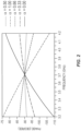
- FIG. 2 is a plot that illustrates the phase difference between the input at the main amplifier 104 ( See FIG. 1B ) and the input of the auxiliary amplifier 106 (See FIG. 1B ) in an inverted Doherty amplifier (see FIG. 1B ) as a function of frequency, in accordance with some embodiments.
- FIG. 2 is a plot that illustrates the phase difference between the input at the auxiliary amplifier 106 (See FIG. 1A ) and the input of the main amplifier 104 (See FIG. 1A ) in a non-inverted Doherty amplifier (see FIG. 1A ) as a function of frequency, in accordance with some embodiments.
- phase difference lines correspond to the phase difference wherein for each of the phase difference lines, the parameter ⁇ is selected to be 90 degrees. However, each of the lines has a different value of the parameter ⁇ .
- the phase difference lines correspond to the phase difference at different frequencies along a frequency band between 3.2GHz and 4.2GHz. Phase difference lines are provided for values of the parameter ⁇ at 0, .33, .5, .66. and 1. Note that at the center frequency of 3.7GHz, the value of each of the phase difference lines is 90 degrees. This is because the parameter ⁇ is equal to 90 degrees for each of the phase difference lines. Also note that for each of the values of the parameter ⁇ at 0, .33, .5, .66. and 1, the phase differences are substantially linear throughout the frequency band.
- the phase difference line is maintained at approximately 90 degrees throughout the frequency band, as shown in FIG. 2 .
- the main amplifier 104 See FIG. 1A and FIG. 1B
- the auxiliary amplifier 106 See FIG. 1A and FIG. 1B
- setting the parameter ⁇ equal to .5 result in the phase lead component 114 and the phase lag component 116 being provided so as that the split RF signals output from the main amplifier 104 and the auxiliar amplifier 106 are brought back into phase and constructively combined at the RF output 110 throughout the frequency band.
- the main amplifier 104, the auxiliary amplifier 106, the quarter wave component 154, the matching network 156 (in the Doherty amplifier 150), and/or the delay component 158 (in the Doherty amplifier 150) have phases that vary throughout the frequency band.
- the parameter ⁇ is selected so that the split RF signals output from the main amplifier 104 and the auxiliar amplifier 106 are brought back into phase and constructively combined at the RF output 110 throughout the frequency band.
- phase lead component 114 and the phase lag component 116 compensate for the variation in phase of the other components in the Doherty amplifiers 100, 150 to ensure that the split RF signals output from the main amplifier 104 and the auxiliar amplifier 106 are brought back into phase and constructively combined at the RF output 110 throughout the frequency band. This ensures that the Doherty amplifiers 100, 150 operate throughout much larger frequency bands.
- the parameter ⁇ when the parameter ⁇ is selected to be less than .5, the phase difference lines have a positive slope. Also note that when the parameter ⁇ is selected to be greater than .5, the phase difference lines have a negative slope. Also note that while the parameter ⁇ is equal to 90 degrees in the examples shown herein, the parameter ⁇ can be equal to any other value thereby moving the value of the phase difference lines at the center frequency to higher phase values or lower phase values in accordance with a desired design.
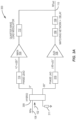
- FIG. 3A is a Doherty amplifier 300, in accordance with some embodiments.
- the Doherty amplifier 300 is an IC or a module amplification device.
- the Doherty amplifier 300 is a non-inverting Doherty amplifier.
- the Doherty amplifier 300 is similar to the non-inverting Doherty amplifier 100 shown in FIG. 1A .
- the components that are different between Doherty amplifier 300 and the Doherty amplifier 100 are to be discussed while all other components are presumed to operate in the same manner.
- the Doherty amplifier 300 includes a hybrid coupler 309 instead of a splitter 109 (See FIG. 1A ).
- the RF input 108 is coupled to a first terminal of the hybrid coupler 309.
- a terminating impedance 311 e.g., 50 Ohm impedance
- the phase lead component 114 is coupled in series between a third terminal of the hybrid coupler 309 and an input of the main amplifier 104.
- the phase lead component 114 in FIG. 3A is configured to provide a positive phase shift such that the phase shift is equal to +(1 - ⁇ ) ⁇ at the input of the main amplifier 104.
- the phase lead component 114 in FIG. 3A has the phase shift equal to +(1- ⁇ ) ⁇ at the input of the main amplifier 104 since the phase difference between the first terminal of the hybrid coupler 309 coupled to the RF input 108 and the third terminal of the hybrid coupler 309 coupled to the input of the main amplifier 104 is zero degrees.
- a phase lag component 316 is coupled in series between a fourth terminal of the hybrid coupler 309 and an input of the auxiliary amplifier 106.
- the phase lag component 316 in FIG. 3A is configured to provide a phase shift such that the phase shift is equal to -90- ⁇ ( ⁇ ) at the input of the auxiliary amplifier 106.
- the phase shift at the input of auxiliary amplifier 106 is not equal to - ⁇ ( ⁇ ). This is because the hybrid coupler 309 provides a negative phase shift of -90 degrees between the first terminal of the hybrid coupler 309 and the fourth terminal of the hybrid coupler 309.
- phase lag component 316 provides a phase shift such that the phase shift of the phase lag component 316 and the -90 degree phase shift provided by the hybrid coupler 309 in combination is equal to -90- ⁇ ( ⁇ ) at the input of the auxiliary amplifier 106.
- a phase shift of the phase lead component 114 and the phase shift of the phase lag component 316 are such that a maximum output power at the RF output 110 of the Doherty amplifier 300 resulting from power of the main amplifier 104 and power from the auxiliary amplifier 106 is between plus or minus .5dB of a target power over the frequency band.
- the target power is specified by the application of the Doherty amplifier 300.
- the frequency band is defined by 3GPP or the FCC.
- FIG. 3B is a Doherty amplifier 350, in accordance with some embodiments.
- the Doherty amplifier 350 is an IC or a module amplification device.
- the Doherty amplifier 300 is a non-inverting Doherty amplifier.
- the Doherty amplifier 300 is similar to the inverting Doherty amplifier 150 shown in FIG. 1B .
- the components that are different between Doherty amplifier 300 and the Doherty amplifier 100 are to be discussed while all other components are presumed to operate in the same manner.
- the Doherty amplifier 300 includes a hybrid coupler 359 instead of a splitter 109 (See FIG. 1B ).
- the RF input 108 is coupled to a first terminal of the hybrid coupler 359.
- a terminating impedance 311 e.g., 50 Ohm impedance
- the phase lead component 114 is coupled in series between a third terminal of the hybrid coupler 359 and an input of the auxiliary amplifier 106.
- the phase lead component 114 in FIG. 3A is configured to provide a positive phase shift such that the phase shift is equal to +(1- ⁇ ) ⁇ at the input of the auxiliary amplifier 106.
- the phase lead component 114 in FIG. 3B has the phase shift equal to +(1- ⁇ ) ⁇ at the input of the auxiliary amplifier 106 since the phase difference between the first terminal of the hybrid coupler 359 coupled to the RF input 108 and the third terminal of the hybrid coupler 359 coupled to the input of the auxiliary amplifier 106 is zero degrees.
- a phase lag component 316 is coupled in series between a fourth terminal of the hybrid coupler 359 and an input of the main amplifier 104.
- the phase lag component 316 in FIG. 3B is configured to provide a phase shift such that the phase shift is equal to -90- ⁇ ( ⁇ ) at the input of the main amplifier 106.
- the phase shift at the input of main amplifier 104 is not equal to - ⁇ ( ⁇ ) This is because the hybrid coupler 309 provides a negative phase shift of -90 degrees between the first terminal of the hybrid coupler 359 and the fourth terminal of the hybrid coupler 359.
- phase lag component 316 provides a phase shift such that the phase shift of the phase lag component 316 and the -90 degree phase shift provided by the hybrid coupler 359 in combination is equal to -90- ⁇ ( ⁇ ) at the input of the main amplifier 104.
- a phase shift of the phase lead component 114 and the phase shift of the phase lag component 316 are such that a maximum output power at the RF output 110 of the Doherty amplifier 350 resulting from power of the main amplifier 104 and power from the auxiliary amplifier 106 is between plus or minus .5dB of a target power over the frequency band.
- the target power is specified by the application of the Doherty amplifier 350.
- the frequency band is defined by 3GPP or the FCC.
- FIG. 4 is a phase lead component 400, in accordance with some embodiments.
- the phase lead component 114 in FIG. 1A , 1B , 3A , 3B is provided in the same manner as the phase lead component 400 in FIG. 4 .
- the phase lead component 400 includes an inductor 402, a capacitor 404, an inductor 406, a node 408, and a node 410.
- the node 408 is connected to the corresponding terminal of the splitter 109 (See FIG. 1A , 1B ) or the hybrid coupler 309, 359 (See FIG. 3A , 3B ).
- the node 410 is coupled to the corresponding input of the main amplifier 104 (See FIG. 1A , 3A ) or auxiliary amplifier 106 (See FIG. 1B , 3B ).
- the capacitor 404 is connected between the node 408 and the node 410.
- the inductor 402 is connected in shunt to the node 408.
- the inductor 406 is connected in shunt to the node 410.
- the phase lead component 400 is configured to provide a positive phase shift.
- FIG. 5 is a phase lag component 500, in accordance with some embodiments.
- the phase lag component 116 in FIG. 1A , 1B is provided in the same manner as the phase lag component 500 in FIG. 5 .
- the phase lag component 316 in FIG. 3A , 3B is provided in the same manner as the phase lag component 500 in FIG. 5 .
- the phase lag component 500 includes a capacitor 502, an inductor 504, a capacitor 506, a node 508, and a node 510.
- the node 508 is connected to the corresponding terminal of the splitter 109 (See FIG. 1A , 1B ) or the hybrid coupler 309, 359 (See FIG. 3A , 3B ).
- the node 510 is coupled to the corresponding input of the auxiliary amplifier 106 (See FIG. 1A , 3A ) or main amplifier 104 (See FIG. 1B , 3B ).
- the inductor 504 is connected between the node 508 and the node 510.
- the capacitor 502 is connected in shunt to the node 508.
- the capacitor 506 is connected in shunt to the node 510.
- the phase lag component 500 is configured to provide a negative phase shift.
- FIG. 6A, FIG. 6B, and FIG. 6C illustrate simulation results of a conventional inverted Doherty amplifier and the inverted Doherty amplifier 150 shown in FIG. 1B .
- the parameter ⁇ was selected to be 90 degrees and the parameter ⁇ was selected to be .5 for the inverted Doherty amplifier 150.
- FIG. 6A illustrates the drain efficiency 600A of the conventional inverted Doherty at an average output power of 39dBm and drain efficiency 600B of the inverted Doherty amplifier 150 at an average output power of 39dBm.
- FIG. 6B illustrates the drain efficiency 602A of the conventional inverted Doherty at saturation and drain efficiency 600B of the inverted Doherty amplifier 150 at saturation.
- FIG. 6C illustrates the output power 604A of the conventional inverted Doherty at saturation and output power 604B of the inverted Doherty amplifier 150 at saturation.
- the inverted Doherty amplifier 150 has a 2.5GHz bandwidth (2.1GHz - 4.6GHz) whereas conventional inverted Doherty amplifier has less than 1.3GHz bandwidth (2.8GHz - 4.1 GHz).
- inverted Doherty amplifier 150 has 2.0GHz bandwidth (2.4GHz - 4.4GHz) whereas conventional inverted Doherty amplifier has less than 900MHz bandwidth (2.7GHz - 3.8GHz).
- FIG. 7A and FIG. 7C illustrate simulation result for a conventional Doherty amplifier.
- FIG. 7B and FIG. 7D illustrate simulation results for the inverted Doherty amplifier 150 shown in FIG. 1B .
- FIG. 7A illustrates the drain efficiency of the conventional Doherty amplifier wherein each line represents a different frequency.
- FIG. 7C illustrates the gain of the conventional Doherty amplifier wherein each line represents a different frequency.
- FIG. 7B illustrates the drain efficiency of the inverted Doherty amplifier 150 shown in FIG. 1B wherein each line represents a different frequency.
- FIG. 7D illustrates the gain of the inverted Doherty amplifier 150 shown in FIG. 1B wherein each line represents a different frequency.
- the different frequencies are frequencies from 2.1GHz to 4.8GHz in 200MHz steps.
- the inverted Doherty amplifier 150 shows much better performance in drain efficiency and gain (much less dispersion) at average output power, saturated output power and output power that the conventional inverted Doherty amplifier. Furthermore, the inverted Doherty amplifier 150 shows less dispersion in output power at saturation.
- the simulation results in FIG. 6A-7D clearly show that the inverted Doherty amplifier 150 can improve the operating bandwidth of an inverted Doherty amplifier significantly at saturation and backed-off output power.
- the concepts described above may be implemented in various types of user elements 800, such as mobile terminals, smart watches, tablets, computers, navigation devices, access points, and like wireless communication devices that support wireless communications, such as cellular, wireless local area network (WLAN), Bluetooth, and near field communications.
- user elements 800 such as mobile terminals, smart watches, tablets, computers, navigation devices, access points, and like wireless communication devices that support wireless communications, such as cellular, wireless local area network (WLAN), Bluetooth, and near field communications.
- wireless communications such as cellular, wireless local area network (WLAN), Bluetooth, and near field communications.
- the user element 800 will generally include a control system 802, a baseband processor 804, transmit circuitry 806, receive circuitry 808, antenna switching circuitry 810, multiple antennas 812, and user interface circuitry 814.
- the control system 802 may be a field-programmable gate array (FPGA) or an application-specific integrated circuit (ASIC).
- the control system 802 may include at least a microprocessor(s), an embedded memory circuit(s), and a communication bus interface(s).
- the receive circuitry 808 receives radio frequency signals via the antennas 812 and through the antenna switching circuitry 810 from one or more base stations.
- a low noise amplifier and a filter cooperate to amplify and remove broadband interference from the received signal for processing.
- Downconversion and digitization circuitry (not shown) will then downconvert the filtered, received signal to an intermediate or baseband frequency signal, which is then digitized into one or more digital streams using analog-to-digital converter(s) (ADC(s)).
- ADC(s) analog-to
- the Doherty amplifier 100 of FIG. 1A , the Doherty amplifier 150 of FIG. 1B , the Doherty amplifier 300 of FIG. 3A , and the Doherty amplifier 350 of FIG. 3B are implemented in the user element 800 and, in particular, in the receive circuitry 808 and/or the transmit circuitry 806.
- the baseband processor 804 processes the digitized received signal to extract the information or data bits conveyed in the received signal. This processing typically comprises demodulation, decoding, and error correction operations, as will be discussed in greater detail below.
- the baseband processor 804 is generally implemented in one or more digital signal processors (DSPs) and ASICs.
- DSPs digital signal processors
- the baseband processor 804 receives digitized data, which may represent voice, data, or control information, from the control system 802, which it encodes for transmission.
- the encoded data is output to the transmit circuitry 806, where a digital-to-analog converter(s) (DAC) converts the digitally encoded data into an analog signal and a modulator modulates the analog signal onto a carrier signal that is at a desired transmit frequency or frequencies.
- DAC digital-to-analog converter
- a power amplifier will amplify the modulated carrier signal to a level appropriate for transmission and deliver the modulated carrier signal to the antennas 812 through the antenna switching circuitry 810.
- the multiple antennas 812 and the replicated transmit and receive circuitries 806, 808 may provide spatial diversity. Modulation and processing details will be understood by those skilled in the art.
- a Doherty amplifier includes an RF input of the Doherty amplifier for receiving a radio frequency (RF) signal, a main amplifier coupled to the RF input, and an auxiliary amplifier coupled to the RF input.
- RF radio frequency
- a phase lag component connected between the RF input and one of either the main amplifier or the auxiliary amplifier and a phase lead component connected between the RF input and another one of either the main amplifier or the auxiliary amplifier.
- the phase lead and phase lag components ensure that the split signals output from the main and auxiliary amplifier are recombined in phase throughout a frequency band.
- a Doherty amplifier comprising: a radio frequency (RF) input of the Doherty amplifier for receiving an RF signal; a main amplifier coupled to the RF input; an auxiliary amplifier coupled to the RF input; a phase lag component connected between the RF input and one of either the main amplifier or the auxiliary amplifier; and a phase lead component connected between the RF input and an other one of either the main amplifier or the auxiliary amplifier.
- RF radio frequency
- the Doherty amplifier of clause 2 further comprising: an RF output of the Doherty amplifier for outputting the RF signal after amplification; and a quarter wave component connected between the main amplifier and the RF output of the Doherty amplifier.
- Clause 4 The Doherty amplifier of clause 3, further comprising a splitter having an input terminal, a first output terminal, and a second output terminal, wherein: the input terminal is coupled to the RF input of the Doherty amplifier; the first output terminal is coupled to an input of the main amplifier; and the second output terminal is coupled to an input of the auxiliary amplifier.
- the Doherty amplifier of clause 3 or 4 further comprising a hybrid coupler having a first terminal, a second terminal, a third terminal, and a fourth terminal, wherein: the first terminal is coupled to the RF input of the Doherty amplifier; the second terminal is coupled to ground; the third terminal is coupled to an input of the main amplifier; and the fourth terminal is coupled to an input of the auxiliary amplifier.
- the phase lead component provides a first phase shift such that a phase lead within a frequency band at an input of the main amplifier is equal to +(1- ⁇ ) ⁇ ; and the phase lag component provides a second phase shift such that a phase lag within the frequency band at an input of the auxiliary amplifier is equal to - ⁇ ( ⁇ ) or -90- ⁇ ( ⁇ ), wherein: ⁇ is a parameter slope of a phase difference in phase between the input of the auxiliary amplifier and the input of the main amplifier throughout the frequency band; and ⁇ is a parameter that determines the phase difference in phase between the input of the main amplifier and the input of the auxiliary amplifier at a center frequency of the frequency band.
- Clause 7 The Doherty amplifier of clause 6, wherein the frequency band is defined by a third generation partnership project (3GPP) or a federal communications commission (FCC).
- 3GPP third generation partnership project
- FCC federal communications commission
- Clause 8 The Doherty amplifier of any of clauses 3 to 7, wherein a first phase shift and a second phase shift are set such that a maximum output power at the RF output of the Doherty amplifier, resulting from power of the main amplifier and power from the auxiliary amplifier, is between plus or minus .5dB of a target power over a frequency band.
- the phase lead component provides a first phase shift such that a phase lead within a frequency band at an input of the auxiliary amplifier is equal to +(1- ⁇ ) ⁇ ; and the phase lag component provides a second phase shift such that a phase lag within the frequency band at an input of the main amplifier is equal to - ⁇ ( ⁇ ) or -90- ⁇ ( ⁇ ), wherein: ⁇ is a parameter slope of a phase difference in phase between the input of the main amplifier and the input of the auxiliary amplifier throughout the frequency band; and ⁇ is a parameter that determines the phase difference in phase between the input of the main amplifier and the input of the auxiliary amplifier at a center frequency of the frequency band.
- Clause 14 The Doherty amplifier of clause 13, wherein the frequency band is defined by a third generation partnership project (3GPP) or a federal communications commission (FCC).
- 3GPP third generation partnership project
- FCC federal communications commission
- Clause 15 The Doherty amplifier of any of clauses 10 to 14, wherein a first phase shift and a second phase shift are set such that a maximum output power at the RF output of the Doherty amplifier, resulting from power of the main amplifier and power from the auxiliary amplifier, is between plus or minus .5dB of a target power over a frequency band.
- a Doherty amplifier comprising: a radio frequency (RF) input of the Doherty amplifier for receiving an RF signal; a main amplifier coupled to the RF input; an auxiliary amplifier coupled to the RF input; a phase lag component providing a first phase shift, the phase lag component being connected between the RF input and one of either the main amplifier or the auxiliary amplifier; a phase lead component providing a second phase shift, the phase lead component being connected between the RF input and an other one of either the main amplifier or the auxiliary amplifier; and wherein the first phase shift and the second phase shift are set such that a maximum output power at an RF output of the Doherty amplifier, resulting from power of the main amplifier and power from the auxiliary amplifier, is between plus or minus .5dB of a target power over a frequency band.
- RF radio frequency
- the Doherty amplifier is a non-inverting Doherty amplifier wherein: the phase lead component is connected between the RF input of the Doherty amplifier and the main amplifier; and the phase lag component is connected between the RF input of the Doherty amplifier and the auxiliary amplifier.
- the phase lead component provides the first phase shift such that a phase lead within the frequency band at an input of the main amplifier is equal to +(1- ⁇ ) ⁇ ; and the phase lag component provides the second phase shift such that a phase lag within the frequency band at an input of the auxiliary amplifier is equal to - ⁇ ( ⁇ ) or -90- ⁇ ( ⁇ ), wherein: ⁇ is a parameter slope of a phase difference in phase between the input of the auxiliary amplifier and the input of the main amplifier throughout the frequency band; and ⁇ is a parameter that determines the phase difference in phase between the input of the main amplifier and the input of the auxiliary amplifier at a center frequency of the frequency band.
- the Doherty amplifier is an inverting Doherty amplifier wherein: the phase lead component is connected between the RF input of the Doherty amplifier and the auxiliary amplifier; and the phase lag component is connected between the RF input of the Doherty amplifier and the main amplifier.
- the phase lead component provides the first phase shift such that a phase lead within the frequency band at an input of the auxiliary amplifier is equal to +(1- ⁇ ) ⁇ ; and the phase lag component provides the second phase shift such that a phase lag within the frequency band at an input of the main amplifier is equal to - ⁇ ( ⁇ ) or -90- ⁇ ( ⁇ ), wherein: ⁇ is a parameter slope of a phase difference in phase between the input of the main amplifier and the input of the auxiliary amplifier throughout the frequency band; and ⁇ is a parameter that determines the phase difference in phase between the input of the main amplifier and the input of the auxiliary amplifier at a center frequency of the frequency band.
Landscapes
- Engineering & Computer Science (AREA)
- Power Engineering (AREA)
- Microelectronics & Electronic Packaging (AREA)
- Amplifiers (AREA)
Abstract
This disclosure relates generally to Doherty amplifiers. In one embodiment, a Doherty amplifier includes an RF input of the Doherty amplifier for receiving a radio frequency (RF) signal, a main amplifier (104) coupled to the RF input, and an auxiliary amplifier (106) coupled to the RF input. A phase lag component (116) connected between the RF input and one of either the main amplifier (104) or the auxiliary amplifier (106) and a phase lead component (114) connected between the RF input and another one of either the main amplifier (104) or the auxiliary amplifier (106). In some embodiments, the phase lead and phase lag components (114, 116) ensure that the split signals output from the main and auxiliary amplifiers (104, 106) are recombined in phase throughout a frequency band.
Description
- This application claims the benefit of provisional patent application serial number
63/539,384, filed September 20, 2023 - This application claims the benefit of provisional patent application serial number
63/513,974, filed July 17, 2023 63/511,352, filed June 30, 2023 63/502,268, filed May 15, 2023 63/479,790, filed January 13, 2023 63/479,788, filed January 13, 2023 63/479,787, filed January 13, 2023 - This disclosure relates generally to Doherty amplifiers formed in integrated circuit (IC) structures.
- Doherty amplifiers are popular for having high efficiency at average output power as well as maximum output power. A Doherty amplifier generally includes a main amplifier (also known as a carrier amplifier) and an auxiliary amplifier (also known as a peaking amplifier). The main and auxiliary amplifiers are biased differently, such that the main amplifier is always providing amplification to a radio frequency (RF) signal while the auxiliary amplifier only provides amplification once the RF signal reaches a particular power level. Doherty amplifiers typically show high efficiency at average power when operating with modulated signal. However, the efficiency of currently known Doherty amplifiers degrades when amplifying a wideband modulated RF signal (e.g., a 5G New Radio (NR) signal with 560MHz bandwidth).
- Particular aspects are set out in the appended independent claims. Various optional embodiments are set out in the dependent claims.
- In some embodiments, a Doherty amplifier, includes: a radio frequency (RF) input of the Doherty amplifier for receiving an RF signal; a main amplifier coupled to the RF input; an auxiliary amplifier coupled to the RF input; a phase lag component connected between the RF input and one of either the main amplifier or the auxiliary amplifier; and a phase lead component connected between the RF input and another one of either the main amplifier or the auxiliary amplifier. In some embodiments, the Doherty amplifier is a non-inverting Doherty amplifier wherein: the phase lead component is connected between the RF input of the Doherty amplifier and the main amplifier; and the phase lag component is connected between the RF input of the Doherty amplifier and the auxiliary amplifier. In some embodiments, the Doherty amplifier further includes: an RF output of the Doherty amplifier for outputting the RF signal after amplification; and a quarter wave component connected between the main amplifier and the RF output of the Doherty amplifier. In some embodiments, the Doherty amplifier further includes a splitter having an input terminal, a first output terminal, and a second output terminal, wherein: the input terminal is coupled to the RF input of the Doherty amplifier; the first output terminal is coupled to an input of the main amplifier; and the second output terminal is coupled to an input of the auxiliary amplifier. In some embodiments, the Doherty amplifier further includes a hybrid coupler having a first terminal, a second terminal, a third terminal, and a fourth terminal, wherein: the first terminal is coupled to the RF input of the Doherty amplifier; the second terminal is coupled to ground; the third terminal is coupled to an input of the main amplifier; and the fourth terminal is coupled to an input of the auxiliary amplifier. In some embodiments, the phase lead component provides a first phase shift such that a phase lead within a frequency band at an input of the main amplifier is equal to +(1-α)β; and the phase lag component provides a second phase shift such that a phase lag within the frequency band at an input of the auxiliary amplifier is equal to -α(β) or -90- α(β), wherein: α is a parameter slope of a phase difference in phase between the input of the auxiliary amplifier and the input of the main amplifier throughout the frequency band; and β is a parameter that determines the phase difference in phase between the input of the main amplifier and the input of the auxiliary amplifier at a center frequency of the frequency band. In some embodiments, the frequency band is defined by a third generation partnership project (3GPP) or a federal communications commission (FCC). In some embodiments, a first phase shift and a second phase shift are set such that a maximum output power at the RF output of the Doherty amplifier, resulting from power of the main amplifier and power from the auxiliary amplifier, is between plus or minus .5dB of a target power over a frequency band. In some embodiments, the Doherty amplifier is an inverting Doherty amplifier wherein: the phase lead component is connected between the RF input of the Doherty amplifier and the auxiliary amplifier; and the phase lag component is connected between the RF input of the Doherty amplifier and the main amplifier. In some embodiments, the Doherty amplifier further includes: an RF output of the Doherty amplifier for outputting the RF signal after amplification; and a quarter wave component connected between the main amplifier and the RF output of the Doherty amplifier. In some embodiments, the Doherty amplifier further includes a splitter having an input terminal, a first output terminal, and a second output terminal, wherein: the input terminal is coupled to the RF input of the Doherty amplifier; the first output terminal is coupled to an input of the main amplifier; and the second output terminal is coupled to an input of the auxiliary amplifier. In some embodiments, the Doherty amplifier further includes a hybrid coupler having a first terminal, a second terminal, a third terminal, and a fourth terminal, wherein: the first terminal is coupled to the RF input of the Doherty amplifier; the second terminal is coupled to ground; the third terminal is coupled to an input of the main amplifier; and the fourth terminal is coupled to an input of the auxiliary amplifier. In some embodiments,: the phase lead component provides a first phase shift such that a phase lead within a frequency band at an input of the auxiliary amplifier is equal to +(1-α)β; and the phase lag component provides a second phase shift such that a phase lag within the frequency band at an input of the main amplifier is equal to -α(β) or -90- α(β), wherein: α is a parameter slope of a phase difference in phase between the input of the main amplifier and the input of the auxiliary amplifier throughout the frequency band; and β is a parameter that determines the phase difference in phase between the input of the main amplifier and the input of the auxiliary amplifier at a center frequency of the frequency band. In some embodiments, the frequency band is defined by a third generation partnership project (3GPP) or a federal communications commission (FCC). In some embodiments, a first phase shift and a second phase shift are set such that a maximum output power at the RF output of the Doherty amplifier, resulting from power of the main amplifier and power from the auxiliary amplifier, is between plus or minus .5dB of a target power over a frequency band.
- In some embodiments, a Doherty amplifier, includes: a radio frequency (RF) input of the Doherty amplifier for receiving an RF signal; a main amplifier coupled to the RF input; an auxiliary amplifier coupled to the RF input; a phase lag component providing a first phase shift, the phase lag component being connected between the RF input and one of either the main amplifier or the auxiliary amplifier; a phase lead component providing a second phase shift, the phase lead component being connected between the RF input and another one of either the main amplifier or the auxiliary amplifier; and wherein the first phase shift and the second phase shift are set such that a maximum output power at an RF output of the Doherty amplifier, resulting from power of the main amplifier and power from the auxiliary amplifier, is between plus or minus .5dB of a target power over a frequency band. In some embodiments, the Doherty amplifier is a non-inverting Doherty amplifier wherein: the phase lead component is connected between the RF input of the Doherty amplifier and the main amplifier; and the phase lag component is connected between the RF input of the Doherty amplifier and the auxiliary amplifier. In some embodiments, the phase lead component provides the first phase shift such that a phase lead within the frequency band at an input of the main amplifier is equal to +(1-α)β; and the phase lag component provides the second phase shift such that a phase lag within the frequency band at an input of the auxiliary amplifier is equal to -α(β) or -90- α(β), wherein: α is a parameter slope of a phase difference in phase between the input of the auxiliary amplifier and the input of the main amplifier throughout the frequency band; and β is a parameter that determines the phase difference in phase between the input of the main amplifier and the input of the auxiliary amplifier at a center frequency of the frequency band. In some embodiments, the Doherty amplifier is an inverting Doherty amplifier wherein: the phase lead component is connected between the RF input of the Doherty amplifier and the auxiliary amplifier; and the phase lag component is connected between the RF input of the Doherty amplifier and the main amplifier. In some embodiments, the phase lead component provides the first phase shift such that a phase lead within the frequency band at an input of the auxiliary amplifier is equal to +(1-α)β; and the phase lag component provides the second phase shift such that a phase lag within the frequency band at an input of the main amplifier is equal to -α(β) or -90- α(β), wherein: α is a parameter slope of a phase difference in phase between the input of the main amplifier and the input of the auxiliary amplifier throughout the frequency band; and β is a parameter that determines the phase difference in phase between the input of the main amplifier and the input of the auxiliary amplifier at a center frequency of the frequency band.
- In another aspect, any of the foregoing aspects individually or together, and/or various separate aspects and features as described herein, may be combined for additional advantage. Any of the various features and elements as disclosed herein may be combined with one or more other disclosed features and elements unless indicated to the contrary herein.
- Those skilled in the art will appreciate the scope of the present disclosure and realize additional aspects thereof after reading the following detailed description of the illustrative embodiments in association with the accompanying drawing figures.
- The accompanying drawing figures incorporated in and forming a part of this specification illustrate several aspects of the disclosure, and together with the description serve to explain the principles of the disclosure:
-
FIG. 1A is a non-inverted Doherty amplifier, in accordance with some embodiments; -
FIG. 1B is an inverted Dohertyamplifier 150, in accordance with some embodiments; -
FIG. 2 is a plot that illustrates the phase difference between the input of a main amplifier and the input of an auxiliary amplifier as a function of frequency, in accordance with some embodiments; -
FIG. 3A is another non-inverted Doherty amplifier, in accordance with some embodiments; -
FIG. 3B is another inverted Doherty amplifier, in accordance with some embodiments; -
FIG. 4 is a phase lead component, in accordance with some embodiments; -
FIG. 5 is a phase lag component, in accordance with some embodiments; -
FIG. 6A illustrates the drain efficiency of the conventional inverted Doherty at an average output power of 39dBm and drain efficiency of the inverted Doherty amplifier shown inFIG. 1B at an average output power of 39dBm, in accordance with some embodiments; -
FIG. 6B illustrates the drain efficiency 602A of the conventional inverted Doherty at saturation and drain efficiency 600B of the inverted Doherty amplifier shown inFIG. 1B at saturation, in accordance with some embodiments; -
FIG. 6C illustrates the output power 604A of the conventional inverted Doherty at saturation and output power 604B of the inverted Doherty amplifier shown inFIG. 1B at saturation, in accordance with some embodiments; -
FIG. 7A illustrates the drain efficiency of the conventional Doherty amplifier, wherein each line represents a different frequency, in accordance with some embodiments; -
FIG. 7B illustrates the gain of the conventional Doherty amplifier, wherein each line represents a different frequency, in accordance with some embodiments; -
FIG. 7C illustrates the drain efficiency of the inverted Doherty amplifier shown inFIG. 1B , wherein each line represents a different frequency, in accordance with some embodiments; -
FIG. 7D illustrates the gain of the inverted Doherty amplifier shown inFIG. 1B , wherein each line represents a different frequency, in accordance with some embodiments; and -
FIG. 8 is a user element, in accordance with some embodiments. - The embodiments set forth below represent the necessary information to enable those skilled in the art to practice the embodiments and illustrate the best mode of practicing the embodiments. Upon reading the following description in light of the accompanying drawing figures, those skilled in the art will understand the concepts of the disclosure and will recognize applications of these concepts not particularly addressed herein. It should be understood that these concepts and applications fall within the scope of the disclosure and the accompanying claims.
- It will be understood that, although the terms first, second, etc. may be used herein to describe various elements, these elements should not be limited by these terms. These terms are only used to distinguish one element from another. For example, a first element could be termed a second element, and, similarly, a second element could be termed a first element, without departing from the scope of the present disclosure. As used herein, the term "and/or" includes any and all combinations of one or more of the associated listed items.
- It will be understood that when an element such as a layer, region, or substrate is referred to as being "on" or extending "onto" another element, it can be directly on or extend directly onto the other element or intervening elements may also be present. In contrast, when an element is referred to as being "directly on" or extending "directly onto" another element, there are no intervening elements present. Likewise, it will be understood that when an element such as a layer, region, or substrate is referred to as being "over" or extending "over" another element, it can be directly over or extend directly over the other element or intervening elements may also be present. In contrast, when an element is referred to as being "directly over" or extending "directly over" another element, there are no intervening elements present. It will also be understood that when an element is referred to as being "connected" or "coupled" to another element, it can be directly connected or coupled to the other element or intervening elements may be present. In contrast, when an element is referred to as being "directly connected" or "directly coupled" to another element, there are no intervening elements present.
- Relative terms such as "below" or "above" or "upper" or "lower" or "horizontal" or "vertical" may be used herein to describe a relationship of one element, layer, or region to another element, layer, or region as illustrated in the Figures. It will be understood that these terms and those discussed above are intended to encompass different orientations of the device in addition to the orientation depicted in the Figures.
- The terminology used herein is for the purpose of describing particular embodiments only and is not intended to be limiting of the disclosure. As used herein, the singular forms "a," "an," and "the" are intended to include the plural forms as well, unless the context clearly indicates otherwise. It will be further understood that the terms "comprises," "comprising," "includes," and/or "including" when used herein specify the presence of stated features, integers, steps, operations, elements, and/or components, but do not preclude the presence or addition of one or more other features, integers, steps, operations, elements, components, and/or groups thereof.
- Unless otherwise defined, all terms (including technical and scientific terms) used herein have the same meaning as commonly understood by one of ordinary skill in the art to which this disclosure belongs. It will be further understood that terms used herein should be interpreted as having a meaning that is consistent with their meaning in the context of this specification and the relevant art and will not be interpreted in an idealized or overly formal sense unless expressly so defined herein.
- Embodiments are described herein with reference to schematic illustrations of embodiments of the disclosure. As such, the actual dimensions of the layers and elements can be different, and variations from the shapes of the illustrations as a result, for example, of manufacturing techniques and/or tolerances, are expected. For example, a region illustrated or described as square or rectangular can have rounded or curved features, and regions shown as straight lines may have some irregularity. Thus, the regions illustrated in the figures are schematic and their shapes are not intended to illustrate the precise shape of a region of a device and are not intended to limit the scope of the disclosure. Additionally, sizes of structures or regions may be exaggerated relative to other structures or regions for illustrative purposes and, thus, are provided to illustrate the general structures of the present subject matter and may or may not be drawn to scale. Common elements between figures may be shown herein with common element numbers and may not be subsequently re-described.
- This disclosure relates generally to Doherty amplifiers. Doherty amplifiers include a main amplifier and an auxiliary amplifier. While the main amplifier is turned on throughout the amplification of a radio frequency (RF) signal, the auxiliary amplifier is turned on after a threshold.
-
FIG. 1A is aDoherty amplifier 100, in accordance with some embodiments. - The
Doherty amplifier 100 is an integrated circuit (IC) or a module amplification device. In some embodiments, theDoherty amplifier 100 is a non-inverting Doherty amplifier. TheDoherty amplifier 100 is configured to amplify aradio frequency signal 102. The specific characteristics of theDoherty amplifier 100 may vary in accordance with the communication device and technological environment in which theDoherty amplifier 100 is employed and, in addition, the performance parameters relevant to the operation of theDoherty amplifier 100 for the particular application(s) of theDoherty amplifier 100 within the communication device (or prospective communication device(s)) and the technological environment (or prospective technological environment(s)). It should be noted that theDoherty amplifier 100 may be configured for operation in any suitable communication device and technological environment. Thus, theRF signal 102 may be any type of RF signal. - In some embodiments, the Doherty amplifier is particularly useful when the
RF signal 102 is a modulated RF signal. The amplification techniques explained below are particularly useful so that amain amplifier 104 and anauxiliary amplifier 106 in theDoherty amplifier 100 can maintain high efficiency with a modulated RF signal over a wide frequency band. - In some embodiments, the
RF signal 102 may be multiplexed using time division multiplexing (TDM), frequency division multiplexing (FDM), space division multiplexing (SDM), code division multiple access (CDMA) multiplexing, orthogonal frequency division multiple access (OFDMA) multiplexing, and/or the like. - In some embodiments, the
Doherty amplifier 100 may be configured to provide amplification for theRF signal 102 if theRF signal 102 is formatted in accordance with 2G Global System for Mobile Communications (GSM) standards, 3G standards, 3G Long Term Evolution (LTE) standards, 5G standards, 5G New Radio (NR) standards, 6G standards, and/or the like. In some embodiments, theRF signal 102 is provided in a frequency range that is defined by a third generation partnership project (3GPP) or a federal communications commission (FCC). In this embodiment, theRF signal 102 may be an RF uplink signal for uplink to a base station from a mobile communication device (e.g., smartphone, tablet, laptop, etc.). TheDoherty amplifier 100 may be within the mobile communication device and the mobile communication device may be using theDoherty amplifier 100 to amplify the RF signal 102 for transmission by an antenna (not shown). Alternatively, theDoherty amplifier 100 may be within the base station. Thus, the base station may be using theDoherty amplifier 100 for amplification upon reception of the RF signal 102 from the mobile communication device. - In another embodiment, the
RF signal 102 may be an RF downlink signal for downlink to the mobile communication device (e.g., smartphone, tablet, laptop, etc.) from the base station. In this case, the mobile communication device may be using theDoherty amplifier 100 to amplify theRF signal 102 after reception from the base station. Alternatively, the base station may be using theDoherty amplifier 100 to amplify the RF signal 102 for transmission by an antenna (not shown) to the mobile communication device. - To amplify the
RF signal 102, theDoherty amplifier 100 includes themain amplifier 104 and theauxiliary amplifier 106. While a signal level of theRF signal 102 is below a threshold level, theauxiliary amplifier 106 is deactivated and themain amplifier 104 provides all of the amplification to theRF signal 102. In some embodiments, the threshold level corresponds with an average power level of amplification. TheRF signal 102 may be any type of RF signal depending on the type of communication device (e.g., smartphone, tablet, laptop, base station, etc.) in which theDoherty amplifier 100 is provided and the amplification operation being provided by theDoherty amplifier 100. Themain amplifier 104 is configured to amplify theRF signal 102 in accordance with gain of themain amplifier 104. So long as themain amplifier 104 is within a linear operating range (i.e., not saturated and below a compression point), theauxiliary amplifier 106 is deactivated. In some embodiments, themain amplifier 104 is biased so as to be a class AB amplifier or a class B amplifier. - Referring again to the
Doherty amplifier 100 shown inFIG. 1A , the output impedance of theauxiliary amplifier 106 is very high and theauxiliary amplifier 106 appears like an open circuit with respect to themain amplifier 104 while themain amplifier 104 is activated and theauxiliary amplifier 106 is deactivated. However, theauxiliary amplifier 106 is configured to activate in response to the signal level of the RF signal 102 reaching a threshold level (e.g., the signal level corresponding to the average power level). TheDoherty amplifier 100 is configured such that themain amplifier 104 remains activated while theauxiliary amplifier 106 is activated. In some embodiments, themain amplifier 104 may be held at or near its peak power level (i.e., saturation). In general, this peak power level occurs just prior to the 3dB compression point (i.e., a knee voltage) of themain amplifier 104 and thus when themain amplifier 104 is nearly saturated. - However, it should be noted that some embodiments of the
Doherty amplifier 100 may hold themain amplifier 104 at backed-off power levels while theauxiliary amplifier 106 is activated. If theDoherty amplifier 100 holds themain amplifier 104 at backed-off power levels while theauxiliary amplifier 106 is activated, a control circuit may be configured to reduce or prevent power-efficiency degradations in theDoherty amplifier 100 due to themain amplifier 104 operating at power levels backed off from the 3dB compression point. This is typically desirable for modern communication systems. In some embodiments, theauxiliary amplifier 106 is biased as a class C amplifier. - The
Doherty amplifier 100 includes an RF input 108 (also referred to as an RF input node 108), asplitter 109, an RF output 110 (also referred to as an RF output node), aquarter wave component 112, and aphase lead component 114, and aphase lag component 116. TheRF signal 102 is received by theDoherty amplifier 100 at theRF input 108. TheRF input 108 is connected to an input terminal of thesplitter 109. The input of themain amplifier 104 is connected to one of the splitter output terminals of thesplitter 109. The input of theauxiliary amplifier 106 is coupled to the other splitter output terminal of thesplitter 108. Both the main amplifier input of themain amplifier 104 and the auxiliary amplifier input of theauxiliary amplifier 106 are coupled to theRF input 108 through thesplitter 109. - In some embodiments, the
RF input 108 is a node, a pin, a terminal, a port, a contact, a conductive pillar, a trace, or any other component capable of receiving theRF signal 102. Both the main amplifier output of themain amplifier 104 and the auxiliary amplifier output of theauxiliary amplifier 106 are coupled to theRF output 110. In some embodiments, theRF input 108 is a node, a pin, a terminal, a port, a contact, a conductive pillar, a trace, or any other component capable of transmitting the RF signal 102 to a load. - The
quarter wave component 112 is coupled between the main amplifier output of themain amplifier 104 and theRF output 110. Thequarter wave component 112 is configured to provide a 90 degree phase shift. In some embodiments, thequarter wave component 112 is a quarter wave transmission line transformer. In some embodiments, thequarter wave component 112 is a quadrature coupler. In some embodiments, thesplitter 109 and thequarter wave component 116 are, collectively, a quadrature coupler. - While the
auxiliary amplifier 106 is deactivated, themain amplifier 104 is the only amplifier that provides amplification to theRF signal 102. Thequarter wave component 112 provides a 90 degree phase shift to the amplified RF signal 102 at a designed frequency. However, once theauxiliary amplifier 106 is activated, theRF signal 102 is split at theRF input 108. In some embodiment, theRF input 108 is split evenly. In other embodiments, theRF signal 102 is not split evenly. At the main amplifier input and the auxiliary amplifier input, the split RF signals are out of phase. Under ideal operating conditions, split RF signals are brought back into phase and constructively combined by thequarter wave component 112. - However, the components in the
Doherty amplifier 100 each have different phase shifts throughout the frequency band of the frequency band and thus without thephase lead component 114 and thephase lag component 116 and thus the split RF signal are only brought back into phase at a single frequency or at a narrow set of frequencies. Thephase lead component 114 and thephase lag component 116 are provided so as that the split RF signals are brought back into phase and constructively combined on a much wider frequency range, such as a frequency band defined by 3GPP or the FCC. - The
phase lead component 114 is coupled between one of the output terminals of thesplitter 109 and an input of themain amplifier 104. Thephase lead component 114 is configured to provide a positive phase shift such that the phase shift is equal to +(1-α)β at the input of themain amplifier 104. Thephase lag component 116 is coupled between the other output terminal of the splitter and an input of theauxiliary amplifier 106. Thephase lag component 116 is configured to provide a negative phase shift such that the phase shift at the input terminal at the input of the auxiliary amplifier is equal to -α(β). α is a parameter slope of a phase difference in phase between the input of themain amplifier 104 and the input of theauxiliary amplifier 106 throughout the frequency band. The parameter α is explained in further detail below. β is a parameter that determines the phase difference in phase between the input of the main amplifier and the input of the auxiliary amplifier at a center frequency of the frequency band. The parameter β is further explained below. In this embodiment, the phase shift provided by thesplitter 108 at both the output terminals is negligible. As such, the phase shift provided by the phase lead component is +(1-α)β and the phase shift provided by thephase lag component 116 is -α(β). - If the
main amplifier 104 and theauxiliary amplifier 106 have a fixed and constant phase response throughout the frequency band, the α is selected so that the phase shifts provided by thephase lead component 114 and thephase lag component 116 are maintained constant throughout the frequency band. However, themain amplifier 104 and theauxiliary amplifier 106 may have a frequency response that is not constant throughout the frequency range. In this case, the parameter α is selected to compensate for the phase shift provided by themain amplifier 104 and theauxiliary amplifier 106 throughout the frequency band. - In some embodiments, a phase shift of the
phase lead component 114 and the phase shift of thephase lag component 116 are such that a maximum output power at the RF output of the Doherty amplifier resulting from power of themain amplifier 104 and power from theauxiliary amplifier 106 is between plus or minus .5dB of a target power over the frequency band. The target power is specified by the application of theDoherty amplifier 100. In some embodiments, the frequency band is defined by 3GPP or the FCC. -
FIG. 1B is aDoherty amplifier 150, in accordance with some embodiments. - The
Doherty amplifier 150 is an integrated circuit or a module amplification device. TheDoherty amplifier 150 is an inverted Doherty amplifier. TheDoherty amplifier 150 is configured to amplify theRF signal 102. The specific characteristics of theDoherty amplifier 150 may vary in accordance with the communication device and technological environment in which theDoherty amplifier 150 is employed and, in addition, the performance parameters relevant to the operation of theDoherty amplifier 150 for the particular application(s) of theDoherty amplifier 150 within the communication device (or prospective communication device(s)) and the technological environment (or prospective technological environment(s)). It should be noted that theDoherty amplifier 150 may be configured for operation in any suitable communication device and technological environment. - The
Doherty amplifier 150 includes theRF input 108, theRF output 110, themain amplifier 104 and theauxiliary amplifier 106 described above with respect toFIG. 1A . To amplify theRF signal 102, theDoherty amplifier 150 includes themain amplifier 104 and theauxiliary amplifier 106. While a signal level of theRF signal 102 is below a threshold level, theauxiliary amplifier 106 is deactivated and themain amplifier 104 provides all of the amplification to theRF signal 102. In some embodiments, the threshold level corresponds with an average power level of amplification. TheRF signal 102 may be any type of RF signal depending on the type of communication device (e.g., smartphone, tablet, laptop, base station, etc.) in which theDoherty amplifier 150 is provided and the amplification operation being provided by theDoherty amplifier 150. Themain amplifier 104 is configured to amplify theRF signal 102 in accordance with the gain of themain amplifier 104. So long as themain amplifier 104 is within a linear operating range (i.e., not saturated and below a compression point), theauxiliary amplifier 106 is deactivated. In some embodiments, themain amplifier 104 is biased so as to be a class AB amplifier or a class B amplifier. - Referring again to the
Doherty amplifier 150 shown inFIG. 1B , the output impedance of theauxiliary amplifier 106 is very high and theauxiliary amplifier 106 appears like an open circuit with respect to themain amplifier 104 while themain amplifier 104 is activated and theauxiliary amplifier 106 is deactivated. However, theauxiliary amplifier 106 is configured to activate in response to the signal level of the RF signal 102 reaching a threshold level (e.g., the signal level corresponding to the average power level). TheDoherty amplifier 150 is configured such that themain amplifier 104 remains activated while theauxiliary amplifier 106 is activated. In some embodiments, themain amplifier 104 may be held at or near its peak power level (i.e., saturation). In general, this peak power level occurs just prior to the 3dB compression point (i.e., a knee voltage) of themain amplifier 104 and thus when themain amplifier 104 is nearly saturated. - However, it should be noted that some embodiments of the
Doherty amplifier 150 may hold themain amplifier 104 at backed-off power levels while theauxiliary amplifier 106 is activated. If theDoherty amplifier 150 holds themain amplifier 104 at backed-off power levels while theauxiliary amplifier 106 is activated, a control circuit may be configured to reduce or prevent power-efficiency degradations in theDoherty amplifier 150 due to themain amplifier 104 operating at power levels backed off from the 3dB compression point. This is typically desirable for modern communication systems. In some embodiments, theauxiliary amplifier 106 is biased as a class C amplifier. - The
Doherty amplifier 150 includes thephase lead component 114, thephase lag component 116, a quarter wave component 154, amatching network 156, and adelay component 158. TheRF signal 102 is received by theDoherty amplifier 150 at theRF input 108. TheRF input 108 is connected to asplitter 109. The input of themain amplifier 104 is connected to one of the splitter output terminals of thesplitter 109. The input of theauxiliary amplifier 106 is coupled to the other splitter output terminal of thesplitter 109. Both the main amplifier input of themain amplifier 104 and the auxiliary amplifier input of theauxiliary amplifier 106 are coupled to theRF input 108 through thesplitter 109. In some embodiments, theRF input 108 is a node, a pin, a terminal, a port, a contact, a conductive pillar, a trace, or any other component capable of receiving theRF signal 102. Both the main amplifier output of themain amplifier 104 and the auxiliary amplifier output of theauxiliary amplifier 106 are coupled to theRF output 110. In some embodiments, theRF input 108 is a node, a pin, a terminal, a port, a contact, a conductive pillar, a trace, or any other component capable of transmitting the RF signal 102 to a load. - The quarter wave component 154 is coupled between amplifier output of the
main amplifier 104 and theRF output 110. The quarter wave component 154 is configured to provide a 90 degree phase shift. In some embodiments, the quarter wave component 154 is a quarter wave transmission line transformer. In some embodiments, the quarter wave component 154 is a quadrature coupler. Thematching network 156 is coupled between the output terminal of theauxiliary amplifier 106 and thedelay component 158. The delay component is coupled between thematching network 156 and theRF output 110. Thematching network 156 anddelay component 158 are configured to match the load impedance to the impedance of the auxiliary amplifier and provide the appropriate phase shift at theRF output node 110. Under ideal operating conditions, split RF signals are brought back into phase and constructively combined by the quarter wave component 154, thematching network 156, and thedelay component 158. - However, the components in the
Doherty amplifier 150 each have different phase shifts throughout the frequency band of the frequency band and thus without thephase lead component 114 and thephase lag component 116 and thus the split RF signal are only brought back into phase at a single frequency or at a narrow set of frequencies. Thephase lead component 114 and thephase lag component 116 are provided so as that the split RF signals are brought back into phase and constructively combined on a much wider frequency range, such as a frequency band defined by 3GPP or the FCC. - In this embodiment, the
phase lead component 114 is coupled between one of the output terminals of thesplitter 109 and an input of theauxiliary amplifier 106. Thephase lead component 114 is configured to provide a positive phase shift such that the phase shift is equal to +(1-α)β at the input of themain amplifier 104. Thephase lag component 116 is coupled between the other output terminal of the splitter and an input of themain amplifier 104. Thephase lag component 116 is configured to provide a negative phase shift such that the phase shift at the input terminal at the input of the auxiliary amplifier is equal to -α(β). α is a parameter slope of a phase difference in phase between the input of themain amplifier 104 and the input of theauxiliary amplifier 106 throughout the frequency band. The parameter α is explained in further detail below. β is a parameter that determines the phase difference in phase between the input of themain amplifier 104 and the input of theauxiliary amplifier 106 at a center frequency (i.e., 3.7 GHz inFIG. 3 ) of the frequency band. The parameter β is further explained below. In this embodiment, the phase shift provided by thesplitter 108 at both the output terminals is negligible. As such, the phase shift provided by thephase lead component 114 is +(1-α)β and the phase shift provided by thephase lag component 116 is -α(β). - If the
main amplifier 104 and theauxiliary amplifier 106 have a fixed and constant phase response throughout the frequency band, the α is selected so that the phase shifts provided by thephase lead component 114 and thephase lag component 116 are maintained constant throughout the frequency band. However, themain amplifier 104 and theauxiliary amplifier 106 may have a frequency response that is not constant throughout the frequency range. In this case, the parameter α is selected to compensate for the phase shift provided by themain amplifier 104 and theauxiliary amplifier 106 throughout the frequency band. In some embodiments, a phase shift of thephase lead component 114 and the phase shift of thephase lag component 116 are such that a maximum output power at the RF output of the Doherty amplifier resulting from power of themain amplifier 104 and power from theauxiliary amplifier 106 is between plus or minus .5dB of a target power over the frequency band. The target power is specified by the application of theDoherty amplifier 100. In some embodiments, the frequency band is defined by 3GPP or the FCC. - With regards to
FIG. 1A andFIG. 1B , in some embodiments, thephase lead component 114 is usually realized by a L-C-L pi-network, or a series C- shunt L network. In some embodiments, thephase lag component 116 is realized with a transmission line, a C-L-C pi-network, or a series L- shunt C network. -
FIG. 2 is a plot that illustrates the phase difference between the input at the main amplifier 104 ( SeeFIG. 1B ) and the input of the auxiliary amplifier 106 (SeeFIG. 1B ) in an inverted Doherty amplifier (seeFIG. 1B ) as a function of frequency, in accordance with some embodiments.FIG. 2 is a plot that illustrates the phase difference between the input at the auxiliary amplifier 106 (SeeFIG. 1A ) and the input of the main amplifier 104 (SeeFIG. 1A ) in a non-inverted Doherty amplifier (seeFIG. 1A ) as a function of frequency, in accordance with some embodiments. - Several lines are shown that correspond to the phase difference wherein for each of the phase difference lines, the parameter β is selected to be 90 degrees. However, each of the lines has a different value of the parameter α. The phase difference lines correspond to the phase difference at different frequencies along a frequency band between 3.2GHz and 4.2GHz. Phase difference lines are provided for values of the parameter α at 0, .33, .5, .66. and 1. Note that at the center frequency of 3.7GHz, the value of each of the phase difference lines is 90 degrees. This is because the parameter β is equal to 90 degrees for each of the phase difference lines. Also note that for each of the values of the parameter α at 0, .33, .5, .66. and 1, the phase differences are substantially linear throughout the frequency band.
- When the parameter α is equal to .5, the phase difference line is maintained at approximately 90 degrees throughout the frequency band, as shown in
FIG. 2 . If the main amplifier 104 (SeeFIG. 1A andFIG. 1B ) and of the auxiliary amplifier 106 (SeeFIG. 1A andFIG. 1B ) have a relatively fixed phase throughout the frequency band, then setting the parameter α equal to .5 result in thephase lead component 114 and thephase lag component 116 being provided so as that the split RF signals output from themain amplifier 104 and theauxiliar amplifier 106 are brought back into phase and constructively combined at theRF output 110 throughout the frequency band. However, themain amplifier 104, theauxiliary amplifier 106, the quarter wave component 154, the matching network 156 (in the Doherty amplifier 150), and/or the delay component 158 (in the Doherty amplifier 150) have phases that vary throughout the frequency band. In order to compensate for this variation, the parameter α is selected so that the split RF signals output from themain amplifier 104 and theauxiliar amplifier 106 are brought back into phase and constructively combined at theRF output 110 throughout the frequency band. In other words, thephase lead component 114 and thephase lag component 116 compensate for the variation in phase of the other components in theDoherty amplifiers main amplifier 104 and theauxiliar amplifier 106 are brought back into phase and constructively combined at theRF output 110 throughout the frequency band. This ensures that theDoherty amplifiers - Note that when the parameter α is selected to be less than .5, the phase difference lines have a positive slope. Also note that when the parameter α is selected to be greater than .5, the phase difference lines have a negative slope. Also note that while the parameter β is equal to 90 degrees in the examples shown herein, the parameter β can be equal to any other value thereby moving the value of the phase difference lines at the center frequency to higher phase values or lower phase values in accordance with a desired design.
-
FIG. 3A is aDoherty amplifier 300, in accordance with some embodiments. - The
Doherty amplifier 300 is an IC or a module amplification device. TheDoherty amplifier 300 is a non-inverting Doherty amplifier. TheDoherty amplifier 300 is similar to thenon-inverting Doherty amplifier 100 shown inFIG. 1A . Thus, for the sake of brevity, only the components that are different betweenDoherty amplifier 300 and theDoherty amplifier 100 are to be discussed while all other components are presumed to operate in the same manner. - The
Doherty amplifier 300 includes ahybrid coupler 309 instead of a splitter 109 (SeeFIG. 1A ). TheRF input 108 is coupled to a first terminal of thehybrid coupler 309. A terminating impedance 311 (e.g., 50 Ohm impedance) is coupled in series between a second terminal of thehybrid coupler 309 and ground. Thephase lead component 114 is coupled in series between a third terminal of thehybrid coupler 309 and an input of themain amplifier 104. As in theDoherty amplifier 100, thephase lead component 114 inFIG. 3A is configured to provide a positive phase shift such that the phase shift is equal to +(1 -α)β at the input of themain amplifier 104. Also, as in theDoherty amplifier 100, thephase lead component 114 inFIG. 3A has the phase shift equal to +(1-α)β at the input of themain amplifier 104 since the phase difference between the first terminal of thehybrid coupler 309 coupled to theRF input 108 and the third terminal of thehybrid coupler 309 coupled to the input of themain amplifier 104 is zero degrees. - A
phase lag component 316 is coupled in series between a fourth terminal of thehybrid coupler 309 and an input of theauxiliary amplifier 106. As in theDoherty amplifier 100, thephase lag component 316 inFIG. 3A is configured to provide a phase shift such that the phase shift is equal to -90-α(β) at the input of theauxiliary amplifier 106. However, unlikeDoherty amplifier 100 shown inFIG. 1A , the phase shift at the input ofauxiliary amplifier 106 is not equal to -α(β). This is because thehybrid coupler 309 provides a negative phase shift of -90 degrees between the first terminal of thehybrid coupler 309 and the fourth terminal of thehybrid coupler 309. As such, thephase lag component 316 provides a phase shift such that the phase shift of thephase lag component 316 and the -90 degree phase shift provided by thehybrid coupler 309 in combination is equal to -90-α(β) at the input of theauxiliary amplifier 106. - In some embodiments, a phase shift of the
phase lead component 114 and the phase shift of thephase lag component 316 are such that a maximum output power at theRF output 110 of theDoherty amplifier 300 resulting from power of themain amplifier 104 and power from theauxiliary amplifier 106 is between plus or minus .5dB of a target power over the frequency band. The target power is specified by the application of theDoherty amplifier 300. In some embodiments, the frequency band is defined by 3GPP or the FCC. -
FIG. 3B is aDoherty amplifier 350, in accordance with some embodiments. - The
Doherty amplifier 350 is an IC or a module amplification device. TheDoherty amplifier 300 is a non-inverting Doherty amplifier. TheDoherty amplifier 300 is similar to the invertingDoherty amplifier 150 shown inFIG. 1B . Thus, for the sake of brevity, only the components that are different betweenDoherty amplifier 300 and theDoherty amplifier 100 are to be discussed while all other components are presumed to operate in the same manner. - The
Doherty amplifier 300 includes ahybrid coupler 359 instead of a splitter 109 (SeeFIG. 1B ). TheRF input 108 is coupled to a first terminal of thehybrid coupler 359. A terminating impedance 311 (e.g., 50 Ohm impedance) is coupled in series between a second terminal of thehybrid coupler 359 and ground. Thephase lead component 114 is coupled in series between a third terminal of thehybrid coupler 359 and an input of theauxiliary amplifier 106. As in theDoherty amplifier 150, thephase lead component 114 inFIG. 3A is configured to provide a positive phase shift such that the phase shift is equal to +(1-α)β at the input of theauxiliary amplifier 106. Also, as in theDoherty amplifier 150, thephase lead component 114 inFIG. 3B has the phase shift equal to +(1-α)β at the input of theauxiliary amplifier 106 since the phase difference between the first terminal of thehybrid coupler 359 coupled to theRF input 108 and the third terminal of thehybrid coupler 359 coupled to the input of theauxiliary amplifier 106 is zero degrees. - A
phase lag component 316 is coupled in series between a fourth terminal of thehybrid coupler 359 and an input of themain amplifier 104. As in theDoherty amplifier 150, thephase lag component 316 inFIG. 3B is configured to provide a phase shift such that the phase shift is equal to -90-α(β) at the input of themain amplifier 106. However, unlikeDoherty amplifier 100 shown inFIG. 1B , the phase shift at the input ofmain amplifier 104 is not equal to -α(β) This is because thehybrid coupler 309 provides a negative phase shift of -90 degrees between the first terminal of thehybrid coupler 359 and the fourth terminal of thehybrid coupler 359. As such, thephase lag component 316 provides a phase shift such that the phase shift of thephase lag component 316 and the -90 degree phase shift provided by thehybrid coupler 359 in combination is equal to -90-α(β) at the input of themain amplifier 104. - In some embodiments, a phase shift of the
phase lead component 114 and the phase shift of thephase lag component 316 are such that a maximum output power at theRF output 110 of theDoherty amplifier 350 resulting from power of themain amplifier 104 and power from theauxiliary amplifier 106 is between plus or minus .5dB of a target power over the frequency band. The target power is specified by the application of theDoherty amplifier 350. In some embodiments, the frequency band is defined by 3GPP or the FCC. -
FIG. 4 is aphase lead component 400, in accordance with some embodiments. - In some embodiments, the
phase lead component 114 inFIG. 1A ,1B ,3A ,3B is provided in the same manner as thephase lead component 400 inFIG. 4 . Thephase lead component 400 includes aninductor 402, acapacitor 404, aninductor 406, anode 408, and anode 410. Thenode 408 is connected to the corresponding terminal of the splitter 109 (SeeFIG. 1A ,1B ) or thehybrid coupler 309, 359 (SeeFIG. 3A ,3B ). Thenode 410 is coupled to the corresponding input of the main amplifier 104 (SeeFIG. 1A ,3A ) or auxiliary amplifier 106 (SeeFIG. 1B ,3B ). - The
capacitor 404 is connected between thenode 408 and thenode 410. Theinductor 402 is connected in shunt to thenode 408. Theinductor 406 is connected in shunt to thenode 410. In this manner, thephase lead component 400 is configured to provide a positive phase shift. By selecting the inductance of theinductor 402, the capacitance of thecapacitor 404, and the inductance of theinductor 406, the parameter α and the parameter β are selected. -
FIG. 5 is aphase lag component 500, in accordance with some embodiments. - In some embodiments, the
phase lag component 116 inFIG. 1A ,1B , is provided in the same manner as thephase lag component 500 inFIG. 5 . In some embodiments, thephase lag component 316 inFIG. 3A ,3B , is provided in the same manner as thephase lag component 500 inFIG. 5 . Thephase lag component 500 includes acapacitor 502, aninductor 504, acapacitor 506, anode 508, and anode 510. Thenode 508 is connected to the corresponding terminal of the splitter 109 (SeeFIG. 1A ,1B ) or thehybrid coupler 309, 359 (SeeFIG. 3A ,3B ). Thenode 510 is coupled to the corresponding input of the auxiliary amplifier 106 (SeeFIG. 1A ,3A ) or main amplifier 104 (SeeFIG. 1B ,3B ). - The
inductor 504 is connected between thenode 508 and thenode 510. Thecapacitor 502 is connected in shunt to thenode 508. Thecapacitor 506 is connected in shunt to thenode 510. In this manner, thephase lag component 500 is configured to provide a negative phase shift. By selecting the capacitance of thecapacitor 502, the inductance of theinductor 504, and the capacitance of thecapacitor 506, the parameter α and the parameter β are selected. -
FIG. 6A, FIG. 6B, and FIG. 6C illustrate simulation results of a conventional inverted Doherty amplifier and theinverted Doherty amplifier 150 shown inFIG. 1B . - In
FIG. 6A, FIG. 6B, and FIG. 6C , the parameter β was selected to be 90 degrees and the parameter α was selected to be .5 for theinverted Doherty amplifier 150. -
FIG. 6A illustrates the drain efficiency 600A of the conventional inverted Doherty at an average output power of 39dBm and drain efficiency 600B of theinverted Doherty amplifier 150 at an average output power of 39dBm. -
FIG. 6B illustrates the drain efficiency 602A of the conventional inverted Doherty at saturation and drain efficiency 600B of theinverted Doherty amplifier 150 at saturation. -
FIG. 6C illustrates the output power 604A of the conventional inverted Doherty at saturation and output power 604B of theinverted Doherty amplifier 150 at saturation. - Considering target specification for drain efficiency and output power at saturation, the
inverted Doherty amplifier 150 has a 2.5GHz bandwidth (2.1GHz - 4.6GHz) whereas conventional inverted Doherty amplifier has less than 1.3GHz bandwidth (2.8GHz - 4.1 GHz). - Considering target specification for drain efficiency at average output power, inverted
Doherty amplifier 150 has 2.0GHz bandwidth (2.4GHz - 4.4GHz) whereas conventional inverted Doherty amplifier has less than 900MHz bandwidth (2.7GHz - 3.8GHz). -
FIG. 7A and FIG. 7C illustrate simulation result for a conventional Doherty amplifier. -
FIG. 7B and FIG. 7D illustrate simulation results for theinverted Doherty amplifier 150 shown inFIG. 1B . -
FIG. 7A illustrates the drain efficiency of the conventional Doherty amplifier wherein each line represents a different frequency. -
FIG. 7C illustrates the gain of the conventional Doherty amplifier wherein each line represents a different frequency. -
FIG. 7B illustrates the drain efficiency of theinverted Doherty amplifier 150 shown inFIG. 1B wherein each line represents a different frequency. -
FIG. 7D illustrates the gain of theinverted Doherty amplifier 150 shown inFIG. 1B wherein each line represents a different frequency. - More specifically, the different frequencies are frequencies from 2.1GHz to 4.8GHz in 200MHz steps. Over bandwidth of 2.7GHz, the
inverted Doherty amplifier 150 shows much better performance in drain efficiency and gain (much less dispersion) at average output power, saturated output power and output power that the conventional inverted Doherty amplifier. Furthermore, theinverted Doherty amplifier 150 shows less dispersion in output power at saturation. - The simulation results in
FIG. 6A-7D clearly show that theinverted Doherty amplifier 150 can improve the operating bandwidth of an inverted Doherty amplifier significantly at saturation and backed-off output power. - Meeting minimum output power at saturation is important for a Doherty amplifier as digital pre distortion (DPD) requires enough peak power to linearize the Doherty amplifier. So, less dispersion in output power at saturation significantly improves the linearized efficiency over wider frequency band.
- With reference to
FIG. 8 , the concepts described above may be implemented in various types ofuser elements 800, such as mobile terminals, smart watches, tablets, computers, navigation devices, access points, and like wireless communication devices that support wireless communications, such as cellular, wireless local area network (WLAN), Bluetooth, and near field communications. - The
user element 800 will generally include acontrol system 802, abaseband processor 804, transmitcircuitry 806, receivecircuitry 808,antenna switching circuitry 810,multiple antennas 812, anduser interface circuitry 814. In a non-limiting example, thecontrol system 802 may be a field-programmable gate array (FPGA) or an application-specific integrated circuit (ASIC). In this regard, thecontrol system 802 may include at least a microprocessor(s), an embedded memory circuit(s), and a communication bus interface(s). The receivecircuitry 808 receives radio frequency signals via theantennas 812 and through theantenna switching circuitry 810 from one or more base stations. A low noise amplifier and a filter cooperate to amplify and remove broadband interference from the received signal for processing. Downconversion and digitization circuitry (not shown) will then downconvert the filtered, received signal to an intermediate or baseband frequency signal, which is then digitized into one or more digital streams using analog-to-digital converter(s) (ADC(s)). - In some embodiments, the
Doherty amplifier 100 ofFIG. 1A , theDoherty amplifier 150 ofFIG. 1B , theDoherty amplifier 300 ofFIG. 3A , and theDoherty amplifier 350 ofFIG. 3B are implemented in theuser element 800 and, in particular, in the receivecircuitry 808 and/or the transmitcircuitry 806. - The
baseband processor 804 processes the digitized received signal to extract the information or data bits conveyed in the received signal. This processing typically comprises demodulation, decoding, and error correction operations, as will be discussed in greater detail below. Thebaseband processor 804 is generally implemented in one or more digital signal processors (DSPs) and ASICs. - For transmission, the
baseband processor 804 receives digitized data, which may represent voice, data, or control information, from thecontrol system 802, which it encodes for transmission. The encoded data is output to the transmitcircuitry 806, where a digital-to-analog converter(s) (DAC) converts the digitally encoded data into an analog signal and a modulator modulates the analog signal onto a carrier signal that is at a desired transmit frequency or frequencies. A power amplifier will amplify the modulated carrier signal to a level appropriate for transmission and deliver the modulated carrier signal to theantennas 812 through theantenna switching circuitry 810. Themultiple antennas 812 and the replicated transmit and receivecircuitries - Therefore, from one perspective, there have been described approaches for Doherty amplifiers. In one embodiment, a Doherty amplifier includes an RF input of the Doherty amplifier for receiving a radio frequency (RF) signal, a main amplifier coupled to the RF input, and an auxiliary amplifier coupled to the RF input. A phase lag component connected between the RF input and one of either the main amplifier or the auxiliary amplifier and a phase lead component connected between the RF input and another one of either the main amplifier or the auxiliary amplifier. In some embodiments, the phase lead and phase lag components ensure that the split signals output from the main and auxiliary amplifier are recombined in phase throughout a frequency band.
- Further examples are set out in the following numbered clauses.
- Clause 1. A Doherty amplifier, comprising: a radio frequency (RF) input of the Doherty amplifier for receiving an RF signal; a main amplifier coupled to the RF input; an auxiliary amplifier coupled to the RF input; a phase lag component connected between the RF input and one of either the main amplifier or the auxiliary amplifier; and a phase lead component connected between the RF input and an other one of either the main amplifier or the auxiliary amplifier.
-
Clause 2. The Doherty amplifier of clause 1, wherein the Doherty amplifier is a non-inverting Doherty amplifier wherein: the phase lead component is connected between the RF input of the Doherty amplifier and the main amplifier; and the phase lag component is connected between the RF input of the Doherty amplifier and the auxiliary amplifier. -
Clause 3. The Doherty amplifier ofclause 2, further comprising: an RF output of the Doherty amplifier for outputting the RF signal after amplification; and a quarter wave component connected between the main amplifier and the RF output of the Doherty amplifier. -
Clause 4. The Doherty amplifier ofclause 3, further comprising a splitter having an input terminal, a first output terminal, and a second output terminal, wherein: the input terminal is coupled to the RF input of the Doherty amplifier; the first output terminal is coupled to an input of the main amplifier; and the second output terminal is coupled to an input of the auxiliary amplifier. - Clause 5. The Doherty amplifier of
clause -
Clause 6. The Doherty amplifier ofclause - Clause 7. The Doherty amplifier of
clause 6, wherein the frequency band is defined by a third generation partnership project (3GPP) or a federal communications commission (FCC). -
Clause 8. The Doherty amplifier of any ofclauses 3 to 7, wherein a first phase shift and a second phase shift are set such that a maximum output power at the RF output of the Doherty amplifier, resulting from power of the main amplifier and power from the auxiliary amplifier, is between plus or minus .5dB of a target power over a frequency band. - Clause 9. The Doherty amplifier of any of clauses 1 to 8, wherein the Doherty amplifier is an inverting Doherty amplifier wherein: the phase lead component is connected between the RF input of the Doherty amplifier and the auxiliary amplifier; and the phase lag component is connected between the RF input of the Doherty amplifier and the main amplifier.
-
Clause 10. The Doherty amplifier of clause 9, further comprising: an RF output of the Doherty amplifier for outputting the RF signal after amplification; and a quarter wave component connected between the main amplifier and the RF output of the Doherty amplifier. - Clause 11. The Doherty amplifier of
clause 10, further comprising a splitter having an input terminal, a first output terminal, and a second output terminal, wherein: the input terminal is coupled to the RF input of the Doherty amplifier; the first output terminal is coupled to an input of the main amplifier; and the second output terminal is coupled to an input of the auxiliary amplifier. -
Clause 12. The Doherty amplifier ofclause 10 or 11, further comprising a hybrid coupler having a first terminal, a second terminal, a third terminal, and a fourth terminal, wherein: the first terminal is coupled to the RF input of the Doherty amplifier; the second terminal is coupled to ground; the third terminal is coupled to an input of the main amplifier; and the fourth terminal is coupled to an input of the auxiliary amplifier. - Clause 13. The Doherty amplifier of
clause -
Clause 14. The Doherty amplifier of clause 13, wherein the frequency band is defined by a third generation partnership project (3GPP) or a federal communications commission (FCC). - Clause 15. The Doherty amplifier of any of
clauses 10 to 14, wherein a first phase shift and a second phase shift are set such that a maximum output power at the RF output of the Doherty amplifier, resulting from power of the main amplifier and power from the auxiliary amplifier, is between plus or minus .5dB of a target power over a frequency band. -
Clause 16. A Doherty amplifier, comprising: a radio frequency (RF) input of the Doherty amplifier for receiving an RF signal; a main amplifier coupled to the RF input; an auxiliary amplifier coupled to the RF input; a phase lag component providing a first phase shift, the phase lag component being connected between the RF input and one of either the main amplifier or the auxiliary amplifier; a phase lead component providing a second phase shift, the phase lead component being connected between the RF input and an other one of either the main amplifier or the auxiliary amplifier; and wherein the first phase shift and the second phase shift are set such that a maximum output power at an RF output of the Doherty amplifier, resulting from power of the main amplifier and power from the auxiliary amplifier, is between plus or minus .5dB of a target power over a frequency band. - Clause 17. The Doherty amplifier of
clause 16, wherein the Doherty amplifier is a non-inverting Doherty amplifier wherein: the phase lead component is connected between the RF input of the Doherty amplifier and the main amplifier; and the phase lag component is connected between the RF input of the Doherty amplifier and the auxiliary amplifier. -
Clause 18. The Doherty amplifier of clause 17, wherein: the phase lead component provides the first phase shift such that a phase lead within the frequency band at an input of the main amplifier is equal to +(1-α)β; and the phase lag component provides the second phase shift such that a phase lag within the frequency band at an input of the auxiliary amplifier is equal to -α(β) or -90- α(β), wherein: α is a parameter slope of a phase difference in phase between the input of the auxiliary amplifier and the input of the main amplifier throughout the frequency band; and β is a parameter that determines the phase difference in phase between the input of the main amplifier and the input of the auxiliary amplifier at a center frequency of the frequency band. - Clause 19. The Doherty amplifier of any of
clauses 16 to 18, wherein the Doherty amplifier is an inverting Doherty amplifier wherein: the phase lead component is connected between the RF input of the Doherty amplifier and the auxiliary amplifier; and the phase lag component is connected between the RF input of the Doherty amplifier and the main amplifier. -
Clause 20. The Doherty amplifier of clause 19, wherein: the phase lead component provides the first phase shift such that a phase lead within the frequency band at an input of the auxiliary amplifier is equal to +(1-α)β; and the phase lag component provides the second phase shift such that a phase lag within the frequency band at an input of the main amplifier is equal to -α(β) or -90- α(β), wherein: α is a parameter slope of a phase difference in phase between the input of the main amplifier and the input of the auxiliary amplifier throughout the frequency band; and β is a parameter that determines the phase difference in phase between the input of the main amplifier and the input of the auxiliary amplifier at a center frequency of the frequency band. - It is contemplated that any of the foregoing aspects, and/or various separate aspects and features as described herein, may be combined for additional advantage. Any of the various embodiments as disclosed herein may be combined with one or more other disclosed embodiments unless indicated to the contrary herein.
- Those skilled in the art will recognize improvements and modifications to the illustrative embodiments of the present disclosure. All such improvements and modifications are considered within the scope of the concepts disclosed herein and the claims that follow.
Claims (15)
- A Doherty amplifier, comprising:a radio frequency (RF) input of the Doherty amplifier for receiving an RF signal;a main amplifier coupled to the RF input;an auxiliary amplifier coupled to the RF input;a phase lag component connected between the RF input and one of either the main amplifier or the auxiliary amplifier; anda phase lead component connected between the RF input and an other one of either the main amplifier or the auxiliary amplifier.
- The Doherty amplifier of claim 1, wherein the Doherty amplifier is a non-inverting Doherty amplifier wherein:the phase lead component is connected between the RF input of the Doherty amplifier and the main amplifier; andthe phase lag component is connected between the RF input of the Doherty amplifier and the auxiliary amplifier.
- The Doherty amplifier of claim 2, further comprising:an RF output of the Doherty amplifier for outputting the RF signal after amplification; anda quarter wave component connected between the main amplifier and the RF output of the Doherty amplifier.
- The Doherty amplifier of claim 3, further comprising a splitter having an input terminal, a first output terminal, and a second output terminal, wherein:the input terminal is coupled to the RF input of the Doherty amplifier;the first output terminal is coupled to an input of the main amplifier; andthe second output terminal is coupled to an input of the auxiliary amplifier.
- The Doherty amplifier of claim 3 or 4, further comprising a hybrid coupler having a first terminal, a second terminal, a third terminal, and a fourth terminal, wherein:the first terminal is coupled to the RF input of the Doherty amplifier;the second terminal is coupled to ground;the third terminal is coupled to an input of the main amplifier; andthe fourth terminal is coupled to an input of the auxiliary amplifier.
- The Doherty amplifier of claim 3, 4 or 5, wherein:the phase lead component provides a first phase shift such that a phase lead within a frequency band at an input of the main amplifier is equal to +(1-α)β; andthe phase lag component provides a second phase shift such that a phase lag within the frequency band at an input of the auxiliary amplifier is equal to -α(β) or -90-α(β), wherein:α is a parameter slope of a phase difference in phase between the input of the auxiliary amplifier and the input of the main amplifier throughout the frequency band; andβ is a parameter that determines the phase difference in phase between the input of the main amplifier and the input of the auxiliary amplifier at a center frequency of the frequency band.
- The Doherty amplifier of claim 6, wherein the frequency band is defined by a third generation partnership project (3GPP) or a federal communications commission (FCC).
- The Doherty amplifier of any of claims 3 to 7, wherein a first phase shift and a second phase shift are set such that a maximum output power at the RF output of the Doherty amplifier, resulting from power of the main amplifier and power from the auxiliary amplifier, is between plus or minus .5dB of a target power over a frequency band.
- The Doherty amplifier of claim 1, wherein the Doherty amplifier is an inverting Doherty amplifier wherein:the phase lead component is connected between the RF input of the Doherty amplifier and the auxiliary amplifier; andthe phase lag component is connected between the RF input of the Doherty amplifier and the main amplifier.
- The Doherty amplifier of claim 9, further comprising:an RF output of the Doherty amplifier for outputting the RF signal after amplification; anda quarter wave component connected between the main amplifier and the RF output of the Doherty amplifier.
- The Doherty amplifier of claim 10, further comprising a splitter having an input terminal, a first output terminal, and a second output terminal, wherein:the input terminal is coupled to the RF input of the Doherty amplifier;the first output terminal is coupled to an input of the main amplifier; andthe second output terminal is coupled to an input of the auxiliary amplifier.
- The Doherty amplifier of claim 10 or 11, further comprising a hybrid coupler having a first terminal, a second terminal, a third terminal, and a fourth terminal, wherein:the first terminal is coupled to the RF input of the Doherty amplifier;the second terminal is coupled to ground;the third terminal is coupled to an input of the main amplifier; andthe fourth terminal is coupled to an input of the auxiliary amplifier.
- The Doherty amplifier of claim 10, 11 or 12, wherein:the phase lead component provides a first phase shift such that a phase lead within a frequency band at an input of the auxiliary amplifier is equal to +(1-α)β; andthe phase lag component provides a second phase shift such that a phase lag within the frequency band at an input of the main amplifier is equal to -α(β) or -90- α(β), wherein:α is a parameter slope of a phase difference in phase between the input of the main amplifier and the input of the auxiliary amplifier throughout the frequency band; andβ is a parameter that determines the phase difference in phase between the input of the main amplifier and the input of the auxiliary amplifier at a center frequency of the frequency band.
- The Doherty amplifier of claim 13, wherein the frequency band is defined by a third generation partnership project (3GPP) or a federal communications commission (FCC).
- The Doherty amplifier of any of claims 10 to 14, wherein a first phase shift and a second phase shift are set such that a maximum output power at the RF output of the Doherty amplifier, resulting from power of the main amplifier and power from the auxiliary amplifier, is between plus or minus .5dB of a target power over a frequency band.
Applications Claiming Priority (8)
| Application Number | Priority Date | Filing Date | Title |
|---|---|---|---|
| US202363479787P | 2023-01-13 | 2023-01-13 | |
| US202363479788P | 2023-01-13 | 2023-01-13 | |
| US202363479790P | 2023-01-13 | 2023-01-13 | |
| US202363502268P | 2023-05-15 | 2023-05-15 | |
| US202363511352P | 2023-06-30 | 2023-06-30 | |
| US202363513974P | 2023-07-17 | 2023-07-17 | |
| US202363539384P | 2023-09-20 | 2023-09-20 | |
| US18/400,451 US20240243700A1 (en) | 2023-01-13 | 2023-12-29 | Methods and techniques to achieve target phase shift over wide frequency band in the input of doherty power amplifiers |
Publications (1)
| Publication Number | Publication Date |
|---|---|
| EP4401307A1 true EP4401307A1 (en) | 2024-07-17 |
Family
ID=89535862
Family Applications (1)
| Application Number | Title | Priority Date | Filing Date |
|---|---|---|---|
| EP24150768.0A Pending EP4401307A1 (en) | 2023-01-13 | 2024-01-08 | Methods and techniques to achieve target phase shift over wide frequency band in the input of doherty power amplifiers |
Country Status (2)
| Country | Link |
|---|---|
| US (1) | US20240243700A1 (en) |
| EP (1) | EP4401307A1 (en) |
Citations (3)
| Publication number | Priority date | Publication date | Assignee | Title |
|---|---|---|---|---|
| US20120235734A1 (en) * | 2011-03-16 | 2012-09-20 | Cree, Inc. | Enhanced doherty amplifier |
| US9647611B1 (en) * | 2015-10-28 | 2017-05-09 | Nxp Usa, Inc. | Reconfigurable power splitters and amplifiers, and corresponding methods |
| WO2022118445A1 (en) * | 2020-12-03 | 2022-06-09 | 三菱電機株式会社 | Doherty amplifier |
-
2023
- 2023-12-29 US US18/400,451 patent/US20240243700A1/en active Pending
-
2024
- 2024-01-08 EP EP24150768.0A patent/EP4401307A1/en active Pending
Patent Citations (4)
| Publication number | Priority date | Publication date | Assignee | Title |
|---|---|---|---|---|
| US20120235734A1 (en) * | 2011-03-16 | 2012-09-20 | Cree, Inc. | Enhanced doherty amplifier |
| US9647611B1 (en) * | 2015-10-28 | 2017-05-09 | Nxp Usa, Inc. | Reconfigurable power splitters and amplifiers, and corresponding methods |
| WO2022118445A1 (en) * | 2020-12-03 | 2022-06-09 | 三菱電機株式会社 | Doherty amplifier |
| US20230299721A1 (en) * | 2020-12-03 | 2023-09-21 | Mitsubishi Electric Corporation | Doherty amplifier |
Also Published As
| Publication number | Publication date |
|---|---|
| US20240243700A1 (en) | 2024-07-18 |
Similar Documents
| Publication | Publication Date | Title |
|---|---|---|
| US9813031B2 (en) | Linear row array integrated power combiner for RF power amplifiers | |
| US9667206B2 (en) | Linear row array integrated power combiner for RF power amplifiers | |
| JP4589401B2 (en) | Frequency agile transceivers for use in multiband handheld communication devices | |
| US8868011B2 (en) | Power amplifier with fast loadline modulation | |
| US20220255508A1 (en) | Load modulated doherty power amplifiers | |
| US9071975B2 (en) | Radio-frequency power amplifier circuitry with linearity optimization capabilities | |
| US20100277252A1 (en) | Multi-mode radio frequency front end module | |
| Balteanu et al. | 5G RF front end module architectures for mobile applications | |
| US20160072456A1 (en) | Dual-band low noise amplifier | |
| US12609657B2 (en) | Power amplifier and electronic device including same in wireless communication system | |
| US20230072811A1 (en) | Wireless Communication Apparatus, System, and Signal Processing Method | |
| Draxler et al. | A multi-band CMOS Doherty PA with tunable matching network | |
| US20080258810A1 (en) | Method and Apparatus for Optimizing Current Consumption of Amplifiers with Power Control | |
| US20240243700A1 (en) | Methods and techniques to achieve target phase shift over wide frequency band in the input of doherty power amplifiers | |
| CN110661543B (en) | Mobile phone device, radio frequency transceiver circuit and impedance adjusting device | |
| US12627264B2 (en) | Doherty power amplifiers with controllable capacitor for tuning harmonic termination and inverter | |
| US20240356495A1 (en) | Phase compensation for efficiency improvement for rf power amplifier | |
| EP4586499A1 (en) | Doherty power amplifier and electronic device comprising same | |
| CN118353381A (en) | Method and technique for achieving a target phase shift over a wide frequency band at the input of a Doherty power amplifier | |
| US8502608B2 (en) | Tunable power amplifier using laminate MEMS capacitors | |
| TW201345207A (en) | Communication apparatus and radio frequency equalizer | |
| EP4401322A1 (en) | Methods and techniques to improve efficiency in doherty power amplifiers operating with modulated rf signal over wide frequency band | |
| US20250062729A1 (en) | Efficiency improvement in a wireless transmission circuit | |
| US20170201408A1 (en) | Wireless receiver for carrier aggregation | |
| US20250239977A1 (en) | Loadline modulation power management circuit |
Legal Events
| Date | Code | Title | Description |
|---|---|---|---|
| PUAI | Public reference made under article 153(3) epc to a published international application that has entered the european phase |
Free format text: ORIGINAL CODE: 0009012 |
|
| STAA | Information on the status of an ep patent application or granted ep patent |
Free format text: STATUS: THE APPLICATION HAS BEEN PUBLISHED |
|
| AK | Designated contracting states |
Kind code of ref document: A1 Designated state(s): AL AT BE BG CH CY CZ DE DK EE ES FI FR GB GR HR HU IE IS IT LI LT LU LV MC ME MK MT NL NO PL PT RO RS SE SI SK SM TR |
|
| STAA | Information on the status of an ep patent application or granted ep patent |
Free format text: STATUS: REQUEST FOR EXAMINATION WAS MADE |
|
| 17P | Request for examination filed |
Effective date: 20250117 |