EP4401157A1 - Light-emitting diode for producing white light - Google Patents
Light-emitting diode for producing white light Download PDFInfo
- Publication number
- EP4401157A1 EP4401157A1 EP22870230.4A EP22870230A EP4401157A1 EP 4401157 A1 EP4401157 A1 EP 4401157A1 EP 22870230 A EP22870230 A EP 22870230A EP 4401157 A1 EP4401157 A1 EP 4401157A1
- Authority
- EP
- European Patent Office
- Prior art keywords
- layer
- emitting diode
- light
- vgl
- light emitting
- Prior art date
- Legal status (The legal status is an assumption and is not a legal conclusion. Google has not performed a legal analysis and makes no representation as to the accuracy of the status listed.)
- Pending
Links
Images




Classifications
-
- H—ELECTRICITY
- H10—SEMICONDUCTOR DEVICES; ELECTRIC SOLID-STATE DEVICES NOT OTHERWISE PROVIDED FOR
- H10H—INORGANIC LIGHT-EMITTING SEMICONDUCTOR DEVICES HAVING POTENTIAL BARRIERS
- H10H20/00—Individual inorganic light-emitting semiconductor devices having potential barriers, e.g. light-emitting diodes [LED]
- H10H20/80—Constructional details
- H10H20/81—Bodies
- H10H20/813—Bodies having a plurality of light-emitting regions, e.g. multi-junction LEDs or light-emitting devices having photoluminescent regions within the bodies
-
- H—ELECTRICITY
- H10—SEMICONDUCTOR DEVICES; ELECTRIC SOLID-STATE DEVICES NOT OTHERWISE PROVIDED FOR
- H10H—INORGANIC LIGHT-EMITTING SEMICONDUCTOR DEVICES HAVING POTENTIAL BARRIERS
- H10H20/00—Individual inorganic light-emitting semiconductor devices having potential barriers, e.g. light-emitting diodes [LED]
- H10H20/80—Constructional details
- H10H20/85—Packages
- H10H20/851—Wavelength conversion means
- H10H20/8511—Wavelength conversion means characterised by their material, e.g. binder
- H10H20/8512—Wavelength conversion materials
- H10H20/8513—Wavelength conversion materials having two or more wavelength conversion materials
-
- H—ELECTRICITY
- H10—SEMICONDUCTOR DEVICES; ELECTRIC SOLID-STATE DEVICES NOT OTHERWISE PROVIDED FOR
- H10H—INORGANIC LIGHT-EMITTING SEMICONDUCTOR DEVICES HAVING POTENTIAL BARRIERS
- H10H20/00—Individual inorganic light-emitting semiconductor devices having potential barriers, e.g. light-emitting diodes [LED]
- H10H20/80—Constructional details
- H10H20/81—Bodies
- H10H20/8215—Bodies characterised by crystalline imperfections, e.g. dislocations; characterised by the distribution of dopants, e.g. delta-doping
-
- H—ELECTRICITY
- H10—SEMICONDUCTOR DEVICES; ELECTRIC SOLID-STATE DEVICES NOT OTHERWISE PROVIDED FOR
- H10H—INORGANIC LIGHT-EMITTING SEMICONDUCTOR DEVICES HAVING POTENTIAL BARRIERS
- H10H20/00—Individual inorganic light-emitting semiconductor devices having potential barriers, e.g. light-emitting diodes [LED]
- H10H20/80—Constructional details
- H10H20/81—Bodies
- H10H20/822—Materials of the light-emitting regions
- H10H20/824—Materials of the light-emitting regions comprising only Group III-V materials, e.g. GaP
- H10H20/825—Materials of the light-emitting regions comprising only Group III-V materials, e.g. GaP containing nitrogen, e.g. GaN
Definitions
- the present disclosure relates to a light emitting diode, and more particularly, to a light emitting diode for implementing white light.
- Nitride semiconductors are used as light sources for displaying apparatuses, traffic lights, lighting, or optical communication devices, and may be mainly used for light emitting diodes or laser diodes that emit blue or green light.
- the nitride semiconductors may be used in a heterojunction bipolar transistor (HBT), a high electron mobility transistor (HEMT), and the like.
- a light emitting diode using the nitride semiconductor has a heterojunction structure having a quantum well structure between an N contact layer and a P contact layer.
- the light emitting diode emits light of a specific wavelength depending on a composition of a well layer in the quantum well structure.
- the light emitting diode is designed to emit a spectrum of light having a single peak, i.e. monochromatic light.
- white light is difficult to implement with a single peak monochromatic light. Accordingly, a technique of implementing white light by using a plurality of light emitting diodes together emitting different monochromatic light from one another or by using a phosphor converting a wavelength of light emitted from the light emitting diode is generally used.
- a conventional white light has been implemented through, for example, an LED package that combines a blue LED and a phosphor.
- a package structure including the LED and the phosphor layer is applied to various applications, there is a space limitation.
- design freedom of an LED device it is necessary to simplify a structure of a light source as much as possible, and it is necessary to prevent reduction of radiation efficiency due to deterioration of the phosphor.
- Embodiments of the present disclosure provide a light emitting diode suitable for implementing mixed color light, for example, white light without using a phosphor.
- a light emitting diode includes a first conductivity type semiconductor layer; an active region including a plurality of active layers; a pre-strained layer disposed between the first conductivity type semiconductor layer and the active region, and including a V-pit generation layer (VGL); and a second conductivity type semiconductor layer disposed on the active region, in which the VGL has a thickness within a range of 250 nm to 350 nm.
- VGL V-pit generation layer
- the active region may emit white light having a plurality of peak wavelengths.
- the VGL may include a first VGL and a second VGL.
- the first VGL may be a single layer, and the second VGL may be a superlattice layer.
- the superlattice layer may include an InGaN layer, and a band gap energy of the InGaN layer may be equal to or greater than an energy of light of 405 nm.
- the first VGL may be a layer formed using TMGa as a Ga source
- the second VGL may be formed using TEGa as the Ga source.
- the pre-strained layer may further include a first intermediate layer and a second intermediate layer, and the first and second intermediate layers may be nitride-based semiconductor layers having a lattice constant smaller than that of the active region.
- One of the first and second intermediate layers may be an AlN layer, and the other may be an AlGaN layer.
- the first intermediate layer and the second intermediate layer may be disposed between the first VGL and the second VGL.
- the first and second VGLs may have a thickness within a range of 1000 ⁇ to 2500 ⁇ , respectively, and the first and second intermediate layers may have a thickness within a range of 10 ⁇ to 150 ⁇ , respectively.
- the active region may include at least one active layer emitting blue light, at least one active layer emitting green light, and at least one active layer emitting red light, in which the blue light has a peak wavelength within a range of 410 nm to 495 nm, the green light has a peak wavelength within a range of 520 nm to 605 nm, and the red light has a peak wavelength within a range of 606 nm to 720 nm.
- the active layers emitting green light and red light may be disposed between the active layers emitting blue light.
- the active region may further include an intermediate barrier layer disposed between the active layers, in which the intermediate barrier layer may have a wider energy band gap than those of barrier layers in the active layers.
- the intermediate barrier layer may be formed of a single layer or in multiple layers.
- the light emitting diode may further include an electron blocking layer, and the intermediate barrier layer may have a narrower energy band gap than that of the electron blocking layer.
- the active region may include at least three active layers, and the intermediate barrier layer may be disposed in at least one of regions between the active layers.
- a light emitting diode includes a first conductivity type semiconductor layer; an active region including a plurality of active layers; a pre-strained layer disposed between the first conductivity type semiconductor layer and the active region, and including a V-pit generation layer; and a second conductivity type semiconductor layer disposed on the active region, in which the pre-strained layer includes a first VGL, a second VGL, a first intermediate layer, and a second intermediate layer, in which the first intermediate layer and the second intermediate layer have a lattice constant greater than that of the active region.
- the active region may emit white light having a plurality of peak wavelengths.
- the first VGL may be a GaN layer
- the second VGL may be a GaN/InGaN superlattice layer.
- One of the first intermediate layer and the second intermediate layer may be an AlN layer, and the other may be an AlGaN layer.
- the first intermediate layer and the second intermediate layer may be disposed between the first VGL and the second VGL.
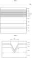
- FIG. 1 is a schematic cross-sectional view illustrating a light emitting diode 100 according to an embodiment of the present disclosure
- FIG. 2 an enlarged schematic cross-sectional view of a portion of FIG. 1 to describe the light emitting diode according to an embodiment of the present disclosure.
- the light emitting diode 100 may include a substrate 10, a buffer layer 20, an undoped layer 30, a first conductivity type semiconductor layer 40, and a pre-strained layer 50, an active region 60, an electron blocking layer 70, and a second conductivity type semiconductor layer 80.
- the substrate 10 may be a growth substrate for growing a gallium nitride-based semiconductor layer, for example, a sapphire substrate, a silicon substrate, a SiC substrate, a spinel substrate, or the like.
- the substrate 10 may be a patterned sapphire substrate.
- the buffer layer 20 may be formed of a low-temperature buffer layer, for example, a nucleation layer such as an AlGaN layer, for growing a gallium nitride-based semiconductor layer on a heterogeneous substrate.
- the undoped layer 30 may be, for example, a high-temperature buffer layer, and include a gallium nitride-based semiconductor layer such as a GaN layer.
- the first conductivity type semiconductor layer 40 may be a semiconductor layer containing an n-type impurity, for example, Si.
- the first conductivity type semiconductor layer 40 may be a contact layer on which an ohmic electrode is formed.
- the pre-strained layer 50 may be disposed between the first conductivity type semiconductor layer 40 and the active region 60.
- the active region 60 includes a high content of In so as to generate light by recombination of electrons and holes. Accordingly, a lattice constant of the active region 60 is greater than that of the first conductivity type semiconductor layer 40, and accordingly, a strain is generated in the active region 60.
- the pre-strained layer 50 refers to a layer formed before the active region 60 in which strain is generated.
- the pre-strained layer 50 may be formed of a single layer or multiple layers.
- the pre-strained layer 50 may include a V-pit generation layer (VGL) for generating V-pits.
- VGL V-pit generation layer
- the VGL may be formed of a single layer of a GaN layer or an InGaN layer or multiple layers including a GaN layer and an InGaN layer, and may be formed at a temperature lower than a growth temperature of the first conductivity type semiconductor layer 40, for example, at a temperature equal to or lower than about 900 °C. By being grown at a relatively low temperature, the VGL may lower densities of threading dislocations and generate V-pits.
- the pre-strained layer 50 may also include an intermediate layer so as to compensate for the strain caused by the active region 60.
- the intermediate layer may be formed of a nitride-based semiconductor layer having a lattice constant smaller than that of the active region 60, and further, may be formed of a nitride-based semiconductor layer having a lattice constant smaller than that of the first conductivity type semiconductor layer 40.
- the intermediate layer may include, for example, an AlN layer and/or an AlGaN layer.
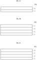
- FIGS. 3A through 3C show various examples 50a, 50b, and 50c of the pre-strained layer 50.
- a pre-strained layer 50a may include a first VGL 5 1 and a second VGL 53.
- both the first VGL 51 and the second VGL 53 may include a GaN layer and/or an InGaN layer.
- the first VGL 51 may be grown at a relatively rapid rate using trimethylgallium (TMGa) as a Ga source
- the second VGL 53 may be grown at a relatively slow rate using triethylgallium (TEGa) as the Ga source.
- TMGa trimethylgallium
- TEGa triethylgallium
- V-pits are generated by the first VGL 51 grown relatively fast at a low temperature, and subsequently, sizes of the V-pits are increased by the second VGL 53.
- the first VGL 51 may be formed of a GaN layer
- the second VGL 53 may be formed of a superlattice layer in which, for example, GaN/InGaN layers are repeatedly stacked.
- An In content of InGaN may be set such that a band gap energy of InGaN is equal to or greater than an energy of light having a wavelength of 405 nm. That is, at least one layer of the first VGL 51 and the second VGL 53 may be formed to have a same composition of a material. Accordingly, in case a lattice change is minimized, it may contribute to generating a white light source with reduced defects.
- a same material used for the first VGL 51 and the second VGL 53 may be a material having an energy band gap larger than that of light generated in the active layer, and may be a material having a lower light absorptivity than that of a well layer of the active layer with respect to light generated in the active layer. Accordingly, light emission efficiency may be increased by preventing absorption of light in an emission path.
- a thickness of the first VGL 51 may be within a range of about 1000 ⁇ to 2500 ⁇ , and a thickness of the second VGL 53 may be within a range of about 1000 ⁇ to 2500 ⁇ . In an embodiment, the thickness of the first VGL 51 may be equal to or greater than that of the second VGL 53. The thickness of the first VGL 51 may be equal to or greater than that of the second VGL 53, and may be less than or equal to three times of the thickness of the second VGL 53. In a particular embodiment, a sum of the thicknesses of the first VGL 51 and the second VGL 53 may be within a range of 250nm to 350nm range. By adjusting the sum of the thicknesses of the first VGL 51 and the second VGL 53 in the range of 250 nm to 350 nm, white light of high luminous intensity may be implemented by a combination of light emitted from the active region 60.
- the first VGL 51 and the second VGL 53 may be doped with an impurity, for example, Si.
- a Si doping concentration doped in the first VGL 51 may be higher than a Si doping concentration doped in the second VGL 51.
- the Si doping concentration doped in the first VGL 51 may be within a range of about 8 ⁇ 10 17 ⁇ 8 ⁇ 10 18 /cm 3
- the Si doping concentration doped in the second VGL 53 may be within a range of about 5 ⁇ 10 17 ⁇ 5 ⁇ 10 18 /cm 3 .
- a pre-strained layer 50b may further include a first intermediate layer 55 and a second intermediate layer 57 in addition to the first and second VGLs 51 and 53 described with reference to FIG. 3A .
- the first intermediate layer 55 and the second intermediate layer 57 may be formed of a nitride-based semiconductor layer having a smaller lattice constant than that of the active region 60, and further, may be formed of a nitride-based semiconductor layer having a smaller lattice constant than that of the first conductivity type semiconductor layer 40.
- the first intermediate layer 55 and the second intermediate layer 57 may have a smaller lattice constant and a wider band gap than those of the first VGL 51 and the second VGL 53.
- One of the first intermediate layer 55 and the second intermediate layer 57 may be an AlN layer, and the other may be an AlGaN layer.
- Average band gap energies of the first intermediate layer 55 and the second intermediate layer 57 disposed over the first VGL 51 and the second VGL 53 may be 0.05 eV or more greater than those of the corresponding first VGL 51 and the second VGL 53, respectively.
- Maximum band gap energies in the first intermediate layer 55 and the second intermediate layer 57 may be 0.12 eV or more greater than those of the corresponding first VGL 51 or the second VGL 53, respectively.
- first intermediate layer 55 and the second intermediate layer 57 having relatively large band gap energies, it is possible to reduce light absorption in the pre-strained layer 50, and accordingly, light extraction efficiency of the light emitting diode may be improved.
- an energy barrier is formed on an interface between the first and second VGLs 51 and 53 and the first and second intermediate layers 55 and 57 due to a difference in band gap, so that a current distribution becomes uniform in the V-pit, and thus, a radiation efficiency of white light can be increased.
- first intermediate layer 55 and the second intermediate layer 57 having a small refractive index are disposed between the active region 60 and the first and second VGLs 51 and 53, so that light may be refracted in a lateral direction, and thus, white light may be effectively emitted in a wide viewing angle range.
- first intermediate layer 55 and the second intermediate layer 57 By disposing the first intermediate layer 55 and the second intermediate layer 57 under the active region 60, a strain caused by the active region 60 may be relieved.
- the first intermediate layer 55 and the second intermediate layer 57 are for relieving the strain generated by the active region 60, and thicknesses thereof may be significantly smaller than those of the first and second VGLs 51 and 53.
- the first intermediate layer 55 and the second intermediate layer 57 may have a thickness within a range of about 10 ⁇ to 150 ⁇ , respectively.
- a pre-strained layer 50c is similar to the pre-strained layer 50b described with reference to FIG. 3B , except that the first intermediate layer 55 and the second intermediate layer 57 are disposed between the first VGL 51 and the second VGL 53.
- first intermediate layer 55 and the second intermediate layer 57 have relatively small thicknesses compared to those of the first and second VGLs 51 and 53, their locations under the active region 60 may be freely changed. At least one of the first and second VGLs 51 and 53 may have a thickness that is 8 times greater than that of at least one of the first intermediate layer 55 and the second intermediate layer 57. Although the first and second intermediate layers 55 and 57 have relatively small lattice constants, a balance of lattice constants on an interface thereof is effectively matched because the first and second VGLs 51 and 53 are relatively thicker.
- a size of the V-pit may be adjusted by the first and second VGLs 51 and 53.
- the size of the V-fit may be increased.
- the size of the V-pit may be defined as a size of a width W of an inlet of the V-pit.
- the V-pit may be completely filled by the second conductivity type semiconductor layer 80, and thus, the width W of the inlet of the V-pit may be defined as a width of an inlet on a surface of the electron blocking layer 70. In a case of the absence of the electron blocking layer 70, the width W may be defined as a width of an inlet on a surface of the active region 60.
- the width of the inlet of the V-pit may be increased in proportion to the thickness of the VGL, for example, the thicknesses of the first and second VGLs 51 and 53. Since the thicknesses of the first and second intermediate layers 55 and 57 are relatively very small, it can be seen that the width of the inlet of the V-pit is increased in proportion to a thickness of the pre-strained layer 50. For example, more than 80% of the V-pits in a 100um ⁇ 100um region may have a width W within a range of ⁇ 10% of the thicknesses of the VGLs 51 and 53 or the thickness of the pre-strained layer 50.
- an angle ⁇ between an inclined surface of the V-pit and a flatness of the pre-strained layer 50 may be within a range of 120° to 150°.
- the light emitting diode 100 may have a high luminous intensity within a specific V-pit size range, and when the V-pit size is smaller than the above range, it is difficult to implement white light, and also when the size thereof is larger than the above range, the luminous intensity is excessively low, thereby making it difficult to use it as a light source.
- a density of the V-pit may be decreased. That is, by adjusting the thicknesses of the VGLs 51 and 53, the density of the V-pit is adjusted. Furthermore, the V-pits formed by the pre-strained layer 50 facilitate to relieve a strain and allow more Indium to be introduced into the active region formed thereon. Accordingly, it is possible to include a multi-quantum well structure containing more Indium in the active region 60 of the light emitting diode 100, and thus, long-wavelength visible light such as red light may be easily implemented, a luminous efficiency of such long-wavelength light may be improved, and furthermore, white light emitting diodes of various colors may be easily manufactured.
- the active region 60 may include a plurality of active layers 60b, 60r, and 60g, and white light may be implemented by mixing lights emitted from these active layers 60b, 60g, and 60r.
- the active layer 60b may have, for example, a multi-quantum well structure emitting blue light within a range of 410 nm to 495 nm
- the active layer 60g may have a multi-quantum well structure emitting green light or yellow light within a range of 520 nm to 605 nm
- the active layer 60r may have a multi-quantum well structure emitting red light within a range of 606 nm to 720 nm.
- the active layers 60b, 60g, and 60r may be formed using a gallium nitride-based semiconductor layer, and may emit light of a desired color according to an In content in the well layer.
- the active region 60 may implement white light by active layers emitting light of two types of colors.
- white light may be implemented by the active layer 60b emitting blue light and the active layer 60g emitting yellow light, or the active layer 60b emitting blue light and the active layer 60r emitting red light.
- Table 1 shows two types of monochromatic complementary wavelengths ( ⁇ 1, ⁇ 2) for implementing white light of 6500K and power ratios required for these wavelengths.
- the active region 60 may be formed along the V-pit, and thus, the V-pit may become larger by the active region 60.
- the electron blocking layer 70 is disposed on the active region 60.
- the electron blocking layer 70 is formed along the surface of the active region 60. As shown in FIG. 2 , the electron blocking layer 70 may be formed along the V-pit formed in the active region 60.
- the second conductivity type semiconductor layer 80 may be disposed on the electron blocking layer70.
- the second conductivity type semiconductor layer 80 may fill the V-pit as shown in FIG. 2 , but the inventive concepts are not limited thereto.
- the second conductivity type semiconductor layer 80 may be formed along the V-pit, and thus, grooves corresponding to the V-pit may remain on a surface of the second conductivity type semiconductor layer 80.
- the second conductivity type semiconductor layer 80 may be a nitride-based semiconductor layer doped with a p-type impurity, for example, Mg.
- the second conductivity type semiconductor layer 80 may include, for example, a GaN layer.
- the second conductivity type semiconductor layer 80 may be a contact layer on which an ohmic electrode is formed.
- CIE color coordinate
- high-efficiency white light may be implemented at a given input current density value by adjusting the size of the V-pit without using the phosphor.
- an intensity of light of a specific color may be easily adjusted.
- active layers emitting blue light may be disposed more than active layers emitting green light. This will be described again later.
- FIG. 4A is a schematic band diagram illustrating a light emitting diode according to an embodiment of the present disclosure.
- a conduction band of a pre-strained layer 50 is shown based on the pre-strained layer 50a of FIG. 3A .
- the first intermediate layer 55 and the second intermediate layer 57 of FIG. 3B and FIG. 3C are not shown separately because their thicknesses are very small.
- Conduction bands of the first intermediate layer 55 and the second intermediate layer 57 may be positioned higher than those of first and second VGLs 51 and 53.
- each of active layers 60b, 60g, and 60r is illustrated as having two well layers for convenience, the inventive concepts are not limited thereto, and may have three or more well layers.
- the pre-strained layer 50 may include a first VGL 51 having a same conduction band as that of a first conductivity type semiconductor layer 40 and a second VGL 53 having a superlattice structure.
- the second VGL 53 may have, for example, a GaN/InGaN superlattice structure.
- the pre-strained layer 50 is disposed between the first conductivity type semiconductor layer 40 and an active region 60.
- the active region 60 includes a plurality of active layers 60b, 60g, and 60r, and these active layers 60b, 60g, and 60r may be disposed such that band gap energies decrease as a distance from the first conductivity type semiconductor layer 40 increases. Since blue light emitted from the active layer 60b has a higher energy than the band gap energies of the active layers 60g and 60r, the light emitting diode according to the illustrated embodiment may be manufactured in a structure in which light generated in the active region 60 is emitted through the first conductivity type semiconductor layer 40.
- FIG. 4B is a schematic band diagram illustrating a light emitting diode according to another embodiment of the present disclosure.
- the light emitting diode according to this embodiment is similar to the light emitting diode described with reference to FIG. 4A , but has a difference in that the active layers 60r, 60g, and 60b are arranged such that the farther the active layers 60r, 60g, and 60b are apart from the first conductivity type semiconductor layer 40, the wider the band gap energies of the active layers 60r, 60g, and 60b are.
- the light emitting diode according to this embodiment may be manufactured in a structure in which light generated in an active region 60 is emitted through a second conductivity type semiconductor layer 80.
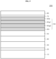
- FIG. 5 is a schematic cross-sectional view illustrating a light emitting diode 200 according to another embodiment of the present disclosure.
- the light emitting diode 200 is substantially similar to the light emitting diode described with reference to FIG. 1 , except that an active region 160 includes active layers 60g1 and 60g2 emitting a plurality of green lights, and locations of active layer 60r emitting red light and active layer 60b emitting blue light are reversed.
- the active layer 60b emitting blue light having a relatively shorter wavelength is disposed closer to a first conductivity type semiconductor layer 40 than the active layer 60r emitting red light having a relatively longer wavelength.
- Light emitted from the active region 160 may be emitted to the outside through the first conductivity type semiconductor layer 40.
- the locations of the active layer 60b emitting blue light and the active layer 60g emitting red light may be reversed depending on a direction in which light is emitted.
- the active layer 60b emitting blue light may be disposed closer to the second conductivity type semiconductor layer 80 than the active layer 60r emitting red light.
- the light emitting diode 200 includes the active layers 60g1 and 60g2 emitting the plurality of green light, a radiation intensity of green light may be increased. Since green light has better luminous efficacy than blue light or red light, visibility of light emitted from the light emitting diode 200 may be improved.
- the active layer 60b may emit light within a wavelength range of 410 nm to 495 nm
- the active layer 60g1 may emit light within a wavelength range of 520 nm to 555 nm
- the active layer 60g2 may emit light within a wavelength range of 560 nm to 605 nm
- the active layer 60r may emit light within a wavelength range of 606 nm to 720 nm.
- FIG. 6 is a schematic cross-sectional view illustrating a light emitting diode 300 according to another embodiment of the present disclosure.
- the light emitting diode 300 is substantially similar to the light emitting diode 200 described with reference to FIG. 5 , except that an active region 260 includes a plurality of active layers 60g1, 60g2, 60g3, and 60g4 emitting green light and a plurality of active layers 60b1, 60b2, and 60b3 emitting blue light.
- three active layers 60b1, 60b2, and 60b3 emitting blue light, four active layers 60g1, 60g2, 60g3, and 60g4 emitting green light, and one active layer 60r emitting red light may be formed.
- the inventive concepts are not limited thereto, and the number of active layers for each color may be adjusted so as to implement white light without using a phosphor.
- the active layers 60b1, 60b2, and 60b3; or 60g1, 60g2, 60g3, and 60g4 emitting light of a same color may emit light having different peak wavelengths, and thus, the light emitting diode 300 may emit four or more colors of polychromatic light.
- the light emitting diode 300 may implement white light having a higher color rendering index than white light implemented by a combination of a single red light, a single green light, and a single blue light.
- a color temperature of white light may be freely adjusted while having the high color rendering index.
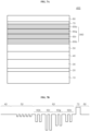
- FIG. 7A is a schematic cross-sectional view illustrating a light emitting diode 400 according to another embodiment of the present disclosure
- FIG. 7B is a schematic band diagram illustrating the light emitting diode 400 of FIG. 7A .
- the light emitting diode 400 is substantially similar to the light emitting diode 100 described with reference to FIG. 1 , except that an active region 360 includes active layers emitting a plurality of blue light, and an active layer 60g emitting green light and an active layer 60r emitting red light are sandwiched between active layers 60b emitting blue light.
- an order of the active layer 60g emitting green light and the active layer 60r emitting red light may be changed.
- the active layers 60b emitting blue light may be disposed in an upper portion and a lower portion of the active region 360.
- the light emitting diode 400 according to this embodiment may emit white light in both directions. That is, the light emitting diode 400 may emit white light not only through a first conductivity type semiconductor layer 40 but also through a second conductivity type semiconductor layer 80.
- FIG. 8 is a schematic partial cross-sectional view illustrating a light emitting diode 500 according to another embodiment of the present disclosure.
- the light emitting diode 500 is substantially similar to the light emitting diode 400 described with reference to FIG. 7A , except that an active region 460 includes a plurality of active layers 60g1, 60g2, 60g3, and 60g4 emitting green light and a plurality of active layers 60b1, 60b2, 60b3, 60b4, 60b5, and 60b6 emitting blue light. Although one active layer 60r emitting red light is illustrated, a plurality of active layers 60r emitting red light may be disposed.
- the plurality of active layers 60b1, 60b2, and 60b3 emitting blue light may be disposed in a lower portion of the active region 460, and the plurality of active layers 60b4, 60b5, and 60b6 emitting blue may be disposed in an upper portion of the active region 460.
- FIG. 9A is a schematic cross-sectional view illustrating a light emitting diode 600 according to another embodiment of the present disclosure
- FIG. 9B is a schematic band diagram illustrating the light emitting diode 600 of FIG. 9A .
- the light emitting diode 600 is substantially similar to the light emitting diode 100 described with reference to FIG. 1 , except that an active region 560 further includes intermediate barrier layers 560a and 560b disposed between active layers 60b, 60g, and 60r.
- the intermediate barrier layer 560a may be disposed between the active layer 60b emitting blue light and the active layer 60g emitting green light, and the intermediate barrier layer 560b may be disposed between the active layer 60g emitting green light and the active layers 60r emitting red light.
- the active region 560 is illustrated and described as including three active layers 60b, 60g, and 60r and two intermediate barrier layers 560a and 560b respectively disposed therebetween, but the inventive concepts are not limited thereto.
- the active region 560 may include two active layers, and in this case, one intermediate barrier layer may be disposed between the active layers.
- the active region 560 includes three active layers 60b, 60g, and 60r, only one intermediate barrier layer 560a or 560b may be disposed between two active layers 60b and 60g, or 60g and 60r.
- the active region 560 may include four or more active layers, and in this case, the intermediate barrier layer may be disposed in at least one of regions between the active layers.
- the intermediate barrier layers 560a and 560b may include a semiconductor layer having a band gap wider than those of the active layers 60b, 60g, and 60r.
- the intermediate barrier layers 560a and 560b may include a nitride-based semiconductor layer containing Al, such as an AlGaN layer, and average band gaps of the intermediate barrier layers 560a and 560b may be wider than band gaps of barrier layers in the active layer 60b, 60g, and 60r.
- the band gaps of the intermediate barrier layers 560a and 560b may be narrower than that of an electron blocking layer 70.
- the intermediate barrier layers 560a and 560b may be formed of multiple layers, as shown in FIG. 9B , or may be formed of a single layer, as shown in FIG. 9C , and a thickness of each of the intermediate barrier layers 560a and 560b may be greater than thicknesses of the barrier layers in the active layers 60b, 60g, and 60r. Furthermore, the intermediate barrier layers 560a and 560b may be doped with an impurity, such as Si.
- the intermediate barrier layers 560a and 560b may control a flow of electrons and holes to increase a luminescent recombination efficiency in the active layers 60b, 60g, and 60r, and may also control an intensity of light emitted from a specific active layer. For example, an injection efficiency of holes may be controlled by adjusting the thicknesses or the band gaps of the intermediate barrier layers 560a and 560b. Accordingly, by adjusting the thicknesses or the band gaps of the intermediate barrier layers 560a and 560b, an intensity ratio of light emitted from the active layers 60b, 60g, and 60r may be adjusted.
- FIG. 10 is a graph showing luminous intensities of light emitting diodes depending on thicknesses of VGLs. All other conditions were same, but only thicknesses of the VGLs 51 and 53 were changed to manufacture the light emitting diodes, and luminous intensities of mixed light emitted from the light emitting diodes depending on the thicknesses of the VGLs 51 and 53 were shown in the graph. V-pits increased in size as the thicknesses of the VGLs 51 and 53 increased. The sizes of the V-pits were roughly comparable to an overall thickness of the VGLs.
- the manufactured light emitting diodes include active layers 60b, 60g, and 60r and intermediate barrier layers 560a and 560b similar to a structure described with reference to FIG.
- first and second VGLs 51 and 53 were manufactured to have a structure described with reference to FIG. 3A .
- an Indium concentration of the second VGL 53 was made to include 3-5%.
- the thicknesses of the first and second VGLs 51 and 53 were made to have a range of ⁇ 20% compared to the size of the V-pit.
- the light emitting diode when the thickness of the VGL was about 300 nm, the light emitting diode exhibited white light and exhibited a highest luminous intensity.
- the thickness of the VGL is proportional to the size of the V-pit. To implement light with the high luminous intensity, it is necessary to adjust the size of the V-pit within a specific range. At least 80% of the V-pits may be formed to have a size within a range of about 250 nm to about 350 nm. Accordingly, it is possible to provide a light emitting diode that emits white light with the high luminous intensity.
- pre-strained layers 50a, 50b, and 50c described with reference to FIGS. 3A through 3C may be applied to the pre-strained layers 50 of FIGS. 5 , 6 , 7A , 8 , and 9A , respectively.
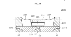
- FIG. 11 is a schematic cross-sectional view illustrating a light emitting device 2000 according to an embodiment of the present disclosure.
- the light emitting device 2000 may include a first lead 221a, a second lead 221b, a housing 223, light emitting diode chips 225, a reflector 227, an adhesive 229, and a wavelength converter 231.
- the first lead 221a and the second lead 221b may be formed of a conductive material, for example, a metal. Bottom surfaces of the first lead 221a and the second lead 221b may be partially removed by half-cutting, and thus, may include relatively thin regions. In addition, the first lead 221a and the second lead 221b may be separated from each other by etching. Furthermore, although not shown in the drawing, a through-hole may be formed in each of the first lead 221a and the second lead 221b. The through-hole may be connected to the region in which the bottom surface is partially removed. The through-holes are filled with the housing 223, thereby preventing the leads 221a and 221b from being separated from the housing 223. The through-hole is selectively applicable.
- the leads 221a and 221b may have surfaces facing each other.
- the surfaces of the leads 221a and 221b facing each other may be symmetrical.
- the surface of each of the leads 221a and 221b facing each other may include a first surface s1 and a second surface s2.
- the first surface s1 may include a region having a first radius of curvature
- the second surface s2 may include a region having a second radius of curvature.
- the first radius of curvature may have a value different from that of the second radius of curvature. As shown in FIG. 20, the first radius of curvature of the first surface s1 may be smaller than the second radius of curvature of the second surface s2.
- first and second leads 221a and 221b may include curved surfaces, that is, a third surface s3, and a fourth surface s4, along with vertical surfaces on opposite side surfaces of each other.
- the opposite side surfaces may be symmetrical, but the inventive concepts are not limited thereto.
- the third and fourth surfaces s3 and s4 may include a region having different radii of curvature from those of the first and second surfaces s1 and s2.
- the third surface s3 and the fourth surface s4 may include a region having the radius of curvature greater than those of the first surface s1 and the second surface s2.
- a coupling force between the leads 221a and 221b and the housing 223 may be enhanced.
- the housing 223 covers portions of upper surfaces of the leads 221a and 221b and portions of lower surfaces of the leads 221a and 221b.
- the housing 223 may fill the region in which the bottom surface is partially removed by half-cutting, and may fill the through-holes formed in the leads 221a and 221b.
- the housing 223 forms a cavity over the leads 221a and 221b.
- the housing 223 may be formed of, for example, an epoxy molding compound (EMC).
- EMC epoxy molding compound
- the light emitting diode chip 225 may be electrically connected by flip bonding or wire connection on the first lead 221a and the second lead 221b.
- the light emitting diode chip 225 may include the light emitting diodes described in the previous embodiments.
- a first material layer 231 is disposed over the light emitting diode chip 225.
- the first material layer 231 may be adhered to the light emitting diode chip 225 through the adhesive 229 or may be disposed as a molding.
- the adhesive 229 may at least partially cover an upper surface as well as side surfaces of the light emitting diode chip 225.
- a thickness of the adhesive 229 covering the side surfaces of the light emitting diode chip 225 may be decreased toward a lower surface of the light emitting diode chip 225.
- the first material layer 231 may be formed of a light-transmitting material such that light passes as it is without wavelength conversion, or may include a phosphor to convert a wavelength of light so as to implement a desired color coordinate.
- a light-transmitting material such that light passes as it is without wavelength conversion
- a phosphor to convert a wavelength of light so as to implement a desired color coordinate.
- an amount of phosphor used may be relatively less than that of a conventional light emitting device. By using the phosphor together with the light emitting diode chip 225 emitting mixed light, mixed light having a desired color coordinate may be easily implemented.
- a second material layer 227 may be formed between an inner wall of the housing 223 and the wavelength converter 231.
- the second material layer 227 may contact a side surface of the first material layer 231 and may contact the inner wall of the housing 223.
- the second material layer 227 may also surround the side surfaces of the light emitting diode chip 225.
- the adhesive 229 may be disposed between the second material layer 227 and the light emitting diode chip 225.
- the second material layer 227 When the second material layer 227 is formed of a reflective material, it may be formed of a material having a higher reflectance than that of the housing 223, and the reflector 227 may include regions having different heights in cross-section view. For example, it may include white silicone.
- the second material layer 227 may include a concave upper surface. A lowest height of a concave portion may be disposed lower than an upper surface (indicated by a dotted line) of the first material layer 231, and an uppermost end of the second material layer 227 may be disposed higher than the upper surface of the first material layer 231. Accordingly, light emitted in a lateral direction from the first material layer 231 may be reflected from the concave upper surface of the second material layer 227, and thus, light may be collected in an upper direction of the light emitting diode chip 225.
- the inventive concepts are not necessarily limited thereto, and the first material layer 231 and the second material layer 227 may be formed of a same material and formed in one shape.
- one material layer may cover the side surfaces and the upper surface of the light emitting diode chip 225 and may fill an interior of a cavity of the housing 223.
- the light emitting device 2000 may easily implement mixed color light having a desired color coordinate by using the phosphor together with the light emitting diode chip 225 emitting mixed color light.
Landscapes
- Led Devices (AREA)
Abstract
Description
- The present disclosure relates to a light emitting diode, and more particularly, to a light emitting diode for implementing white light.
- Nitride semiconductors are used as light sources for displaying apparatuses, traffic lights, lighting, or optical communication devices, and may be mainly used for light emitting diodes or laser diodes that emit blue or green light. In addition, the nitride semiconductors may be used in a heterojunction bipolar transistor (HBT), a high electron mobility transistor (HEMT), and the like.
- In general, a light emitting diode using the nitride semiconductor has a heterojunction structure having a quantum well structure between an N contact layer and a P contact layer. The light emitting diode emits light of a specific wavelength depending on a composition of a well layer in the quantum well structure. To increase internal quantum efficiency and reduce losses due to light absorption, the light emitting diode is designed to emit a spectrum of light having a single peak, i.e. monochromatic light.
- However, mixed color light emitted from lighting or the like, for example, white light is difficult to implement with a single peak monochromatic light. Accordingly, a technique of implementing white light by using a plurality of light emitting diodes together emitting different monochromatic light from one another or by using a phosphor converting a wavelength of light emitted from the light emitting diode is generally used.
- The use of phosphors comes with cost of phosphor or a decrease in efficiency known as a Stoke's shift. In addition, a process of coating phosphor on the light emitting diode and yellowing of a carrier carrying phosphor should also be considered.
- Using a mixture of a plurality of light emitting diodes complicates the process, and it is inconvenient to prepare light emitting diodes made of different materials.
- When light having a spectrum of multi-bands is implemented using a single-chip light emitting diode, many drawbacks caused by using the plurality of light emitting diodes or using the phosphor can be avoided.
- A conventional white light has been implemented through, for example, an LED package that combines a blue LED and a phosphor. However, when a package structure including the LED and the phosphor layer is applied to various applications, there is a space limitation. For design freedom of an LED device, it is necessary to simplify a structure of a light source as much as possible, and it is necessary to prevent reduction of radiation efficiency due to deterioration of the phosphor.
- Embodiments of the present disclosure provide a light emitting diode suitable for implementing mixed color light, for example, white light without using a phosphor.
- A light emitting diode according to an embodiment of the present disclosure includes a first conductivity type semiconductor layer; an active region including a plurality of active layers; a pre-strained layer disposed between the first conductivity type semiconductor layer and the active region, and including a V-pit generation layer (VGL); and a second conductivity type semiconductor layer disposed on the active region, in which the VGL has a thickness within a range of 250 nm to 350 nm.
- The active region may emit white light having a plurality of peak wavelengths.
- The VGL may include a first VGL and a second VGL.
- The first VGL may be a single layer, and the second VGL may be a superlattice layer.
- The superlattice layer may include an InGaN layer, and a band gap energy of the InGaN layer may be equal to or greater than an energy of light of 405 nm.
- The first VGL may be a layer formed using TMGa as a Ga source, and the second VGL may be formed using TEGa as the Ga source.
- The pre-strained layer may further include a first intermediate layer and a second intermediate layer, and the first and second intermediate layers may be nitride-based semiconductor layers having a lattice constant smaller than that of the active region.
- One of the first and second intermediate layers may be an AlN layer, and the other may be an AlGaN layer.
- The first intermediate layer and the second intermediate layer may be disposed between the first VGL and the second VGL.
- The first and second VGLs may have a thickness within a range of 1000 Å to 2500Å, respectively, and the first and second intermediate layers may have a thickness within a range of 10 Å to 150 Å, respectively.
- The active region may include at least one active layer emitting blue light, at least one active layer emitting green light, and at least one active layer emitting red light, in which the blue light has a peak wavelength within a range of 410 nm to 495 nm, the green light has a peak wavelength within a range of 520 nm to 605 nm, and the red light has a peak wavelength within a range of 606 nm to 720 nm.
- The active layers emitting green light and red light may be disposed between the active layers emitting blue light.
- The active region may further include an intermediate barrier layer disposed between the active layers, in which the intermediate barrier layer may have a wider energy band gap than those of barrier layers in the active layers.
- The intermediate barrier layer may be formed of a single layer or in multiple layers.
- The light emitting diode may further include an electron blocking layer, and the intermediate barrier layer may have a narrower energy band gap than that of the electron blocking layer.
- The active region may include at least three active layers, and the intermediate barrier layer may be disposed in at least one of regions between the active layers.
- A light emitting diode according to an embodiment of the present disclosure includes a first conductivity type semiconductor layer; an active region including a plurality of active layers; a pre-strained layer disposed between the first conductivity type semiconductor layer and the active region, and including a V-pit generation layer; and a second conductivity type semiconductor layer disposed on the active region, in which the pre-strained layer includes a first VGL, a second VGL, a first intermediate layer, and a second intermediate layer, in which the first intermediate layer and the second intermediate layer have a lattice constant greater than that of the active region.
- The active region may emit white light having a plurality of peak wavelengths.
- The first VGL may be a GaN layer, and the second VGL may be a GaN/InGaN superlattice layer. One of the first intermediate layer and the second intermediate layer may be an AlN layer, and the other may be an AlGaN layer.
- The first intermediate layer and the second intermediate layer may be disposed between the first VGL and the second VGL.
-
-
FIG. 1 is a schematic cross-sectional view illustrating a light emitting diode according to an embodiment of the present disclosure. -
FIG. 2 is an enlarged schematic cross-sectional view of a portion ofFIG. 1 to describe the light emitting diode according to an embodiment of the present disclosure. -
FIG. 3A is a schematic partial cross-sectional view illustrating a light emitting diode according to an embodiment of the present disclosure. -
FIG. 3B is a schematic partial cross-sectional view illustrating a light emitting diode according to another embodiment of the present disclosure. -
FIG. 3C is a schematic partial cross-sectional view illustrating a light emitting diode according to another embodiment of the present disclosure. -
FIG. 4A is a schematic band diagram illustrating a light emitting diode according to an embodiment of the present disclosure. -
FIG. 4B is a schematic band diagram illustrating a light emitting diode according to another embodiment of the present disclosure. -
FIG. 5 is a schematic cross-sectional view illustrating a light emitting diode according to another embodiment of the present disclosure. -
FIG. 6 is a schematic cross-sectional view illustrating a light emitting diode according to another embodiment of the present disclosure. -
FIG. 7A is a schematic cross-sectional view illustrating a light emitting diode according to another embodiment of the present disclosure. -
FIG. 7B is a schematic band diagram illustrating the light emitting diode ofFIG. 7A . -
FIG. 8 is a schematic cross-sectional view illustrating a light emitting diode according to another embodiment of the present disclosure. -
FIG. 9A is a schematic cross-sectional view illustrating a light emitting diode according to another embodiment of the present disclosure. -
FIG. 9B is a schematic band diagram illustrating the light emitting diode ofFIG. 9A . -
FIG. 9C is a schematic band diagram illustrating the light emitting diode ofFIG. 9A . -
FIG. 10 is a graph showing luminous intensities depending on thicknesses of VGLs. -
FIG. 11 is a schematic cross-sectional view illustrating a light emitting device according to an embodiment of the present disclosure. - Hereinafter, exemplary embodiments of the present disclosure will be described in detail with reference to the accompanying drawings. The following embodiments are provided by way of example so as to fully convey the spirit of the present disclosure to those skilled in the art to which the present disclosure pertains. Accordingly, the present disclosure is not limited to the exemplary embodiments disclosed herein and can also be implemented in different forms. In the drawings, widths, lengths, thicknesses, and the like of elements can be exaggerated for clarity and descriptive purposes. When an element or layer is referred to as being "disposed above" or "disposed on" another element or layer, it can be directly "disposed above" or "disposed on" the other element or layer or intervening elements or layers can be present. Throughout the specification, like reference numerals denote like elements having the same or similar functions.
-
FIG. 1 is a schematic cross-sectional view illustrating alight emitting diode 100 according to an embodiment of the present disclosure, andFIG. 2 an enlarged schematic cross-sectional view of a portion ofFIG. 1 to describe the light emitting diode according to an embodiment of the present disclosure. - Referring to
FIG. 1 , thelight emitting diode 100 may include asubstrate 10, abuffer layer 20, anundoped layer 30, a first conductivitytype semiconductor layer 40, and apre-strained layer 50, anactive region 60, anelectron blocking layer 70, and a second conductivitytype semiconductor layer 80. - The
substrate 10 may be a growth substrate for growing a gallium nitride-based semiconductor layer, for example, a sapphire substrate, a silicon substrate, a SiC substrate, a spinel substrate, or the like. In an embodiment, thesubstrate 10 may be a patterned sapphire substrate. - The
buffer layer 20 may be formed of a low-temperature buffer layer, for example, a nucleation layer such as an AlGaN layer, for growing a gallium nitride-based semiconductor layer on a heterogeneous substrate. Theundoped layer 30 may be, for example, a high-temperature buffer layer, and include a gallium nitride-based semiconductor layer such as a GaN layer. - The first conductivity
type semiconductor layer 40 may be a semiconductor layer containing an n-type impurity, for example, Si. The first conductivitytype semiconductor layer 40 may be a contact layer on which an ohmic electrode is formed. - The
pre-strained layer 50 may be disposed between the first conductivitytype semiconductor layer 40 and theactive region 60. Theactive region 60 includes a high content of In so as to generate light by recombination of electrons and holes. Accordingly, a lattice constant of theactive region 60 is greater than that of the first conductivitytype semiconductor layer 40, and accordingly, a strain is generated in theactive region 60. Thepre-strained layer 50 refers to a layer formed before theactive region 60 in which strain is generated. - The
pre-strained layer 50 may be formed of a single layer or multiple layers. Thepre-strained layer 50 may include a V-pit generation layer (VGL) for generating V-pits. The VGL may be formed of a single layer of a GaN layer or an InGaN layer or multiple layers including a GaN layer and an InGaN layer, and may be formed at a temperature lower than a growth temperature of the first conductivitytype semiconductor layer 40, for example, at a temperature equal to or lower than about 900 °C. By being grown at a relatively low temperature, the VGL may lower densities of threading dislocations and generate V-pits. Thepre-strained layer 50 may also include an intermediate layer so as to compensate for the strain caused by theactive region 60. The intermediate layer may be formed of a nitride-based semiconductor layer having a lattice constant smaller than that of theactive region 60, and further, may be formed of a nitride-based semiconductor layer having a lattice constant smaller than that of the first conductivitytype semiconductor layer 40. The intermediate layer may include, for example, an AlN layer and/or an AlGaN layer. -
FIGS. 3A through 3C show various examples 50a, 50b, and 50c of thepre-strained layer 50. - Referring to
FIG. 3A , apre-strained layer 50a may include a first VGL 5 1 and asecond VGL 53. For example, both thefirst VGL 51 and thesecond VGL 53 may include a GaN layer and/or an InGaN layer. Thefirst VGL 51 may be grown at a relatively rapid rate using trimethylgallium (TMGa) as a Ga source, and thesecond VGL 53 may be grown at a relatively slow rate using triethylgallium (TEGa) as the Ga source. V-pits are generated by thefirst VGL 51 grown relatively fast at a low temperature, and subsequently, sizes of the V-pits are increased by thesecond VGL 53. By growing thesecond VGL 53 using the TEGa source on thefirst VGL 51, V-pits of relatively uniform densities and sizes may be formed over an entire wafer area. - For example, the
first VGL 51 may be formed of a GaN layer, and thesecond VGL 53 may be formed of a superlattice layer in which, for example, GaN/InGaN layers are repeatedly stacked. An In content of InGaN may be set such that a band gap energy of InGaN is equal to or greater than an energy of light having a wavelength of 405 nm. That is, at least one layer of thefirst VGL 51 and thesecond VGL 53 may be formed to have a same composition of a material. Accordingly, in case a lattice change is minimized, it may contribute to generating a white light source with reduced defects. - A same material used for the
first VGL 51 and thesecond VGL 53 may be a material having an energy band gap larger than that of light generated in the active layer, and may be a material having a lower light absorptivity than that of a well layer of the active layer with respect to light generated in the active layer. Accordingly, light emission efficiency may be increased by preventing absorption of light in an emission path. - A thickness of the
first VGL 51 may be within a range of about 1000 Å to 2500 Å, and a thickness of thesecond VGL 53 may be within a range of about 1000 Å to 2500 Å. In an embodiment, the thickness of thefirst VGL 51 may be equal to or greater than that of thesecond VGL 53. The thickness of thefirst VGL 51 may be equal to or greater than that of thesecond VGL 53, and may be less than or equal to three times of the thickness of thesecond VGL 53. In a particular embodiment, a sum of the thicknesses of thefirst VGL 51 and thesecond VGL 53 may be within a range of 250nm to 350nm range. By adjusting the sum of the thicknesses of thefirst VGL 51 and thesecond VGL 53 in the range of 250 nm to 350 nm, white light of high luminous intensity may be implemented by a combination of light emitted from theactive region 60. - Meanwhile, the
first VGL 51 and thesecond VGL 53 may be doped with an impurity, for example, Si. A Si doping concentration doped in thefirst VGL 51 may be higher than a Si doping concentration doped in thesecond VGL 51. For example, the Si doping concentration doped in thefirst VGL 51 may be within a range of about 8×10¹⁷~8×10¹⁸/cm3, and the Si doping concentration doped in thesecond VGL 53 may be within a range of about 5×10¹⁷~5×10¹⁸/cm3. - Referring to
FIG. 3B , apre-strained layer 50b may further include a firstintermediate layer 55 and a secondintermediate layer 57 in addition to the first and second VGLs 51 and 53 described with reference toFIG. 3A . The firstintermediate layer 55 and the secondintermediate layer 57 may be formed of a nitride-based semiconductor layer having a smaller lattice constant than that of theactive region 60, and further, may be formed of a nitride-based semiconductor layer having a smaller lattice constant than that of the first conductivitytype semiconductor layer 40. The firstintermediate layer 55 and the secondintermediate layer 57 may have a smaller lattice constant and a wider band gap than those of thefirst VGL 51 and thesecond VGL 53. One of the firstintermediate layer 55 and the secondintermediate layer 57 may be an AlN layer, and the other may be an AlGaN layer. Average band gap energies of the firstintermediate layer 55 and the secondintermediate layer 57 disposed over thefirst VGL 51 and thesecond VGL 53 may be 0.05 eV or more greater than those of the correspondingfirst VGL 51 and thesecond VGL 53, respectively. Maximum band gap energies in the firstintermediate layer 55 and the secondintermediate layer 57 may be 0.12 eV or more greater than those of the correspondingfirst VGL 51 or thesecond VGL 53, respectively. By disposing the firstintermediate layer 55 and the secondintermediate layer 57 having relatively large band gap energies, it is possible to reduce light absorption in thepre-strained layer 50, and accordingly, light extraction efficiency of the light emitting diode may be improved. In addition, an energy barrier is formed on an interface between the first and second VGLs 51 and 53 and the first and secondintermediate layers - In addition, the first
intermediate layer 55 and the secondintermediate layer 57 having a small refractive index are disposed between theactive region 60 and the first and second VGLs 51 and 53, so that light may be refracted in a lateral direction, and thus, white light may be effectively emitted in a wide viewing angle range. - By disposing the first
intermediate layer 55 and the secondintermediate layer 57 under theactive region 60, a strain caused by theactive region 60 may be relieved. The firstintermediate layer 55 and the secondintermediate layer 57 are for relieving the strain generated by theactive region 60, and thicknesses thereof may be significantly smaller than those of the first and second VGLs 51 and 53. For example, the firstintermediate layer 55 and the secondintermediate layer 57 may have a thickness within a range of about 10 Å to 150 Å, respectively. - Referring to
FIG. 3C , apre-strained layer 50c is similar to thepre-strained layer 50b described with reference toFIG. 3B , except that the firstintermediate layer 55 and the secondintermediate layer 57 are disposed between thefirst VGL 51 and thesecond VGL 53. - Since the first
intermediate layer 55 and the secondintermediate layer 57 have relatively small thicknesses compared to those of the first and second VGLs 51 and 53, their locations under theactive region 60 may be freely changed. At least one of the first and second VGLs 51 and 53 may have a thickness that is 8 times greater than that of at least one of the firstintermediate layer 55 and the secondintermediate layer 57. Although the first and secondintermediate layers - A size of the V-pit may be adjusted by the first and second VGLs 51 and 53. When the thicknesses of the first and second VGLs 51 and 53 are increased, the size of the V-fit may be increased. As shown in
FIG. 2 , the size of the V-pit may be defined as a size of a width W of an inlet of the V-pit. The V-pit may be completely filled by the second conductivitytype semiconductor layer 80, and thus, the width W of the inlet of the V-pit may be defined as a width of an inlet on a surface of theelectron blocking layer 70. In a case of the absence of theelectron blocking layer 70, the width W may be defined as a width of an inlet on a surface of theactive region 60. - The width of the inlet of the V-pit may be increased in proportion to the thickness of the VGL, for example, the thicknesses of the first and second VGLs 51 and 53. Since the thicknesses of the first and second
intermediate layers pre-strained layer 50. For example, more than 80% of the V-pits in a 100um×100um region may have a width W within a range of ±10% of the thicknesses of theVGLs pre-strained layer 50. In addition, an angle Θ between an inclined surface of the V-pit and a flatness of thepre-strained layer 50 may be within a range of 120° to 150°. As it will be described later, thelight emitting diode 100 may have a high luminous intensity within a specific V-pit size range, and when the V-pit size is smaller than the above range, it is difficult to implement white light, and also when the size thereof is larger than the above range, the luminous intensity is excessively low, thereby making it difficult to use it as a light source. - Meanwhile, as the size of the V-pit is increased, a density of the V-pit may be decreased. That is, by adjusting the thicknesses of the
VGLs pre-strained layer 50 facilitate to relieve a strain and allow more Indium to be introduced into the active region formed thereon. Accordingly, it is possible to include a multi-quantum well structure containing more Indium in theactive region 60 of thelight emitting diode 100, and thus, long-wavelength visible light such as red light may be easily implemented, a luminous efficiency of such long-wavelength light may be improved, and furthermore, white light emitting diodes of various colors may be easily manufactured. - Referring back to
FIG. 1 , theactive region 60 may include a plurality ofactive layers active layers active layer 60b may have, for example, a multi-quantum well structure emitting blue light within a range of 410 nm to 495 nm, theactive layer 60g may have a multi-quantum well structure emitting green light or yellow light within a range of 520 nm to 605 nm, and theactive layer 60r may have a multi-quantum well structure emitting red light within a range of 606 nm to 720 nm. Theactive layers - Although the
active region 60 is illustrated and described as including theactive layers active region 60 may implement white light by active layers emitting light of two types of colors. For example, white light may be implemented by theactive layer 60b emitting blue light and theactive layer 60g emitting yellow light, or theactive layer 60b emitting blue light and theactive layer 60r emitting red light. Table 1 shows two types of monochromatic complementary wavelengths (λ1, λ2) for implementing white light of 6500K and power ratios required for these wavelengths.[Table 1] Complementary Color Luminous Intensity Ratio λ1(nm) λ2(nm) P(λ2)/P(λ1) 380~400 540~570 0.000642~0.0785 400~420 540~570 0.0785~0.89 420~430 540~570 0.89~1.42 430~450 540~570 1.42~1.79 450~470 540~570 1.79~1.09 470~480 570~600 1.09~0.81 480∼490 600∼630 0.81∼0.668 - As shown in
FIG. 2 , theactive region 60 may be formed along the V-pit, and thus, the V-pit may become larger by theactive region 60. - The
electron blocking layer 70 is disposed on theactive region 60. Theelectron blocking layer 70 is formed along the surface of theactive region 60. As shown inFIG. 2 , theelectron blocking layer 70 may be formed along the V-pit formed in theactive region 60. - The second conductivity
type semiconductor layer 80 may be disposed on the electron blocking layer70. The second conductivitytype semiconductor layer 80 may fill the V-pit as shown inFIG. 2 , but the inventive concepts are not limited thereto. For example, the second conductivitytype semiconductor layer 80 may be formed along the V-pit, and thus, grooves corresponding to the V-pit may remain on a surface of the second conductivitytype semiconductor layer 80. - The second conductivity
type semiconductor layer 80 may be a nitride-based semiconductor layer doped with a p-type impurity, for example, Mg. The second conductivitytype semiconductor layer 80 may include, for example, a GaN layer. The second conductivitytype semiconductor layer 80 may be a contact layer on which an ohmic electrode is formed. - According to the illustrated embodiment, by using the
active region 60 having the plurality ofactive layers light emitting diode 100 according to the illustrated embodiment, high-efficiency white light may be implemented at a given input current density value by adjusting the size of the V-pit without using the phosphor. - Moreover, in case light of a desired color is emitted using the
active layers -
FIG. 4A is a schematic band diagram illustrating a light emitting diode according to an embodiment of the present disclosure. Here, only conduction bands are shown, and valence bands are omitted. In addition, a conduction band of apre-strained layer 50 is shown based on thepre-strained layer 50a ofFIG. 3A . The firstintermediate layer 55 and the secondintermediate layer 57 ofFIG. 3B and FIG. 3C are not shown separately because their thicknesses are very small. Conduction bands of the firstintermediate layer 55 and the secondintermediate layer 57 may be positioned higher than those of first and second VGLs 51 and 53. Meanwhile, although each ofactive layers - Referring to
FIG. 4A , as described with reference toFIG. 3A , thepre-strained layer 50 may include afirst VGL 51 having a same conduction band as that of a first conductivitytype semiconductor layer 40 and asecond VGL 53 having a superlattice structure. Thesecond VGL 53 may have, for example, a GaN/InGaN superlattice structure. Thepre-strained layer 50 is disposed between the first conductivitytype semiconductor layer 40 and anactive region 60. - Meanwhile, the
active region 60 includes a plurality ofactive layers active layers type semiconductor layer 40 increases. Since blue light emitted from theactive layer 60b has a higher energy than the band gap energies of theactive layers active region 60 is emitted through the first conductivitytype semiconductor layer 40. -
FIG. 4B is a schematic band diagram illustrating a light emitting diode according to another embodiment of the present disclosure. The light emitting diode according to this embodiment is similar to the light emitting diode described with reference toFIG. 4A , but has a difference in that theactive layers active layers type semiconductor layer 40, the wider the band gap energies of theactive layers - According to this embodiment, since blue light emitted from the
active layer 60b has a higher energy than band gap energies of theactive layers active region 60 is emitted through a second conductivitytype semiconductor layer 80. -
FIG. 5 is a schematic cross-sectional view illustrating alight emitting diode 200 according to another embodiment of the present disclosure. - Referring to
FIG. 5 , thelight emitting diode 200 according to this embodiment is substantially similar to the light emitting diode described with reference toFIG. 1 , except that anactive region 160 includes active layers 60g1 and 60g2 emitting a plurality of green lights, and locations ofactive layer 60r emitting red light andactive layer 60b emitting blue light are reversed. - In this embodiment, the
active layer 60b emitting blue light having a relatively shorter wavelength is disposed closer to a first conductivitytype semiconductor layer 40 than theactive layer 60r emitting red light having a relatively longer wavelength. Light emitted from theactive region 160 may be emitted to the outside through the first conductivitytype semiconductor layer 40. - As previously described with reference to
FIG. 4A and FIG. 4B , the locations of theactive layer 60b emitting blue light and theactive layer 60g emitting red light may be reversed depending on a direction in which light is emitted. For example, to emit light to the outside through a second conductivitytype semiconductor layer 80, theactive layer 60b emitting blue light may be disposed closer to the second conductivitytype semiconductor layer 80 than theactive layer 60r emitting red light. - Meanwhile, in this embodiment, in case the
light emitting diode 200 includes the active layers 60g1 and 60g2 emitting the plurality of green light, a radiation intensity of green light may be increased. Since green light has better luminous efficacy than blue light or red light, visibility of light emitted from thelight emitting diode 200 may be improved. - For example, the
active layer 60b may emit light within a wavelength range of 410 nm to 495 nm, the active layer 60g1 may emit light within a wavelength range of 520 nm to 555 nm, the active layer 60g2 may emit light within a wavelength range of 560 nm to 605 nm, and theactive layer 60r may emit light within a wavelength range of 606 nm to 720 nm. -
FIG. 6 is a schematic cross-sectional view illustrating alight emitting diode 300 according to another embodiment of the present disclosure. - Referring to
Figure 6 , thelight emitting diode 300 according to this embodiment is substantially similar to thelight emitting diode 200 described with reference toFIG. 5 , except that anactive region 260 includes a plurality of active layers 60g1, 60g2, 60g3, and 60g4 emitting green light and a plurality of active layers 60b1, 60b2, and 60b3 emitting blue light. - In this embodiment, three active layers 60b1, 60b2, and 60b3 emitting blue light, four active layers 60g1, 60g2, 60g3, and 60g4 emitting green light, and one
active layer 60r emitting red light may be formed. However, the inventive concepts are not limited thereto, and the number of active layers for each color may be adjusted so as to implement white light without using a phosphor. - The active layers 60b1, 60b2, and 60b3; or 60g1, 60g2, 60g3, and 60g4 emitting light of a same color may emit light having different peak wavelengths, and thus, the
light emitting diode 300 may emit four or more colors of polychromatic light. By emitting light having various peak wavelengths, thelight emitting diode 300 may implement white light having a higher color rendering index than white light implemented by a combination of a single red light, a single green light, and a single blue light. In addition, since light having various wavelengths can be selected, a color temperature of white light may be freely adjusted while having the high color rendering index. -
FIG. 7A is a schematic cross-sectional view illustrating alight emitting diode 400 according to another embodiment of the present disclosure, andFIG. 7B is a schematic band diagram illustrating thelight emitting diode 400 ofFIG. 7A . - Referring to
FIGS. 7A and 7B , thelight emitting diode 400 according to this embodiment is substantially similar to thelight emitting diode 100 described with reference toFIG. 1 , except that anactive region 360 includes active layers emitting a plurality of blue light, and anactive layer 60g emitting green light and anactive layer 60r emitting red light are sandwiched betweenactive layers 60b emitting blue light. In addition, an order of theactive layer 60g emitting green light and theactive layer 60r emitting red light may be changed. - The
active layers 60b emitting blue light may be disposed in an upper portion and a lower portion of theactive region 360. Thelight emitting diode 400 according to this embodiment may emit white light in both directions. That is, thelight emitting diode 400 may emit white light not only through a first conductivitytype semiconductor layer 40 but also through a second conductivitytype semiconductor layer 80. -
FIG. 8 is a schematic partial cross-sectional view illustrating alight emitting diode 500 according to another embodiment of the present disclosure. - Referring to
FIG. 8 , thelight emitting diode 500 according to this embodiment is substantially similar to thelight emitting diode 400 described with reference toFIG. 7A , except that an active region 460 includes a plurality of active layers 60g1, 60g2, 60g3, and 60g4 emitting green light and a plurality of active layers 60b1, 60b2, 60b3, 60b4, 60b5, and 60b6 emitting blue light. Although oneactive layer 60r emitting red light is illustrated, a plurality ofactive layers 60r emitting red light may be disposed. In addition, the plurality of active layers 60b1, 60b2, and 60b3 emitting blue light may be disposed in a lower portion of the active region 460, and the plurality of active layers 60b4, 60b5, and 60b6 emitting blue may be disposed in an upper portion of the active region 460. -
FIG. 9A is a schematic cross-sectional view illustrating alight emitting diode 600 according to another embodiment of the present disclosure, andFIG. 9B is a schematic band diagram illustrating thelight emitting diode 600 ofFIG. 9A . - Referring to
FIG. 9A and FIG. 9B , thelight emitting diode 600 according to this embodiment is substantially similar to thelight emitting diode 100 described with reference toFIG. 1 , except that anactive region 560 further includesintermediate barrier layers active layers - The
intermediate barrier layer 560a may be disposed between theactive layer 60b emitting blue light and theactive layer 60g emitting green light, and theintermediate barrier layer 560b may be disposed between theactive layer 60g emitting green light and theactive layers 60r emitting red light. In this embodiment, theactive region 560 is illustrated and described as including threeactive layers intermediate barrier layers active region 560 may include two active layers, and in this case, one intermediate barrier layer may be disposed between the active layers. In addition, although theactive region 560 includes threeactive layers intermediate barrier layer active layers active region 560 may include four or more active layers, and in this case, the intermediate barrier layer may be disposed in at least one of regions between the active layers. - The
intermediate barrier layers active layers intermediate barrier layers intermediate barrier layers active layer intermediate barrier layers electron blocking layer 70. - The
intermediate barrier layers FIG. 9B , or may be formed of a single layer, as shown inFIG. 9C , and a thickness of each of theintermediate barrier layers active layers intermediate barrier layers - The
intermediate barrier layers active layers intermediate barrier layers intermediate barrier layers active layers -
FIG. 10 is a graph showing luminous intensities of light emitting diodes depending on thicknesses of VGLs. All other conditions were same, but only thicknesses of theVGLs VGLs VGLs active layers intermediate barrier layers FIG. 9A , and also first and second VGLs 51 and 53 were manufactured to have a structure described with reference toFIG. 3A . In the above case, an Indium concentration of thesecond VGL 53 was made to include 3-5%. In addition, the thicknesses of the first and second VGLs 51 and 53 were made to have a range of ±20% compared to the size of the V-pit. - Referring to
FIG. 10 , when the thickness of the VGL was about 300 nm, the light emitting diode exhibited white light and exhibited a highest luminous intensity. A light emitting diode having a VGL thickness of about 200 nm emitted green light instead of white light, and in a case of about 500 nm of the thickness, blue light was emitted. A light emitting diode having a VGL thickness of about 400 nm emitted white light, but had a relatively low luminous intensity. - The thickness of the VGL is proportional to the size of the V-pit. To implement light with the high luminous intensity, it is necessary to adjust the size of the V-pit within a specific range. At least 80% of the V-pits may be formed to have a size within a range of about 250 nm to about 350 nm. Accordingly, it is possible to provide a light emitting diode that emits white light with the high luminous intensity.
- Various embodiments have been described above, and the matters described in one embodiment may be applied to other embodiments without departing from the spirit of the present disclosure. For example, the
pre-strained layers FIGS. 3A through 3C may be applied to thepre-strained layers 50 ofFIGS. 5 ,6 ,7A ,8 , and9A , respectively. -
FIG. 11 is a schematic cross-sectional view illustrating alight emitting device 2000 according to an embodiment of the present disclosure. - Referring to
FIG. 11 , thelight emitting device 2000 may include afirst lead 221a, asecond lead 221b, ahousing 223, light emittingdiode chips 225, areflector 227, an adhesive 229, and awavelength converter 231. - The
first lead 221a and thesecond lead 221b may be formed of a conductive material, for example, a metal. Bottom surfaces of thefirst lead 221a and thesecond lead 221b may be partially removed by half-cutting, and thus, may include relatively thin regions. In addition, thefirst lead 221a and thesecond lead 221b may be separated from each other by etching. Furthermore, although not shown in the drawing, a through-hole may be formed in each of thefirst lead 221a and thesecond lead 221b. The through-hole may be connected to the region in which the bottom surface is partially removed. The through-holes are filled with thehousing 223, thereby preventing theleads housing 223. The through-hole is selectively applicable. - The
leads leads leads - Meanwhile, the first and
second leads - In case the side surfaces of the
leads leads housing 223 may be enhanced. - The
housing 223 covers portions of upper surfaces of theleads leads housing 223 may fill the region in which the bottom surface is partially removed by half-cutting, and may fill the through-holes formed in theleads - The
housing 223 forms a cavity over theleads housing 223 may be formed of, for example, an epoxy molding compound (EMC). - The light emitting
diode chip 225 may be electrically connected by flip bonding or wire connection on thefirst lead 221a and thesecond lead 221b. The light emittingdiode chip 225 may include the light emitting diodes described in the previous embodiments. - A
first material layer 231 is disposed over the light emittingdiode chip 225. Thefirst material layer 231 may be adhered to the light emittingdiode chip 225 through the adhesive 229 or may be disposed as a molding. The adhesive 229 may at least partially cover an upper surface as well as side surfaces of the light emittingdiode chip 225. A thickness of the adhesive 229 covering the side surfaces of the light emittingdiode chip 225 may be decreased toward a lower surface of the light emittingdiode chip 225. - The
first material layer 231 may be formed of a light-transmitting material such that light passes as it is without wavelength conversion, or may include a phosphor to convert a wavelength of light so as to implement a desired color coordinate. In case the light emittingdiode chip 225 emits mixed-color light, an amount of phosphor used may be relatively less than that of a conventional light emitting device. By using the phosphor together with the light emittingdiode chip 225 emitting mixed light, mixed light having a desired color coordinate may be easily implemented. - A
second material layer 227 may be formed between an inner wall of thehousing 223 and thewavelength converter 231. Thesecond material layer 227 may contact a side surface of thefirst material layer 231 and may contact the inner wall of thehousing 223. Thesecond material layer 227 may also surround the side surfaces of the light emittingdiode chip 225. The adhesive 229 may be disposed between thesecond material layer 227 and the light emittingdiode chip 225. - When the
second material layer 227 is formed of a reflective material, it may be formed of a material having a higher reflectance than that of thehousing 223, and thereflector 227 may include regions having different heights in cross-section view. For example, it may include white silicone. Thesecond material layer 227 may include a concave upper surface. A lowest height of a concave portion may be disposed lower than an upper surface (indicated by a dotted line) of thefirst material layer 231, and an uppermost end of thesecond material layer 227 may be disposed higher than the upper surface of thefirst material layer 231. Accordingly, light emitted in a lateral direction from thefirst material layer 231 may be reflected from the concave upper surface of thesecond material layer 227, and thus, light may be collected in an upper direction of the light emittingdiode chip 225. - However, the inventive concepts are not necessarily limited thereto, and the
first material layer 231 and thesecond material layer 227 may be formed of a same material and formed in one shape. In other words, one material layer may cover the side surfaces and the upper surface of the light emittingdiode chip 225 and may fill an interior of a cavity of thehousing 223. - The
light emitting device 2000 according to the illustrated embodiment may easily implement mixed color light having a desired color coordinate by using the phosphor together with the light emittingdiode chip 225 emitting mixed color light. - While particular embodiments and aspects of the present disclosure have been illustrated and described herein, various other changes and modifications can be made without departing from the spirit and scope of the disclosure. Moreover, although various aspects have been described herein, such aspects need not be utilized in combination. Accordingly, it is therefore intended that the appended claims cover all such changes and modifications that are within the scope of the embodiments shown and described herein.
Claims (20)
- A light emitting diode, comprising:a first conductivity type semiconductor layer;an active region including a plurality of active layers;a pre-strained layer disposed between the first conductivity type semiconductor layer and the active region, and including a V-pit generation layer (VGL); anda second conductivity type semiconductor layer disposed on the active region,wherein the VGL has a thickness within a range of 250 nm to 350 nm.
- The light emitting diode of claim 1, wherein the active region emits white light having a plurality of peak wavelengths.
- The light emitting diode of claim 1, wherein the VGL includes a first VGL and a second VGL.
- The light emitting diode of claim 3, wherein the first VGL is a single layer, and the second VGL is a superlattice layer.
- The light emitting diode of claim 4, wherein the superlattice layer includes an InGaN layer, and a band gap energy of the InGaN layer is equal to or greater than an energy of light of 405 nm.
- The light emitting diode of claim 3, wherein the first VGL is a layer formed using TMGa as a Ga source, and the second VGL is formed using TEGa as the Ga source.
- The light emitting diode of claim 3, wherein the pre-strained layer further includes a first intermediate layer and a second intermediate layer, and the first and second intermediate layers are nitride-based semiconductor layers having a lattice constant smaller than that of the active region.
- The light emitting diode of claim 7, wherein one of the first and second intermediate layers is an AlN layer, and the other is an AlGaN layer.
- The light emitting diode of claim 7, wherein the first intermediate layer and the second intermediate layer are disposed between the first VGL and the second VGL.
- The light emitting diode of claim 7, wherein the first and second VGLs have a thickness within a range of 1000 Å to 2500Å, respectively, and the first and second intermediate layers have a thickness within a range of 10 Å to 150 Å, respectively.
- The light emitting diode of claim 1, wherein the active region includes at least one active layer emitting blue light, at least one active layer emitting green light, and at least one active layer emitting red light,the blue light has a peak wavelength within a range of 410 nm to 495 nm,the green light has a peak wavelength within a range of 520 nm to 605 nm, andthe red light has a peak wavelength within a range of 606 nm to 720 nm.
- The light emitting diode of claim 11, wherein the active layers emitting green light and red light are disposed between the active layers emitting blue light.
- The light emitting diode of claim 1, wherein the active region further includes an intermediate barrier layer disposed between the active layers, and the intermediate barrier layer has a wider energy band gap than those of barrier layers in the active layers.
- The light emitting diode of claim 13, wherein the intermediate barrier layer is formed of a single layer or multiple layers.
- The light emitting diode of claim 13, further comprising an electron blocking layer, wherein the intermediate barrier layer has a narrower energy band gap than that of the electron blocking layer.
- The light emitting diode of claim 13, wherein the active region includes at least three active layers, and the intermediate barrier layer is disposed in at least one of regions between the active layers.
- A light emitting diode, comprising:a first conductivity type semiconductor layer;an active region including a plurality of active layers;a pre-strained layer disposed between the first conductivity type semiconductor layer and the active region, and including VGL; anda second conductivity type semiconductor layer disposed on the active region, wherein:the pre-strained layer includes a first VGL, a second VGL, a first intermediate layer, and a second intermediate layer, andthe first intermediate layer and the second intermediate layer have a lattice constant greater than that of the active region.
- The light emitting diode of claim 17, wherein the active region emits white light having a plurality of peak wavelengths.
- The light emitting diode of claim 17, wherein the first VGL is a GaN layer, the second VGL is a GaN/InGaN superlattice layer, one of the first and second intermediate layers is an AlN layer, and the other is an AlGaN layer.
- The light emitting diode of claim 17, wherein the first intermediate layer and the second intermediate layer are disposed between the first VGL and the second VGL.
Applications Claiming Priority (4)
| Application Number | Priority Date | Filing Date | Title |
|---|---|---|---|
| US202163243915P | 2021-09-14 | 2021-09-14 | |
| US202163244873P | 2021-09-16 | 2021-09-16 | |
| US17/941,058 US12581781B2 (en) | 2021-09-14 | 2022-09-09 | Light emitting diode for implementing white light |
| PCT/KR2022/013612 WO2023043146A1 (en) | 2021-09-14 | 2022-09-13 | Light-emitting diode for producing white light |
Publications (2)
| Publication Number | Publication Date |
|---|---|
| EP4401157A1 true EP4401157A1 (en) | 2024-07-17 |
| EP4401157A4 EP4401157A4 (en) | 2025-12-24 |
Family
ID=85479305
Family Applications (1)
| Application Number | Title | Priority Date | Filing Date |
|---|---|---|---|
| EP22870230.4A Pending EP4401157A4 (en) | 2021-09-14 | 2022-09-13 | LED for generating white light |
Country Status (3)
| Country | Link |
|---|---|
| US (1) | US12581781B2 (en) |
| EP (1) | EP4401157A4 (en) |
| WO (1) | WO2023043146A1 (en) |
Family Cites Families (11)
| Publication number | Priority date | Publication date | Assignee | Title |
|---|---|---|---|---|
| US7323721B2 (en) | 2004-09-09 | 2008-01-29 | Blue Photonics Inc. | Monolithic multi-color, multi-quantum well semiconductor LED |
| KR100835116B1 (en) * | 2007-04-16 | 2008-06-05 | 삼성전기주식회사 | Nitride semiconductor light emitting device |
| JP6010869B2 (en) | 2013-09-25 | 2016-10-19 | 豊田合成株式会社 | Group III nitride semiconductor light emitting device |
| KR20150078089A (en) | 2013-12-30 | 2015-07-08 | 일진엘이디(주) | Nitride semiconductor light emitting device with v-pit and method of manufacturing the same |
| KR102302320B1 (en) | 2014-12-19 | 2021-09-16 | 쑤저우 레킨 세미컨덕터 컴퍼니 리미티드 | Light emitting device |
| CN105870286A (en) | 2016-04-22 | 2016-08-17 | 南昌大学 | GaN-based light emitting diode (LED) epitaxial structure with V-pit multi-quantum well multi-wavelength and fabrication method thereof |
| WO2018128419A1 (en) | 2017-01-04 | 2018-07-12 | 엘지이노텍 주식회사 | Semiconductor device and light emitting device package comprising same |
| KR20180082887A (en) | 2017-01-11 | 2018-07-19 | 엘지이노텍 주식회사 | Semiconductor Device And Light Apparatus |
| KR20210003893A (en) | 2018-04-30 | 2021-01-12 | 오스텐도 테크놀로지스 인코포레이티드 | Quantum photonic imager with color-adjustable solid state emitting micropixels |
| KR20190133417A (en) * | 2018-05-23 | 2019-12-03 | 서울바이오시스 주식회사 | Light emitting device and manufacturing method thereof |
| JP7434416B2 (en) * | 2022-05-31 | 2024-02-20 | 日機装株式会社 | Nitride semiconductor light emitting device |
-
2022
- 2022-09-09 US US17/941,058 patent/US12581781B2/en active Active
- 2022-09-13 WO PCT/KR2022/013612 patent/WO2023043146A1/en not_active Ceased
- 2022-09-13 EP EP22870230.4A patent/EP4401157A4/en active Pending
Also Published As
| Publication number | Publication date |
|---|---|
| US20230081464A1 (en) | 2023-03-16 |
| US12581781B2 (en) | 2026-03-17 |
| EP4401157A4 (en) | 2025-12-24 |
| WO2023043146A1 (en) | 2023-03-23 |
Similar Documents
| Publication | Publication Date | Title |
|---|---|---|
| KR101110937B1 (en) | Nitride semiconductor light emitting diode | |
| US12125945B2 (en) | Single chip multi band LED | |
| US11843076B2 (en) | Single chip multi band led and application thereof | |
| US12095001B2 (en) | Single chip multi band LED | |
| US20240387770A1 (en) | Single chip multi band led | |
| US20260047239A1 (en) | Single chip multi band light emitting diode, light emitting device and light emitting module having the same | |
| US20220285579A1 (en) | Single chip multi band light emitting diode and method of fabricating the same | |
| US12336331B2 (en) | Light emitting diode | |
| US12615886B2 (en) | Light emitting diode having multiple active layers and light emitting device having the same | |
| US20230076963A1 (en) | Light emitting diode and light emitting device having the same | |
| EP4496011A1 (en) | Light-emitting diode and light-emitting device having same | |
| US12581781B2 (en) | Light emitting diode for implementing white light | |
| US12564101B2 (en) | Light emitting device and light emitting module including the same | |
| US12604561B2 (en) | Mixed color light emitting device | |
| EP4447134A1 (en) | Light-emitting diode and light-emitting element having same | |
| KR102584022B1 (en) | Light emitting device | |
| KR20170133702A (en) | Light emitting device package | |
| JP7859996B2 (en) | Single-chip multiband light-emitting diode | |
| KR20170044404A (en) | Light emitting diode having the buried oxide layer and method having the same |
Legal Events
| Date | Code | Title | Description |
|---|---|---|---|
| STAA | Information on the status of an ep patent application or granted ep patent |
Free format text: STATUS: THE INTERNATIONAL PUBLICATION HAS BEEN MADE |
|
| PUAI | Public reference made under article 153(3) epc to a published international application that has entered the european phase |
Free format text: ORIGINAL CODE: 0009012 |
|
| STAA | Information on the status of an ep patent application or granted ep patent |
Free format text: STATUS: REQUEST FOR EXAMINATION WAS MADE |
|
| 17P | Request for examination filed |
Effective date: 20240412 |
|
| AK | Designated contracting states |
Kind code of ref document: A1 Designated state(s): AL AT BE BG CH CY CZ DE DK EE ES FI FR GB GR HR HU IE IS IT LI LT LU LV MC MK MT NL NO PL PT RO RS SE SI SK SM TR |
|
| DAV | Request for validation of the european patent (deleted) | ||
| DAX | Request for extension of the european patent (deleted) | ||
| REG | Reference to a national code |
Ref country code: DE Ref legal event code: R079 Free format text: PREVIOUS MAIN CLASS: H01L0033120000 Ipc: H10H0020813000 |
|
| A4 | Supplementary search report drawn up and despatched |
Effective date: 20251120 |
|
| RIC1 | Information provided on ipc code assigned before grant |
Ipc: H10H 20/813 20250101AFI20251114BHEP Ipc: H10H 20/81 20250101ALI20251114BHEP Ipc: H10H 20/825 20250101ALN20251114BHEP |