EP4401146A1 - Super tilt switching element and inverter element using same - Google Patents
Super tilt switching element and inverter element using same Download PDFInfo
- Publication number
- EP4401146A1 EP4401146A1 EP22867733.2A EP22867733A EP4401146A1 EP 4401146 A1 EP4401146 A1 EP 4401146A1 EP 22867733 A EP22867733 A EP 22867733A EP 4401146 A1 EP4401146 A1 EP 4401146A1
- Authority
- EP
- European Patent Office
- Prior art keywords
- super
- area
- switching device
- electric field
- steep switching
- Prior art date
- Legal status (The legal status is an assumption and is not a legal conclusion. Google has not performed a legal analysis and makes no representation as to the accuracy of the status listed.)
- Granted
Links
Images



Classifications
-
- H—ELECTRICITY
- H10—SEMICONDUCTOR DEVICES; ELECTRIC SOLID-STATE DEVICES NOT OTHERWISE PROVIDED FOR
- H10D—INORGANIC ELECTRIC SEMICONDUCTOR DEVICES
- H10D84/00—Integrated devices formed in or on semiconductor substrates that comprise only semiconducting layers, e.g. on Si wafers or on GaAs-on-Si wafers
- H10D84/80—Integrated devices formed in or on semiconductor substrates that comprise only semiconducting layers, e.g. on Si wafers or on GaAs-on-Si wafers characterised by the integration of at least one component covered by groups H10D12/00 or H10D30/00, e.g. integration of IGFETs
- H10D84/82—Integrated devices formed in or on semiconductor substrates that comprise only semiconducting layers, e.g. on Si wafers or on GaAs-on-Si wafers characterised by the integration of at least one component covered by groups H10D12/00 or H10D30/00, e.g. integration of IGFETs of only field-effect components
- H10D84/83—Integrated devices formed in or on semiconductor substrates that comprise only semiconducting layers, e.g. on Si wafers or on GaAs-on-Si wafers characterised by the integration of at least one component covered by groups H10D12/00 or H10D30/00, e.g. integration of IGFETs of only field-effect components of only insulated-gate FETs [IGFET]
- H10D84/85—Complementary IGFETs, e.g. CMOS
- H10D84/856—Complementary IGFETs, e.g. CMOS the complementary IGFETs having different architectures than each other, e.g. high-voltage and low-voltage CMOS
-
- H—ELECTRICITY
- H10—SEMICONDUCTOR DEVICES; ELECTRIC SOLID-STATE DEVICES NOT OTHERWISE PROVIDED FOR
- H10D—INORGANIC ELECTRIC SEMICONDUCTOR DEVICES
- H10D30/00—Field-effect transistors [FET]
- H10D30/60—Insulated-gate field-effect transistors [IGFET]
- H10D30/67—Thin-film transistors [TFT]
- H10D30/674—Thin-film transistors [TFT] characterised by the active materials
- H10D30/675—Group III-V materials, Group II-VI materials, Group IV-VI materials, selenium or tellurium
-
- H—ELECTRICITY
- H10—SEMICONDUCTOR DEVICES; ELECTRIC SOLID-STATE DEVICES NOT OTHERWISE PROVIDED FOR
- H10D—INORGANIC ELECTRIC SEMICONDUCTOR DEVICES
- H10D12/00—Bipolar devices controlled by the field effect, e.g. insulated-gate bipolar transistors [IGBT]
- H10D12/211—Gated diodes
-
- H—ELECTRICITY
- H02—GENERATION; CONVERSION OR DISTRIBUTION OF ELECTRIC POWER
- H02M—APPARATUS FOR CONVERSION BETWEEN AC AND AC, BETWEEN AC AND DC, OR BETWEEN DC AND DC, AND FOR USE WITH MAINS OR SIMILAR POWER SUPPLY SYSTEMS; CONVERSION OF DC OR AC INPUT POWER INTO SURGE OUTPUT POWER; CONTROL OR REGULATION THEREOF
- H02M7/00—Conversion of AC power input into DC power output; Conversion of DC power input into AC power output
- H02M7/42—Conversion of DC power input into AC power output without possibility of reversal
- H02M7/44—Conversion of DC power input into AC power output without possibility of reversal by static converters
- H02M7/48—Conversion of DC power input into AC power output without possibility of reversal by static converters using discharge tubes with control electrode or semiconductor devices with control electrode
- H02M7/53—Conversion of DC power input into AC power output without possibility of reversal by static converters using discharge tubes with control electrode or semiconductor devices with control electrode using devices of a triode or transistor type requiring continuous application of a control signal
- H02M7/537—Conversion of DC power input into AC power output without possibility of reversal by static converters using discharge tubes with control electrode or semiconductor devices with control electrode using devices of a triode or transistor type requiring continuous application of a control signal using semiconductor devices only, e.g. single switched pulse inverters
-
- H—ELECTRICITY
- H10—SEMICONDUCTOR DEVICES; ELECTRIC SOLID-STATE DEVICES NOT OTHERWISE PROVIDED FOR
- H10D—INORGANIC ELECTRIC SEMICONDUCTOR DEVICES
- H10D12/00—Bipolar devices controlled by the field effect, e.g. insulated-gate bipolar transistors [IGBT]
-
- H—ELECTRICITY
- H10—SEMICONDUCTOR DEVICES; ELECTRIC SOLID-STATE DEVICES NOT OTHERWISE PROVIDED FOR
- H10D—INORGANIC ELECTRIC SEMICONDUCTOR DEVICES
- H10D30/00—Field-effect transistors [FET]
- H10D30/40—FETs having zero-dimensional [0D], one-dimensional [1D] or two-dimensional [2D] charge carrier gas channels
- H10D30/47—FETs having zero-dimensional [0D], one-dimensional [1D] or two-dimensional [2D] charge carrier gas channels having two-dimensional [2D] charge carrier gas channels, e.g. nanoribbon FETs or high electron mobility transistors [HEMT]
-
- H—ELECTRICITY
- H10—SEMICONDUCTOR DEVICES; ELECTRIC SOLID-STATE DEVICES NOT OTHERWISE PROVIDED FOR
- H10D—INORGANIC ELECTRIC SEMICONDUCTOR DEVICES
- H10D30/00—Field-effect transistors [FET]
- H10D30/60—Insulated-gate field-effect transistors [IGFET]
- H10D30/67—Thin-film transistors [TFT]
- H10D30/6729—Thin-film transistors [TFT] characterised by the electrodes
-
- H—ELECTRICITY
- H10—SEMICONDUCTOR DEVICES; ELECTRIC SOLID-STATE DEVICES NOT OTHERWISE PROVIDED FOR
- H10D—INORGANIC ELECTRIC SEMICONDUCTOR DEVICES
- H10D30/00—Field-effect transistors [FET]
- H10D30/60—Insulated-gate field-effect transistors [IGFET]
- H10D30/67—Thin-film transistors [TFT]
- H10D30/6729—Thin-film transistors [TFT] characterised by the electrodes
- H10D30/673—Thin-film transistors [TFT] characterised by the electrodes characterised by the shapes, relative sizes or dispositions of the gate electrodes
-
- H—ELECTRICITY
- H10—SEMICONDUCTOR DEVICES; ELECTRIC SOLID-STATE DEVICES NOT OTHERWISE PROVIDED FOR
- H10D—INORGANIC ELECTRIC SEMICONDUCTOR DEVICES
- H10D30/00—Field-effect transistors [FET]
- H10D30/60—Insulated-gate field-effect transistors [IGFET]
- H10D30/67—Thin-film transistors [TFT]
- H10D30/6757—Thin-film transistors [TFT] characterised by the structure of the channel, e.g. transverse or longitudinal shape or doping profile
-
- H—ELECTRICITY
- H10—SEMICONDUCTOR DEVICES; ELECTRIC SOLID-STATE DEVICES NOT OTHERWISE PROVIDED FOR
- H10D—INORGANIC ELECTRIC SEMICONDUCTOR DEVICES
- H10D62/00—Semiconductor bodies, or regions thereof, of devices having potential barriers
- H10D62/10—Shapes, relative sizes or dispositions of the regions of the semiconductor bodies; Shapes of the semiconductor bodies
- H10D62/117—Shapes of semiconductor bodies
- H10D62/118—Nanostructure semiconductor bodies
-
- H—ELECTRICITY
- H10—SEMICONDUCTOR DEVICES; ELECTRIC SOLID-STATE DEVICES NOT OTHERWISE PROVIDED FOR
- H10D—INORGANIC ELECTRIC SEMICONDUCTOR DEVICES
- H10D62/00—Semiconductor bodies, or regions thereof, of devices having potential barriers
- H10D62/10—Shapes, relative sizes or dispositions of the regions of the semiconductor bodies; Shapes of the semiconductor bodies
- H10D62/13—Semiconductor regions connected to electrodes carrying current to be rectified, amplified or switched, e.g. source or drain regions
- H10D62/149—Source or drain regions of field-effect devices
- H10D62/151—Source or drain regions of field-effect devices of IGFETs
- H10D62/152—Source regions of DMOS transistors
- H10D62/154—Dispositions
-
- H—ELECTRICITY
- H10—SEMICONDUCTOR DEVICES; ELECTRIC SOLID-STATE DEVICES NOT OTHERWISE PROVIDED FOR
- H10D—INORGANIC ELECTRIC SEMICONDUCTOR DEVICES
- H10D62/00—Semiconductor bodies, or regions thereof, of devices having potential barriers
- H10D62/10—Shapes, relative sizes or dispositions of the regions of the semiconductor bodies; Shapes of the semiconductor bodies
- H10D62/13—Semiconductor regions connected to electrodes carrying current to be rectified, amplified or switched, e.g. source or drain regions
- H10D62/149—Source or drain regions of field-effect devices
- H10D62/151—Source or drain regions of field-effect devices of IGFETs
- H10D62/156—Drain regions of DMOS transistors
- H10D62/158—Dispositions
-
- H—ELECTRICITY
- H10—SEMICONDUCTOR DEVICES; ELECTRIC SOLID-STATE DEVICES NOT OTHERWISE PROVIDED FOR
- H10D—INORGANIC ELECTRIC SEMICONDUCTOR DEVICES
- H10D62/00—Semiconductor bodies, or regions thereof, of devices having potential barriers
- H10D62/80—Semiconductor bodies, or regions thereof, of devices having potential barriers characterised by the materials
-
- H—ELECTRICITY
- H10—SEMICONDUCTOR DEVICES; ELECTRIC SOLID-STATE DEVICES NOT OTHERWISE PROVIDED FOR
- H10D—INORGANIC ELECTRIC SEMICONDUCTOR DEVICES
- H10D62/00—Semiconductor bodies, or regions thereof, of devices having potential barriers
- H10D62/80—Semiconductor bodies, or regions thereof, of devices having potential barriers characterised by the materials
- H10D62/85—Semiconductor bodies, or regions thereof, of devices having potential barriers characterised by the materials being Group III-V materials, e.g. GaAs
-
- H—ELECTRICITY
- H10—SEMICONDUCTOR DEVICES; ELECTRIC SOLID-STATE DEVICES NOT OTHERWISE PROVIDED FOR
- H10D—INORGANIC ELECTRIC SEMICONDUCTOR DEVICES
- H10D64/00—Electrodes of devices having potential barriers
- H10D64/20—Electrodes characterised by their shapes, relative sizes or dispositions
- H10D64/27—Electrodes not carrying the current to be rectified, amplified, oscillated or switched, e.g. gates
- H10D64/311—Gate electrodes for field-effect devices
- H10D64/411—Gate electrodes for field-effect devices for FETs
- H10D64/511—Gate electrodes for field-effect devices for FETs for IGFETs
- H10D64/517—Gate electrodes for field-effect devices for FETs for IGFETs characterised by the conducting layers
- H10D64/518—Gate electrodes for field-effect devices for FETs for IGFETs characterised by the conducting layers characterised by their lengths or sectional shapes
-
- H—ELECTRICITY
- H10—SEMICONDUCTOR DEVICES; ELECTRIC SOLID-STATE DEVICES NOT OTHERWISE PROVIDED FOR
- H10D—INORGANIC ELECTRIC SEMICONDUCTOR DEVICES
- H10D84/00—Integrated devices formed in or on semiconductor substrates that comprise only semiconducting layers, e.g. on Si wafers or on GaAs-on-Si wafers
- H10D84/01—Manufacture or treatment
- H10D84/02—Manufacture or treatment characterised by using material-based technologies
-
- H—ELECTRICITY
- H10—SEMICONDUCTOR DEVICES; ELECTRIC SOLID-STATE DEVICES NOT OTHERWISE PROVIDED FOR
- H10D—INORGANIC ELECTRIC SEMICONDUCTOR DEVICES
- H10D84/00—Integrated devices formed in or on semiconductor substrates that comprise only semiconducting layers, e.g. on Si wafers or on GaAs-on-Si wafers
- H10D84/80—Integrated devices formed in or on semiconductor substrates that comprise only semiconducting layers, e.g. on Si wafers or on GaAs-on-Si wafers characterised by the integration of at least one component covered by groups H10D12/00 or H10D30/00, e.g. integration of IGFETs
- H10D84/82—Integrated devices formed in or on semiconductor substrates that comprise only semiconducting layers, e.g. on Si wafers or on GaAs-on-Si wafers characterised by the integration of at least one component covered by groups H10D12/00 or H10D30/00, e.g. integration of IGFETs of only field-effect components
-
- H—ELECTRICITY
- H10—SEMICONDUCTOR DEVICES; ELECTRIC SOLID-STATE DEVICES NOT OTHERWISE PROVIDED FOR
- H10D—INORGANIC ELECTRIC SEMICONDUCTOR DEVICES
- H10D84/00—Integrated devices formed in or on semiconductor substrates that comprise only semiconducting layers, e.g. on Si wafers or on GaAs-on-Si wafers
- H10D84/80—Integrated devices formed in or on semiconductor substrates that comprise only semiconducting layers, e.g. on Si wafers or on GaAs-on-Si wafers characterised by the integration of at least one component covered by groups H10D12/00 or H10D30/00, e.g. integration of IGFETs
- H10D84/82—Integrated devices formed in or on semiconductor substrates that comprise only semiconducting layers, e.g. on Si wafers or on GaAs-on-Si wafers characterised by the integration of at least one component covered by groups H10D12/00 or H10D30/00, e.g. integration of IGFETs of only field-effect components
- H10D84/83—Integrated devices formed in or on semiconductor substrates that comprise only semiconducting layers, e.g. on Si wafers or on GaAs-on-Si wafers characterised by the integration of at least one component covered by groups H10D12/00 or H10D30/00, e.g. integration of IGFETs of only field-effect components of only insulated-gate FETs [IGFET]
- H10D84/85—Complementary IGFETs, e.g. CMOS
-
- H—ELECTRICITY
- H10—SEMICONDUCTOR DEVICES; ELECTRIC SOLID-STATE DEVICES NOT OTHERWISE PROVIDED FOR
- H10D—INORGANIC ELECTRIC SEMICONDUCTOR DEVICES
- H10D88/00—Three-dimensional [3D] integrated devices
Definitions
- the present disclosure relates to a super-steep switching device using avalanche carrier multiplication phenomenon and an inverter device using the same.
- CMOS-based information processing device efforts to overcome fundamental thermionic limit of the conventional CMOS-based information processing device are progressing at each of material, device, and architecture levels.
- a steep-switching device such as a tunneling FET, a negative capacitance FET, and an I-MOS may be used.
- One purpose of the present disclosure is to provide a super-steep switching device having a very low SS (Subthreshold Swing) value even at room temperature using avalanche carrier multiplication phenomenon.
- Another purpose of the present disclosure is to provide an inverter device using the super-steep switching device.
- a first aspect of the present disclosure provides a super-steep switching device comprising: a semiconductor channel disposed on a substrate and made of a semiconductor material having impact ionization characteristic; a source electrode and a drain electrode in contact with the semiconductor channel, wherein the source electrode and the drain electrode are disposed on the substrate and are spaced apart from each other; and a gate electrode disposed on the semiconductor channel so as to overlap only a portion of the semiconductor channel, wherein a top surface of the semiconductor channel includes a first area overlapping the gate electrode, and a second area non-overlapping the gate electrode, wherein a ratio of a length of the first area and a length of the second area is in a range of 1: 0.1 to 0.4
- a voltage for generating an electric field having an intensity higher than a critical electric field intensity, and lower than a breakdown electric field intensity is applied to the drain electrode, wherein the critical electric field intensity is a minimum electric field intensity at which avalanche carrier multiplication occurs in the first area, wherein the breakdown electric field intensity is an electric field intensity at which breakdown occurs in the first area.
- a gate voltage is applied to the gate electrode simultaneously with the application of the voltage to the drain electrode, such that the avalanche carrier multiplication phenomenon occurs in the first area.
- the super-steep switching device exhibits a subthreshold swing (SS) value smaller than or equal to 5 mV/dec at room temperature using the avalanche carrier multiplication phenomenon occurring in the first area.
- SS subthreshold swing
- the gate electrode overlaps the portion of the semiconductor channel closer to the source electrode than to the drain electrode.
- the second area has the length in a range of 5 to 400 nm.
- the semiconductor channel is made of one two-dimensional semiconductor material selected from a group consisting of black phosphorus (BP), tungsten diselenide (WSe 2 ), indium selenide (InSe), molybdenum disulfide (MoS 2 ), boron arsenide (BAs), indium selenide (In 2 Se 3 ), zirconium diselenide (ZrSe 2 ), and hafnium diselenide (HfSe 2 ).
- black phosphorus tungsten diselenide
- InSe indium selenide
- MoS 2 molybdenum disulfide
- BAs boron arsenide
- In 2 Se 3 indium selenide
- ZrSe 2 zirconium diselenide
- hafnium diselenide hafnium diselenide
- a second aspect of the present disclosure provides an inverter device comprising: the super-steep switching device of the first aspect; and a pull-up transistor connected in series with the super-steep switching device, wherein the pull-up transistor is configured to perform a complementary operation with the super-steep switching device.
- a gate electrode of the pull-up transistor and the gate electrode of the super-steep switching device are electrically connected to each other so that the same gate voltage is applied thereto.
- a semiconductor layer of the pull-up transistor is made of a p-type or n-type semiconductor material capable of performing a complementary operation with the super-steep switching device, wherein the p-type semiconductor material includes one selected from a group consisting of black phosphorus (BP), tungsten diselenide (WSe 2 ), boron arsenide (BAs) and tellurium, wherein the n-type semiconductor material includes one selected from a group consisting of molybdenum disulfide (MoS 2 ), indium selenide (In 2 Se 3 ), rhenium disulfide (ReS 2 ) and molybdenum diselenide (MoSe 2 ).
- the p-type semiconductor material includes one selected from a group consisting of black phosphorus (BP), tungsten diselenide (WSe 2 ), boron arsenide (BAs) and tellurium
- the n-type semiconductor material includes one selected from a group consisting of molybden
- the gate area is controlled using a structure in which the gate electrode overlaps only the portion of the semiconductor channel having the impact ionization characteristic.
- the gate voltage gradually increases while the electric field having the intensity greater than the critical electric field intensity is applied to the semiconductor channel.
- the probability of occurrence of avalanche carrier multiplication may increase.
- the number of charge carriers generated in the semiconductor channel may be significantly increased.
- the super-steep switching device having a very low SS (Subthreshold Swing) value may be implemented even at room temperature.
- the inverter device having a high inverter gain and ideal noise margin based on the super-steep switching phenomenon using a simple series connection circuit configuration between the super-steep switching device and the pull-up transistor capable of performing the complementary operation with the super-steep switching device may be implemented.
- FIG. 1 is a cross-sectional view for illustrating a super-steep switching device according to one embodiment of the present disclosure.
- a super-steep switching device 100 may include a substrate 110, a semiconductor channel 120, a source electrode 130, a drain electrode 140, and a gate electrode 150.
- a type of the substrate 110 is not particularly limited as long as the substate may support the semiconductor channel 120, the source electrode 130, and the drain electrode 140 thereon.
- the substrate 110 may include one selected from a metal having an insulating film formed on a surface thereof, a semiconductor substrate, a ceramic substrate, a polymer substrate, and the like.
- the semiconductor channel 120 may be disposed on the substrate 110.
- the semiconductor channel 120 may be made of a semiconductor material having impact ionization characteristic.
- the semiconductor channel 120 may be made of a p-type semiconductor material or an n-type semiconductor material.
- the semiconductor channel 120 is made of a two-dimensional p-type semiconductor material such as black phosphorus (BP), tungsten diselenide (WSe 2 ), boron arsenide (BAs), or etc.
- InSe indium selenide
- MoS 2 molybdenum disulfide
- In 2 Se 3 indium selenide
- ZrSe 2 zirconium diselenide
- HfSe 2 hafnium diselenide
- the semiconductor channel 120 may be made of a material having a relatively low bandgap. This is because, as the band gap of the semiconductor channel 120 is smaller, an intensity of a critical electric field intensity that causes avalanche carrier multiplication, which will be described below, may be reduced.
- the semiconductor channel 120 may be made of a semiconductor material having a bandgap of about 0.3 to 1.9 eV.
- the source electrode 130 and the drain electrode 140 may be in contact with the semiconductor channel 120 while being disposed on the substrate 110 and being spaced apart from each other.
- An area of the semiconductor channels 120 between the source electrode 130 and the drain electrode 140 may constitute a channel through which current may flow.
- Each of the source and drain electrodes 130 and 140 may be made of an electrically conductive material.
- the gate electrode 150 may be disposed on the semiconductor channel 120 so as to overlap only a portion of the semiconductor channel 120, and may receive a voltage so as to generate an electric field in the semiconductor channel 120. In one embodiment, the gate electrode 150 may be disposed so as to overlap only a portion of the semiconductor channel 120 adjacent to the source electrode 130. Further, an insulating layer 151 may be formed between the gate electrode 150 and the semiconductor channel 120.
- a top surface of the semiconductor channel 120 may include a first area A overlapping the gate electrode 150, and a second area B non-overlapping the gate electrode 150.
- a ratio of a length of the first area A and a length of the second area B may be adjusted to control characteristic of the super-steep switching device.
- a voltage for generating an electric field having an intensity greater than a minimum electric field intensity (hereinafter, referred to as a 'critical electric field intensity') at which the avalanche multiplication occurs in the first area A may be applied to the drain electrode 140.
- a voltage may be applied to the gate electrode 150 simultaneously with the voltage application to the drain electrode 140.
- the avalanche carrier multiplication phenomenon may occur in the first area A. That is, while the electric field having the intensity above the critical electric field intensity is applied to the first area A under the voltage application to the drain electrode 140, the gate voltage is gradually increased to generate the avalanche carrier multiplication, thereby implementing super-steep switching phenomenon at room temperature.
- the charge carriers When the electric field is applied to the first area A, the charge carriers are accelerated in the first area A. In general, the velocity of the charge carriers does not increase indefinitely. Rather, due to impact thereof with the lattice, the velocity of the charge carriers is saturated at a constant level. However, when a sufficiently strong electric field, that is, an electric field having the intensity larger than the critical electric field intensity is applied, the charge carriers sufficiently accelerated under the electric field collide with the lattice to cause an electron in the valence band to transfer to the conduction band, such that a new electron-hole pair is created. The new electron-hole pair again acquires high energy to continuously generate additional electron-hole pairs, and thus the carrier density may be greatly increased.
- the avalanche multiplication means that carriers are multiplicated under the impact ionization as described above, and the critical electric field intensity indicates the minimum electric field intensity at which the avalanche multiplication occurs.
- the critical electric field intensity may refer to an electric field intensity at a point where behavior of the dark current changes from a linear manner to the superlinear manner in the dark current change characteristic based son the electric field for the first area A.
- the drain electrode 140 may apply, to the semiconductor channel 120, an electric field having an intensity that is greater than the critical electric field intensity and is lower than the intensity of the electric field at which breakdown of the semiconductor channel 120 occurs.
- the ratio of the length of the first area A and the length of the second area B may be controlled to implement the super-steep switching device that exhibits a low SS (Subthreshold Swing) value even at room temperature.
- the SS (Subthreshold Swing) means a V GS value required to increase a drain-source current I DS by 10 times in a field effect transistor.
- the second area B may have a length greater than 5 nm so that a tunneling phenomenon does not occur therein, and may have the length smaller than 400 nm so that steep switching may be possible.
- the second area B may have a length smaller than 400 nm so that a steep-switching phenomenon does not occur therein.
- the ratio of the length of the first area A and the length of the second area B may be in a range of 1:0.1 to 0.4.
- a length of a gate area of the semiconductor channel 120 having impact ionization characteristic may be adjusted as described above, thereby increasing the probability of occurrence of the avalanche carrier multiplication phenomenon occurring in the first area A, and thus, significantly increasing the number of charge carriers generated in the semiconductor channel 120.
- the super-steep switching device having a very low (5mv/dec or lower) SS (Subthreshold Swing) value even at room temperature and having an optimized On/Off ratio may be implemented.
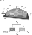
- FIG. 2 is a schematic diagram and a circuit diagram of an inverter device according to one embodiment of the present disclosure.
- an inverter device 20 may include the super-steep switching device 100 and a pull-up transistor 200.
- the super-steep switching device 100 includes the configuration as described above. Thus, the description thereof will be omitted.
- the pull-up transistor 200 may be connected in series with the super-steep switching device 100 and may operate in a complementary manner to the super-steep switching device 100.
- a gate electrode 210 of the pull-up transistor 200 and the gate electrode 150 of the super-steep switching device 100 are electrically connected to each other. Thus, the same gate voltage may be applied thereto.
- a semiconductor layer 220 of the pull-up transistor 200 may be made of an n-type semiconductor material capable of performing a complementary operation with the super-steep switching device.
- the semiconductor layer 220 of the pull-up transistor 200 may be made of an n-type semiconductor material such as molybdenum disulfide (MoS 2 ), indium selenide (In 2 Se 3 ), rhenium disulfide (ReS 2 ), or molybdenum diselenide (MoSe 2 ).
- the semiconductor layer 220 of the pull-up transistor 200 may be made of a p-type semiconductor material capable of performing a complementary operation with the super-steep switching device.
- the semiconductor layer 220 of the pull-up transistor 200 may be made of a p-type semiconductor material such as black phosphorus (BP), tungsten diselenide (WSe 2 ), boron arsenide (BAs), or tellurium.
- the inverter device 20 may exhibit a high inverter gain and ideal noise margin characteristic based on the super-steep switching phenomenon, due to a simple series connection circuit configuration between the super-steep switching device 100 and the pull-up transistor 200 that may operate in a complementary manner to the super-steep switching device 100.
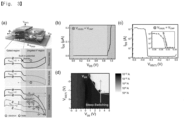
- FIG. 3 shows a schematic diagram of a WSe 2 homojunction transistor-based super-steep switching device according to one embodiment of the present disclosure, and a band structure diagram that changes based on a drain voltage and a top gate voltage.
- FIG. 3 shows output characteristic (ID-VD) and transfer characteristic (ID-VG), respectively, exhibiting a rapid increase in current based on the impact ionization phenomenon.
- (c) in FIG. 3 shows, as an inset, an enlarged graph of an area where super-steep switching takes place. Based on the graph, it may be identified that the device according to the present disclosure overcomes the thermionic limit of a CMOS device of 60 mV/dec and rather exhibits an SS value of 2.73 mV/dec.
- FIG. 3 is a contour diagram of a channel current changing based on the drain voltage and the top gate voltage and shows a steep-switching result measured via the impact ionization.
- a critical top gate voltage required for the steep-switching changes based on change in the applied drain voltage (higher than or equal to V BR determined based on a length of the ungated-region).
- V BR determined based on a length of the ungated-region
- FIG. 4 is a graph showing change in critical voltage V BR based on change in the length of the first area (Gated region) overlapping the gate electrode and in the length of the second area (Ungated I 2 region) non-overlapping the gate electrode.
- the off current increases as the length of the second area (L ungated ) decreases
- the On current increases as the length of the first area (L gated ) decreases.
- the length of the first area (L gated ) is fixed to 1 ⁇ m
- the length of the second area (L ungated ) changes.
- the SS value is a remarkably low value of 5 mV/dec or smaller.
- the On/Off ratio of the device and the SS value of the device may be optimized.
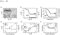
- FIG. 5 are respectively graphs showing transfer characteristic (ID-VG) and output characteristic (ID-VD) of WSe 2 having impact ionization characteristic.
- V DS ⁇ -15 V the impact ionization phenomenon due to a sharp increase in current under a high voltage (avalanche bias) of V DS ⁇ -15 V may be identified.
- (c) in FIG. 5 is a graph showing a result of analyzing the impact ionization characteristic of WSe 2 .
- M 1 / 1 ⁇ E E CR n
- E an electric field intensity
- E CR is a critical electric field intensity
- n an index related to an ionization scattering cross section
- WSe 2 exhibits a high multiplication factor value of up to 5000 and a low critical electric field intensity (Critical E-field) value of 25 KV/cm, and thus WSe 2 is an optimized material having the impact ionization.
- FIG. 5 shows changes in critical voltage V BR and critical electric field intensity E CR based on the length of the semiconductor channel according to the present disclosure. As shown in (d) in FIG. 5 , it may be identified that an operation voltage may be lowered as the semiconductor channel length is reduced.
- FIG. 5 shows the change in the critical electric field intensity E CR and the multiplication factor based on a thickness of the semiconductor channel according to the present disclosure.
- E critical electric field intensity
- (f) in FIG. 5 shows the change in the impact ionization characteristic based on a temperature. Only a small change of about 2.5 KV/cm may be observed based on the temperature change of 100 to 300 K. This corresponds to 2.5 ⁇ 10 -4 V/mm. Thus, the change in the operation voltage is 0.075 V at a channel length of about 300 nm. This supports the reason why the super-steep switching device according to the present disclosure operates even at room temperature.
- FIG. 6 is a schematic diagram and a circuit diagram of an inverter device according to one embodiment of the present disclosure in which a super-steep switching device and a pull-up transistor capable of performing a complementary operation therewith are connected in series with each other.
- V In denotes the top gate voltage
- V out denotes an output voltage between two transistors.
- FIG. 6 is a graph showing the transfer characteristic (ID-VG) of the inverter device according to one embodiment of the present disclosure. It may be identified that the inverter device has two stable logic state areas based on the complementary operation, based on a gate voltage of a green dot.
- (c) in FIG. 6 shows the V out -V in curve of the inverter device. Based on the curve, the inverter device operation in the series connection circuit structure of the two transistors may be identified. Further, referring to (c) in FIG. 6 , it may be identified that the inverter device has the high inverter gain value (Peak gain ⁇ 73) and the ideal noise margin (NML+NMH ⁇ 98.65% of VDD) resulting from the super-steep switching phenomenon.
- Peak gain ⁇ 73 the high inverter gain value
- NML+NMH ⁇ 98.65% of VDD ideal noise margin
Landscapes
- Engineering & Computer Science (AREA)
- Power Engineering (AREA)
- Insulated Gate Type Field-Effect Transistor (AREA)
- Junction Field-Effect Transistors (AREA)
- Metal-Oxide And Bipolar Metal-Oxide Semiconductor Integrated Circuits (AREA)
- Thin Film Transistor (AREA)
Abstract
Description
- The present disclosure relates to a super-steep switching device using avalanche carrier multiplication phenomenon and an inverter device using the same.
- In a conventional CMOS-based information processing device, excessive power loss/consumption due to high integration of the device has caused a power management problem, and performance thereof per watt has reached a limit thereof.
- Accordingly, efforts to overcome fundamental thermionic limit of the conventional CMOS-based information processing device are progressing at each of material, device, and architecture levels. For example, a steep-switching device such as a tunneling FET, a negative capacitance FET, and an I-MOS may be used.
- However, the above-described devices cause problems such as low reliability and instability due to problems such as high operation voltage required for operation of the devices, and damage of hot electrons caused by the high operation voltage to insulators and interfaces. In reality, a steep-switching device capable of operating at room temperature has not been realized.
- One purpose of the present disclosure is to provide a super-steep switching device having a very low SS (Subthreshold Swing) value even at room temperature using avalanche carrier multiplication phenomenon.
- Another purpose of the present disclosure is to provide an inverter device using the super-steep switching device.
- A first aspect of the present disclosure provides a super-steep switching device comprising: a semiconductor channel disposed on a substrate and made of a semiconductor material having impact ionization characteristic; a source electrode and a drain electrode in contact with the semiconductor channel, wherein the source electrode and the drain electrode are disposed on the substrate and are spaced apart from each other; and a gate electrode disposed on the semiconductor channel so as to overlap only a portion of the semiconductor channel, wherein a top surface of the semiconductor channel includes a first area overlapping the gate electrode, and a second area non-overlapping the gate electrode, wherein a ratio of a length of the first area and a length of the second area is in a range of 1: 0.1 to 0.4
- In one implementation of the super-steep switching device, a voltage for generating an electric field having an intensity higher than a critical electric field intensity, and lower than a breakdown electric field intensity is applied to the drain electrode, wherein the critical electric field intensity is a minimum electric field intensity at which avalanche carrier multiplication occurs in the first area, wherein the breakdown electric field intensity is an electric field intensity at which breakdown occurs in the first area.
- In one implementation of the super-steep switching device, a gate voltage is applied to the gate electrode simultaneously with the application of the voltage to the drain electrode, such that the avalanche carrier multiplication phenomenon occurs in the first area.
- In one implementation of the super-steep switching device, the super-steep switching device exhibits a subthreshold swing (SS) value smaller than or equal to 5 mV/dec at room temperature using the avalanche carrier multiplication phenomenon occurring in the first area.
- In one implementation of the super-steep switching device, the gate electrode overlaps the portion of the semiconductor channel closer to the source electrode than to the drain electrode.
- In one implementation of the super-steep switching device, the second area has the length in a range of 5 to 400 nm.
- In one implementation of the super-steep switching device, the semiconductor channel is made of one two-dimensional semiconductor material selected from a group consisting of black phosphorus (BP), tungsten diselenide (WSe2), indium selenide (InSe), molybdenum disulfide (MoS2), boron arsenide (BAs), indium selenide (In2Se3), zirconium diselenide (ZrSe2), and hafnium diselenide (HfSe2).
- A second aspect of the present disclosure provides an inverter device comprising: the super-steep switching device of the first aspect; and a pull-up transistor connected in series with the super-steep switching device, wherein the pull-up transistor is configured to perform a complementary operation with the super-steep switching device.
- In one implementation of the inverter device, a gate electrode of the pull-up transistor and the gate electrode of the super-steep switching device are electrically connected to each other so that the same gate voltage is applied thereto.
- In one implementation of the inverter device, a semiconductor layer of the pull-up transistor is made of a p-type or n-type semiconductor material capable of performing a complementary operation with the super-steep switching device, wherein the p-type semiconductor material includes one selected from a group consisting of black phosphorus (BP), tungsten diselenide (WSe2), boron arsenide (BAs) and tellurium, wherein the n-type semiconductor material includes one selected from a group consisting of molybdenum disulfide (MoS2), indium selenide (In2Se3), rhenium disulfide (ReS2) and molybdenum diselenide (MoSe2).
- In the super-steep switching device according to the present disclosure, the gate area is controlled using a structure in which the gate electrode overlaps only the portion of the semiconductor channel having the impact ionization characteristic. The gate voltage gradually increases while the electric field having the intensity greater than the critical electric field intensity is applied to the semiconductor channel. Thus, the probability of occurrence of avalanche carrier multiplication may increase. As a result, the number of charge carriers generated in the semiconductor channel may be significantly increased. As a result, the super-steep switching device having a very low SS (Subthreshold Swing) value may be implemented even at room temperature.
- Further, according to the present disclosure, the inverter device having a high inverter gain and ideal noise margin based on the super-steep switching phenomenon using a simple series connection circuit configuration between the super-steep switching device and the pull-up transistor capable of performing the complementary operation with the super-steep switching device may be implemented.
-
-
FIG. 1 is a cross-sectional view for illustrating a super-steep switching device according to one embodiment of the present disclosure. -
FIG. 2 is a schematic diagram and a circuit diagram of an inverter device according to one embodiment of the present disclosure. In this regard, VIn denotes a top gate voltage and Vout denotes an output voltage between two transistors. - (a) in
FIG. 3 shows a schematic diagram of a WSe2 homojunction transistor-based super-steep switching device according to one embodiment of the present disclosure, and a band structure diagram that changes based on a drain voltage and a top gate voltage. (b) and (c) inFIG. 3 are graphs respectively showing output characteristic (ID-VD) and transfer characteristic (ID-VG) exhibiting a sudden increase in current based on the impact ionization phenomenon. (d) inFIG. 3 is a contour diagram of a channel current that changes based on a drain voltage and a top gate voltage. - (a) in
FIG. 4 is a graph showing change in critical voltage VBR based on change in the length of the first area (Gated region) overlapping the gate electrode and in the length of the second area (Ungated I2 region) non-overlapping the gate electrode. (b) inFIG. 4 is a graph showing a probability of occurrence of impact ionization based on a change in a ratio of the length of the second area to the length of the first area. (c) inFIG. 4 is a graph showing the change in the on/off current based on the change in a ratio of the length of the second area to the length of the first area. (d) inFIG. 4 is a graph showing the change in the on/off ratio and SS (Subthreshold Swing) value based on the change in a ratio of the length of the second area to the length of the first area. - (a) and (b) in
FIG. 5 are respectively graphs showing transfer characteristic (ID-VG) and output characteristic (ID-VD) of WSe2 having impact ionization characteristic. (c) inFIG. 5 is a graph of the multiplication factor based on the electric field (E-field) calculated from the output characteristic (ID-VD). (d) inFIG. 5 is a graph showing the change in the critical voltage VBR and the critical electric field intensity ECR based on the length of the semiconductor channel according to the present disclosure, (e) inFIG. 5 is a graph showing the change in the critical electric field intensity ECR and the change in the multiplication factor under the same electric field (E = 52 kV/cm) based on a thickness of the semiconductor channel according to the present disclosure. (f) inFIG. 5 is a graph showing the change in drain current-electric field based on a temperature. - (a) in
FIG. 6 is a schematic diagram and a circuit diagram of an inverter device according to one embodiment of the present disclosure in which a super-steep switching device and a pull-up transistor capable of performing a complementary operation therewith are connected in series with each other. In this regard, VIn denotes the top gate voltage and Vout denotes an output voltage between two transistors. - (b) in
FIG. 6 is a graph showing the transfer characteristic (ID-VG) of the inverter device according to one embodiment of the present disclosure. (c) inFIG. 6 shows the Vout-Vin curve of the inverter device. - Hereinafter, an embodiment of the present disclosure will be described in detail with reference to the accompanying drawings. In the present disclosure, various changes may be made. The present disclosure may have various forms. Thus, specific embodiments may be illustrated in the drawings and may be described in detail herein. However, the embodiments are not intended to limit the present disclosure to a specific form. It should be understood that the present disclosure may include all changes, equivalents or substitutes included in the spirit and scope of the present disclosure. In illustrating the drawings, like reference numerals have been used for like elements.
- The terminology used herein is for the purpose of describing particular embodiments only and is not intended to be limiting of the present disclosure. As used herein, the singular forms "a" and "an" are intended to include the plural forms as well, unless the context clearly indicates otherwise. It will be further understood that the terms "comprises", "comprising", "includes", and "including" when used in this specification, specify the presence of the stated features, integers, operations, elements, and/or components, but do not preclude the presence or addition of one or greater other features, integers, operations, elements, components, and/or portions thereof.
- Unless otherwise defined, all terms including technical and scientific terms used herein have the same meaning as commonly understood by one of ordinary skill in the art to which this inventive concept belongs. It will be further understood that terms, such as those defined in commonly used dictionaries, should be interpreted as having a meaning that is consistent with their meaning in the context of the relevant art and will not be interpreted in an idealized or overly formal sense unless expressly so defined herein.
-
FIG. 1 is a cross-sectional view for illustrating a super-steep switching device according to one embodiment of the present disclosure. - Referring to
FIG. 1 , asuper-steep switching device 100 according to one embodiment of the present disclosure may include asubstrate 110, asemiconductor channel 120, asource electrode 130, adrain electrode 140, and agate electrode 150. - A type of the
substrate 110 is not particularly limited as long as the substate may support thesemiconductor channel 120, thesource electrode 130, and thedrain electrode 140 thereon. For example, thesubstrate 110 may include one selected from a metal having an insulating film formed on a surface thereof, a semiconductor substrate, a ceramic substrate, a polymer substrate, and the like. - The
semiconductor channel 120 may be disposed on thesubstrate 110. Thesemiconductor channel 120 may be made of a semiconductor material having impact ionization characteristic. Thesemiconductor channel 120 may be made of a p-type semiconductor material or an n-type semiconductor material. For example, thesemiconductor channel 120 is made of a two-dimensional p-type semiconductor material such as black phosphorus (BP), tungsten diselenide (WSe2), boron arsenide (BAs), or etc. or may be made of a two-dimensional n-type semiconductor material such as indium selenide (InSe), molybdenum disulfide (MoS2), indium selenide (In2Se3), zirconium diselenide (ZrSe2), hafnium diselenide (HfSe2), etc. - In one embodiment, the
semiconductor channel 120 may be made of a material having a relatively low bandgap. This is because, as the band gap of thesemiconductor channel 120 is smaller, an intensity of a critical electric field intensity that causes avalanche carrier multiplication, which will be described below, may be reduced. For example, thesemiconductor channel 120 may be made of a semiconductor material having a bandgap of about 0.3 to 1.9 eV. - The
source electrode 130 and thedrain electrode 140 may be in contact with thesemiconductor channel 120 while being disposed on thesubstrate 110 and being spaced apart from each other. An area of thesemiconductor channels 120 between thesource electrode 130 and thedrain electrode 140 may constitute a channel through which current may flow. Each of the source and drainelectrodes - The
gate electrode 150 may be disposed on thesemiconductor channel 120 so as to overlap only a portion of thesemiconductor channel 120, and may receive a voltage so as to generate an electric field in thesemiconductor channel 120. In one embodiment, thegate electrode 150 may be disposed so as to overlap only a portion of thesemiconductor channel 120 adjacent to thesource electrode 130. Further, an insulatinglayer 151 may be formed between thegate electrode 150 and thesemiconductor channel 120. - In one embodiment, a top surface of the
semiconductor channel 120 may include a first area A overlapping thegate electrode 150, and a second area B non-overlapping thegate electrode 150. A ratio of a length of the first area A and a length of the second area B may be adjusted to control characteristic of the super-steep switching device. - In one embodiment, in a device structure in which the first area A and the second area B are formed, a voltage for generating an electric field having an intensity greater than a minimum electric field intensity (hereinafter, referred to as a 'critical electric field intensity') at which the avalanche multiplication occurs in the first area A may be applied to the
drain electrode 140. - Further, a voltage may be applied to the
gate electrode 150 simultaneously with the voltage application to thedrain electrode 140. As the gate voltage gradually increases, the avalanche carrier multiplication phenomenon may occur in the first area A. That is, while the electric field having the intensity above the critical electric field intensity is applied to the first area A under the voltage application to thedrain electrode 140, the gate voltage is gradually increased to generate the avalanche carrier multiplication, thereby implementing super-steep switching phenomenon at room temperature. - When the electric field is applied to the first area A, the charge carriers are accelerated in the first area A. In general, the velocity of the charge carriers does not increase indefinitely. Rather, due to impact thereof with the lattice, the velocity of the charge carriers is saturated at a constant level. However, when a sufficiently strong electric field, that is, an electric field having the intensity larger than the critical electric field intensity is applied, the charge carriers sufficiently accelerated under the electric field collide with the lattice to cause an electron in the valence band to transfer to the conduction band, such that a new electron-hole pair is created. The new electron-hole pair again acquires high energy to continuously generate additional electron-hole pairs, and thus the carrier density may be greatly increased. In the present disclosure, the avalanche multiplication means that carriers are multiplicated under the impact ionization as described above, and the critical electric field intensity indicates the minimum electric field intensity at which the avalanche multiplication occurs.
- In one embodiment, regarding dark current change characteristic based on the electric field to the first area A, when the electric field having an intensity below the critical electric field intensity is applied to the first area A, a magnitude of the dark current generated in the first area A increases linearly based son the intensity of the applied electric field. To the contrary, when an electric field having an intensity larger than the critical electric field intensity is applied thereto, the magnitude of the dark current generated in the first area A increases in a superlinear manner due to the avalanche multiplication. Accordingly, the critical electric field intensity may refer to an electric field intensity at a point where behavior of the dark current changes from a linear manner to the superlinear manner in the dark current change characteristic based son the electric field for the first area A.
- In this regard, when the intensity of the electric field applied to the first area A greater than the critical electric field intensity continuously increases, breakdown of the first area A occurs. Accordingly, the
drain electrode 140 may apply, to thesemiconductor channel 120, an electric field having an intensity that is greater than the critical electric field intensity and is lower than the intensity of the electric field at which breakdown of thesemiconductor channel 120 occurs. - In one example, as described above, according to the present disclosure, the ratio of the length of the first area A and the length of the second area B may be controlled to implement the super-steep switching device that exhibits a low SS (Subthreshold Swing) value even at room temperature. In this regard, the SS (Subthreshold Swing) means a VGS value required to increase a drain-source current IDS by 10 times in a field effect transistor.
- In one embodiment, the second area B may have a length greater than 5 nm so that a tunneling phenomenon does not occur therein, and may have the length smaller than 400 nm so that steep switching may be possible. The second area B may have a length smaller than 400 nm so that a steep-switching phenomenon does not occur therein. For an optimized operation of the super-steep switching device according to this embodiment, the ratio of the length of the first area A and the length of the second area B may be in a range of 1:0.1 to 0.4.
- When the ratio of the length of the second area to the length of the first area A is smaller than 0.1, an off current increases such that an on/off ratio decreases as, and thus the SS value increases, and thus, probability of occurrence of impact ionization decreases. On the contrary, when the ratio of the length of the second area B to the length of the first area A exceeds 0.4, the steep-switching does not occur.
- However, in the super-steep switching device of this embodiment, a length of a gate area of the
semiconductor channel 120 having impact ionization characteristic may be adjusted as described above, thereby increasing the probability of occurrence of the avalanche carrier multiplication phenomenon occurring in the first area A, and thus, significantly increasing the number of charge carriers generated in thesemiconductor channel 120. As a result, the super-steep switching device having a very low (5mv/dec or lower) SS (Subthreshold Swing) value even at room temperature and having an optimized On/Off ratio may be implemented. -
FIG. 2 is a schematic diagram and a circuit diagram of an inverter device according to one embodiment of the present disclosure. - Referring to
FIG. 2 , aninverter device 20 according to one embodiment of the present disclosure may include thesuper-steep switching device 100 and a pull-uptransistor 200. - The
super-steep switching device 100 includes the configuration as described above. Thus, the description thereof will be omitted. - The pull-up
transistor 200 may be connected in series with thesuper-steep switching device 100 and may operate in a complementary manner to thesuper-steep switching device 100. - In one embodiment, a
gate electrode 210 of the pull-uptransistor 200 and thegate electrode 150 of thesuper-steep switching device 100 are electrically connected to each other. Thus, the same gate voltage may be applied thereto. - In one embodiment, a
semiconductor layer 220 of the pull-uptransistor 200 may be made of an n-type semiconductor material capable of performing a complementary operation with the super-steep switching device. For example, thesemiconductor layer 220 of the pull-uptransistor 200 may be made of an n-type semiconductor material such as molybdenum disulfide (MoS2), indium selenide (In2Se3), rhenium disulfide (ReS2), or molybdenum diselenide (MoSe2). - In one embodiment, the
semiconductor layer 220 of the pull-uptransistor 200 may be made of a p-type semiconductor material capable of performing a complementary operation with the super-steep switching device. For example, thesemiconductor layer 220 of the pull-uptransistor 200 may be made of a p-type semiconductor material such as black phosphorus (BP), tungsten diselenide (WSe2), boron arsenide (BAs), or tellurium. - The
inverter device 20 according to the present disclosure may exhibit a high inverter gain and ideal noise margin characteristic based on the super-steep switching phenomenon, due to a simple series connection circuit configuration between thesuper-steep switching device 100 and the pull-uptransistor 200 that may operate in a complementary manner to thesuper-steep switching device 100. - Hereinafter, Examples of the present disclosure will be described in detail. However, the following Examples are only some examples of the present disclosure, and the scope of the present disclosure is not limited to the following Examples.
- (a) in
FIG. 3 shows a schematic diagram of a WSe2 homojunction transistor-based super-steep switching device according to one embodiment of the present disclosure, and a band structure diagram that changes based on a drain voltage and a top gate voltage. - Referring to (a) in
FIG. 3 , it may be identified that when sufficiently high drain voltage (Avalanche bias) and top gate voltage are applied, the impact ionization occurs in the second area (Ungated I2 region) non-overlapping the gate electrode. - Further, (b) and (c) in
FIG. 3 show output characteristic (ID-VD) and transfer characteristic (ID-VG), respectively, exhibiting a rapid increase in current based on the impact ionization phenomenon. (c) inFIG. 3 shows, as an inset, an enlarged graph of an area where super-steep switching takes place. Based on the graph, it may be identified that the device according to the present disclosure overcomes the thermionic limit of a CMOS device of 60 mV/dec and rather exhibits an SS value of 2.73 mV/dec. - (d) in
FIG. 3 is a contour diagram of a channel current changing based on the drain voltage and the top gate voltage and shows a steep-switching result measured via the impact ionization. Referring toFIG. 3(d) , it may be identified that a critical top gate voltage required for the steep-switching changes based on change in the applied drain voltage (higher than or equal to VBR determined based on a length of the ungated-region). On the contrary, it may be identified when the drain voltage smaller than VBR is applied, the channel current stays at a saturated current. - (a) in
FIG. 4 is a graph showing change in critical voltage VBR based on change in the length of the first area (Gated region) overlapping the gate electrode and in the length of the second area (Ungated I2 region) non-overlapping the gate electrode. - As shown (a) in in
FIG. 4 , it may be identified that as both the length of the first area (Gated region) overlapping the gate electrode and the length of the second area (Ungated I2 region) which does not overlap the gate electrode are smaller, the critical voltage VBR decreases. - However, since device characteristic must be based on the critical voltage as well as the On/Off ratio, and the SS value, the probability of occurrence of impact ionization, the On/Off current ratio, and the SS value, based on the ratio of the length of the first area (Gated region) and the length of the second area (Ungated I2 region) which does not overlap the gate electrode were measured and were shown in (b) to (d) in
FIG. 4 respectively. - First, referring to (b) to (d) in
FIG. 4 , it may be identified that the off current increases as the length of the second area (Lungated) decreases, and the On current increases as the length of the first area (Lgated) decreases. Considering these results, the length of the first area (Lgated) is fixed to 1 µm, and the length of the second area (Lungated) changes. Thus, it may be identified that when the length of the second area (Lungated) is in a range of 100 to 400 nm, there is little change in the On current and Off current, the SS value is a remarkably low value of 5 mV/dec or smaller. - However, it is identified that when the ratio of the length of the second area (Lungated) to the length of the first area (Lgated) is smaller than 0.1 (that is, the length of the second area (Lungated) is smaller than 100 nm), the Off current suddenly increases such that the On/Off ratio decreases. Thus, the SS value increases.
- Further, as shown in (b) in
FIG. 4 , it may be identified that when the length of the second area is in a range of 100 to 400 nm based on the length of 1 µm of the first area, the probability of occurrence of impact ionization is high. However, it may be identified that when the length of the second area (Lungated) is smaller than 100 nm, the probability of occurrence of impact ionization is reduced. It may be identified that when the length of the second area (Lungated) exceeds 400 nm, the steep-switching does not occur. - From these results, it may be identified that when the ratio of the length of the first area and the length of the second area is in a range of 1:0. 1 to 0.4 in accordance with the present disclosure, the On/Off ratio of the device and the SS value of the device may be optimized.
- (a) and (b) in
FIG. 5 are respectively graphs showing transfer characteristic (ID-VG) and output characteristic (ID-VD) of WSe2 having impact ionization characteristic. - Referring to (a) and (b) of
FIG. 5 , the impact ionization phenomenon due to a sharp increase in current under a high voltage (avalanche bias) of VDS < -15 V may be identified. - (c) in
FIG. 5 is a graph showing a result of analyzing the impact ionization characteristic of WSe2. - The impact ionization characteristic was analyzed based on a following equation:

- Referring to (c) of
FIG. 5 , it may be identified that WSe2 exhibits a high multiplication factor value of up to 5000 and a low critical electric field intensity (Critical E-field) value of 25 KV/cm, and thus WSe2 is an optimized material having the impact ionization. - (d) in
FIG. 5 shows changes in critical voltage VBR and critical electric field intensity ECR based on the length of the semiconductor channel according to the present disclosure. As shown in (d) inFIG. 5 , it may be identified that an operation voltage may be lowered as the semiconductor channel length is reduced. - (e) in
FIG. 5 shows the change in the critical electric field intensity ECR and the multiplication factor based on a thickness of the semiconductor channel according to the present disclosure. As shown in (e) inFIG. 5 , it may be identified that as the thickness of the semiconductor channel decreases, the energy bandgap of the channel increases, and accordingly, the critical electric field intensity ECR also increases. Further, for comparison, regarding the multiplication factor under the same electric field condition (E=52 kV/cm), it may be identified that the multiplication factor decreases as the thickness of the semiconductor channel decreases. - (f) in
FIG. 5 shows the change in the impact ionization characteristic based on a temperature. Only a small change of about 2.5 KV/cm may be observed based on the temperature change of 100 to 300 K. This corresponds to 2.5 × 10⁻⁴ V/mm. Thus, the change in the operation voltage is 0.075 V at a channel length of about 300 nm. This supports the reason why the super-steep switching device according to the present disclosure operates even at room temperature. - (a) in
FIG. 6 is a schematic diagram and a circuit diagram of an inverter device according to one embodiment of the present disclosure in which a super-steep switching device and a pull-up transistor capable of performing a complementary operation therewith are connected in series with each other. In this regard, VIn denotes the top gate voltage and Vout denotes an output voltage between two transistors. - (b) in
FIG. 6 is a graph showing the transfer characteristic (ID-VG) of the inverter device according to one embodiment of the present disclosure. It may be identified that the inverter device has two stable logic state areas based on the complementary operation, based on a gate voltage of a green dot. - (c) in
FIG. 6 shows the Vout-Vin curve of the inverter device. Based on the curve, the inverter device operation in the series connection circuit structure of the two transistors may be identified. Further, referring to (c) inFIG. 6 , it may be identified that the inverter device has the high inverter gain value (Peak gain ~ 73) and the ideal noise margin (NML+NMH ~ 98.65% of VDD) resulting from the super-steep switching phenomenon. - Although the above description has been made with reference to a preferred embodiment of the present disclosure, those skilled in the art may variously modify and change the present disclosure without departing from the spirit and scope of the present disclosure as described in the claims below.
Claims (10)
- A super-steep switching device comprising:a semiconductor channel disposed on a substrate and made of a semiconductor material having impact ionization characteristic;a source electrode and a drain electrode in contact with the semiconductor channel, wherein the source electrode and the drain electrode are disposed on the substrate and are spaced apart from each other; anda gate electrode disposed on the semiconductor channel so as to overlap only a portion of the semiconductor channel,wherein a top surface of the semiconductor channel includes a first area overlapping the gate electrode, and a second area non-overlapping the gate electrode, wherein a ratio of a length of the first area and a length of the second area is in a range of 1: 0.1 to 0.4
- The super-steep switching device of claim 1, wherein a voltage for generating an electric field having an intensity higher than a critical electric field intensity, and lower than a breakdown electric field intensity is applied to the drain electrode,wherein the critical electric field intensity is a minimum electric field intensity at which avalanche carrier multiplication occurs in the first area,wherein the breakdown electric field intensity is an electric field intensity at which breakdown occurs in the first area.
- The super-steep switching device of claim 2, wherein a gate voltage is applied to the gate electrode simultaneously with the application of the voltage to the drain electrode, such that the avalanche carrier multiplication phenomenon occurs in the first area.
- The super-steep switching device of claim 3, wherein the super-steep switching device exhibits a subthreshold swing (SS) value smaller than or equal to 5 mV/dec at room temperature using the avalanche carrier multiplication phenomenon occurring in the first area.
- The super-steep switching device of claim 1, wherein the gate electrode overlaps the portion of the semiconductor channel closer to the source electrode than to the drain electrode.
- The super-steep switching device of claim 1, wherein the second area has the length in a range of 5 to 400 nm.
- The super-steep switching device of claim 1, wherein the semiconductor channel is made of one two-dimensional semiconductor material selected from a group consisting of black phosphorus (BP), tungsten diselenide (WSe2), indium selenide (InSe), molybdenum disulfide (MoS2), boron arsenide (BAs), indium selenide (In2Se3), zirconium diselenide (ZrSe2), and hafnium diselenide (HfSe2).
- An inverter device comprising:the super-steep switching device according to one of claims 1 to 7; anda pull-up transistor connected in series with the super-steep switching device,wherein the pull-up transistor is configured to perform an complementary operation with the super-steep switching device.
- The inverter device of claim 8, wherein a gate electrode of the pull-up transistor and the gate electrode of the super-steep switching device are electrically connected to each other so that the same gate voltage is applied thereto.
- The inverter device of claim 8, wherein a semiconductor layer of the pull-up transistor is made of a p-type or n-type semiconductor material capable of performing a complementary operation with the super-steep switching device,wherein the p-type semiconductor material includes one selected from a group consisting of black phosphorus (BP), tungsten diselenide (WSe2), boron arsenide (BAs) and tellurium,wherein the n-type semiconductor material includes one selected from a group consisting of molybdenum disulfide (MoS2), indium selenide (In2Se3), rhenium disulfide (ReS2) and molybdenum diselenide (MoSe2).
Applications Claiming Priority (2)
| Application Number | Priority Date | Filing Date | Title |
|---|---|---|---|
| KR1020210119491A KR102655078B1 (en) | 2021-09-08 | 2021-09-08 | Superlinear switching device and inverter device element using same |
| PCT/KR2022/013545 WO2023038465A1 (en) | 2021-09-08 | 2022-09-08 | Super tilt switching element and inverter element using same |
Publications (3)
| Publication Number | Publication Date |
|---|---|
| EP4401146A1 true EP4401146A1 (en) | 2024-07-17 |
| EP4401146A4 EP4401146A4 (en) | 2025-04-23 |
| EP4401146B1 EP4401146B1 (en) | 2026-03-11 |
Family
ID=85506835
Family Applications (1)
| Application Number | Title | Priority Date | Filing Date |
|---|---|---|---|
| EP22867733.2A Active EP4401146B1 (en) | 2021-09-08 | 2022-09-08 | Super-steep switching element and inverter element using same |
Country Status (5)
| Country | Link |
|---|---|
| US (2) | US12484300B2 (en) |
| EP (1) | EP4401146B1 (en) |
| JP (1) | JP7580170B2 (en) |
| KR (2) | KR102655078B1 (en) |
| WO (1) | WO2023038465A1 (en) |
Families Citing this family (1)
| Publication number | Priority date | Publication date | Assignee | Title |
|---|---|---|---|---|
| KR102863834B1 (en) * | 2024-06-13 | 2025-09-25 | 기초과학연구원 | Semiconductor device and manufacturing method thereof |
Family Cites Families (15)
| Publication number | Priority date | Publication date | Assignee | Title |
|---|---|---|---|---|
| US3821657A (en) * | 1972-10-25 | 1974-06-28 | Gen Electric | High frequency semiconductor amplifying devices and circuits therefor |
| KR100804738B1 (en) | 2007-01-16 | 2008-02-19 | 삼성전자주식회사 | Semiconductor Probe Using Ionization Impingement Semiconductor Device, Information Storage Device Having Same and Manufacturing Method Thereof |
| KR100995535B1 (en) | 2009-02-11 | 2010-11-22 | 한국과학기술원 | Flash Memory Using Collision Ionization Metal Oxide Semiconductors |
| JP2011165921A (en) | 2010-02-10 | 2011-08-25 | Renesas Electronics Corp | Semiconductor device, logic circuit and manufacturing method thereof |
| JP6589552B2 (en) * | 2015-10-22 | 2019-10-16 | 富士通株式会社 | Electronic device and method for manufacturing electronic device |
| US11393923B2 (en) * | 2016-02-25 | 2022-07-19 | Indian Institute Of Science | Drain extended tunnel field effect transistor |
| US10043808B1 (en) | 2017-03-16 | 2018-08-07 | Toshiba Memory Corporation | Semiconductor memory |
| US10411695B2 (en) * | 2017-05-26 | 2019-09-10 | Indian Institute Of Science | Programmable tunnel thermionic mode transistor |
| KR101949504B1 (en) * | 2017-06-12 | 2019-02-18 | 성균관대학교산학협력단 | Semiconductor device with negative differential transconductance and its manufacturing method |
| KR101966531B1 (en) * | 2017-07-05 | 2019-04-05 | 성균관대학교산학협력단 | Tunneling field effect transistor |
| US10879368B2 (en) | 2017-10-17 | 2020-12-29 | Mitsubishi Electric Research Laboratories, Inc. | Transistor with multi-metal gate |
| US11082039B2 (en) * | 2017-11-08 | 2021-08-03 | Gan Systems Inc. | GaN transistor with integrated drain voltage sense for fast overcurrent and short circuit protection |
| JP7475327B2 (en) | 2019-03-12 | 2024-04-26 | 株式会社半導体エネルギー研究所 | SEMICONDUCTOR DEVICE AND METHOD FOR MANUFACTURING SEMICONDUCTOR DEVICE |
| JP7362352B2 (en) * | 2019-08-23 | 2023-10-17 | キヤノン株式会社 | Photoelectric conversion devices, photoelectric conversion systems, and mobile objects |
| KR102271098B1 (en) * | 2019-11-07 | 2021-06-29 | 성균관대학교산학협력단 | Photo detecting device, method of manufacturing the photo detecting device, and method of detecting light using the photo detecting device |
-
2021
- 2021-09-08 KR KR1020210119491A patent/KR102655078B1/en active Active
-
2022
- 2022-09-08 US US18/014,078 patent/US12484300B2/en active Active
- 2022-09-08 EP EP22867733.2A patent/EP4401146B1/en active Active
- 2022-09-08 JP JP2024514727A patent/JP7580170B2/en active Active
- 2022-09-08 WO PCT/KR2022/013545 patent/WO2023038465A1/en not_active Ceased
-
2024
- 2024-03-07 US US18/598,689 patent/US12211849B2/en active Active
- 2024-03-14 KR KR1020240035526A patent/KR102777691B1/en active Active
Also Published As
| Publication number | Publication date |
|---|---|
| EP4401146A4 (en) | 2025-04-23 |
| WO2023038465A1 (en) | 2023-03-16 |
| US12211849B2 (en) | 2025-01-28 |
| KR102777691B1 (en) | 2025-03-06 |
| US20240213376A1 (en) | 2024-06-27 |
| JP2024532925A (en) | 2024-09-10 |
| EP4401146B1 (en) | 2026-03-11 |
| KR20230036679A (en) | 2023-03-15 |
| US12484300B2 (en) | 2025-11-25 |
| US20240096888A1 (en) | 2024-03-21 |
| JP7580170B2 (en) | 2024-11-11 |
| KR102655078B1 (en) | 2024-04-05 |
| KR20240044393A (en) | 2024-04-04 |
Similar Documents
| Publication | Publication Date | Title |
|---|---|---|
| Padilla et al. | Feedback FET: A novel transistor exhibiting steep switching behavior at low bias voltages | |
| US4882295A (en) | Method of making a double injection field effect transistor | |
| US9583566B2 (en) | Reduced scale resonant tunneling field effect transistor | |
| KR101966531B1 (en) | Tunneling field effect transistor | |
| Kastalsky et al. | Novel real-space hot-electron transfer devices | |
| Bencherif et al. | Temperature and SiO2/4H-SiC interface trap effects on the electrical characteristics of low breakdown voltage MOSFETs | |
| US12211849B2 (en) | Super-steep switching device and inverter device using the same | |
| KR20010032538A (en) | Field effect transistor | |
| KR101576267B1 (en) | Esaki Tunneling Assisted Tunnel Field-Effect Transistor | |
| EP0278386B1 (en) | Heterojunction bipolar transistor | |
| US4183033A (en) | Field effect transistors | |
| Burdeaux et al. | Intrinsic reliability of RF power LDMOS FETs | |
| Shaikh et al. | Electrostatically doped drain engineered DG‐TFET: Proposal and analysis | |
| CN210224032U (en) | SOI transverse constant current diode | |
| Adinarayana et al. | Design and development of a high-efficient nanowire fet for emerging logic devices | |
| DeSalvo | Silicon carbide static induction transistors | |
| Srivastava et al. | Optimizing Gallium Nitride (GaN) Based SOI-TF-FinFETs for Enhanced Linearity and Low Distortion in High-Frequency Applications | |
| KR102944532B1 (en) | Multifunctional ambipolar filed effect transistor with partially gated channel | |
| CA1189981A (en) | Punch through modulated semiconductor device | |
| Colinge et al. | A lateral COMFET made in thin silicon-on-insulator film | |
| Jiang et al. | High Current Density and High Breakdown Voltage Enhancement-Mode Gate-Controlled Heterojunction Vertical β-Ga 2 O 3 MOSFET | |
| Som et al. | Dopingless SOI Schottky Barrier | |
| Kumar et al. | Investigating the Device and Circuit Level Performance of Nanoscale Double Gate Junctionless Transistors | |
| Mohanta et al. | Si Vertical TFET with Triple Metal Gate for Low Power Application | |
| Kumar et al. | Simulation Study of Charge Plasma Nanotube FET for Low Power Mixed Signal Circuit in IoT Applications |
Legal Events
| Date | Code | Title | Description |
|---|---|---|---|
| STAA | Information on the status of an ep patent application or granted ep patent |
Free format text: STATUS: THE INTERNATIONAL PUBLICATION HAS BEEN MADE |
|
| PUAI | Public reference made under article 153(3) epc to a published international application that has entered the european phase |
Free format text: ORIGINAL CODE: 0009012 |
|
| STAA | Information on the status of an ep patent application or granted ep patent |
Free format text: STATUS: REQUEST FOR EXAMINATION WAS MADE |
|
| 17P | Request for examination filed |
Effective date: 20240313 |
|
| AK | Designated contracting states |
Kind code of ref document: A1 Designated state(s): AL AT BE BG CH CY CZ DE DK EE ES FI FR GB GR HR HU IE IS IT LI LT LU LV MC MK MT NL NO PL PT RO RS SE SI SK SM TR |
|
| DAV | Request for validation of the european patent (deleted) | ||
| DAX | Request for extension of the european patent (deleted) | ||
| REG | Reference to a national code |
Ref country code: DE Ref legal event code: R079 Free format text: PREVIOUS MAIN CLASS: H01L0029739000 Ipc: H10D0030470000 Ref country code: DE Ref legal event code: R079 Ref document number: 602022032311 Country of ref document: DE Free format text: PREVIOUS MAIN CLASS: H01L0029739000 Ipc: H10D0030470000 |
|
| A4 | Supplementary search report drawn up and despatched |
Effective date: 20250320 |
|
| RIC1 | Information provided on ipc code assigned before grant |
Ipc: H10D 62/10 20250101ALI20250314BHEP Ipc: H10D 64/27 20250101ALI20250314BHEP Ipc: H10D 30/67 20250101ALI20250314BHEP Ipc: H10D 84/85 20250101ALI20250314BHEP Ipc: H10D 84/02 20250101ALI20250314BHEP Ipc: H10D 62/80 20250101ALI20250314BHEP Ipc: H10D 30/47 20250101AFI20250314BHEP |
|
| RIC1 | Information provided on ipc code assigned before grant |
Ipc: H10D 30/47 20250101AFI20251126BHEP Ipc: H10D 62/80 20250101ALI20251126BHEP Ipc: H10D 84/02 20250101ALI20251126BHEP Ipc: H10D 84/85 20250101ALI20251126BHEP Ipc: H10D 30/67 20250101ALI20251126BHEP Ipc: H10D 64/27 20250101ALI20251126BHEP Ipc: H10D 62/10 20250101ALI20251126BHEP |
|
| GRAP | Despatch of communication of intention to grant a patent |
Free format text: ORIGINAL CODE: EPIDOSNIGR1 |
|
| STAA | Information on the status of an ep patent application or granted ep patent |
Free format text: STATUS: GRANT OF PATENT IS INTENDED |
|
| INTG | Intention to grant announced |
Effective date: 20260105 |
|
| GRAS | Grant fee paid |
Free format text: ORIGINAL CODE: EPIDOSNIGR3 |
|
| GRAA | (expected) grant |
Free format text: ORIGINAL CODE: 0009210 |
|
| STAA | Information on the status of an ep patent application or granted ep patent |
Free format text: STATUS: THE PATENT HAS BEEN GRANTED |
|
| AK | Designated contracting states |
Kind code of ref document: B1 Designated state(s): AL AT BE BG CH CY CZ DE DK EE ES FI FR GB GR HR HU IE IS IT LI LT LU LV MC MK MT NL NO PL PT RO RS SE SI SK SM TR |
|
| REG | Reference to a national code |
Ref country code: CH Ref legal event code: F10 Free format text: ST27 STATUS EVENT CODE: U-0-0-F10-F00 (AS PROVIDED BY THE NATIONAL OFFICE) Effective date: 20260311 Ref country code: GB Ref legal event code: FG4D |
|
| REG | Reference to a national code |
Ref country code: DE Ref legal event code: R096 Ref document number: 602022032311 Country of ref document: DE |
|
| REG | Reference to a national code |
Ref country code: IE Ref legal event code: FG4D |