EP4401125A2 - Eliminating substrate metal cracks in a ball grid array package - Google Patents
Eliminating substrate metal cracks in a ball grid array package Download PDFInfo
- Publication number
- EP4401125A2 EP4401125A2 EP23216202.4A EP23216202A EP4401125A2 EP 4401125 A2 EP4401125 A2 EP 4401125A2 EP 23216202 A EP23216202 A EP 23216202A EP 4401125 A2 EP4401125 A2 EP 4401125A2
- Authority
- EP
- European Patent Office
- Prior art keywords
- die
- recessed portion
- solder mask
- planar surface
- attach material
- Prior art date
- Legal status (The legal status is an assumption and is not a legal conclusion. Google has not performed a legal analysis and makes no representation as to the accuracy of the status listed.)
- Pending
Links
Images



Classifications
-
- G—PHYSICS
- G11—INFORMATION STORAGE
- G11C—STATIC STORES
- G11C5/00—Details of stores covered by group G11C11/00
- G11C5/02—Disposition of storage elements, e.g. in the form of a matrix array
- G11C5/04—Supports for storage elements, e.g. memory modules; Mounting or fixing of storage elements on such supports
-
- H—ELECTRICITY
- H10—SEMICONDUCTOR DEVICES; ELECTRIC SOLID-STATE DEVICES NOT OTHERWISE PROVIDED FOR
- H10W—GENERIC PACKAGES, INTERCONNECTIONS, CONNECTORS OR OTHER CONSTRUCTIONAL DETAILS OF DEVICES COVERED BY CLASS H10
- H10W42/00—Arrangements for protection of devices
- H10W42/121—Arrangements for protection of devices protecting against mechanical damage
-
- H—ELECTRICITY
- H10—SEMICONDUCTOR DEVICES; ELECTRIC SOLID-STATE DEVICES NOT OTHERWISE PROVIDED FOR
- H10W—GENERIC PACKAGES, INTERCONNECTIONS, CONNECTORS OR OTHER CONSTRUCTIONAL DETAILS OF DEVICES COVERED BY CLASS H10
- H10W70/00—Package substrates; Interposers; Redistribution layers [RDL]
- H10W70/01—Manufacture or treatment
- H10W70/05—Manufacture or treatment of insulating or insulated package substrates, or of interposers, or of redistribution layers
-
- H—ELECTRICITY
- H10—SEMICONDUCTOR DEVICES; ELECTRIC SOLID-STATE DEVICES NOT OTHERWISE PROVIDED FOR
- H10W—GENERIC PACKAGES, INTERCONNECTIONS, CONNECTORS OR OTHER CONSTRUCTIONAL DETAILS OF DEVICES COVERED BY CLASS H10
- H10W70/00—Package substrates; Interposers; Redistribution layers [RDL]
- H10W70/60—Insulating or insulated package substrates; Interposers; Redistribution layers
- H10W70/62—Insulating or insulated package substrates; Interposers; Redistribution layers characterised by their interconnections
- H10W70/65—Shapes or dispositions of interconnections
-
- H—ELECTRICITY
- H10—SEMICONDUCTOR DEVICES; ELECTRIC SOLID-STATE DEVICES NOT OTHERWISE PROVIDED FOR
- H10W—GENERIC PACKAGES, INTERCONNECTIONS, CONNECTORS OR OTHER CONSTRUCTIONAL DETAILS OF DEVICES COVERED BY CLASS H10
- H10W70/00—Package substrates; Interposers; Redistribution layers [RDL]
- H10W70/60—Insulating or insulated package substrates; Interposers; Redistribution layers
- H10W70/67—Insulating or insulated package substrates; Interposers; Redistribution layers characterised by their insulating layers or insulating parts
- H10W70/68—Shapes or dispositions thereof
-
- H—ELECTRICITY
- H10—SEMICONDUCTOR DEVICES; ELECTRIC SOLID-STATE DEVICES NOT OTHERWISE PROVIDED FOR
- H10W—GENERIC PACKAGES, INTERCONNECTIONS, CONNECTORS OR OTHER CONSTRUCTIONAL DETAILS OF DEVICES COVERED BY CLASS H10
- H10W70/00—Package substrates; Interposers; Redistribution layers [RDL]
- H10W70/60—Insulating or insulated package substrates; Interposers; Redistribution layers
- H10W70/67—Insulating or insulated package substrates; Interposers; Redistribution layers characterised by their insulating layers or insulating parts
- H10W70/68—Shapes or dispositions thereof
- H10W70/685—Shapes or dispositions thereof comprising multiple insulating layers
- H10W70/687—Shapes or dispositions thereof comprising multiple insulating layers characterized by the outer layers being for protection, e.g. solder masks, or for protection against chemical or mechanical damage
-
- H—ELECTRICITY
- H10—SEMICONDUCTOR DEVICES; ELECTRIC SOLID-STATE DEVICES NOT OTHERWISE PROVIDED FOR
- H10W—GENERIC PACKAGES, INTERCONNECTIONS, CONNECTORS OR OTHER CONSTRUCTIONAL DETAILS OF DEVICES COVERED BY CLASS H10
- H10W70/00—Package substrates; Interposers; Redistribution layers [RDL]
- H10W70/60—Insulating or insulated package substrates; Interposers; Redistribution layers
- H10W70/67—Insulating or insulated package substrates; Interposers; Redistribution layers characterised by their insulating layers or insulating parts
- H10W70/69—Insulating materials thereof
-
- H—ELECTRICITY
- H10—SEMICONDUCTOR DEVICES; ELECTRIC SOLID-STATE DEVICES NOT OTHERWISE PROVIDED FOR
- H10W—GENERIC PACKAGES, INTERCONNECTIONS, CONNECTORS OR OTHER CONSTRUCTIONAL DETAILS OF DEVICES COVERED BY CLASS H10
- H10W72/00—Interconnections or connectors in packages
- H10W72/071—Connecting or disconnecting
-
- H—ELECTRICITY
- H10—SEMICONDUCTOR DEVICES; ELECTRIC SOLID-STATE DEVICES NOT OTHERWISE PROVIDED FOR
- H10W—GENERIC PACKAGES, INTERCONNECTIONS, CONNECTORS OR OTHER CONSTRUCTIONAL DETAILS OF DEVICES COVERED BY CLASS H10
- H10W72/00—Interconnections or connectors in packages
- H10W72/071—Connecting or disconnecting
- H10W72/075—Connecting or disconnecting of bond wires
-
- H—ELECTRICITY
- H10—SEMICONDUCTOR DEVICES; ELECTRIC SOLID-STATE DEVICES NOT OTHERWISE PROVIDED FOR
- H10W—GENERIC PACKAGES, INTERCONNECTIONS, CONNECTORS OR OTHER CONSTRUCTIONAL DETAILS OF DEVICES COVERED BY CLASS H10
- H10W74/00—Encapsulations, e.g. protective coatings
- H10W74/01—Manufacture or treatment
-
- H—ELECTRICITY
- H10—SEMICONDUCTOR DEVICES; ELECTRIC SOLID-STATE DEVICES NOT OTHERWISE PROVIDED FOR
- H10W—GENERIC PACKAGES, INTERCONNECTIONS, CONNECTORS OR OTHER CONSTRUCTIONAL DETAILS OF DEVICES COVERED BY CLASS H10
- H10W74/00—Encapsulations, e.g. protective coatings
- H10W74/01—Manufacture or treatment
- H10W74/012—Manufacture or treatment of encapsulations on active surfaces of flip-chip devices, e.g. forming underfills
-
- H—ELECTRICITY
- H10—SEMICONDUCTOR DEVICES; ELECTRIC SOLID-STATE DEVICES NOT OTHERWISE PROVIDED FOR
- H10W—GENERIC PACKAGES, INTERCONNECTIONS, CONNECTORS OR OTHER CONSTRUCTIONAL DETAILS OF DEVICES COVERED BY CLASS H10
- H10W74/00—Encapsulations, e.g. protective coatings
- H10W74/10—Encapsulations, e.g. protective coatings characterised by their shape or disposition
- H10W74/111—Encapsulations, e.g. protective coatings characterised by their shape or disposition the semiconductor body being completely enclosed
- H10W74/114—Encapsulations, e.g. protective coatings characterised by their shape or disposition the semiconductor body being completely enclosed by a substrate and the encapsulations
-
- H—ELECTRICITY
- H10—SEMICONDUCTOR DEVICES; ELECTRIC SOLID-STATE DEVICES NOT OTHERWISE PROVIDED FOR
- H10W—GENERIC PACKAGES, INTERCONNECTIONS, CONNECTORS OR OTHER CONSTRUCTIONAL DETAILS OF DEVICES COVERED BY CLASS H10
- H10W74/00—Encapsulations, e.g. protective coatings
- H10W74/10—Encapsulations, e.g. protective coatings characterised by their shape or disposition
- H10W74/111—Encapsulations, e.g. protective coatings characterised by their shape or disposition the semiconductor body being completely enclosed
- H10W74/114—Encapsulations, e.g. protective coatings characterised by their shape or disposition the semiconductor body being completely enclosed by a substrate and the encapsulations
- H10W74/117—Encapsulations, e.g. protective coatings characterised by their shape or disposition the semiconductor body being completely enclosed by a substrate and the encapsulations the substrate having spherical bumps for external connection
-
- H—ELECTRICITY
- H10—SEMICONDUCTOR DEVICES; ELECTRIC SOLID-STATE DEVICES NOT OTHERWISE PROVIDED FOR
- H10W—GENERIC PACKAGES, INTERCONNECTIONS, CONNECTORS OR OTHER CONSTRUCTIONAL DETAILS OF DEVICES COVERED BY CLASS H10
- H10W74/00—Encapsulations, e.g. protective coatings
- H10W74/10—Encapsulations, e.g. protective coatings characterised by their shape or disposition
- H10W74/111—Encapsulations, e.g. protective coatings characterised by their shape or disposition the semiconductor body being completely enclosed
- H10W74/129—Encapsulations, e.g. protective coatings characterised by their shape or disposition the semiconductor body being completely enclosed forming a chip-scale package [CSP]
-
- H—ELECTRICITY
- H10—SEMICONDUCTOR DEVICES; ELECTRIC SOLID-STATE DEVICES NOT OTHERWISE PROVIDED FOR
- H10W—GENERIC PACKAGES, INTERCONNECTIONS, CONNECTORS OR OTHER CONSTRUCTIONAL DETAILS OF DEVICES COVERED BY CLASS H10
- H10W74/00—Encapsulations, e.g. protective coatings
- H10W74/10—Encapsulations, e.g. protective coatings characterised by their shape or disposition
- H10W74/15—Encapsulations, e.g. protective coatings characterised by their shape or disposition on active surfaces of flip-chip devices, e.g. underfills
-
- H—ELECTRICITY
- H10—SEMICONDUCTOR DEVICES; ELECTRIC SOLID-STATE DEVICES NOT OTHERWISE PROVIDED FOR
- H10W—GENERIC PACKAGES, INTERCONNECTIONS, CONNECTORS OR OTHER CONSTRUCTIONAL DETAILS OF DEVICES COVERED BY CLASS H10
- H10W90/00—Package configurations
- H10W90/701—Package configurations characterised by the relative positions of pads or connectors relative to package parts
-
- H—ELECTRICITY
- H10—SEMICONDUCTOR DEVICES; ELECTRIC SOLID-STATE DEVICES NOT OTHERWISE PROVIDED FOR
- H10W—GENERIC PACKAGES, INTERCONNECTIONS, CONNECTORS OR OTHER CONSTRUCTIONAL DETAILS OF DEVICES COVERED BY CLASS H10
- H10W72/00—Interconnections or connectors in packages
- H10W72/071—Connecting or disconnecting
- H10W72/073—Connecting or disconnecting of die-attach connectors
- H10W72/07331—Connecting techniques
- H10W72/07337—Connecting techniques using a polymer adhesive, e.g. an adhesive based on silicone or epoxy
-
- H—ELECTRICITY
- H10—SEMICONDUCTOR DEVICES; ELECTRIC SOLID-STATE DEVICES NOT OTHERWISE PROVIDED FOR
- H10W—GENERIC PACKAGES, INTERCONNECTIONS, CONNECTORS OR OTHER CONSTRUCTIONAL DETAILS OF DEVICES COVERED BY CLASS H10
- H10W72/00—Interconnections or connectors in packages
- H10W72/30—Die-attach connectors
- H10W72/351—Materials of die-attach connectors
- H10W72/353—Materials of die-attach connectors not comprising solid metals or solid metalloids, e.g. ceramics
- H10W72/354—Materials of die-attach connectors not comprising solid metals or solid metalloids, e.g. ceramics comprising polymers
-
- H—ELECTRICITY
- H10—SEMICONDUCTOR DEVICES; ELECTRIC SOLID-STATE DEVICES NOT OTHERWISE PROVIDED FOR
- H10W—GENERIC PACKAGES, INTERCONNECTIONS, CONNECTORS OR OTHER CONSTRUCTIONAL DETAILS OF DEVICES COVERED BY CLASS H10
- H10W72/00—Interconnections or connectors in packages
- H10W72/851—Dispositions of multiple connectors or interconnections
- H10W72/874—On different surfaces
- H10W72/884—Die-attach connectors and bond wires
-
- H—ELECTRICITY
- H10—SEMICONDUCTOR DEVICES; ELECTRIC SOLID-STATE DEVICES NOT OTHERWISE PROVIDED FOR
- H10W—GENERIC PACKAGES, INTERCONNECTIONS, CONNECTORS OR OTHER CONSTRUCTIONAL DETAILS OF DEVICES COVERED BY CLASS H10
- H10W90/00—Package configurations
- H10W90/701—Package configurations characterised by the relative positions of pads or connectors relative to package parts
- H10W90/731—Package configurations characterised by the relative positions of pads or connectors relative to package parts of die-attach connectors
- H10W90/734—Package configurations characterised by the relative positions of pads or connectors relative to package parts of die-attach connectors between a chip and a stacked insulating package substrate, interposer or RDL
-
- H—ELECTRICITY
- H10—SEMICONDUCTOR DEVICES; ELECTRIC SOLID-STATE DEVICES NOT OTHERWISE PROVIDED FOR
- H10W—GENERIC PACKAGES, INTERCONNECTIONS, CONNECTORS OR OTHER CONSTRUCTIONAL DETAILS OF DEVICES COVERED BY CLASS H10
- H10W90/00—Package configurations
- H10W90/701—Package configurations characterised by the relative positions of pads or connectors relative to package parts
- H10W90/751—Package configurations characterised by the relative positions of pads or connectors relative to package parts of bond wires
- H10W90/754—Package configurations characterised by the relative positions of pads or connectors relative to package parts of bond wires between a chip and a stacked insulating package substrate, interposer or RDL
Definitions
- This disclosure relates generally to packaging of electronic components, and more specifically to the reduction of stress-induced cracks in a Ball Grid Array (BGA) package.
- BGA Ball Grid Array
- Electronic component packaging includes the use of dissimilar materials, each with different temperature coefficients of expansion, thermal conductivity and the like. During component qualification and ultimately field operation, these various materials may expand and contract in ways that will introduce cracks leading to component failure.
- die attach epoxy may be used to attach a die (e.g., semiconductor die), to a substrate.
- the die attach epoxy will exhibit differential stress across the width of a die and expand or contract at a different rate to the die or substrate, when the package in temperature cycled. Such stress may lead to cracks forming in the epoxy, which may further lead to cracks in the substrate and electrical connections therein.
- Embodiments described herein provide for the elimination, or substantial reduction, of substrate metal cracks in a BGA package as a result of die attach epoxy cracks propagating downward through the metallization patterns of the underlying substrate. Epoxy cracks due to thermal stress are prevented from propagating by forming a recessed portion beneath the die periphery and filling this portion with molding underfill.
- FIG. 1 shows a cross-sectional view of a BGA package 10, in accordance with an embodiment of the present disclosure.
- the BGA package 10 includes a die (e.g. a semiconductor die, a III/V compound die, a GaN die and the like), attached to a substrate 14 with a die attach material 16.
- the substrate 14 further includes a substrate core 18, a plurality of copper interconnect (or traces) 20 connected to vias 22 and solder balls 24.
- a solder mask 26 is applied to both sides of the substrate core 18.
- the die 12 is bonded with bond wires 28 to bond fingers 30 (shown with optional plating).
- a recessed portion 32 is formed under the periphery of the die 12 and filled with molding underfill. In one embodiment, a plan view of the recessed portion 32 follows the same shape as the periphery of the die 12. In another embodiment, the recessed portion 32 includes chamfered or rounded corners.
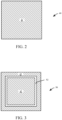
- FIG. 2 shows a plan view of an embodiment of a BGA package 40, in accordance with a manufacturing step of the present disclosure.
- FIG. 2 with continued reference to FIG. 1 shows a first layer 42 of a solder mask applied to a BGA substrate (e.g., a portion of the solder mask 26 of FIG. 1 ).
- FIG. 2 shows the first layer 42 of the solder mask applied to a top surface of the BGA substrate.
- the first layer may also be applied to a bottom surface (not shown) of the BGA substrate.
- FIG. 3 shows a plan view of an embodiment of a BGA package 50, in accordance with a manufacturing step of the present disclosure.
- FIG. 3 with continued reference to FIG. 2 shows a bonding area 52 exposed by removing part of the first layer 42 of the solder mask.
- the bonding area 52 is exposed by a photolithographic process.
- FIG. 4 shows a plan view of an embodiment of a BGA package 60, in accordance with a manufacturing step of the present disclosure.
- a second layer of the solder mask is applied to the first layer 52 to form a combined solder mask 54.
- FIG. 4 with continued reference to FIG. 3 shows the bonding area 52 exposed again while also forming (and then filling) a filled recessed portion 62 in the solder mask.
- the filled recessed portion 62 has a same depth as a thickness of the second layer.
- the depth of the filled recessed portion 62 is different than the thickness of second layer but less than the total thickness of the solder mask, including the first layer and second layer of the solder mask.
- a centerline 64 of the filled recessed portion 62 may align with a periphery of a die (not shown) to be affixed to the BGA package 60.
- FIG. 5 shows a cross-sectional view of a preceding manufacturing step to the embodiment of FIG. 4 taken along line A-A', in accordance with the present disclosure.
- the embodiment 70 of FIG. 5 includes a substrate core 72 and metallization 74 (e.g., copper interconnect), similar to the substrate core 18 and metallization 20 of FIG. 1 .
- a combined solder mask 54 is formed on a top surface of the embodiment 70. In one embodiment, the combined solder mask 54 is also formed on a bottom surface of the embodiment 70.
- the combined solder mask 54 includes a recessed portion 78 formed in the combined solder mask 54, prior to filling.
- the combined solder mask 54 includes the first layer 42 having a first thickness 80.
- the combined solder mask 54 including the application of the first layer 42 and the second layer has a combined thickness 82.
- FIG. 6 shows an embodiment 90 of a cross-sectional view of FIG. 4 taken along line A-A', in accordance with another manufacturing step of the present disclosure.
- FIG. 6 shows the filling of the recessed portion 78 with a dispenser 92, to form the filled recessed portion 62.
- the filled recessed portion 62 includes a same molding underfill, subsequently used to encapsulate the embodiment 90.
- the filled recessed portion 62 includes a different molding underfill, subsequently used to encapsulate the embodiment 90.
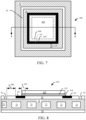
- FIG. 7 shows a plan view of an embodiment 100 of a BGA package, in accordance with another manufacturing step of the present disclosure.
- FIG. 7 shows a die 102 placed over the filled recessed portion 62.
- a periphery 104 of the die is preferably aligned to be coincident with the centerline 64 (illustrated in FIG. 4 ) of the filled recessed portion 62.
- the filled recessed portion 62 is formed with a minimum keep out distance 108 from the bonding area 52 to ensure adequate room is available for bonding a bonding wire to the bonding area 52.
- FIG. 8 shows an embodiment 110 of a cross-sectional view of FIG. 7 taken along line B-B', in accordance with another manufacturing step of the present disclosure.
- FIG. 8 shows the die 102 attached to the combined solder mask 54 with a die attach material 112.
- the die attach material 112 includes a bleed out area 114, where the die attach material 112 extrudes or bleeds out from under the die 102.
- the filled recessed portion 62 has a width to ensure a minimum keep out distance 108 from the bonding area 52.
- the width of the filled recessed portion 62 is further defined by a bleed out distance 116.
- the die 102 may be slightly misaligned with respect to the centerline 64 due to manufacturing tolerances, as long as the width of the filled recessed portion 62 is sufficient to satisfy the minimum required keep out distance 108 and minimum required bleed out distance 116.
- FIG. 9 shows a plan view of an embodiment 120 of a BGA package, in accordance with another manufacturing step of the present disclosure.
- a plurality of bond wires 122 electrically connect circuitry on the die 102 to bond fingers in the bond area 52.
- the bond fingers further connect to solder balls, similar to solder balls 24 of FIG. 1 , through the metallization 74 (see FIG. 8 ).
- FIG. 10 shows an embodiment 130 of a cross-sectional view of FIG. 9 taken along line C-C', in accordance with another manufacturing step of the present disclosure.
- the embodiment 130 shows a finalized BGA package, with attached solder balls 132 on a bottom surface of the BGA.
- the same molding underfill 134 used to fill the filled recessed portion 62 is used to encapsulate the BGA.
- a different molding underfill 134 used to fill the filled recessed portion 62 is used to encapsulate the BGA.
- the bonding area 52 may further include plating 136 to facilitate attaching bond wires 122 to the bond fingers in the bonding area 52.
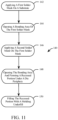
- FIG. 11 shows an embodiment 140 of a method to eliminate substrate metal cracks in a BGA, in accordance with an embodiment of the present disclosure.
- a first solder mask 42 (see FIG. 2 ) is applied to a substrate.
- a bonding area 52 is opened on the first solder mask 42, (see FIG. 3 ).
- a second solder mask is applied to the first solder mask, thereby forming a combined solder mask 54, (see FIG. 5 ).
- the bonding area 52 is reopened while forming a recessed portion 78 under a die periphery 104, (see FIG. 5 and FIG. 7 ).
- the recessed portion 78 is filled with a molding underfill to form a filled recessed portion 62, (see FIG. 6 ).
- an apparatus comprises a substrate comprising a planar surface.
- a die is attached to the planar surface of the substrate with an interposed die attach material.
- a solder mask is interposed between the die attach material and the planar surface, wherein the solder mask comprises a recessed portion extending beneath a periphery of the die, the recessed portion filled with a molding underfill.
- the solder mask comprises a first layer applied to the planar surface and a second layer applied on the first layer.
- the recessed portion comprises a depth equal to a thickness of the second layer.
- the recessed portion extends in a direction parallel to the planar surface and comprises a width greater than a bleed out distance of the die attach material. The width ensures the recessed portion is formed in the solder mask at least a minimum distance from a bond finger configured to bond with a wired connection to the die.
- the periphery of the die bisects the recessed portion.
- the die attach material comprises epoxy.
- the molding underfill filling the recessed portion is a same type of molding underfill used to encapsulate the die.
- the apparatus is a Ball Grid Array (BGA).
- the BGA is a Molded Array Process BGA.
- a method to eliminate substrate metal cracks in a ball grid array package comprises applying a first solder mask on a planar surface of a substrate. A bonding area of the first solder mask is opened to expose a bond finger configured to bond with a wired connection to a die. A second solder mask is applied on the first solder mask. The bonding area is opened to expose the bond finger and form a recessed portion under a periphery of the die. The recessed portion is filled with a molding underfill.
- Alternative embodiments of the method to eliminate substrate metal cracks in a ball grid array package include one of the following features, or any combination thereof.
- the die is attached to the second solder mask with a die attach material, wherein the periphery of the die bisects the recessed portion.
- the die is encapsulated with the molding underfill.
- a minimum width of the recessed portion is determined by a bleed out distance of the die attach material.
- a maximum width of the recessed portion is determined by defining a minimum distance of the recessed portion from a bond finger configured to bond with a wired connection to the die.
- an apparatus comprises a substrate comprising a first surface opposing a second surface, wherein the second surface comprises a plurality of solder balls arranged in a ball grid array.
- a die is attached to the first surface of the substrate with an interposed die attach material.
- a solder mask is interposed between the die attach material and the first surface, wherein the solder mask comprises a recessed portion extending beneath a periphery of the die, the recessed portion filled with a molding underfill used to encapsulate the die.
- the periphery of the die bisects the recessed portion.
- the recessed portion extends in a direction parallel to the planar surface and comprises a width greater than a bleed out distance of the die attach material.
- the width ensures the recessed portion is formed in the solder mask at least a minimum distance from a bond finger configured to bond with a wired connection to the die.
- the solder mask comprises a first layer applied to the first surface and a second layer applied on the first layer, wherein the recessed portion comprises a depth equal to a thickness of the second layer.
Landscapes
- Encapsulation Of And Coatings For Semiconductor Or Solid State Devices (AREA)
- Structures Or Materials For Encapsulating Or Coating Semiconductor Devices Or Solid State Devices (AREA)
- Engineering & Computer Science (AREA)
- Ceramic Engineering (AREA)
- Physics & Mathematics (AREA)
- Geometry (AREA)
Abstract
Description
- This disclosure relates generally to packaging of electronic components, and more specifically to the reduction of stress-induced cracks in a Ball Grid Array (BGA) package.
- Electronic component packaging includes the use of dissimilar materials, each with different temperature coefficients of expansion, thermal conductivity and the like. During component qualification and ultimately field operation, these various materials may expand and contract in ways that will introduce cracks leading to component failure. In particular, die attach epoxy may be used to attach a die (e.g., semiconductor die), to a substrate. The die attach epoxy will exhibit differential stress across the width of a die and expand or contract at a different rate to the die or substrate, when the package in temperature cycled. Such stress may lead to cracks forming in the epoxy, which may further lead to cracks in the substrate and electrical connections therein.
- The present invention is illustrated by way of example and is not limited by the accompanying figures, in which like references indicate similar elements. Elements in the figures are illustrated for simplicity and clarity and have not necessarily been drawn to scale.
-
FIG. 1 is a cross-sectional view of a BGA assembly, in accordance with an embodiment of the present disclosure. -
FIG. 2 is a plan view of an embodiment of a BGA package, in accordance with a manufacturing step of the present disclosure. -
FIG. 3 is a plan view of an embodiment of a BGA package, in accordance with another manufacturing step of the present disclosure. -
FIG. 4 is a plan view of an embodiment of a BGA package, in accordance with another manufacturing step of the present disclosure. -
FIG. 5 is a cross-sectional view of a preceding manufacturing step to the embodiment ofFIG. 4 taken along line A-A', in accordance with the present disclosure. -
FIG. 6 is a cross-sectional view of the embodiment ofFIG. 4 taken along line A-A', in accordance with another manufacturing step of the present disclosure. -
FIG. 7 is a plan view of an embodiment of a BGA package, in accordance with another manufacturing step of the present disclosure. -
FIG. 8 is a cross-sectional view of the embodiment ofFIG. 7 taken along line B-B', in accordance with another manufacturing step of the present disclosure. -
FIG. 9 is a plan view of an embodiment of a BGA package, in accordance with another manufacturing step of the present disclosure. -
FIG. 10 is a cross-sectional view of the embodiment ofFIG. 9 taken along line C-C', in accordance with another manufacturing step of the present disclosure. -
FIG. 11 is a flowchart representation of a method to eliminate substrate metal cracks in a BGA, in accordance with an embodiment of the present disclosure. - Embodiments described herein provide for the elimination, or substantial reduction, of substrate metal cracks in a BGA package as a result of die attach epoxy cracks propagating downward through the metallization patterns of the underlying substrate. Epoxy cracks due to thermal stress are prevented from propagating by forming a recessed portion beneath the die periphery and filling this portion with molding underfill.
-
FIG. 1 shows a cross-sectional view of aBGA package 10, in accordance with an embodiment of the present disclosure. The BGApackage 10 includes a die (e.g. a semiconductor die, a III/V compound die, a GaN die and the like), attached to a substrate 14 with a dieattach material 16. The substrate 14 further includes asubstrate core 18, a plurality of copper interconnect (or traces) 20 connected tovias 22 andsolder balls 24. Asolder mask 26 is applied to both sides of thesubstrate core 18. The die 12 is bonded withbond wires 28 to bond fingers 30 (shown with optional plating). Arecessed portion 32 is formed under the periphery of thedie 12 and filled with molding underfill. In one embodiment, a plan view of therecessed portion 32 follows the same shape as the periphery of the die 12. In another embodiment, therecessed portion 32 includes chamfered or rounded corners. -
FIG. 2 shows a plan view of an embodiment of aBGA package 40, in accordance with a manufacturing step of the present disclosure.FIG. 2 with continued reference toFIG. 1 shows afirst layer 42 of a solder mask applied to a BGA substrate (e.g., a portion of thesolder mask 26 ofFIG. 1 ).FIG. 2 shows thefirst layer 42 of the solder mask applied to a top surface of the BGA substrate. In one embodiment, the first layer may also be applied to a bottom surface (not shown) of the BGA substrate. -
FIG. 3 shows a plan view of an embodiment of aBGA package 50, in accordance with a manufacturing step of the present disclosure.FIG. 3 with continued reference toFIG. 2 shows abonding area 52 exposed by removing part of thefirst layer 42 of the solder mask. In one embodiment, thebonding area 52 is exposed by a photolithographic process. -
FIG. 4 shows a plan view of an embodiment of aBGA package 60, in accordance with a manufacturing step of the present disclosure. Subsequent to the exposure of thebonding area 52, a second layer of the solder mask is applied to thefirst layer 52 to form a combinedsolder mask 54.FIG. 4 with continued reference toFIG. 3 shows thebonding area 52 exposed again while also forming (and then filling) a filledrecessed portion 62 in the solder mask. In one embodiment, the filledrecessed portion 62 has a same depth as a thickness of the second layer. In another embodiment, the depth of the filledrecessed portion 62 is different than the thickness of second layer but less than the total thickness of the solder mask, including the first layer and second layer of the solder mask. In one embodiment, acenterline 64 of the filledrecessed portion 62 may align with a periphery of a die (not shown) to be affixed to theBGA package 60. -
FIG. 5 shows a cross-sectional view of a preceding manufacturing step to the embodiment ofFIG. 4 taken along line A-A', in accordance with the present disclosure. Theembodiment 70 ofFIG. 5 includes asubstrate core 72 and metallization 74 (e.g., copper interconnect), similar to thesubstrate core 18 andmetallization 20 ofFIG. 1 . A combinedsolder mask 54 is formed on a top surface of theembodiment 70. In one embodiment, the combinedsolder mask 54 is also formed on a bottom surface of theembodiment 70. The combinedsolder mask 54 includes a recessedportion 78 formed in the combinedsolder mask 54, prior to filling. The combinedsolder mask 54 includes thefirst layer 42 having afirst thickness 80. The combinedsolder mask 54 including the application of thefirst layer 42 and the second layer has a combinedthickness 82. -
FIG. 6 shows an embodiment 90 of a cross-sectional view ofFIG. 4 taken along line A-A', in accordance with another manufacturing step of the present disclosure.FIG. 6 , with continued reference toFIG. 4 and FIG. 5 shows the filling of therecessed portion 78 with adispenser 92, to form the filledrecessed portion 62. In one embodiment, the filledrecessed portion 62 includes a same molding underfill, subsequently used to encapsulate the embodiment 90. In another embodiment, the filledrecessed portion 62 includes a different molding underfill, subsequently used to encapsulate the embodiment 90. -
FIG. 7 shows a plan view of anembodiment 100 of a BGA package, in accordance with another manufacturing step of the present disclosure.FIG. 7 , with continued reference toFIG. 4 , shows a die 102 placed over the filledrecessed portion 62. In theembodiment 100, aperiphery 104 of the die is preferably aligned to be coincident with the centerline 64 (illustrated inFIG. 4 ) of the filledrecessed portion 62. In one embodiment, the filledrecessed portion 62 is formed with a minimum keep outdistance 108 from thebonding area 52 to ensure adequate room is available for bonding a bonding wire to thebonding area 52. -
FIG. 8 shows anembodiment 110 of a cross-sectional view ofFIG. 7 taken along line B-B', in accordance with another manufacturing step of the present disclosure.FIG. 8 , with continued reference toFIG. 6 andFIG. 7 shows the die 102 attached to the combinedsolder mask 54 with adie attach material 112. The dieattach material 112 includes a bleed outarea 114, where the dieattach material 112 extrudes or bleeds out from under the die 102. In one embodiment, the filledrecessed portion 62 has a width to ensure a minimum keep outdistance 108 from thebonding area 52. The width of the filled recessedportion 62 is further defined by a bleed outdistance 116. In another embodiment, thedie 102 may be slightly misaligned with respect to thecenterline 64 due to manufacturing tolerances, as long as the width of the filled recessedportion 62 is sufficient to satisfy the minimum required keep outdistance 108 and minimum required bleed outdistance 116. -
FIG. 9 shows a plan view of anembodiment 120 of a BGA package, in accordance with another manufacturing step of the present disclosure. In theembodiment 120, a plurality ofbond wires 122 electrically connect circuitry on thedie 102 to bond fingers in thebond area 52. The bond fingers further connect to solder balls, similar tosolder balls 24 ofFIG. 1 , through the metallization 74 (seeFIG. 8 ).FIG. 10 shows anembodiment 130 of a cross-sectional view ofFIG. 9 taken along line C-C', in accordance with another manufacturing step of the present disclosure. Theembodiment 130 shows a finalized BGA package, with attachedsolder balls 132 on a bottom surface of the BGA. In one embodiment, thesame molding underfill 134 used to fill the filled recessedportion 62 is used to encapsulate the BGA. In another embodiment, adifferent molding underfill 134 used to fill the filled recessedportion 62 is used to encapsulate the BGA. In another embodiment, thebonding area 52 may further include plating 136 to facilitate attachingbond wires 122 to the bond fingers in thebonding area 52. -
FIG. 11 shows anembodiment 140 of a method to eliminate substrate metal cracks in a BGA, in accordance with an embodiment of the present disclosure. With continued reference toFIG. 2, FIG. 3 ,FIG. 5, FIG. 6 andFIG. 7 , at 142 afirst solder mask 42, (seeFIG. 2 ) is applied to a substrate. At 144, abonding area 52 is opened on thefirst solder mask 42, (seeFIG. 3 ). At 146, a second solder mask is applied to the first solder mask, thereby forming a combinedsolder mask 54, (seeFIG. 5 ). At 148, thebonding area 52 is reopened while forming a recessedportion 78 under adie periphery 104, (seeFIG. 5 andFIG. 7 ). At 150, the recessedportion 78 is filled with a molding underfill to form a filled recessedportion 62, (seeFIG. 6 ). - As will be appreciated, at least some of the embodiments as disclosed include at least the following. In one embodiment, an apparatus comprises a substrate comprising a planar surface. A die is attached to the planar surface of the substrate with an interposed die attach material. A solder mask is interposed between the die attach material and the planar surface, wherein the solder mask comprises a recessed portion extending beneath a periphery of the die, the recessed portion filled with a molding underfill.
- Alternative embodiments of the apparatus include one of the following features, or any combination thereof. The solder mask comprises a first layer applied to the planar surface and a second layer applied on the first layer. The recessed portion comprises a depth equal to a thickness of the second layer. The recessed portion extends in a direction parallel to the planar surface and comprises a width greater than a bleed out distance of the die attach material. The width ensures the recessed portion is formed in the solder mask at least a minimum distance from a bond finger configured to bond with a wired connection to the die. The periphery of the die bisects the recessed portion. The die attach material comprises epoxy. The molding underfill filling the recessed portion is a same type of molding underfill used to encapsulate the die. The apparatus is a Ball Grid Array (BGA). The BGA is a Molded Array Process BGA.
- In another embodiment, a method to eliminate substrate metal cracks in a ball grid array package comprises applying a first solder mask on a planar surface of a substrate. A bonding area of the first solder mask is opened to expose a bond finger configured to bond with a wired connection to a die. A second solder mask is applied on the first solder mask. The bonding area is opened to expose the bond finger and form a recessed portion under a periphery of the die. The recessed portion is filled with a molding underfill.
- Alternative embodiments of the method to eliminate substrate metal cracks in a ball grid array package include one of the following features, or any combination thereof. The die is attached to the second solder mask with a die attach material, wherein the periphery of the die bisects the recessed portion. The die is encapsulated with the molding underfill. A minimum width of the recessed portion is determined by a bleed out distance of the die attach material. A maximum width of the recessed portion is determined by defining a minimum distance of the recessed portion from a bond finger configured to bond with a wired connection to the die.
- In another embodiment, an apparatus comprises a substrate comprising a first surface opposing a second surface, wherein the second surface comprises a plurality of solder balls arranged in a ball grid array. A die is attached to the first surface of the substrate with an interposed die attach material. A solder mask is interposed between the die attach material and the first surface, wherein the solder mask comprises a recessed portion extending beneath a periphery of the die, the recessed portion filled with a molding underfill used to encapsulate the die.
- Alternative embodiments of the apparatus include one of the following features, or any combination thereof. The periphery of the die bisects the recessed portion. The recessed portion extends in a direction parallel to the planar surface and comprises a width greater than a bleed out distance of the die attach material. The width ensures the recessed portion is formed in the solder mask at least a minimum distance from a bond finger configured to bond with a wired connection to the die. The solder mask comprises a first layer applied to the first surface and a second layer applied on the first layer, wherein the recessed portion comprises a depth equal to a thickness of the second layer.
- Although the invention is described herein with reference to specific embodiments, various modifications and changes can be made without departing from the scope of the present invention as set forth in the claims below. Accordingly, the specification and figures are to be regarded in an illustrative rather than a restrictive sense, and all such modifications are intended to be included within the scope of the present invention. Any benefits, advantages, or solutions to problems that are described herein with regard to specific embodiments are not intended to be construed as a critical, required, or essential feature or element of any or all the claims.
- Unless stated otherwise, terms such as "first" and "second" are used to arbitrarily distinguish between the elements such terms describe. Thus, these terms are not necessarily intended to indicate temporal or other prioritization of such elements.
Claims (15)
- An apparatus comprising:a substrate comprising a planar surface;a die attached to the planar surface of the substrate with an interposed die attach material; anda solder mask interposed between the die attach material and the planar surface, wherein the solder mask comprises a recessed portion extending beneath a periphery of the die, the recessed portion filled with a molding underfill.
- The apparatus of claim 1 wherein the solder mask comprises a first layer applied to the planar surface and a second layer applied on the first layer.
- The apparatus of claim 2 wherein the recessed portion comprises a depth equal to a thickness of the second layer.
- The apparatus of any preceding claim wherein the recessed portion extends in a direction parallel to the planar surface and comprises a width greater than a bleed out distance of the die attach material.
- The apparatus of claim 4 wherein the width ensures the recessed portion is formed in the solder mask at least a minimum distance from a bond finger configured to bond with a wired connection to the die.
- The apparatus of claim 4 or 5 wherein the periphery of the die bisects the recessed portion.
- The apparatus of any preceding claim wherein the die attach material comprises epoxy.
- The apparatus of any preceding claim wherein the molding underfill filling the recessed portion is a same type of molding underfill used to encapsulate the die.
- The apparatus of any preceding claim wherein the apparatus is a Ball Grid Array, BGA.
- The apparatus of claim 9 wherein the BGA is a Molded Array Process BGA.
- A method to eliminate substrate metal cracks in a ball grid array package comprising:applying a first solder mask on a planar surface of a substrate;opening a bonding area of the first solder mask to expose a bond finger configured to bond with a wired connection to a die;applying a second solder mask on the first solder mask;opening the bonding area to expose the bond finger and form a recessed portion under a periphery of the die; andfilling the recessed portion with a molding underfill.
- The method of claim 11 further comprising attaching the die to the second solder mask with a die attach material, wherein the periphery of the die bisects the recessed portion.
- The method of claim 11 or 12 further comprising encapsulating the die with the molding underfill.
- The method of any one of claims 11 to 13 further comprising determining a minimum width of the recessed portion by a bleed out distance of the die attach material.
- The method of any one of claims 11 to 14 further comprising determining a maximum width of the recessed portion by defining a minimum distance of the recessed portion from a bond finger configured to bond with a wired connection to the die.
Applications Claiming Priority (1)
| Application Number | Priority Date | Filing Date | Title |
|---|---|---|---|
| CN202211614334.9A CN118213329A (en) | 2022-12-15 | 2022-12-15 | Eliminating Substrate Metal Cracks in Ball Grid Array Packages |
Publications (2)
| Publication Number | Publication Date |
|---|---|
| EP4401125A2 true EP4401125A2 (en) | 2024-07-17 |
| EP4401125A3 EP4401125A3 (en) | 2024-08-14 |
Family
ID=89222218
Family Applications (1)
| Application Number | Title | Priority Date | Filing Date |
|---|---|---|---|
| EP23216202.4A Pending EP4401125A3 (en) | 2022-12-15 | 2023-12-13 | Eliminating substrate metal cracks in a ball grid array package |
Country Status (3)
| Country | Link |
|---|---|
| US (1) | US20240203905A1 (en) |
| EP (1) | EP4401125A3 (en) |
| CN (1) | CN118213329A (en) |
Family Cites Families (4)
| Publication number | Priority date | Publication date | Assignee | Title |
|---|---|---|---|---|
| US8982577B1 (en) * | 2012-02-17 | 2015-03-17 | Amkor Technology, Inc. | Electronic component package having bleed channel structure and method |
| US8803323B2 (en) * | 2012-06-29 | 2014-08-12 | Taiwan Semiconductor Manufacturing Company, Ltd. | Package structures and methods for forming the same |
| US9673150B2 (en) * | 2014-12-16 | 2017-06-06 | Nxp Usa, Inc. | EMI/RFI shielding for semiconductor device packages |
| TWI745162B (en) * | 2020-11-12 | 2021-11-01 | 力成科技股份有限公司 | Semiconductor package |
-
2022
- 2022-12-15 CN CN202211614334.9A patent/CN118213329A/en active Pending
-
2023
- 2023-10-02 US US18/479,144 patent/US20240203905A1/en active Pending
- 2023-12-13 EP EP23216202.4A patent/EP4401125A3/en active Pending
Also Published As
| Publication number | Publication date |
|---|---|
| US20240203905A1 (en) | 2024-06-20 |
| EP4401125A3 (en) | 2024-08-14 |
| CN118213329A (en) | 2024-06-18 |
Similar Documents
| Publication | Publication Date | Title |
|---|---|---|
| TWI437683B (en) | Packaged integrated circuit device having conductive through holes penetrating through body and manufacturing method thereof | |
| JP3063032B2 (en) | Ball grid array type semiconductor package and method of manufacturing the same | |
| US6124546A (en) | Integrated circuit chip package and method of making the same | |
| US6664615B1 (en) | Method and apparatus for lead-frame based grid array IC packaging | |
| US10109563B2 (en) | Modified leadframe design with adhesive overflow recesses | |
| US6262473B1 (en) | Film carrier tape and semiconductor device, method of making the same and circuit board | |
| US20080111224A1 (en) | Multi stack package and method of fabricating the same | |
| US20030218245A1 (en) | Semiconductor device and a method of manufacturing the same | |
| JP2006501677A (en) | Heat resistant package for block molded assemblies | |
| US20080199979A1 (en) | Semiconductor device and method for fabricating the same | |
| JP2009506572A (en) | Microfeature assemblies including interconnect structures and methods for forming such interconnect structures | |
| TW202541304A (en) | Electronic package structure | |
| JP2010010301A (en) | Semiconductor device and method of manufacturing the same | |
| CN106971985A (en) | Semiconductor packages and its manufacture method | |
| US7190066B2 (en) | Heat spreader and package structure utilizing the same | |
| US20120264257A1 (en) | Mold array process method to prevent exposure of substrate peripheries | |
| US6376916B1 (en) | Tape carrier for BGA and semiconductor device using the same | |
| US7432601B2 (en) | Semiconductor package and fabrication process thereof | |
| US11694950B2 (en) | Semiconductor package | |
| US20240203905A1 (en) | Eliminating substrate metal cracks in a ball grid array package | |
| US7572674B2 (en) | Method for manufacturing semiconductor device | |
| JP3226244B2 (en) | Resin-sealed semiconductor device | |
| CN112310028A (en) | Lead frame for packaging of semiconductor device, and process for manufacturing semiconductor device | |
| US20130256885A1 (en) | Copper Sphere Array Package | |
| JP2009182004A (en) | Semiconductor device |
Legal Events
| Date | Code | Title | Description |
|---|---|---|---|
| PUAI | Public reference made under article 153(3) epc to a published international application that has entered the european phase |
Free format text: ORIGINAL CODE: 0009012 |
|
| STAA | Information on the status of an ep patent application or granted ep patent |
Free format text: STATUS: THE APPLICATION HAS BEEN PUBLISHED |
|
| REG | Reference to a national code |
Ref country code: DE Ref legal event code: R079 Free format text: PREVIOUS MAIN CLASS: H01L0023130000 Ipc: G11C0005040000 |
|
| PUAL | Search report despatched |
Free format text: ORIGINAL CODE: 0009013 |
|
| AK | Designated contracting states |
Kind code of ref document: A2 Designated state(s): AL AT BE BG CH CY CZ DE DK EE ES FI FR GB GR HR HU IE IS IT LI LT LU LV MC ME MK MT NL NO PL PT RO RS SE SI SK SM TR |
|
| AK | Designated contracting states |
Kind code of ref document: A3 Designated state(s): AL AT BE BG CH CY CZ DE DK EE ES FI FR GB GR HR HU IE IS IT LI LT LU LV MC ME MK MT NL NO PL PT RO RS SE SI SK SM TR |
|
| RIC1 | Information provided on ipc code assigned before grant |
Ipc: H01L 23/498 20060101ALI20240710BHEP Ipc: H01L 23/31 20060101ALI20240710BHEP Ipc: H01L 23/13 20060101ALI20240710BHEP Ipc: G11C 5/04 20060101AFI20240710BHEP |
|
| STAA | Information on the status of an ep patent application or granted ep patent |
Free format text: STATUS: REQUEST FOR EXAMINATION WAS MADE |
|
| 17P | Request for examination filed |
Effective date: 20250214 |