EP4401123A1 - Device with isolation structures in active regions - Google Patents
Device with isolation structures in active regions Download PDFInfo
- Publication number
- EP4401123A1 EP4401123A1 EP23211353.0A EP23211353A EP4401123A1 EP 4401123 A1 EP4401123 A1 EP 4401123A1 EP 23211353 A EP23211353 A EP 23211353A EP 4401123 A1 EP4401123 A1 EP 4401123A1
- Authority
- EP
- European Patent Office
- Prior art keywords
- structures
- contacts
- gate structures
- active region
- gate
- Prior art date
- Legal status (The legal status is an assumption and is not a legal conclusion. Google has not performed a legal analysis and makes no representation as to the accuracy of the status listed.)
- Pending
Links
Images




Classifications
-
- H—ELECTRICITY
- H10—SEMICONDUCTOR DEVICES; ELECTRIC SOLID-STATE DEVICES NOT OTHERWISE PROVIDED FOR
- H10D—INORGANIC ELECTRIC SEMICONDUCTOR DEVICES
- H10D84/00—Integrated devices formed in or on semiconductor substrates that comprise only semiconducting layers, e.g. on Si wafers or on GaAs-on-Si wafers
- H10D84/80—Integrated devices formed in or on semiconductor substrates that comprise only semiconducting layers, e.g. on Si wafers or on GaAs-on-Si wafers characterised by the integration of at least one component covered by groups H10D12/00 or H10D30/00, e.g. integration of IGFETs
- H10D84/82—Integrated devices formed in or on semiconductor substrates that comprise only semiconducting layers, e.g. on Si wafers or on GaAs-on-Si wafers characterised by the integration of at least one component covered by groups H10D12/00 or H10D30/00, e.g. integration of IGFETs of only field-effect components
- H10D84/83—Integrated devices formed in or on semiconductor substrates that comprise only semiconducting layers, e.g. on Si wafers or on GaAs-on-Si wafers characterised by the integration of at least one component covered by groups H10D12/00 or H10D30/00, e.g. integration of IGFETs of only field-effect components of only insulated-gate FETs [IGFET]
- H10D84/85—Complementary IGFETs, e.g. CMOS
-
- H—ELECTRICITY
- H10—SEMICONDUCTOR DEVICES; ELECTRIC SOLID-STATE DEVICES NOT OTHERWISE PROVIDED FOR
- H10D—INORGANIC ELECTRIC SEMICONDUCTOR DEVICES
- H10D86/00—Integrated devices formed in or on insulating or conducting substrates, e.g. formed in silicon-on-insulator [SOI] substrates or on stainless steel or glass substrates
- H10D86/201—Integrated devices formed in or on insulating or conducting substrates, e.g. formed in silicon-on-insulator [SOI] substrates or on stainless steel or glass substrates the substrates comprising an insulating layer on a semiconductor body, e.g. SOI
-
- H—ELECTRICITY
- H10—SEMICONDUCTOR DEVICES; ELECTRIC SOLID-STATE DEVICES NOT OTHERWISE PROVIDED FOR
- H10D—INORGANIC ELECTRIC SEMICONDUCTOR DEVICES
- H10D84/00—Integrated devices formed in or on semiconductor substrates that comprise only semiconducting layers, e.g. on Si wafers or on GaAs-on-Si wafers
- H10D84/80—Integrated devices formed in or on semiconductor substrates that comprise only semiconducting layers, e.g. on Si wafers or on GaAs-on-Si wafers characterised by the integration of at least one component covered by groups H10D12/00 or H10D30/00, e.g. integration of IGFETs
- H10D84/82—Integrated devices formed in or on semiconductor substrates that comprise only semiconducting layers, e.g. on Si wafers or on GaAs-on-Si wafers characterised by the integration of at least one component covered by groups H10D12/00 or H10D30/00, e.g. integration of IGFETs of only field-effect components
- H10D84/83—Integrated devices formed in or on semiconductor substrates that comprise only semiconducting layers, e.g. on Si wafers or on GaAs-on-Si wafers characterised by the integration of at least one component covered by groups H10D12/00 or H10D30/00, e.g. integration of IGFETs of only field-effect components of only insulated-gate FETs [IGFET]
-
- H—ELECTRICITY
- H10—SEMICONDUCTOR DEVICES; ELECTRIC SOLID-STATE DEVICES NOT OTHERWISE PROVIDED FOR
- H10D—INORGANIC ELECTRIC SEMICONDUCTOR DEVICES
- H10D30/00—Field-effect transistors [FET]
- H10D30/60—Insulated-gate field-effect transistors [IGFET]
-
- H—ELECTRICITY
- H10—SEMICONDUCTOR DEVICES; ELECTRIC SOLID-STATE DEVICES NOT OTHERWISE PROVIDED FOR
- H10D—INORGANIC ELECTRIC SEMICONDUCTOR DEVICES
- H10D30/00—Field-effect transistors [FET]
- H10D30/60—Insulated-gate field-effect transistors [IGFET]
- H10D30/637—Lateral IGFETs having no inversion channels, e.g. buried channel lateral IGFETs, normally-on lateral IGFETs or depletion-mode lateral IGFETs
-
- H—ELECTRICITY
- H10—SEMICONDUCTOR DEVICES; ELECTRIC SOLID-STATE DEVICES NOT OTHERWISE PROVIDED FOR
- H10D—INORGANIC ELECTRIC SEMICONDUCTOR DEVICES
- H10D62/00—Semiconductor bodies, or regions thereof, of devices having potential barriers
- H10D62/10—Shapes, relative sizes or dispositions of the regions of the semiconductor bodies; Shapes of the semiconductor bodies
- H10D62/113—Isolations within a component, i.e. internal isolations
- H10D62/115—Dielectric isolations, e.g. air gaps
-
- H—ELECTRICITY
- H10—SEMICONDUCTOR DEVICES; ELECTRIC SOLID-STATE DEVICES NOT OTHERWISE PROVIDED FOR
- H10D—INORGANIC ELECTRIC SEMICONDUCTOR DEVICES
- H10D62/00—Semiconductor bodies, or regions thereof, of devices having potential barriers
- H10D62/10—Shapes, relative sizes or dispositions of the regions of the semiconductor bodies; Shapes of the semiconductor bodies
- H10D62/113—Isolations within a component, i.e. internal isolations
- H10D62/115—Dielectric isolations, e.g. air gaps
- H10D62/116—Dielectric isolations, e.g. air gaps adjoining the input or output regions of field-effect devices, e.g. adjoining source or drain regions
-
- H—ELECTRICITY
- H10—SEMICONDUCTOR DEVICES; ELECTRIC SOLID-STATE DEVICES NOT OTHERWISE PROVIDED FOR
- H10D—INORGANIC ELECTRIC SEMICONDUCTOR DEVICES
- H10D84/00—Integrated devices formed in or on semiconductor substrates that comprise only semiconducting layers, e.g. on Si wafers or on GaAs-on-Si wafers
- H10D84/01—Manufacture or treatment
- H10D84/0123—Integrating together multiple components covered by H10D12/00 or H10D30/00, e.g. integrating multiple IGBTs
- H10D84/0126—Integrating together multiple components covered by H10D12/00 or H10D30/00, e.g. integrating multiple IGBTs the components including insulated gates, e.g. IGFETs
- H10D84/0149—Manufacturing their interconnections or electrodes, e.g. source or drain electrodes
-
- H—ELECTRICITY
- H10—SEMICONDUCTOR DEVICES; ELECTRIC SOLID-STATE DEVICES NOT OTHERWISE PROVIDED FOR
- H10D—INORGANIC ELECTRIC SEMICONDUCTOR DEVICES
- H10D84/00—Integrated devices formed in or on semiconductor substrates that comprise only semiconducting layers, e.g. on Si wafers or on GaAs-on-Si wafers
- H10D84/01—Manufacture or treatment
- H10D84/0123—Integrating together multiple components covered by H10D12/00 or H10D30/00, e.g. integrating multiple IGBTs
- H10D84/0126—Integrating together multiple components covered by H10D12/00 or H10D30/00, e.g. integrating multiple IGBTs the components including insulated gates, e.g. IGFETs
- H10D84/0165—Integrating together multiple components covered by H10D12/00 or H10D30/00, e.g. integrating multiple IGBTs the components including insulated gates, e.g. IGFETs the components including complementary IGFETs, e.g. CMOS devices
- H10D84/017—Manufacturing their source or drain regions, e.g. silicided source or drain regions
-
- H—ELECTRICITY
- H10—SEMICONDUCTOR DEVICES; ELECTRIC SOLID-STATE DEVICES NOT OTHERWISE PROVIDED FOR
- H10D—INORGANIC ELECTRIC SEMICONDUCTOR DEVICES
- H10D84/00—Integrated devices formed in or on semiconductor substrates that comprise only semiconducting layers, e.g. on Si wafers or on GaAs-on-Si wafers
- H10D84/01—Manufacture or treatment
- H10D84/0123—Integrating together multiple components covered by H10D12/00 or H10D30/00, e.g. integrating multiple IGBTs
- H10D84/0126—Integrating together multiple components covered by H10D12/00 or H10D30/00, e.g. integrating multiple IGBTs the components including insulated gates, e.g. IGFETs
- H10D84/0165—Integrating together multiple components covered by H10D12/00 or H10D30/00, e.g. integrating multiple IGBTs the components including insulated gates, e.g. IGFETs the components including complementary IGFETs, e.g. CMOS devices
- H10D84/0186—Manufacturing their interconnections or electrodes, e.g. source or drain electrodes
-
- H—ELECTRICITY
- H10—SEMICONDUCTOR DEVICES; ELECTRIC SOLID-STATE DEVICES NOT OTHERWISE PROVIDED FOR
- H10D—INORGANIC ELECTRIC SEMICONDUCTOR DEVICES
- H10D84/00—Integrated devices formed in or on semiconductor substrates that comprise only semiconducting layers, e.g. on Si wafers or on GaAs-on-Si wafers
- H10D84/01—Manufacture or treatment
- H10D84/0123—Integrating together multiple components covered by H10D12/00 or H10D30/00, e.g. integrating multiple IGBTs
- H10D84/0126—Integrating together multiple components covered by H10D12/00 or H10D30/00, e.g. integrating multiple IGBTs the components including insulated gates, e.g. IGFETs
- H10D84/0165—Integrating together multiple components covered by H10D12/00 or H10D30/00, e.g. integrating multiple IGBTs the components including insulated gates, e.g. IGFETs the components including complementary IGFETs, e.g. CMOS devices
- H10D84/0188—Manufacturing their isolation regions
-
- H—ELECTRICITY
- H10—SEMICONDUCTOR DEVICES; ELECTRIC SOLID-STATE DEVICES NOT OTHERWISE PROVIDED FOR
- H10D—INORGANIC ELECTRIC SEMICONDUCTOR DEVICES
- H10D84/00—Integrated devices formed in or on semiconductor substrates that comprise only semiconducting layers, e.g. on Si wafers or on GaAs-on-Si wafers
- H10D84/01—Manufacture or treatment
- H10D84/02—Manufacture or treatment characterised by using material-based technologies
- H10D84/03—Manufacture or treatment characterised by using material-based technologies using Group IV technology, e.g. silicon technology or silicon-carbide [SiC] technology
- H10D84/038—Manufacture or treatment characterised by using material-based technologies using Group IV technology, e.g. silicon technology or silicon-carbide [SiC] technology using silicon technology, e.g. SiGe
-
- H—ELECTRICITY
- H10—SEMICONDUCTOR DEVICES; ELECTRIC SOLID-STATE DEVICES NOT OTHERWISE PROVIDED FOR
- H10D—INORGANIC ELECTRIC SEMICONDUCTOR DEVICES
- H10D86/00—Integrated devices formed in or on insulating or conducting substrates, e.g. formed in silicon-on-insulator [SOI] substrates or on stainless steel or glass substrates
- H10D86/01—Manufacture or treatment
-
- H—ELECTRICITY
- H10—SEMICONDUCTOR DEVICES; ELECTRIC SOLID-STATE DEVICES NOT OTHERWISE PROVIDED FOR
- H10W—GENERIC PACKAGES, INTERCONNECTIONS, CONNECTORS OR OTHER CONSTRUCTIONAL DETAILS OF DEVICES COVERED BY CLASS H10
- H10W10/00—Isolation regions in semiconductor bodies between components of integrated devices
- H10W10/01—Manufacture or treatment
- H10W10/011—Manufacture or treatment of isolation regions comprising dielectric materials
- H10W10/014—Manufacture or treatment of isolation regions comprising dielectric materials using trench refilling with dielectric materials, e.g. shallow trench isolations
-
- H—ELECTRICITY
- H10—SEMICONDUCTOR DEVICES; ELECTRIC SOLID-STATE DEVICES NOT OTHERWISE PROVIDED FOR
- H10W—GENERIC PACKAGES, INTERCONNECTIONS, CONNECTORS OR OTHER CONSTRUCTIONAL DETAILS OF DEVICES COVERED BY CLASS H10
- H10W10/00—Isolation regions in semiconductor bodies between components of integrated devices
- H10W10/10—Isolation regions comprising dielectric materials
- H10W10/17—Isolation regions comprising dielectric materials formed using trench refilling with dielectric materials, e.g. shallow trench isolations
-
- H—ELECTRICITY
- H10—SEMICONDUCTOR DEVICES; ELECTRIC SOLID-STATE DEVICES NOT OTHERWISE PROVIDED FOR
- H10W—GENERIC PACKAGES, INTERCONNECTIONS, CONNECTORS OR OTHER CONSTRUCTIONAL DETAILS OF DEVICES COVERED BY CLASS H10
- H10W20/00—Interconnections in chips, wafers or substrates
- H10W20/20—Interconnections within wafers or substrates, e.g. through-silicon vias [TSV]
-
- H—ELECTRICITY
- H10—SEMICONDUCTOR DEVICES; ELECTRIC SOLID-STATE DEVICES NOT OTHERWISE PROVIDED FOR
- H10D—INORGANIC ELECTRIC SEMICONDUCTOR DEVICES
- H10D30/00—Field-effect transistors [FET]
- H10D30/01—Manufacture or treatment
- H10D30/021—Manufacture or treatment of FETs having insulated gates [IGFET]
- H10D30/027—Manufacture or treatment of FETs having insulated gates [IGFET] of lateral single-gate IGFETs
- H10D30/0275—Manufacture or treatment of FETs having insulated gates [IGFET] of lateral single-gate IGFETs forming single crystalline semiconductor source or drain regions resulting in recessed gates, e.g. forming raised source or drain regions
-
- H—ELECTRICITY
- H10—SEMICONDUCTOR DEVICES; ELECTRIC SOLID-STATE DEVICES NOT OTHERWISE PROVIDED FOR
- H10D—INORGANIC ELECTRIC SEMICONDUCTOR DEVICES
- H10D30/00—Field-effect transistors [FET]
- H10D30/60—Insulated-gate field-effect transistors [IGFET]
- H10D30/791—Arrangements for exerting mechanical stress on the crystal lattice of the channel regions
- H10D30/797—Arrangements for exerting mechanical stress on the crystal lattice of the channel regions being in source or drain regions, e.g. SiGe source or drain
-
- H—ELECTRICITY
- H10—SEMICONDUCTOR DEVICES; ELECTRIC SOLID-STATE DEVICES NOT OTHERWISE PROVIDED FOR
- H10D—INORGANIC ELECTRIC SEMICONDUCTOR DEVICES
- H10D62/00—Semiconductor bodies, or regions thereof, of devices having potential barriers
- H10D62/80—Semiconductor bodies, or regions thereof, of devices having potential barriers characterised by the materials
- H10D62/82—Heterojunctions
-
- H—ELECTRICITY
- H10—SEMICONDUCTOR DEVICES; ELECTRIC SOLID-STATE DEVICES NOT OTHERWISE PROVIDED FOR
- H10D—INORGANIC ELECTRIC SEMICONDUCTOR DEVICES
- H10D62/00—Semiconductor bodies, or regions thereof, of devices having potential barriers
- H10D62/80—Semiconductor bodies, or regions thereof, of devices having potential barriers characterised by the materials
- H10D62/82—Heterojunctions
- H10D62/822—Heterojunctions comprising only Group IV materials heterojunctions, e.g. Si/Ge heterojunctions
-
- H—ELECTRICITY
- H10—SEMICONDUCTOR DEVICES; ELECTRIC SOLID-STATE DEVICES NOT OTHERWISE PROVIDED FOR
- H10D—INORGANIC ELECTRIC SEMICONDUCTOR DEVICES
- H10D64/00—Electrodes of devices having potential barriers
- H10D64/20—Electrodes characterised by their shapes, relative sizes or dispositions
- H10D64/23—Electrodes carrying the current to be rectified, amplified, oscillated or switched, e.g. sources, drains, anodes or cathodes
- H10D64/251—Source or drain electrodes for field-effect devices
- H10D64/257—Source or drain electrodes for field-effect devices for lateral devices wherein the source or drain electrodes are characterised by top-view geometrical layouts, e.g. interdigitated, semi-circular, annular or L-shaped electrodes
-
- H—ELECTRICITY
- H10—SEMICONDUCTOR DEVICES; ELECTRIC SOLID-STATE DEVICES NOT OTHERWISE PROVIDED FOR
- H10D—INORGANIC ELECTRIC SEMICONDUCTOR DEVICES
- H10D84/00—Integrated devices formed in or on semiconductor substrates that comprise only semiconducting layers, e.g. on Si wafers or on GaAs-on-Si wafers
- H10D84/01—Manufacture or treatment
- H10D84/0123—Integrating together multiple components covered by H10D12/00 or H10D30/00, e.g. integrating multiple IGBTs
- H10D84/0126—Integrating together multiple components covered by H10D12/00 or H10D30/00, e.g. integrating multiple IGBTs the components including insulated gates, e.g. IGFETs
- H10D84/0135—Manufacturing their gate conductors
-
- H—ELECTRICITY
- H10—SEMICONDUCTOR DEVICES; ELECTRIC SOLID-STATE DEVICES NOT OTHERWISE PROVIDED FOR
- H10D—INORGANIC ELECTRIC SEMICONDUCTOR DEVICES
- H10D84/00—Integrated devices formed in or on semiconductor substrates that comprise only semiconducting layers, e.g. on Si wafers or on GaAs-on-Si wafers
- H10D84/01—Manufacture or treatment
- H10D84/0123—Integrating together multiple components covered by H10D12/00 or H10D30/00, e.g. integrating multiple IGBTs
- H10D84/0126—Integrating together multiple components covered by H10D12/00 or H10D30/00, e.g. integrating multiple IGBTs the components including insulated gates, e.g. IGFETs
- H10D84/0151—Manufacturing their isolation regions
-
- H—ELECTRICITY
- H10—SEMICONDUCTOR DEVICES; ELECTRIC SOLID-STATE DEVICES NOT OTHERWISE PROVIDED FOR
- H10D—INORGANIC ELECTRIC SEMICONDUCTOR DEVICES
- H10D89/00—Aspects of integrated devices not covered by groups H10D84/00 - H10D88/00
- H10D89/10—Integrated device layouts
Definitions
- the present disclosure relates to semiconductor structures and, more particularly, to devices with isolation structures in active regions and methods of manufacture.
- COAG Contact Over Active Gate
- a structure comprises: an active region; a plurality of isolation structures within the active region; a plurality of gate structures overlapping the plurality of isolation structures within the active region; and diffusion regions on sides of the plurality of gate structures and the plurality of isolation structures. Additional features of the structure are set forth in dependent claims 2 to 8.
- a structure comprises: at least one active region; a plurality of isolation structures within the at least one active region; a plurality of gate structures overlapping the plurality of isolation structures within the at least one active region; raised source/drain regions on sides of the plurality of gate structures and the plurality of isolation structures; a first set of contacts to the raised source/drain regions; and a second set of contacts to the plurality of gate structures. Additional features of the structure are set forth in dependent claims 10 to 14.
- a method comprises: forming a plurality of isolation structures within an active region; forming a plurality of gate structures overlapping the plurality of isolation structures within the active region; forming diffusion regions on sides of the plurality of gate structures and the plurality of isolation structures; and forming contacts to the diffusion regions and the plurality of gate structures.
- the present disclosure relates to semiconductor structures and, more particularly, to devices with isolation structures in active regions and methods of manufacture. More specifically, the present disclosure relates to a high performance radio frequency (RF) device with embedded shallow trench isolation structures in an active region.
- the shallow trench isolation structures e.g., islands
- RX active region
- the shallow trench isolation structures may be enclosed on all sides by the active region.
- the present disclosure provides a large width very short channel high performance RF device (high FT/Fmax), with a compact design (e.g., with a same footprint as a conventional Contact over Active Gate Process (COAG) RF multi-finger design).
- a compact design e.g., with a same footprint as a conventional Contact over Active Gate Process (COAG) RF multi-finger design.
- COAG Contact over Active Gate Process
- the present disclosure maintains and/or improves FT of a wide device while improving Fmax.
- the device does not exhibit shorting between a raised source/drain (S/D) and the active gate structure.
- the processes for fabricating the devices are easily integrated with existing process flows with no additional masking steps.
- the devices of the present disclosure can be manufactured in a number of ways using a number of different tools.
- the methodologies and tools are used to form structures with dimensions in the micrometer and nanometer scale.
- the methodologies, i.e., technologies, employed to manufacture the devices of the present disclosure have been adopted from integrated circuit (IC) technology.
- the structures are built on wafers and are realized in films of material patterned by photolithographic processes on the top of a wafer.
- the fabrication of the devices uses three basic building blocks: (i) deposition of thin films of material on a substrate, (ii) applying a patterned mask on top of the films by photolithographic imaging, and (iii) etching the films selectively to the mask.
- precleaning processes may be used to clean etched surfaces of any contaminants, as is known in the art.
- rapid thermal anneal processes may be used to drive-in dopants or material layers as is known in the art.
- FIG. 1A shows a top view of a device in accordance with aspects of the present disclosure.
- FIG. 1B shows a cross-sectional view of the device of FIG. 1 along line A-A; whereas FIG. 1C shows a cross-sectional view of the device of FIG. 1 along line B-B.
- the device 10 shown in FIGS. 1A-1C may be a multi-finger fully depleted semiconductor on insulator (FDSOI) MOSFET on a single diffusion region.
- FDSOI fully depleted semiconductor on insulator
- the device 10 includes a semiconductor substrate 12.
- the semiconductor substrate 12 includes a handle substrate 12a, a buried insulator layer 12b on the handle substrate 12a and a top layer of semiconductor material 12c.
- the handle substrate 12a provides mechanical support to the buried insulator layer 12b and the top semiconductor layer 12c.
- the handle substrate 12a and top semiconductor material 12c may be composed of any suitable material including, but not limited to, Si, SiGe, SiGeC, SiC, alloys, GaAs, InAs, InP, and other III/V or II/VI compound semiconductors.
- the handle substrate 12a and the top semiconductor layer 12c comprise a single crystalline semiconductor material, such as, for example, single crystalline silicon.
- the handle substrate 12a and the top semiconductor layer 12c may also comprise any suitable crystallographic orientation (e.g., a (100), (110), (111), or (001) crystallographic orientation).
- the buried insulator layer 12b comprises any suitable material, including silicon oxide, sapphire, other suitable insulating materials, and/or combinations thereof.
- An exemplary insulator layer 12b may be a buried oxide layer (BOX).
- Shallow trench isolation structures 14 may be formed in the semiconductor substrate 12, e.g., extending to the buried insulator layer 12b.
- the shallow trench isolation structures 14 may be separate islands embedded within the active region, e.g., top semiconductor layer 12c.
- the shallow trench isolation structures 14 can also be deep trench isolation structures.
- the shallow trench isolation structures 14 e.g., islands of the shallow trench isolation structures 14
- the shallow trench isolation structures 14 are under gate structures 16 and are enclosed on all sides with the active region, e.g., top semiconductor material 12c.
- the shallow trench isolation structures 14 may provide a stress enhancement on the channel of the gate structures 16.
- the gate structures 16 may be formed over the shallow trench isolation structures 14 and the active regions, e.g., top semiconductor layer 12c. In embodiments, the gate structures 16 may overlap and be centered over the shallow trench isolation structures 14. The gate structures 16 can be implemented in a minimum gate length according to design rules. In embodiments, the shallow trench isolation structures 14 will prevent shorting between raised diffusion regions (e.g., source and drain regions) 18 and the gate structures 16, e.g., contacts 20b of the gate structures 16 and contacts 20a of raised source and drain regions 18. Also, by having the gate structures 16 over the shallow trench isolation structures 14 and the active regions, e.g., top semiconductor layer 12c, device electrical characteristics show high FT/high Fmax at a wide active region.
- raised diffusion regions e.g., source and drain regions
- the gate structures 16 include a gate dielectric material 16a, a gate electrode 16b, and sidewall spacers 16c.
- the gate dielectric material 16a may be a high-k dielectric material or a low-k dielectric material.
- the high-k dielectric material may be, e.g., HfO 2 Al 2 O 3 , Ta 2 O 3 , TiO 2 , La 2 O 3 , SrTiO 3 , LaAlO 3 , ZrO 2 , Y 2 O 3 , Gd 2 O 3 , and combinations including multilayers thereof.
- the gate electrode 16b may be a polysilicon material or a replacement metal gate material as is known in the art, e.g., Ti, TiAlC, Al, TiAl, TaN, TiN, TiC, Co, etc.
- the sidewall spacers 16c may comprise nitride and/or oxide.
- the gate structures 16 can be fabricated using conventional CMOS processes.
- the gate structures 16 can be fabricated using standard CMOS or replacement gate processes.
- CMOS processing as further described herein, a gate dielectric and polysilicon are formed, e.g., deposited, on the top semiconductor layer 12c, followed a patterning process.
- An insulator material such as nitride or oxide can be deposited on the patterned materials, followed by an anisotropic etching process to form the sidewall spacers 16c.
- FIGS. 1A-1C further show source/drain regions 18 formed on the top semiconductor layer 12c between the gate structures 16.
- the source/drain regions 18 may be raised epitaxy regions formed by selectively growing a semiconductor material on the top semiconductor layer 12c.
- Contacts 20a, 20b may be formed on the gate electrode 16b and the source/drain regions 18.
- Wiring structures 24a, 24b may be formed in contact with the respective contacts 20a, 20b.
- the wiring structures 24b may be aligned with the gate structures 16 (e.g., parallel with the gate structures 16); whereas the wiring structures 24a may be aligned with the contacts 20a over the source/drain regions 18. Accordingly, in embodiments, the contacts 20a may be formed to the source/drain regions 18 and the contacts 20b may be formed to the gate electrode 16b, landing over the shallow trench isolation structures 14.
- the contacts 20a, 20b and wiring structures 24a, 24b may be formed by conventional lithography, etching and deposition processes, by forming a trench in an interlevel dielectric material 22 to expose the underlying gate electrode 16b and the source/drain regions 18, followed by a deposition process of a conductive material.
- the conducive material may be Al or Tungsten, as examples.
- the contacts 20b formed on the gate electrode 16b and the contacts 20a formed on the source/drain regions 18 may be staggered, e.g., not aligned with one another.
- the contacts 20b on the gate electrodes 16b are aligned over the shallow trench isolation structures 16.
- a silicide process may be performed on the exposed gate electrode 16b and the source/drain regions 18.
- the silicide process begins with deposition of a thin transition metal layer, e.g., nickel, cobalt or titanium, over fully formed raised source/drain regions 18 and gate electrode 16b. After deposition of the material, the structure is heated allowing the transition metal to react with exposed silicon (or other semiconductor material as described herein) in the active regions of the semiconductor device (e.g., raised source/drain regions 18 and gate electrode 16b) forming a low-resistance transition metal silicide.
- a thin transition metal layer e.g., nickel, cobalt or titanium
- any remaining transition metal is removed by chemical etching, leaving silicide contacts in the active regions of the device. It should be understood by those of skill in the art that silicide contacts will not be required on the devices, when a gate structure is composed of a metal material.
- FIG. 2 shows a top view of a device in accordance with additional aspects of the present disclosure.
- multiple active regions 12x are shown, each separated by a respective isolation structure 26.
- the isolation structure 26 may be a shallow trench isolation structure or a deep trench isolation structure.
- the multiple active regions 12x may be separated by a minimum distance allowed by design rules.
- the gate structures 16 extend over the multiple active regions 12x, and each of the active regions 12x include the shallow trench isolation structures 14 embedded within the active region 12x and aligned with (overlapping) the gate structures 16.
- the remaining features of the device 10a of FIG. 2 are similar to the device 10 described with respect to FIGS. 1A-1C .
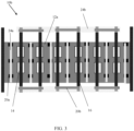
- FIG. 3 shows a top view of a device in accordance with further aspects of the present disclosure.
- the contacts 20b for the gate structures 16 are provided above and below the active region 12a. That is, the contacts 20b may be placed beyond the active region 12a on opposite edges of gate structures 16 before termination of the gate structures 16. In this way, the contacts 20b for the gate structures 16 are perpendicular to the gate structures 16 and are not provided on or aligned with the shallow trench isolation structures 14.
- the wiring structures 24b extend over the multiple contacts 20b for the gate structures 16, e.g., parallel and aligned with the contacts 20b for the gate structures 16.
- the shallow trench isolation structures 14 may be deep trench isolation structures extending through the buried insulator layer 12b. The remaining features of the device 10b of FIG. 3 are similar to the device 10 described with respect to FIGS. 1A-1C .
- FIG. 4 shows a top view of a device in accordance with additional aspects of the present disclosure.
- multiple active regions 12x are shown, each separated by the isolation structure 26.
- the multiple active regions 12x may be separated by a minimum distance allowed by design rules as already described herein.
- the gate structures 16 extend over the multiple active regions 12x, and each of the active regions 12x includes the shallow trench isolation structures 14 embedded within the active region 12x and aligned with the gate structures 16.
- the contacts 20b for the gate structures 16 are provided above and below each of the active regions 12x. That is, similar to that shown in FIG. 3 , the contacts 20b may be placed beyond the active regions 12x.
- the contacts 20b for the gate structures 16 are perpendicular to the gate structures 16 and are not provided on or aligned with the shallow trench isolation structures 14.
- the wiring structures 24b extend over the multiple contacts 20b for the gate structures 16, e.g., parallel and aligned with the contacts 20b for the gate structures 16.
- the remaining features of the device 10c of FIG. 4 are similar to the device 10b described with respect to FIG. 3 .
- FIGS. 5A-5C show fabrication processes of manufacturing the device 10 of FIGS. 1A-1C .
- shallow trench isolation structures 14 are formed in the substrate 12.
- the shallow trench isolation structures 14 can be formed by conventional lithography, etching and deposition methods known to those of skill in the art. For example, a resist formed over the top semiconductor layer 12c is exposed to energy (light) and developed utilizing a conventional resist developer to form a pattern (opening).
- etching process with a selective chemistry, e.g., reactive ion etching (RIE), will be used to transfer the pattern from the photoresist layer to the top semiconductor layer 12c to form one or more trenches in the top semiconductor layer 12c and extending into the buried insulator layer 12b through the openings of the resist.
- the insulator material e.g., SiO 2
- CVD chemical vapor deposition
- Any residual material on the surface of the top semiconductor layer 12c can be removed by conventional chemical mechanical polishing (CMP) processes. This process can also be used to form deep trench isolation structures.
- the gate structures 16 are formed over the shallow trench isolation structures 14.
- the gate structures 16 can be formed by depositing the gate dielectric material 16a over the shallow trench isolation structures 16 and the active regions, e.g., top semiconductor layer 12c.
- the gate dielectric material 16a may be blanket deposited using CVD, Plasma Enhanced CVD (PECVD) or atomic layer deposition (ALD), as examples.
- the gate electrode 16b e.g., polysilicon, may be blanket deposited over the gate dielectric material 16a using a conventional CVD process.
- the gate dielectric material 16a and the gate electrode 16b may be patterned using conventional lithography and etching processes as described herein.
- the sidewall spacers 16c may be formed by a deposition (e.g., CVD) of nitride and/or oxide, followed by an anisotropic etching process.
- the source/drain regions 18 may be formed on the active regions, e.g., top semiconductor layer 12c.
- the source/drain regions 18 may be raised epitaxy regions comprising SiGe or Si as examples.
- the epitaxy regions may be formed of a III-V compound semiconductor such as GaAs, InP, GaN, InGaAs, InAlAs, GaSb, AlSb, AlAs, AlP, GaP, combinations thereof, or multilayers thereof.
- a p-type or an n-type impurity may be in-situ doped.
- silicon germanium boron (SiGeB) may be grown.
- silicon phosphorous (SiP) or silicon carbon phosphorous (SiCP) may be grown.
- FIGS. 1A-1C show the fabrication of the contacts 20a, 20b and wiring structures 24a, 24b, as already described herein.
- SoC system on chip
- the devices can be utilized in system on chip (SoC) technology.
- SoC is an integrated circuit (also known as a "chip") that integrates all components of an electronic system on a single chip or substrate. As the components are integrated on a single substrate, SoCs consume much less power and take up much less area than multichip designs with equivalent functionality. Because of this, SoCs are becoming the dominant force in the mobile computing (such as in Smartphones) and edge computing markets. SoC is also used in embedded systems and the Internet of Things.
- the method(s) as described above is used in the fabrication of integrated circuit chips.
- the resulting integrated circuit chips can be distributed by the fabricator in raw wafer form (that is, as a single wafer that has multiple unpackaged chips), as a bare die, or in a packaged form.
- the chip is mounted in a single chip package (such as a plastic carrier, with leads that are affixed to a motherboard or other higher level carrier) or in a multichip package (such as a ceramic carrier that has either or both surface interconnections or buried interconnections).
- the chip is then integrated with other chips, discrete circuit elements, and/or other signal processing devices as part of either (a) an intermediate product, such as a motherboard, or (b) an end product.
- the end product can be any product that includes integrated circuit chips, ranging from toys and other low-end applications to advanced computer products having a display, a keyboard or other input device, and a central processor.
Landscapes
- Insulated Gate Type Field-Effect Transistor (AREA)
- Thin Film Transistor (AREA)
Abstract
Description
- The present disclosure relates to semiconductor structures and, more particularly, to devices with isolation structures in active regions and methods of manufacture.
- Contact Over Active Gate (COAG) is an enhanced semiconductor process flow technique that removes the need for the gate contact to land at the end-to-end spacing region between the nMOS and pMOS devices. COAG is used to enable aggressive scaling of the standard cell height by moving the gate contact over the active gate region, thereby reducing the space region between the end of the nMOS and the end of the pMOS devices.
- However, there are limitations posed by the COAG. These limitations are posed by a minimum channel length that can be supported for reliable contact. For example, with minimum channel length, the contact to the active gate and the contact to the source/drain region may contact resulting in a shorting of the device. To address this issue, channel length may be widened. This presents additional issues with respect to Fmax and FT. For example, there is a known inverse relationship between the Fmax and FT such that widening the active regions may improve Fmax, but will also negatively affect FT.
- In an aspect of the disclosure, a structure comprises: an active region; a plurality of isolation structures within the active region; a plurality of gate structures overlapping the plurality of isolation structures within the active region; and diffusion regions on sides of the plurality of gate structures and the plurality of isolation structures.
Additional features of the structure are set forth in dependent claims 2 to 8. - In an aspect of the disclosure, a structure comprises: at least one active region; a plurality of isolation structures within the at least one active region; a plurality of gate structures overlapping the plurality of isolation structures within the at least one active region; raised source/drain regions on sides of the plurality of gate structures and the plurality of isolation structures; a first set of contacts to the raised source/drain regions; and a second set of contacts to the plurality of gate structures.
Additional features of the structure are set forth independent claims 10 to 14. - In an aspect of the disclosure, a method comprises: forming a plurality of isolation structures within an active region; forming a plurality of gate structures overlapping the plurality of isolation structures within the active region; forming diffusion regions on sides of the plurality of gate structures and the plurality of isolation structures; and forming contacts to the diffusion regions and the plurality of gate structures.
- The present disclosure is described in the detailed description which follows, in reference to the noted plurality of drawings by way of non-limiting examples of exemplary embodiments of the present disclosure.
-
FIG. 1A shows a top view of a device and respective fabrication processes in accordance with aspects of the present disclosure. -
FIG. 1B shows a cross-sectional view of the device ofFIG. 1 along A-A. -
FIG. 1C shows a cross-sectional view of the device ofFIG. 1 along B-B. -
FIG. 2 shows a top view of a device in accordance with additional aspects of the present disclosure. -
FIG. 3 shows a top view of a device in accordance with further aspects of the present disclosure. -
FIG. 4 shows a top view of a device in accordance with additional aspects of the present disclosure. -
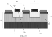
FIGS. 5A-5C show fabrication processes of manufacturing the device ofFIGS. 1A-1C . - The present disclosure relates to semiconductor structures and, more particularly, to devices with isolation structures in active regions and methods of manufacture. More specifically, the present disclosure relates to a high performance radio frequency (RF) device with embedded shallow trench isolation structures in an active region. For example, in embodiments, the shallow trench isolation structures (e.g., islands) may be embedded within an active region (RX) under an active gate structure and with a contact landing on the gate structure over the shallow trench isolation structures. The shallow trench isolation structures may be enclosed on all sides by the active region.
- Advantageously, the present disclosure provides a large width very short channel high performance RF device (high FT/Fmax), with a compact design (e.g., with a same footprint as a conventional Contact over Active Gate Process (COAG) RF multi-finger design). For example, the present disclosure maintains and/or improves FT of a wide device while improving Fmax. Moreover, advantageously, the device does not exhibit shorting between a raised source/drain (S/D) and the active gate structure. In addition, the processes for fabricating the devices are easily integrated with existing process flows with no additional masking steps.
- The devices of the present disclosure can be manufactured in a number of ways using a number of different tools. In general, though, the methodologies and tools are used to form structures with dimensions in the micrometer and nanometer scale. The methodologies, i.e., technologies, employed to manufacture the devices of the present disclosure have been adopted from integrated circuit (IC) technology. For example, the structures are built on wafers and are realized in films of material patterned by photolithographic processes on the top of a wafer. In particular, the fabrication of the devices uses three basic building blocks: (i) deposition of thin films of material on a substrate, (ii) applying a patterned mask on top of the films by photolithographic imaging, and (iii) etching the films selectively to the mask. In addition, precleaning processes may be used to clean etched surfaces of any contaminants, as is known in the art. Moreover, when necessary, rapid thermal anneal processes may be used to drive-in dopants or material layers as is known in the art.
-
FIG. 1A shows a top view of a device in accordance with aspects of the present disclosure.FIG. 1B shows a cross-sectional view of the device ofFIG. 1 along line A-A; whereasFIG. 1C shows a cross-sectional view of the device ofFIG. 1 along line B-B. In embodiments, thedevice 10 shown inFIGS. 1A-1C may be a multi-finger fully depleted semiconductor on insulator (FDSOI) MOSFET on a single diffusion region. - Referring to
FIGS. 1A-1C , thedevice 10 includes asemiconductor substrate 12. Thesemiconductor substrate 12 includes ahandle substrate 12a, a buriedinsulator layer 12b on thehandle substrate 12a and a top layer ofsemiconductor material 12c. Thehandle substrate 12a provides mechanical support to the buriedinsulator layer 12b and thetop semiconductor layer 12c. - In embodiments, the
handle substrate 12a andtop semiconductor material 12c may be composed of any suitable material including, but not limited to, Si, SiGe, SiGeC, SiC, alloys, GaAs, InAs, InP, and other III/V or II/VI compound semiconductors. In further embodiments, thehandle substrate 12a and thetop semiconductor layer 12c comprise a single crystalline semiconductor material, such as, for example, single crystalline silicon. Thehandle substrate 12a and thetop semiconductor layer 12c may also comprise any suitable crystallographic orientation (e.g., a (100), (110), (111), or (001) crystallographic orientation). The buriedinsulator layer 12b comprises any suitable material, including silicon oxide, sapphire, other suitable insulating materials, and/or combinations thereof. Anexemplary insulator layer 12b may be a buried oxide layer (BOX). - Shallow
trench isolation structures 14 may be formed in thesemiconductor substrate 12, e.g., extending to the buriedinsulator layer 12b. In embodiments, the shallowtrench isolation structures 14 may be separate islands embedded within the active region, e.g.,top semiconductor layer 12c. In embodiments, the shallowtrench isolation structures 14 can also be deep trench isolation structures. As further described herein, the shallow trench isolation structures 14 (e.g., islands of the shallow trench isolation structures 14) are undergate structures 16 and are enclosed on all sides with the active region, e.g.,top semiconductor material 12c. As in each of the embodiments, the shallowtrench isolation structures 14 may provide a stress enhancement on the channel of thegate structures 16. - Still referring to
FIGS. 1A-1C , thegate structures 16 may be formed over the shallowtrench isolation structures 14 and the active regions, e.g.,top semiconductor layer 12c. In embodiments, thegate structures 16 may overlap and be centered over the shallowtrench isolation structures 14. Thegate structures 16 can be implemented in a minimum gate length according to design rules. In embodiments, the shallowtrench isolation structures 14 will prevent shorting between raised diffusion regions (e.g., source and drain regions) 18 and thegate structures 16, e.g.,contacts 20b of thegate structures 16 andcontacts 20a of raised source and drainregions 18. Also, by having thegate structures 16 over the shallowtrench isolation structures 14 and the active regions, e.g.,top semiconductor layer 12c, device electrical characteristics show high FT/high Fmax at a wide active region. - The
gate structures 16 include agate dielectric material 16a, agate electrode 16b, andsidewall spacers 16c. In embodiments, thegate dielectric material 16a may be a high-k dielectric material or a low-k dielectric material. For example, the high-k dielectric material may be, e.g., HfO2 Al2O3, Ta2O3, TiO2, La2O3, SrTiO3, LaAlO3, ZrO2, Y2O3, Gd2O3, and combinations including multilayers thereof. Thegate electrode 16b may be a polysilicon material or a replacement metal gate material as is known in the art, e.g., Ti, TiAlC, Al, TiAl, TaN, TiN, TiC, Co, etc. Thesidewall spacers 16c may comprise nitride and/or oxide. - Although not critical to the understanding of the present disclosure, the
gate structures 16 can be fabricated using conventional CMOS processes. For example, thegate structures 16 can be fabricated using standard CMOS or replacement gate processes. In the standard CMOS processing, as further described herein, a gate dielectric and polysilicon are formed, e.g., deposited, on thetop semiconductor layer 12c, followed a patterning process. An insulator material such as nitride or oxide can be deposited on the patterned materials, followed by an anisotropic etching process to form thesidewall spacers 16c. -
FIGS. 1A-1C further show source/drain regions 18 formed on thetop semiconductor layer 12c between thegate structures 16. The source/drain regions 18 may be raised epitaxy regions formed by selectively growing a semiconductor material on thetop semiconductor layer 12c. -
Contacts gate electrode 16b and the source/drain regions 18.Wiring structures respective contacts wiring structures 24b may be aligned with the gate structures 16 (e.g., parallel with the gate structures 16); whereas thewiring structures 24a may be aligned with thecontacts 20a over the source/drain regions 18. Accordingly, in embodiments, thecontacts 20a may be formed to the source/drain regions 18 and thecontacts 20b may be formed to thegate electrode 16b, landing over the shallowtrench isolation structures 14. - The
contacts wiring structures dielectric material 22 to expose theunderlying gate electrode 16b and the source/drain regions 18, followed by a deposition process of a conductive material. In embodiments, for example, the conducive material may be Al or Tungsten, as examples. As further shown inFIG. 1A , for example, thecontacts 20b formed on thegate electrode 16b and thecontacts 20a formed on the source/drain regions 18 may be staggered, e.g., not aligned with one another. In addition, thecontacts 20b on thegate electrodes 16b are aligned over the shallowtrench isolation structures 16. - As should be understood by those of skill in the art, prior to the deposition process, a silicide process may be performed on the exposed
gate electrode 16b and the source/drain regions 18. The silicide process begins with deposition of a thin transition metal layer, e.g., nickel, cobalt or titanium, over fully formed raised source/drain regions 18 andgate electrode 16b. After deposition of the material, the structure is heated allowing the transition metal to react with exposed silicon (or other semiconductor material as described herein) in the active regions of the semiconductor device (e.g., raised source/drain regions 18 andgate electrode 16b) forming a low-resistance transition metal silicide. Following the reaction, any remaining transition metal is removed by chemical etching, leaving silicide contacts in the active regions of the device. It should be understood by those of skill in the art that silicide contacts will not be required on the devices, when a gate structure is composed of a metal material. -
FIG. 2 shows a top view of a device in accordance with additional aspects of the present disclosure. In thedevice 10a ofFIG. 2 , multipleactive regions 12x are shown, each separated by arespective isolation structure 26. Theisolation structure 26 may be a shallow trench isolation structure or a deep trench isolation structure. The multipleactive regions 12x may be separated by a minimum distance allowed by design rules. Thegate structures 16 extend over the multipleactive regions 12x, and each of theactive regions 12x include the shallowtrench isolation structures 14 embedded within theactive region 12x and aligned with (overlapping) thegate structures 16. The remaining features of thedevice 10a ofFIG. 2 are similar to thedevice 10 described with respect toFIGS. 1A-1C . -
FIG. 3 shows a top view of a device in accordance with further aspects of the present disclosure. In thedevice 10b ofFIG. 3 , thecontacts 20b for thegate structures 16 are provided above and below theactive region 12a. That is, thecontacts 20b may be placed beyond theactive region 12a on opposite edges ofgate structures 16 before termination of thegate structures 16. In this way, thecontacts 20b for thegate structures 16 are perpendicular to thegate structures 16 and are not provided on or aligned with the shallowtrench isolation structures 14. In embodiments, thewiring structures 24b extend over themultiple contacts 20b for thegate structures 16, e.g., parallel and aligned with thecontacts 20b for thegate structures 16. In alternative embodiments, the shallowtrench isolation structures 14 may be deep trench isolation structures extending through the buriedinsulator layer 12b. The remaining features of thedevice 10b ofFIG. 3 are similar to thedevice 10 described with respect toFIGS. 1A-1C . -
FIG. 4 shows a top view of a device in accordance with additional aspects of the present disclosure. In thedevice 10c ofFIG. 4 , multipleactive regions 12x are shown, each separated by theisolation structure 26. The multipleactive regions 12x may be separated by a minimum distance allowed by design rules as already described herein. Thegate structures 16 extend over the multipleactive regions 12x, and each of theactive regions 12x includes the shallowtrench isolation structures 14 embedded within theactive region 12x and aligned with thegate structures 16. Thecontacts 20b for thegate structures 16 are provided above and below each of theactive regions 12x. That is, similar to that shown inFIG. 3 , thecontacts 20b may be placed beyond theactive regions 12x. In this way, thecontacts 20b for thegate structures 16 are perpendicular to thegate structures 16 and are not provided on or aligned with the shallowtrench isolation structures 14. In embodiments, thewiring structures 24b extend over themultiple contacts 20b for thegate structures 16, e.g., parallel and aligned with thecontacts 20b for thegate structures 16. The remaining features of thedevice 10c ofFIG. 4 are similar to thedevice 10b described with respect toFIG. 3 . -
FIGS. 5A-5C show fabrication processes of manufacturing thedevice 10 ofFIGS. 1A-1C . InFIG. 5A , shallowtrench isolation structures 14 are formed in thesubstrate 12. The shallowtrench isolation structures 14 can be formed by conventional lithography, etching and deposition methods known to those of skill in the art. For example, a resist formed over thetop semiconductor layer 12c is exposed to energy (light) and developed utilizing a conventional resist developer to form a pattern (opening). An etching process with a selective chemistry, e.g., reactive ion etching (RIE), will be used to transfer the pattern from the photoresist layer to thetop semiconductor layer 12c to form one or more trenches in thetop semiconductor layer 12c and extending into the buriedinsulator layer 12b through the openings of the resist. Following the resist removal by a conventional oxygen ashing process or other known stripants, the insulator material (e.g., SiO2) can be deposited by any conventional deposition processes, e.g., chemical vapor deposition (CVD) processes. Any residual material on the surface of thetop semiconductor layer 12c can be removed by conventional chemical mechanical polishing (CMP) processes. This process can also be used to form deep trench isolation structures. - In
FIG. 5B , thegate structures 16 are formed over the shallowtrench isolation structures 14. In embodiments, thegate structures 16 can be formed by depositing thegate dielectric material 16a over the shallowtrench isolation structures 16 and the active regions, e.g.,top semiconductor layer 12c. Thegate dielectric material 16a may be blanket deposited using CVD, Plasma Enhanced CVD (PECVD) or atomic layer deposition (ALD), as examples. Thegate electrode 16b, e.g., polysilicon, may be blanket deposited over thegate dielectric material 16a using a conventional CVD process. Thegate dielectric material 16a and thegate electrode 16b may be patterned using conventional lithography and etching processes as described herein. Thesidewall spacers 16c may be formed by a deposition (e.g., CVD) of nitride and/or oxide, followed by an anisotropic etching process. - In
FIG. 5C , the source/drain regions 18 may be formed on the active regions, e.g.,top semiconductor layer 12c. In accordance with exemplary embodiments, the source/drain regions 18 may be raised epitaxy regions comprising SiGe or Si as examples. In accordance with alternative embodiments of the present disclosure, the epitaxy regions may be formed of a III-V compound semiconductor such as GaAs, InP, GaN, InGaAs, InAlAs, GaSb, AlSb, AlAs, AlP, GaP, combinations thereof, or multilayers thereof. Depending on whether the resulting device is a p-type FET or an n-type FET, a p-type or an n-type impurity may be in-situ doped. For example, when the resulting FET is a p-type FET, silicon germanium boron (SiGeB) may be grown. Conversely, when the resulting FET is an n-type FET, silicon phosphorous (SiP) or silicon carbon phosphorous (SiCP) may be grown. -
FIGS. 1A-1C show the fabrication of thecontacts wiring structures - The devices can be utilized in system on chip (SoC) technology. The SoC is an integrated circuit (also known as a "chip") that integrates all components of an electronic system on a single chip or substrate. As the components are integrated on a single substrate, SoCs consume much less power and take up much less area than multichip designs with equivalent functionality. Because of this, SoCs are becoming the dominant force in the mobile computing (such as in Smartphones) and edge computing markets. SoC is also used in embedded systems and the Internet of Things.
- The method(s) as described above is used in the fabrication of integrated circuit chips. The resulting integrated circuit chips can be distributed by the fabricator in raw wafer form (that is, as a single wafer that has multiple unpackaged chips), as a bare die, or in a packaged form. In the latter case the chip is mounted in a single chip package (such as a plastic carrier, with leads that are affixed to a motherboard or other higher level carrier) or in a multichip package (such as a ceramic carrier that has either or both surface interconnections or buried interconnections). In any case the chip is then integrated with other chips, discrete circuit elements, and/or other signal processing devices as part of either (a) an intermediate product, such as a motherboard, or (b) an end product. The end product can be any product that includes integrated circuit chips, ranging from toys and other low-end applications to advanced computer products having a display, a keyboard or other input device, and a central processor.
- The descriptions of the various embodiments of the present disclosure have been presented for purposes of illustration, but are not intended to be exhaustive or limited to the embodiments disclosed. Many modifications and variations will be apparent to those of ordinary skill in the art without departing from the scope and spirit of the described embodiments. The terminology used herein was chosen to best explain the principles of the embodiments, the practical application or technical improvement over technologies found in the marketplace, or to enable others of ordinary skill in the art to understand the embodiments disclosed herein.
Claims (15)
- A structure comprising:an active region;a plurality of isolation structures within the active region;a plurality of gate structures overlapping the plurality of isolation structures within the active region; anddiffusion regions on sides of the plurality of gate structures and the plurality of isolation structures.
- The structure of claim 1, wherein the plurality of isolation structures comprise shallow trench isolation structures embedded within the active region, or wherein the plurality of isolation structures are deep trench isolation structures.
- The structure of claim 1 or claim 2, wherein the plurality of isolation structures are surrounded by a top semiconductor layer comprising the active region.
- The structure of one of claims 1 to 3, wherein the plurality of gate structures comprises polysilicon gate structures which overlap with the plurality of isolation structures and the active region.
- The structure of one of claims 1 to 4, further comprising contacts to the gate structures and contacts to the diffusion regions over the active region.
- The structure of claim 5, wherein the contacts to the gate structures are over the plurality of isolation structures, or wherein the contacts to the gate structures extend at opposing ends of the gate structures.
- The structure of claim 6, wherein the contacts to the gate structures are offset from the contacts to the diffusion regions.
- The structure of claim 5, wherein the active region comprises plural active regions, the gate structures extend over the plural active regions and the contacts to the gate structures are provided between the plural active regions.
- A structure comprising:at least one active region;a plurality of isolation structures within the at least one active region;a plurality of gate structures overlapping the plurality of isolation structures within the at least one active region;raised source/drain regions on sides of the plurality of gate structures and the plurality of isolation structures;a first set of contacts to the raised source/drain regions; anda second set of contacts to the plurality of gate structures.
- The structure of claim 9, wherein the plurality of isolation structures comprise islands embedded within the at least one active region.
- The structure of claim 9 or claim 10, wherein the second set of contacts overlap with the plurality of isolation structures, or wherein the second set of contacts are at opposing ends of the plurality of gate structures.
- The structure of claim 11, wherein the second set of contacts are offset from the first set of contacts.
- The structure of claim 10, wherein the at least one active region comprises a plurality of active regions and the second set of contacts are provided at ends of each of plurality of the active regions, and, optionally, wherein the plurality of gate structures extend between the plurality of active regions and over isolation regions that isolate each of the active regions from one another.
- The structure of one of claims 9 to 13, further comprising wiring structures contacting the second set of contacts and which are parallel to the plurality of gate structures, or which are perpendicular to the plurality of gate structures.
- A method comprising:forming a plurality of isolation structures within an active region;forming a plurality of gate structures overlapping the plurality of isolation structures within the active region;forming diffusion regions on sides of the plurality of gate structures and the plurality of isolation structures; andforming contacts to the diffusion regions and the plurality of gate structures.
Applications Claiming Priority (1)
| Application Number | Priority Date | Filing Date | Title |
|---|---|---|---|
| US18/095,746 US12610615B2 (en) | 2023-01-11 | 2023-01-11 | Device with isolation structures in active regions |
Publications (1)
| Publication Number | Publication Date |
|---|---|
| EP4401123A1 true EP4401123A1 (en) | 2024-07-17 |
Family
ID=88923670
Family Applications (1)
| Application Number | Title | Priority Date | Filing Date |
|---|---|---|---|
| EP23211353.0A Pending EP4401123A1 (en) | 2023-01-11 | 2023-11-22 | Device with isolation structures in active regions |
Country Status (5)
| Country | Link |
|---|---|
| US (1) | US12610615B2 (en) |
| EP (1) | EP4401123A1 (en) |
| KR (1) | KR102863229B1 (en) |
| CN (1) | CN118335738A (en) |
| TW (1) | TW202431635A (en) |
Cited By (1)
| Publication number | Priority date | Publication date | Assignee | Title |
|---|---|---|---|---|
| US20240234425A1 (en) * | 2023-01-11 | 2024-07-11 | Globalfoundries U.S. Inc. | Device with isolation structures in active regions |
Families Citing this family (1)
| Publication number | Priority date | Publication date | Assignee | Title |
|---|---|---|---|---|
| TWI903736B (en) * | 2024-09-04 | 2025-11-01 | 雋佾科技股份有限公司 | Semiconductor device and manufacturing method thereof |
Citations (5)
| Publication number | Priority date | Publication date | Assignee | Title |
|---|---|---|---|---|
| US7078775B2 (en) * | 2003-04-18 | 2006-07-18 | Samsung Electronics Co., Ltd. | MOS transistor having a mesh-type gate electrode |
| US20070158762A1 (en) * | 2006-01-11 | 2007-07-12 | Anderson Brent A | Low-capacitance contact for long gate-length devices with small contacted pitch |
| US20080179635A1 (en) * | 2007-01-30 | 2008-07-31 | Infineon Technologies | Fin interconnects for multigate fet circuit blocks |
| US20110221009A1 (en) * | 2010-03-10 | 2011-09-15 | Taiwan Semiconductor Manufacturing Company, Ltd. | Method and apparatus for reducing gate resistance |
| US8952424B2 (en) * | 2008-12-22 | 2015-02-10 | Cambridge Silicon Radio Ltd | RF CMOS transistor design |
Family Cites Families (27)
| Publication number | Priority date | Publication date | Assignee | Title |
|---|---|---|---|---|
| US7074623B2 (en) * | 2002-06-07 | 2006-07-11 | Amberwave Systems Corporation | Methods of forming strained-semiconductor-on-insulator finFET device structures |
| US8404560B2 (en) * | 2010-10-12 | 2013-03-26 | International Business Machines Corporation | Devices with gate-to-gate isolation structures and methods of manufacture |
| US9461143B2 (en) | 2012-09-19 | 2016-10-04 | Intel Corporation | Gate contact structure over active gate and method to fabricate same |
| US9245903B2 (en) * | 2014-04-11 | 2016-01-26 | International Business Machines Corporation | High voltage metal oxide semiconductor field effect transistor integrated into extremely thin semiconductor on insulator process |
| KR102235614B1 (en) * | 2014-09-17 | 2021-04-02 | 삼성전자주식회사 | Integrated circuit device and method of manufacturing the same |
| KR102177431B1 (en) * | 2014-12-23 | 2020-11-11 | 주식회사 키 파운드리 | Semiconductor device |
| FR3037714A1 (en) * | 2015-06-18 | 2016-12-23 | St Microelectronics Crolles 2 Sas | METHOD FOR MAKING A CONTACT ON AN ACTIVE ZONE OF AN INTEGRATED CIRCUIT, FOR EXAMPLE ON A SOI SUBSTRATE, IN PARTICULAR FDSOI, AND INTEGRATED CIRCUIT CORRESPONDING |
| US9704971B2 (en) * | 2015-12-09 | 2017-07-11 | Globalfoundries Inc. | Epi facet height uniformity improvement for FDSOI technologies |
| US9917103B1 (en) * | 2017-01-04 | 2018-03-13 | Globalfoundries Inc. | Diffusion break forming after source/drain forming and related IC structure |
| US10164006B1 (en) | 2017-10-30 | 2018-12-25 | Globalfoundries Inc. | LDMOS FinFET structures with trench isolation in the drain extension |
| US11411095B2 (en) * | 2017-11-30 | 2022-08-09 | Intel Corporation | Epitaxial source or drain structures for advanced integrated circuit structure fabrication |
| US10529860B2 (en) * | 2018-05-31 | 2020-01-07 | Taiwan Semiconductor Manufacturing Co., Ltd. | Structure and method for FinFET device with contact over dielectric gate |
| US11121129B2 (en) * | 2018-07-31 | 2021-09-14 | Taiwan Semiconductor Manufacturing Company, Ltd. | Semiconductor device |
| US10957578B2 (en) * | 2018-09-28 | 2021-03-23 | Globalfoundries U.S. Inc. | Single diffusion break device for FDSOI |
| US10756184B2 (en) * | 2018-11-05 | 2020-08-25 | Globalfoundries Inc. | Faceted epitaxial source/drain regions |
| US11031484B2 (en) * | 2019-06-28 | 2021-06-08 | Globalfoundries U.S. Inc. | Silicided gate structures |
| CN110416104B (en) * | 2019-07-25 | 2021-03-26 | 华东师范大学 | Method for extracting gate-surrounding parasitic interconnection capacitance of source-drain lifted FDSOI device |
| US11127831B2 (en) * | 2019-09-24 | 2021-09-21 | Globalfoundries U.S. Inc. | Transistor structure with overlying gate on polysilicon gate structure and related method |
| US11791389B2 (en) | 2021-01-08 | 2023-10-17 | Wolfspeed, Inc. | Radio frequency transistor amplifiers having widened and/or asymmetric source/drain regions for improved on-resistance performance |
| US12419084B2 (en) | 2021-05-13 | 2025-09-16 | Taiwan Semiconductor Manufacturing Co., Ltd. | Methods of forming transistor source/drain regions comprising carbon liner layers |
| US11855179B2 (en) | 2021-06-03 | 2023-12-26 | Taiwan Semiconductor Manufacturing Company Limited | Semiconductor devices and methods of manufacturing thereof |
| US11798948B2 (en) * | 2021-10-07 | 2023-10-24 | Globalfoundries U.S. Inc. | Semiconductor structure with shared well |
| US20230146952A1 (en) * | 2021-11-08 | 2023-05-11 | Globalfoundries U.S. Inc. | Transistor with faceted, raised source/drain region |
| US12020937B2 (en) * | 2022-03-23 | 2024-06-25 | Globalfoundries U.S. Inc. | Carbon implantation for thicker gate silicide |
| US12610615B2 (en) * | 2023-01-11 | 2026-04-21 | Globalfoundries U.S. Inc | Device with isolation structures in active regions |
| US20240339527A1 (en) * | 2023-04-06 | 2024-10-10 | Globalfoundries U.S. Inc. | Low capacitance and low resistance devices |
| US20250089317A1 (en) * | 2023-09-08 | 2025-03-13 | Globalfoundries U.S. Inc. | Nanosheet structures with bottom semiconductor material |
-
2023
- 2023-01-11 US US18/095,746 patent/US12610615B2/en active Active
- 2023-11-22 EP EP23211353.0A patent/EP4401123A1/en active Pending
- 2023-12-08 CN CN202311689006.XA patent/CN118335738A/en active Pending
- 2023-12-11 TW TW112148153A patent/TW202431635A/en unknown
- 2023-12-12 KR KR1020230179309A patent/KR102863229B1/en active Active
Patent Citations (5)
| Publication number | Priority date | Publication date | Assignee | Title |
|---|---|---|---|---|
| US7078775B2 (en) * | 2003-04-18 | 2006-07-18 | Samsung Electronics Co., Ltd. | MOS transistor having a mesh-type gate electrode |
| US20070158762A1 (en) * | 2006-01-11 | 2007-07-12 | Anderson Brent A | Low-capacitance contact for long gate-length devices with small contacted pitch |
| US20080179635A1 (en) * | 2007-01-30 | 2008-07-31 | Infineon Technologies | Fin interconnects for multigate fet circuit blocks |
| US8952424B2 (en) * | 2008-12-22 | 2015-02-10 | Cambridge Silicon Radio Ltd | RF CMOS transistor design |
| US20110221009A1 (en) * | 2010-03-10 | 2011-09-15 | Taiwan Semiconductor Manufacturing Company, Ltd. | Method and apparatus for reducing gate resistance |
Non-Patent Citations (1)
| Title |
|---|
| WATTS JOSEF ET AL: "RF-pFET in fully depleted SOI demonstrates 420 GHz FT", 2017 IEEE RADIO FREQUENCY INTEGRATED CIRCUITS SYMPOSIUM (RFIC), IEEE, 4 June 2017 (2017-06-04), pages 84 - 87, XP033115753, DOI: 10.1109/RFIC.2017.7969023 * |
Cited By (2)
| Publication number | Priority date | Publication date | Assignee | Title |
|---|---|---|---|---|
| US20240234425A1 (en) * | 2023-01-11 | 2024-07-11 | Globalfoundries U.S. Inc. | Device with isolation structures in active regions |
| US12610615B2 (en) * | 2023-01-11 | 2026-04-21 | Globalfoundries U.S. Inc | Device with isolation structures in active regions |
Also Published As
| Publication number | Publication date |
|---|---|
| KR20240112195A (en) | 2024-07-18 |
| US20240234425A1 (en) | 2024-07-11 |
| TW202431635A (en) | 2024-08-01 |
| KR102863229B1 (en) | 2025-09-24 |
| CN118335738A (en) | 2024-07-12 |
| US12610615B2 (en) | 2026-04-21 |
Similar Documents
| Publication | Publication Date | Title |
|---|---|---|
| US10777468B1 (en) | Stacked vertical field-effect transistors with sacrificial layer patterning | |
| US9761491B1 (en) | Self-aligned deep contact for vertical FET | |
| EP4369408A1 (en) | Transistor with metal field plate contact | |
| KR102863229B1 (en) | Device with isolation structures in active regions | |
| US12289913B1 (en) | Device with metal field plate extension | |
| US12408373B1 (en) | Device with three dimensional channel | |
| US12336243B2 (en) | Lateral bipolar transistor with gated collector | |
| US12159926B2 (en) | Lateral bipolar transistor | |
| US20250089317A1 (en) | Nanosheet structures with bottom semiconductor material | |
| KR20230004951A (en) | Horizontal gaa nano-wire and nano-slab transistors | |
| US12446290B2 (en) | Asymmetric gate extension in stacked FET | |
| CN119947165A (en) | High electron mobility transistor with regenerative barrier | |
| US11705508B2 (en) | Single fin structures | |
| US10446654B1 (en) | Gate contact structures and self-aligned contact process | |
| US20250234585A1 (en) | Extended drain metal oxide semiconductor (edmos) field effect transistor (fet) with dual thickness semiconductor material | |
| US12324217B2 (en) | Laterally diffused metal-oxide semiconductor with gate contact | |
| US20260123005A1 (en) | Transistor with field plate | |
| EP4531112A1 (en) | Spin qubit devices comprising qubit gates and self-aligned barrier gates | |
| US12495575B2 (en) | Multi-channel replacement metal gate device | |
| US20250031401A1 (en) | Nanosheet structures with corner spacer | |
| US11935927B2 (en) | Bipolar transistor with collector contact | |
| US11804542B2 (en) | Annular bipolar transistors | |
| EP4383345A1 (en) | High-electron-mobility transistor (hemt) | |
| US20260068279A1 (en) | Extended drain metal oxide semiconductor device | |
| EP4535429A1 (en) | High-electron-mobility transistor |
Legal Events
| Date | Code | Title | Description |
|---|---|---|---|
| PUAI | Public reference made under article 153(3) epc to a published international application that has entered the european phase |
Free format text: ORIGINAL CODE: 0009012 |
|
| STAA | Information on the status of an ep patent application or granted ep patent |
Free format text: STATUS: THE APPLICATION HAS BEEN PUBLISHED |
|
| AK | Designated contracting states |
Kind code of ref document: A1 Designated state(s): AL AT BE BG CH CY CZ DE DK EE ES FI FR GB GR HR HU IE IS IT LI LT LU LV MC ME MK MT NL NO PL PT RO RS SE SI SK SM TR |
|
| STAA | Information on the status of an ep patent application or granted ep patent |
Free format text: STATUS: REQUEST FOR EXAMINATION WAS MADE |
|
| 17P | Request for examination filed |
Effective date: 20241125 |
|
| RBV | Designated contracting states (corrected) |
Designated state(s): AL AT BE BG CH CY CZ DE DK EE ES FI FR GB GR HR HU IE IS IT LI LT LU LV MC ME MK MT NL NO PL PT RO RS SE SI SK SM TR |