EP4400883A2 - Directional couplers with heterogenous claddings - Google Patents
Directional couplers with heterogenous claddings Download PDFInfo
- Publication number
- EP4400883A2 EP4400883A2 EP23205378.5A EP23205378A EP4400883A2 EP 4400883 A2 EP4400883 A2 EP 4400883A2 EP 23205378 A EP23205378 A EP 23205378A EP 4400883 A2 EP4400883 A2 EP 4400883A2
- Authority
- EP
- European Patent Office
- Prior art keywords
- segments
- sidewall
- cladding layer
- refractive index
- waveguide core
- Prior art date
- Legal status (The legal status is an assumption and is not a legal conclusion. Google has not performed a legal analysis and makes no representation as to the accuracy of the status listed.)
- Granted
Links
Images


Classifications
-
- G—PHYSICS
- G02—OPTICS
- G02B—OPTICAL ELEMENTS, SYSTEMS OR APPARATUS
- G02B6/00—Light guides; Structural details of arrangements comprising light guides and other optical elements, e.g. couplings
- G02B6/10—Light guides; Structural details of arrangements comprising light guides and other optical elements, e.g. couplings of the optical waveguide type
- G02B6/12—Light guides; Structural details of arrangements comprising light guides and other optical elements, e.g. couplings of the optical waveguide type of the integrated circuit kind
- G02B6/12004—Combinations of two or more optical elements
-
- G—PHYSICS
- G02—OPTICS
- G02B—OPTICAL ELEMENTS, SYSTEMS OR APPARATUS
- G02B6/00—Light guides; Structural details of arrangements comprising light guides and other optical elements, e.g. couplings
- G02B6/10—Light guides; Structural details of arrangements comprising light guides and other optical elements, e.g. couplings of the optical waveguide type
- G02B6/12—Light guides; Structural details of arrangements comprising light guides and other optical elements, e.g. couplings of the optical waveguide type of the integrated circuit kind
- G02B6/122—Basic optical elements, e.g. light-guiding paths
- G02B6/124—Geodesic lenses or integrated gratings
-
- G—PHYSICS
- G02—OPTICS
- G02B—OPTICAL ELEMENTS, SYSTEMS OR APPARATUS
- G02B6/00—Light guides; Structural details of arrangements comprising light guides and other optical elements, e.g. couplings
- G02B6/10—Light guides; Structural details of arrangements comprising light guides and other optical elements, e.g. couplings of the optical waveguide type
- G02B6/12—Light guides; Structural details of arrangements comprising light guides and other optical elements, e.g. couplings of the optical waveguide type of the integrated circuit kind
- G02B6/122—Basic optical elements, e.g. light-guiding paths
- G02B6/125—Bends, branchings or intersections
-
- G—PHYSICS
- G02—OPTICS
- G02B—OPTICAL ELEMENTS, SYSTEMS OR APPARATUS
- G02B6/00—Light guides; Structural details of arrangements comprising light guides and other optical elements, e.g. couplings
- G02B6/10—Light guides; Structural details of arrangements comprising light guides and other optical elements, e.g. couplings of the optical waveguide type
- G02B6/12—Light guides; Structural details of arrangements comprising light guides and other optical elements, e.g. couplings of the optical waveguide type of the integrated circuit kind
- G02B6/13—Integrated optical circuits characterised by the manufacturing method
-
- G—PHYSICS
- G02—OPTICS
- G02B—OPTICAL ELEMENTS, SYSTEMS OR APPARATUS
- G02B6/00—Light guides; Structural details of arrangements comprising light guides and other optical elements, e.g. couplings
- G02B6/24—Coupling light guides
- G02B6/26—Optical coupling means
- G02B6/28—Optical coupling means having data bus means, i.e. plural waveguides interconnected and providing an inherently bidirectional system by mixing and splitting signals
- G02B6/2804—Optical coupling means having data bus means, i.e. plural waveguides interconnected and providing an inherently bidirectional system by mixing and splitting signals forming multipart couplers without wavelength selective elements, e.g. "T" couplers, star couplers
- G02B6/2821—Optical coupling means having data bus means, i.e. plural waveguides interconnected and providing an inherently bidirectional system by mixing and splitting signals forming multipart couplers without wavelength selective elements, e.g. "T" couplers, star couplers using lateral coupling between contiguous fibres to split or combine optical signals
-
- G—PHYSICS
- G02—OPTICS
- G02B—OPTICAL ELEMENTS, SYSTEMS OR APPARATUS
- G02B6/00—Light guides; Structural details of arrangements comprising light guides and other optical elements, e.g. couplings
- G02B6/24—Coupling light guides
- G02B6/26—Optical coupling means
- G02B6/34—Optical coupling means utilising prism or grating
-
- G—PHYSICS
- G02—OPTICS
- G02F—OPTICAL DEVICES OR ARRANGEMENTS FOR THE CONTROL OF LIGHT BY MODIFICATION OF THE OPTICAL PROPERTIES OF THE MEDIA OF THE ELEMENTS INVOLVED THEREIN; NON-LINEAR OPTICS; FREQUENCY-CHANGING OF LIGHT; OPTICAL LOGIC ELEMENTS; OPTICAL ANALOGUE/DIGITAL CONVERTERS
- G02F1/00—Devices or arrangements for the control of the intensity, colour, phase, polarisation or direction of light arriving from an independent light source, e.g. switching, gating or modulating; Non-linear optics
- G02F1/29—Devices or arrangements for the control of the intensity, colour, phase, polarisation or direction of light arriving from an independent light source, e.g. switching, gating or modulating; Non-linear optics for the control of the position or the direction of light beams, i.e. deflection
- G02F1/31—Digital deflection, i.e. optical switching
- G02F1/313—Digital deflection, i.e. optical switching in an optical waveguide structure
- G02F1/3132—Digital deflection, i.e. optical switching in an optical waveguide structure of directional coupler type
-
- G—PHYSICS
- G02—OPTICS
- G02B—OPTICAL ELEMENTS, SYSTEMS OR APPARATUS
- G02B6/00—Light guides; Structural details of arrangements comprising light guides and other optical elements, e.g. couplings
- G02B6/10—Light guides; Structural details of arrangements comprising light guides and other optical elements, e.g. couplings of the optical waveguide type
- G02B6/12—Light guides; Structural details of arrangements comprising light guides and other optical elements, e.g. couplings of the optical waveguide type of the integrated circuit kind
- G02B2006/12133—Functions
- G02B2006/12147—Coupler
-
- G—PHYSICS
- G02—OPTICS
- G02B—OPTICAL ELEMENTS, SYSTEMS OR APPARATUS
- G02B6/00—Light guides; Structural details of arrangements comprising light guides and other optical elements, e.g. couplings
- G02B6/24—Coupling light guides
- G02B6/26—Optical coupling means
- G02B6/28—Optical coupling means having data bus means, i.e. plural waveguides interconnected and providing an inherently bidirectional system by mixing and splitting signals
- G02B6/293—Optical coupling means having data bus means, i.e. plural waveguides interconnected and providing an inherently bidirectional system by mixing and splitting signals with wavelength selective means
- G02B6/29331—Optical coupling means having data bus means, i.e. plural waveguides interconnected and providing an inherently bidirectional system by mixing and splitting signals with wavelength selective means operating by evanescent wave coupling
- G02B6/29335—Evanescent coupling to a resonator cavity, i.e. between a waveguide mode and a resonant mode of the cavity
- G02B6/29338—Loop resonators
Definitions
- the disclosure relates to photonics chips and, more specifically, to structures for a directional coupler and methods of forming a structure for a directional coupler.
- Photonics chips are used in many applications and systems including, but not limited to, data communication systems and data computation systems.
- a photonics chip may integrate optical components and electronic components into a unified platform. Among other factors, layout area, cost, and operational overhead may be reduced by the integration of both types of components on the same chip.
- a directional coupler is employed on a photonics chip to split propagating optical signals between different waveguide cores.
- a directional coupler includes sections of the different waveguide cores that are separated by a gap that is selected to promote optical coupling over a given coupling length.
- the dimension of the gap between the sections of the waveguide cores may be reduced to enhance the coupling strength and reduce the device footprint.
- reducing the dimension of the gap may increase the difficulty in patterning the gap between the waveguide cores and the difficulty in subsequently filling the gap with dielectric material. For example, air voids may be created within the dielectric material during deposition.
- a structure for a directional coupler comprises a first waveguide core including a first plurality of segments arranged along a first longitudinal axis, and a second waveguide core including a second plurality of segments arranged along a second longitudinal axis.
- Each of the first plurality of segments has a first sidewall and a second sidewall opposite to the first sidewall
- each of the second plurality of segments has a first sidewall and a second sidewall opposite to the first sidewall
- the first sidewall of each of the second plurality of segments is disposed adjacent to the first sidewall of one of the first plurality of segments in a coupling region.
- the structure further comprises a first cladding layer comprising a first material that has a first refractive index, and a second cladding layer comprising a second material that has a second refractive index different from the first refractive index.
- the first cladding layer adjoins the first sidewall of each of the first plurality of segments and the first sidewall of each of the second plurality of segments
- the second cladding layer adjoins the second sidewall of each of the first plurality of segments and the second sidewall of each of the second plurality of segments.
- the second refractive index of the second material may be greater than the first refractive index of the first material.
- the second refractive index of the second material may be less than the first refractive index of the first material.
- the first material may comprise a first non-ferroelectric material
- the second material may comprise a second non-ferroelectric material.
- the first material may comprise a silicon nitride
- the second material may comprise silicon dioxid.
- the first waveguide core may include a first plurality of gaps that alternate with the first plurality of segments along the first longitudinal axis.
- the second waveguide core may include a second plurality of gaps that alternate with the second plurality of segments along the second longitudinal axis.
- the first cladding layer may be disposed in the first plurality of gaps and the second plurality of gaps.
- the first waveguide core may include a first plurality of gaps that alternate with the first plurality of segments along the first longitudinal axis.
- the second waveguide core may include a second plurality of gaps that alternate with the first plurality of segments along the second longitudinal axis.
- the second cladding layer may be disposed in the first plurality of gaps and the second plurality of gaps.
- each of the first plurality of segments may have a bottom surface
- each of the second plurality of segments may have a bottom surface
- the structure may further comprise a dielectric layer comprised of a dielectric material, wherein the bottom surface of each of the first plurality of segments may be disposed on the dielectric layer, and the bottom surface of each of the second plurality of segments may be disposed on the dielectric layer.
- the dielectric material may have a third refractive index that is different from the first refractive index; additionally or alternatively, the first cladding layer and the second cladding layer may be disposed on the dielectric layer.
- each of the first plurality of segments may further have a top surface
- each of the second plurality of segments may have a top surface
- the structure may further comprise a dielectric layer comprised of a dielectric material, wherein the dielectric layer may be disposed on the top surface of each of the first plurality of segments, and the dielectric layer may be disposed on the top surface of each of the second plurality of segments.
- the dielectric material may have a third refractive index that is different from the first refractive index; additionally or alternatively, the dielectric layer may be disposed on the first cladding layer and the second cladding layer.
- a structure for a directional coupler comprises a first waveguide core having a first sidewall and a second sidewall opposite to the first sidewall, and a second waveguide core having a first sidewall and a second sidewall opposite to the first sidewall.
- the first sidewall of the second waveguide core spaced from the first sidewall of the first waveguide core by a gap in a coupling region.
- the structure further comprises a first cladding layer comprising a first material that has a first refractive index, and a second cladding layer comprising a second material that has a second refractive index different from the first refractive index.
- the first cladding layer includes a first plurality of sections in the gap
- the second cladding layer includes a second plurality of sections in the gap
- the second plurality of sections of the second cladding layer alternate with the first plurality of sections of the first cladding layer.
- the second cladding layer of the structure may be disposed adjacent to the second sidewall of the first waveguide core, and the second cladding layer may be disposed adjacent to the second sidewall of the second waveguide core.
- the second refractive index may be greater than the first refractive index; alternatively, the second refractive index may be less than the first refractive index.
- first plurality of sections of the first cladding layer and the second plurality of sections of the second cladding layer may define a sub-wavelength grating.
- the first material may comprise a first non-ferroelectric material
- the second material comprises a second non-ferroelectric material
- a method of forming a structure for a directional coupler comprises forming a first waveguide core including a first plurality of segments arranged along a first longitudinal axis, and forming a second waveguide core including a second plurality of segments arranged along a second longitudinal axis.
- Each of the first plurality of segments has a first sidewall and a second sidewall opposite to the first sidewall
- each of the second plurality of segments has a first sidewall and a second sidewall opposite to the first sidewall
- the first sidewall of each of the second plurality of segments is disposed adjacent to the first sidewall of one of the first plurality of segments in a coupling region.
- the method further comprises forming a first cladding layer comprised of a first material having a first refractive index, and forming a second cladding layer comprised of a second material that has a second refractive index different from the first refractive index.
- the first cladding layer adjoins the first sidewall of each of the first plurality of segments and the first sidewall of each of the second plurality of segments
- the second cladding layer adjoins the second sidewall of each of the first plurality of segments and the second sidewall of each of the second plurality of segments.
- a structure 10 for a directional coupler includes a waveguide core 12 and a waveguide core 14 that are positioned on, and over, a dielectric layer 16 and a semiconductor substrate 18.
- the dielectric layer 16 may be comprised of a dielectric material, such as silicon dioxide, and the semiconductor substrate 18 may be comprised of a semiconductor material, such as single-crystal silicon.
- the dielectric layer 16 may be a buried oxide layer of a silicon-on-insulator substrate, and the dielectric layer 16 may be disposed between the waveguide cores 12, 14 and the semiconductor substrate 18.
- the dielectric layer 16 may function as an underlying cladding layer for the waveguide cores 12, 14.
- the waveguide core 12 includes multiple segments 30 that are distributed in an input region 20, a coupling region 22, and an output region 24.
- the segments 30 are positioned in a spaced-apart arrangement in which spaces or gaps G1 alternate with the segments 30.
- the segments 30 In the coupling region 22, the segments 30 alternate with the gaps G1 along the longitudinal axis 32.
- the segments 30 may be arranged with curved routing that approximates respective bends.
- the pitch and duty cycle of the segments 30 may be uniform to define a periodic arrangement.
- the pitch and/or the duty cycle of the segments 30 may be apodized (i.e., non-uniform) to define a non-periodic arrangement.
- a rib may be overlaid with some or all of the segments 30.
- the waveguide core 14 includes multiple segments 34 that are distributed in the input region 20, the coupling region 22, and the output region 24.
- the segments 34 are positioned in a spaced-apart arrangement in which spaces or gaps G2 alternate with the segments 34.
- the segments 34 and the gaps G2 alternate along the longitudinal axis 36.
- the segments 34 may be arranged with curved routing that approximates respective bends.
- the pitch and duty cycle of the segments 34 may be uniform to define a periodic arrangement.
- the pitch and/or the duty cycle of the segments 34 may be apodized (i.e., non-uniform) to define a non-periodic arrangement.
- a rib may be overlaid with some or all of the segments 34.
- Each segment 30 has a sidewall 26, a sidewall 27 opposite to the sidewall 26, a bottom surface 23 adjacent to the dielectric layer 16, and a top surface 25 opposite to the bottom surface 23.
- the sidewalls 26, 27 extend in a vertical direction from the bottom surface 23 to the top surface 25.
- Each segment 34 has a sidewall 28, a sidewall 29 opposite to the sidewall 28, a bottom surface 31 adjacent to the dielectric layer 16, and a top surface 33 opposite to the bottom surface 31.
- the sidewalls 28, 29 extend in a vertical direction from the bottom surface 31 to the top surface 33.
- the segments 30 of the waveguide core 12 may be spaced from the segments 34 of the waveguide core 14 by a gap G3 in the coupling region 22. More specifically, the segments 30 and the segments 34 may be arranged in the coupling region 22 such that the sidewall 26 of each segment 30 is disposed across the gap G3 from the sidewall 28 of one of the segments 34.
- the longitudinal axis 32 may be arranged parallel to the longitudinal axis 36 in the coupling region 22.
- the segments 30 and the segments 34 may be characterized by the same pitch and/or duty cycle. In an embodiment, the segments 30 may be characterized by a different pitch and/or duty cycle than the segments 34.
- the segments 30 may have a width in a direction transverse to the longitudinal axis 32, the segments 34 may have a width in a direction transverse to the longitudinal axis 36, and the width of the segments 30 may be equal to the width of the segments 34.
- the segments 30 may have a width transverse to the longitudinal axis 32, the segments 34 may have a width in a direction transverse to the longitudinal axis 36, and the width of the segments 30 may be unequal to the width of the segments 34.
- the segments 30 are spaced from the segments 34 by a distance greater than the gap G3 in the input region 20 and in the output region 24.
- the waveguide cores 12, 14 may be comprised of a material having a refractive index that is greater than the refractive index of silicon dioxide.
- the waveguide cores 12, 14 may be comprised of a semiconductor material.
- the waveguide cores 12, 14 may be comprised of single-crystal silicon.
- the waveguide cores 12, 14 may be comprised of polysilicon or amorphous silicon.
- the waveguide cores 12, 14 may be comprised of a dielectric material, such as silicon nitride, silicon oxynitride, or aluminum nitride.
- the waveguide cores 12, 14 may be formed by patterning a layer comprised of their constituent material with lithography and etching processes. In an embodiment, an etch mask may be formed by a lithography process over the layer to be patterned, and unmasked sections of the deposited layer may be etched and removed with an etching process. In an embodiment, the waveguide cores 12, 14 may be formed by patterning the semiconductor material (e.g., single-crystal silicon) of a device layer of a silicon-on-insulator substrate. In an embodiment, the waveguide cores 12, 14 may be formed by patterning a deposited layer comprised of their constituent material (e.g., silicon nitride, polysilicon, or amorphous silicon).
- the semiconductor material e.g., single-crystal silicon
- the waveguide cores 12, 14 may be formed by patterning a deposited layer comprised of their constituent material (e.g., silicon nitride, polysilicon, or amorphous silicon).
- a slab layer may be connected to respective lower portions of the segments 30, 34 of the waveguide cores 12, 14.
- the slab layer which may be formed when the waveguide cores 12, 14 are patterned, has a thickness that is less than the thickness of the segments 30 and less than the thickness of the segments 34.
- a cladding layer 38 may be disposed between the waveguide core 12 and the waveguide core 14 in the coupling region 22.
- the cladding layer 38 may be disposed inside the gaps G3 between the segments 30 of the waveguide core 12 and the segments 34 of the waveguide core 14.
- the material of the cladding layer 38 may adjoin the inner sidewall 26 of each segment 30, and the material of the cladding layer 38 may adjoin the inner sidewall 28 of each segment 34.
- the cladding layer 38 may also disposed in the space between the segments 30 and the segments 34 in the input region 20 and the space between the segments 30 and the segments 34 in the output region 24.
- the cladding layer 38 may be deposited and planarized after deposition, and then patterned with lithography and etching processes.
- a cladding layer 40 may be disposed inside the gaps G1 between the segments 30 of the waveguide core 12 and the gaps G2 between the segments 34 of the waveguide core 14, as well as in the space between the segments 30 in the input region 20 and the segments 30 in the output region 24 and in the space between the segments 34 in the input region 20 and the segments 34 in the output region 24.
- the material of the cladding layer 40 may adjoin the outer sidewall 27 of each segment 30, and the material of the cladding layer 40 may adjoin the outer sidewall 29 of each segment 34.
- the cladding layer 40 may be deposited and planarized after deposition, and then patterned with lithography and etching processes.
- the cladding layer 38 may be deposited and patterned before depositing the cladding layer 40, the gaps G1 and the gaps G2 may be unfilled following the patterning of the cladding layer 38, and the material of the subsequently-deposited cladding layer 40 may fill the gaps G1 and the gaps G2.
- the cladding layer 40 may be deposited and patterned before depositing the cladding layer 38, the gap G3 may be unfilled following the patterning of the cladding layer 40, and the material of the subsequently-deposited cladding layer 38 may fill the gap G3.
- the cladding layer 38 may be comprised of a material having a refractive index that is less than the refractive index of the material constituting the waveguide cores 12, 14.
- the cladding layer 40 may also be comprised of a material having a refractive index that is less than the refractive index of the material constituting the waveguide cores 12, 14.
- the refractive index of the material of the cladding layer 40 may be different from the refractive index of the of the cladding layer 38. In an embodiment, the refractive index of the material of the cladding layer 40 may be less than the refractive index of the material of the cladding layer 38.
- the refractive index of the material of the cladding layer 40 may be greater than the refractive index of the material of the cladding layer 38.
- the cladding layers 38, 40 may be dielectric materials selected from silicon nitride, aluminum nitride, silicon oxynitride, diamond, aluminum oxide, calcium fluoride, carbon-doped silicon oxide, tetraethylorthosilicate silicon dioxide, fluorinated-tetraethylorthosilicate silicon dioxide, and magnesium fluoride.
- the cladding layer 38 may be comprised of silicon nitride
- the cladding layer 40 may be comprised of silicon dioxide.
- the cladding layers 38, 40 may be comprised of respective non-ferroelectric materials with different refractive indices.
- the cladding layer 38 and the cladding layer 40 may have equal thicknesses. In an embodiment, the cladding layer 38 and the cladding layer 40 may have unequal thicknesses. In an embodiment, the cladding layer 38 may be thicker than the cladding layer 40. In an embodiment, the cladding layer 38 may be thinner than the cladding layer 40. In an embodiment, the cladding layer 38 and/or the cladding layer 40 may have respective thicknesses that are equal to the thicknesses of the segments 30, 34. In an embodiment, the cladding layer 38 and/or the cladding layer 40 may have respective thicknesses that are not equal to the thicknesses of the segments 30, 34.
- the dielectric material of the dielectric layer 16 may have a refractive index that is equal or substantially equal to the refractive index of the material of the cladding layer 38. In an embodiment, the dielectric material of the dielectric layer 16 may have a refractive index that is equal or substantially equal to the refractive index of the material of the cladding layer 40. In an embodiment, the dielectric material of the dielectric layer 16 may have a refractive index that is different from the refractive index of the material of the cladding layer 38 and/or different from the refractive index of the material of the cladding layer 40.
- the segments 30 of the waveguide core 12 may be dimensioned and positioned at small enough pitch so as to define a sub-wavelength grating that does not radiate or reflect light at a wavelength of operation
- the segments 34 of the waveguide core 14 may be dimensioned and positioned at small enough pitch so as to define a sub-wavelength grating that does not radiate or reflect light at a wavelength of operation.
- the material of the cladding layer 40 is disposed in the gaps G1 between adjacent pairs of the segments 30 such that a metamaterial structure is defined in which the material constituting the segments 30 has a higher refractive index than the material of the cladding layer 40.
- the material of the cladding layer 40 is disposed in the gaps G2 between adjacent pairs of the segments 34 such that a metamaterial structure is defined in which the material constituting the segments 34 has a higher refractive index than the material of the cladding layer 40.
- Each metamaterial structure can be treated as a homogeneous material having an effective refractive index that is intermediate between the refractive index of the material constituting the segments 30, 34 and the refractive index of the material constituting the cladding layer 40.
- a dielectric layer 42 is formed on, and over, the waveguide cores 12, 14 and the cladding layers 38, 40.
- the dielectric layer 42 may be comprised of a dielectric material, such as silicon dioxide, having a refractive index that is less than the refractive index of the material constituting the waveguide cores 12, 14.
- the dielectric material of the dielectric layer 42 may have a refractive index that is equal or substantially equal to the refractive index of the material of the cladding layer 38.
- the dielectric material of the dielectric layer 42 may have a refractive index that is equal or substantially equal to the refractive index of the material of the cladding layer 40. In an embodiment, the dielectric material of the dielectric layer 42 may have a refractive index that is different from the refractive index of the material of the cladding layer 38 and/or different from the refractive index of the material of the cladding layer 40.
- the dielectric layer 42 may be disposed on the top surface 25 of each segment 30 and the top surface 33 of each segment 30, and the dielectric layer 42 may function as an overlying cladding layer for the waveguide cores 12, 14.
- light e.g., laser light
- the waveguide core 12 may be guided on a photonics chip by the waveguide core 12 to the input region 20 of the directional coupler.
- all or a portion of the arriving light is transferred in a lateral direction from the segments 30 of the waveguide core 12 to the segments 34 of the waveguide core 14.
- Light may exit the directional coupler via the waveguide core 12 and the waveguide core 14 in the output region 24.
- the waveguide core 12 and the waveguide core 14 define a directional coupler that includes inhomogeneous or heterogenous lateral claddings supplied by the cladding layer 38 and the cladding layer 40 that are comprised materials of different refractive index.
- the heterogenous lateral claddings of different refractive index may permit the dimension of the gap G3 between the segments 30 of the waveguide core 12 and the segments 34 of the waveguide core 14 in the coupling region 22 to be increased without reducing the coupling strength and may also permit a significant reduction in the device footprint.
- the cladding layer 38 may be deposited with a significantly reduced risk of forming air voids in the gap G3.
- the cladding layer 38 may be disposed inside the gaps G1 between the segments 30 of the waveguide core 12 and the gaps G2 between the segments 34 of the waveguide core 14 instead of the cladding layer 40.
- the cladding layer 38 is disposed in the space between the segments 30 in the input region 20 and the segments 30 in the output region 24 and in the space between the segments 34 in the input region 20 and the segments 34 in the output region 24.
- the material of the cladding layer 38 may also adjoin the inner sidewall 26 of each segment 30, and the material of the cladding layer 38 may also adjoin the inner sidewall 28 of each segment 34.
- the material of the cladding layer 40 may adjoin the outer sidewall 27 of each segment 30, and the material of the cladding layer 40 may adjoin the outer sidewall 29 of each segment 34.
- a structure 70 may include waveguide cores 12, 14 that are continuous and non-segmented in the input region 20, the coupling region 22, and the output region 24.
- the waveguide core 12 has a sidewall 62 and a sidewall 64 opposite to the sidewall 62
- the waveguide core 14 has a sidewall 66 and a sidewall 68 opposite to the sidewall 66.
- the cladding layer 38 is disposed in the coupling region 22 inside the gap G3 between the sidewall 62 of the waveguide core 12 and the sidewall 66 of the waveguide core 14, as well as in the space between the waveguide core 12 and the waveguide core 14 in the input region 20 and in the space between the waveguide core 12 and the waveguide core 14 in the output region 24.
- the waveguide cores 12, 14 may be slotted waveguide cores, and the material of the cladding layer 40 may be disposed inside the slots.
- the structure 70 may include the material of both cladding layers 38, 40 inside the gap G3 over the coupling region 22.
- sections of the cladding layer 40 may alternate with sections of the cladding layer 38 to define a grating-like arrangement inside the gap G3 over the length of the coupling region 22.
- the sections of each of the cladding layers 38, 40 may be defined when patterning the respective deposited layers.
- the sections of the cladding layer 38 and the sections of the cladding layer 40 may be arranged to define a sub-wavelength grating inside the gap G3.
- the material of the cladding layer 40 may be disposed in the gaps G1 between adjacent pairs of the segments 30 in the coupling region 22 and in the gaps G2 between adjacent pairs of the segments 34 in the coupling region 22.
- the material of the cladding layer 38 may be disposed in the portions of the gap G3 between the sidewalls 26 of the segments 30 and the sidewalls 28 of the segments 34 that are arranged across the gap G3 from each other. As a result, the materials inside the gap G3 have refractive indices that alternate along the length of the coupling region 22 of the structure 10.
- a structure 50 for a directional coupler may include a waveguide core 52, a waveguide core 54 and a ring resonator 56 positioned adjacent to respective portions of the waveguide cores 52, 54.
- the ring resonator 56 may be positioned adjacent to the waveguide core 52 with a gap separating the ring resonator 56 from the portion of the waveguide core 52, and the ring resonator 56 may be positioned adjacent to the waveguide core 54 with a gap separating the ring resonator 56 from the portion of the waveguide core 54.
- the ring resonator 56 may be a waveguide core that is shaped as a closed loop or ring.
- the waveguide core 52 may serve as an input bus, and the waveguide core 54 may serve as an output bus.
- the ring resonator 56 may have an inner ring-shaped edge 58 defining an inner diameter and an outer ring-shaped edge 60 defining an outer diameter.
- the cladding layer 38 may be formed inside the inner ring-shaped edge 58 of the ring resonator 56, and the cladding layer 40 may be formed outside the outer ring-shaped edge 60 of the ring resonator 56.
- the waveguide core of the ring resonator 56 may be divided into segments, the segments may be arranged within the ring shape to define a sub-wavelength grating, and either the material of the cladding layer 38 or the material of the cladding layer 40 may be arranged in the gaps between the segments.
- the waveguide cores 52, 54 and the waveguide core of the ring resonator 56 may be comprised of the same material, such as silicon.
- an additional ring resonator may be positioned between the waveguide cores 52, 54 adjacent to the ring resonator 56.
- light e.g., laser light
- the light may be coupled and transferred in a lateral direction from the waveguide core 52 to the ring resonator 56.
- the light may be subsequently coupled and transferred in a lateral direction from the ring resonator 56 to the waveguide core 54.
- the result is light transfer from the waveguide core 52 to the waveguide core 54.
- the methods as described above are used in the fabrication of integrated circuit chips.
- the resulting integrated circuit chips can be distributed by the fabricator in raw wafer form (e.g., as a single wafer that has multiple unpackaged chips), as a bare die, or in a packaged form.
- the chip may be integrated with other chips, discrete circuit elements, and/or other signal processing devices as part of either an intermediate product or an end product.
- the end product can be any product that includes integrated circuit chips, such as computer products having a central processor or smartphones.
- references herein to terms modified by language of approximation, such as “about”, “approximately”, and “substantially”, are not to be limited to the precise value specified.
- the language of approximation may correspond to the precision of an instrument used to measure the value and, unless otherwise dependent on the precision of the instrument, may indicate a range of +/- 10% of the stated value(s).
- references herein to terms such as “vertical”, “horizontal”, etc. are made by way of example, and not by way of limitation, to establish a frame of reference.
- the term “horizontal” as used herein is defined as a plane parallel to a conventional plane of a semiconductor substrate, regardless of its actual three-dimensional spatial orientation.
- the terms “vertical” and “normal” refer to a direction in the frame of reference perpendicular to the horizontal, as just defined.
- the term “lateral” refers to a direction in the frame of reference within the horizontal plane.
- a feature "connected” or “coupled” to or with another feature may be directly connected or coupled to or with the other feature or, instead, one or more intervening features may be present.
- a feature may be “directly connected” or “directly coupled” to or with another feature if intervening features are absent.
- a feature may be “indirectly connected” or “indirectly coupled” to or with another feature if at least one intervening feature is present.
- a feature "on” or “contacting” another feature may be directly on or in direct contact with the other feature or, instead, one or more intervening features may be present.
- a feature may be “directly on” or in “direct contact” with another feature if intervening features are absent.
- a feature may be "indirectly on” or in “indirect contact” with another feature if at least one intervening feature is present. Different features may "overlap” if a feature extends over, and covers a part of, another feature with either direct contact or indirect contact.
Landscapes
- Physics & Mathematics (AREA)
- General Physics & Mathematics (AREA)
- Optics & Photonics (AREA)
- Engineering & Computer Science (AREA)
- Microelectronics & Electronic Packaging (AREA)
- Nonlinear Science (AREA)
- Optical Integrated Circuits (AREA)
Abstract
Description
- The disclosure relates to photonics chips and, more specifically, to structures for a directional coupler and methods of forming a structure for a directional coupler.
- Photonics chips are used in many applications and systems including, but not limited to, data communication systems and data computation systems. A photonics chip may integrate optical components and electronic components into a unified platform. Among other factors, layout area, cost, and operational overhead may be reduced by the integration of both types of components on the same chip.
- A directional coupler is employed on a photonics chip to split propagating optical signals between different waveguide cores. A directional coupler includes sections of the different waveguide cores that are separated by a gap that is selected to promote optical coupling over a given coupling length. The dimension of the gap between the sections of the waveguide cores may be reduced to enhance the coupling strength and reduce the device footprint. However, reducing the dimension of the gap may increase the difficulty in patterning the gap between the waveguide cores and the difficulty in subsequently filling the gap with dielectric material. For example, air voids may be created within the dielectric material during deposition.
- Improved structures for a directional coupler and methods of forming a structure for a directional coupler are needed.
- In an embodiment of the invention, a structure for a directional coupler is provided. The structure comprises a first waveguide core including a first plurality of segments arranged along a first longitudinal axis, and a second waveguide core including a second plurality of segments arranged along a second longitudinal axis. Each of the first plurality of segments has a first sidewall and a second sidewall opposite to the first sidewall, each of the second plurality of segments has a first sidewall and a second sidewall opposite to the first sidewall, and the first sidewall of each of the second plurality of segments is disposed adjacent to the first sidewall of one of the first plurality of segments in a coupling region. The structure further comprises a first cladding layer comprising a first material that has a first refractive index, and a second cladding layer comprising a second material that has a second refractive index different from the first refractive index. The first cladding layer adjoins the first sidewall of each of the first plurality of segments and the first sidewall of each of the second plurality of segments, and the second cladding layer adjoins the second sidewall of each of the first plurality of segments and the second sidewall of each of the second plurality of segments.
- The second refractive index of the second material may be greater than the first refractive index of the first material. Alternatively, the second refractive index of the second material may be less than the first refractive index of the first material.
- Moreover, the first material may comprise a first non-ferroelectric material, and the second material may comprise a second non-ferroelectric material. According to one implementation, the first material may comprise a silicon nitride, and the second material may comprise silicon dioxid.
- According to one variant, the first waveguide core may include a first plurality of gaps that alternate with the first plurality of segments along the first longitudinal axis. The second waveguide core may include a second plurality of gaps that alternate with the second plurality of segments along the second longitudinal axis. The first cladding layer may be disposed in the first plurality of gaps and the second plurality of gaps.
- According to another variant, the first waveguide core may include a first plurality of gaps that alternate with the first plurality of segments along the first longitudinal axis. The second waveguide core may include a second plurality of gaps that alternate with the first plurality of segments along the second longitudinal axis. The second cladding layer may be disposed in the first plurality of gaps and the second plurality of gaps.
- In addition to the above features and according to a further development, each of the first plurality of segments may have a bottom surface, each of the second plurality of segments may have a bottom surface, and the structure may further comprise a dielectric layer comprised of a dielectric material, wherein the bottom surface of each of the first plurality of segments may be disposed on the dielectric layer, and the bottom surface of each of the second plurality of segments may be disposed on the dielectric layer. The dielectric material may have a third refractive index that is different from the first refractive index; additionally or alternatively, the first cladding layer and the second cladding layer may be disposed on the dielectric layer.
- In addition to the above features and according to a further development, each of the first plurality of segments may further have a top surface, each of the second plurality of segments may have a top surface, and the structure may further comprise a dielectric layer comprised of a dielectric material, wherein the dielectric layer may be disposed on the top surface of each of the first plurality of segments, and the dielectric layer may be disposed on the top surface of each of the second plurality of segments. The dielectric material may have a third refractive index that is different from the first refractive index; additionally or alternatively, the dielectric layer may be disposed on the first cladding layer and the second cladding layer.
- In an embodiment of the invention, a structure for a directional coupler is provided. The structure comprises a first waveguide core having a first sidewall and a second sidewall opposite to the first sidewall, and a second waveguide core having a first sidewall and a second sidewall opposite to the first sidewall. The first sidewall of the second waveguide core spaced from the first sidewall of the first waveguide core by a gap in a coupling region. The structure further comprises a first cladding layer comprising a first material that has a first refractive index, and a second cladding layer comprising a second material that has a second refractive index different from the first refractive index. The first cladding layer includes a first plurality of sections in the gap, the second cladding layer includes a second plurality of sections in the gap, and the second plurality of sections of the second cladding layer alternate with the first plurality of sections of the first cladding layer.
- The second cladding layer of the structure may be disposed adjacent to the second sidewall of the first waveguide core, and the second cladding layer may be disposed adjacent to the second sidewall of the second waveguide core.
- In addition, the second refractive index may be greater than the first refractive index; alternatively, the second refractive index may be less than the first refractive index.
- In addition, the first plurality of sections of the first cladding layer and the second plurality of sections of the second cladding layer may define a sub-wavelength grating.
- In addition, the first material may comprise a first non-ferroelectric material, and the second material comprises a second non-ferroelectric material.
- In an embodiment of the invention, a method of forming a structure for a directional coupler is provided. The method comprises forming a first waveguide core including a first plurality of segments arranged along a first longitudinal axis, and forming a second waveguide core including a second plurality of segments arranged along a second longitudinal axis. Each of the first plurality of segments has a first sidewall and a second sidewall opposite to the first sidewall, each of the second plurality of segments has a first sidewall and a second sidewall opposite to the first sidewall, and the first sidewall of each of the second plurality of segments is disposed adjacent to the first sidewall of one of the first plurality of segments in a coupling region. The method further comprises forming a first cladding layer comprised of a first material having a first refractive index, and forming a second cladding layer comprised of a second material that has a second refractive index different from the first refractive index. The first cladding layer adjoins the first sidewall of each of the first plurality of segments and the first sidewall of each of the second plurality of segments, and the second cladding layer adjoins the second sidewall of each of the first plurality of segments and the second sidewall of each of the second plurality of segments.
- The accompanying drawings, which are incorporated in and constitute a part of this specification, illustrate various embodiments of the invention and, together with a general description of the invent ion given above and the detailed description of the embodiments given below, serve to explain the embodiments of the invention. In the drawings, like reference numerals refer to like features in the various views.
-
FIG. 1 is a top view of a structure at an initial fabrication stage of a processing method in accordance with embodiments of the invention. -
FIG. 2 is a cross-sectional view taken generally along line 2-2 inFIG. 1 . -
FIG. 3 is a top view of the structure at a fabrication stage subsequent toFIG. 1 . -
FIG. 4 is a cross-sectional view taken generally along line 4-4 inFIG. 3 . -
FIG. 4A is a cross-sectional view taken generally alongline 4A-4A inFIG. 3 . -
FIGS. 5, 5A are cross-sectional views of the structure at a fabrication stage subsequent toFIG. 3 . -
FIG. 6 is a top view of a structure in accordance with alternative embodiments of the invention. -
FIG. 7 is a cross-sectional view taken generally along line 7-7 inFIG. 6 . -
FIG. 7A is a cross-sectional view taken generally alongline 7A-7A inFIG. 6 . -
FIG. 8 is a top view of a structure in accordance with alternative embodiments of the invention. -
FIG. 9 is a top view of a structure in accordance with alternative embodiments of the invention. -
FIG. 10 is a top view of a structure in accordance with alternative embodiments of the invention. -
FIG. 11 is a cross-sectional view taken generally along line 11-11 inFIG. 10 . -
FIG. 11A is a cross-sectional view taken generally alongline 11A-11A inFIG. 10 . -
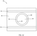
FIG. 12 is a top view of a structure in accordance with alternative embodiments of the invention. - With reference to
FIGS. 1, 2 and in accordance with embodiments of the invention, astructure 10 for a directional coupler includes awaveguide core 12 and awaveguide core 14 that are positioned on, and over, adielectric layer 16 and asemiconductor substrate 18. In an embodiment, thedielectric layer 16 may be comprised of a dielectric material, such as silicon dioxide, and thesemiconductor substrate 18 may be comprised of a semiconductor material, such as single-crystal silicon. In an embodiment, thedielectric layer 16 may be a buried oxide layer of a silicon-on-insulator substrate, and thedielectric layer 16 may be disposed between thewaveguide cores semiconductor substrate 18. Thedielectric layer 16 may function as an underlying cladding layer for thewaveguide cores - The
waveguide core 12 includesmultiple segments 30 that are distributed in aninput region 20, acoupling region 22, and anoutput region 24. Thesegments 30 are positioned in a spaced-apart arrangement in which spaces or gaps G1 alternate with thesegments 30. In thecoupling region 22, thesegments 30 alternate with the gaps G1 along thelongitudinal axis 32. In theinput region 20 and theoutput region 24, thesegments 30 may be arranged with curved routing that approximates respective bends. In an embodiment, the pitch and duty cycle of thesegments 30 may be uniform to define a periodic arrangement. In alternative embodiments, the pitch and/or the duty cycle of thesegments 30 may be apodized (i.e., non-uniform) to define a non-periodic arrangement. In an alternative embodiment, a rib may be overlaid with some or all of thesegments 30. - The
waveguide core 14 includesmultiple segments 34 that are distributed in theinput region 20, thecoupling region 22, and theoutput region 24. Thesegments 34 are positioned in a spaced-apart arrangement in which spaces or gaps G2 alternate with thesegments 34. In thecoupling region 22, thesegments 34 and the gaps G2 alternate along thelongitudinal axis 36. In theinput region 20 and theoutput region 24, thesegments 34 may be arranged with curved routing that approximates respective bends. In an embodiment, the pitch and duty cycle of thesegments 34 may be uniform to define a periodic arrangement. In alternative embodiments, the pitch and/or the duty cycle of thesegments 34 may be apodized (i.e., non-uniform) to define a non-periodic arrangement. In an alternative embodiment, a rib may be overlaid with some or all of thesegments 34. - Each
segment 30 has asidewall 26, asidewall 27 opposite to thesidewall 26, abottom surface 23 adjacent to thedielectric layer 16, and atop surface 25 opposite to thebottom surface 23. Thesidewalls bottom surface 23 to thetop surface 25. Eachsegment 34 has asidewall 28, asidewall 29 opposite to thesidewall 28, abottom surface 31 adjacent to thedielectric layer 16, and atop surface 33 opposite to thebottom surface 31. Thesidewalls bottom surface 31 to thetop surface 33. - The
segments 30 of thewaveguide core 12 may be spaced from thesegments 34 of thewaveguide core 14 by a gap G3 in thecoupling region 22. More specifically, thesegments 30 and thesegments 34 may be arranged in thecoupling region 22 such that thesidewall 26 of eachsegment 30 is disposed across the gap G3 from thesidewall 28 of one of thesegments 34. In an embodiment, thelongitudinal axis 32 may be arranged parallel to thelongitudinal axis 36 in thecoupling region 22. In an embodiment, thesegments 30 and thesegments 34 may be characterized by the same pitch and/or duty cycle. In an embodiment, thesegments 30 may be characterized by a different pitch and/or duty cycle than thesegments 34. In an embodiment, thesegments 30 may have a width in a direction transverse to thelongitudinal axis 32, thesegments 34 may have a width in a direction transverse to thelongitudinal axis 36, and the width of thesegments 30 may be equal to the width of thesegments 34. In an embodiment, thesegments 30 may have a width transverse to thelongitudinal axis 32, thesegments 34 may have a width in a direction transverse to thelongitudinal axis 36, and the width of thesegments 30 may be unequal to the width of thesegments 34. Thesegments 30 are spaced from thesegments 34 by a distance greater than the gap G3 in theinput region 20 and in theoutput region 24. - In an embodiment, the
waveguide cores waveguide cores waveguide cores waveguide cores waveguide cores - In an embodiment, the
waveguide cores waveguide cores waveguide cores segments waveguide cores waveguide cores segments 30 and less than the thickness of thesegments 34. - With reference to
FIGS. 3 ,4, 4A in which like reference numerals refer to like features inFIGS. 1, 2 and at a subsequent fabrication stage, acladding layer 38 may be disposed between thewaveguide core 12 and thewaveguide core 14 in thecoupling region 22. In particular, thecladding layer 38 may be disposed inside the gaps G3 between thesegments 30 of thewaveguide core 12 and thesegments 34 of thewaveguide core 14. The material of thecladding layer 38 may adjoin theinner sidewall 26 of eachsegment 30, and the material of thecladding layer 38 may adjoin theinner sidewall 28 of eachsegment 34. Thecladding layer 38 may also disposed in the space between thesegments 30 and thesegments 34 in theinput region 20 and the space between thesegments 30 and thesegments 34 in theoutput region 24. Thecladding layer 38 may be deposited and planarized after deposition, and then patterned with lithography and etching processes. - A
cladding layer 40 may be disposed inside the gaps G1 between thesegments 30 of thewaveguide core 12 and the gaps G2 between thesegments 34 of thewaveguide core 14, as well as in the space between thesegments 30 in theinput region 20 and thesegments 30 in theoutput region 24 and in the space between thesegments 34 in theinput region 20 and thesegments 34 in theoutput region 24. The material of thecladding layer 40 may adjoin theouter sidewall 27 of eachsegment 30, and the material of thecladding layer 40 may adjoin theouter sidewall 29 of eachsegment 34. Thecladding layer 40 may be deposited and planarized after deposition, and then patterned with lithography and etching processes. - In an embodiment, the
cladding layer 38 may be deposited and patterned before depositing thecladding layer 40, the gaps G1 and the gaps G2 may be unfilled following the patterning of thecladding layer 38, and the material of the subsequently-depositedcladding layer 40 may fill the gaps G1 and the gaps G2. In an alternative embodiment, thecladding layer 40 may be deposited and patterned before depositing thecladding layer 38, the gap G3 may be unfilled following the patterning of thecladding layer 40, and the material of the subsequently-depositedcladding layer 38 may fill the gap G3. - The
cladding layer 38 may be comprised of a material having a refractive index that is less than the refractive index of the material constituting thewaveguide cores cladding layer 40 may also be comprised of a material having a refractive index that is less than the refractive index of the material constituting thewaveguide cores cladding layer 40 may be different from the refractive index of the of thecladding layer 38. In an embodiment, the refractive index of the material of thecladding layer 40 may be less than the refractive index of the material of thecladding layer 38. In an embodiment, the refractive index of the material of thecladding layer 40 may be greater than the refractive index of the material of thecladding layer 38. In an embodiment, the cladding layers 38, 40 may be dielectric materials selected from silicon nitride, aluminum nitride, silicon oxynitride, diamond, aluminum oxide, calcium fluoride, carbon-doped silicon oxide, tetraethylorthosilicate silicon dioxide, fluorinated-tetraethylorthosilicate silicon dioxide, and magnesium fluoride. In an embodiment, thecladding layer 38 may be comprised of silicon nitride, and thecladding layer 40 may be comprised of silicon dioxide. In an embodiment, the cladding layers 38, 40 may be comprised of respective non-ferroelectric materials with different refractive indices. - In an embodiment, the
cladding layer 38 and thecladding layer 40 may have equal thicknesses. In an embodiment, thecladding layer 38 and thecladding layer 40 may have unequal thicknesses. In an embodiment, thecladding layer 38 may be thicker than thecladding layer 40. In an embodiment, thecladding layer 38 may be thinner than thecladding layer 40. In an embodiment, thecladding layer 38 and/or thecladding layer 40 may have respective thicknesses that are equal to the thicknesses of thesegments cladding layer 38 and/or thecladding layer 40 may have respective thicknesses that are not equal to the thicknesses of thesegments - In an embodiment, the dielectric material of the
dielectric layer 16 may have a refractive index that is equal or substantially equal to the refractive index of the material of thecladding layer 38. In an embodiment, the dielectric material of thedielectric layer 16 may have a refractive index that is equal or substantially equal to the refractive index of the material of thecladding layer 40. In an embodiment, the dielectric material of thedielectric layer 16 may have a refractive index that is different from the refractive index of the material of thecladding layer 38 and/or different from the refractive index of the material of thecladding layer 40. - In an embodiment, the
segments 30 of thewaveguide core 12 may be dimensioned and positioned at small enough pitch so as to define a sub-wavelength grating that does not radiate or reflect light at a wavelength of operation, and thesegments 34 of thewaveguide core 14 may be dimensioned and positioned at small enough pitch so as to define a sub-wavelength grating that does not radiate or reflect light at a wavelength of operation. The material of thecladding layer 40 is disposed in the gaps G1 between adjacent pairs of thesegments 30 such that a metamaterial structure is defined in which the material constituting thesegments 30 has a higher refractive index than the material of thecladding layer 40. The material of thecladding layer 40 is disposed in the gaps G2 between adjacent pairs of thesegments 34 such that a metamaterial structure is defined in which the material constituting thesegments 34 has a higher refractive index than the material of thecladding layer 40. Each metamaterial structure can be treated as a homogeneous material having an effective refractive index that is intermediate between the refractive index of the material constituting thesegments cladding layer 40. - With reference to
FIGS. 5, 5A in which like reference numerals refer to like features inFIGS. 4, 4A and at a subsequent fabrication stage, a dielectric layer 42 is formed on, and over, thewaveguide cores waveguide cores cladding layer 38. In an embodiment, the dielectric material of the dielectric layer 42 may have a refractive index that is equal or substantially equal to the refractive index of the material of thecladding layer 40. In an embodiment, the dielectric material of the dielectric layer 42 may have a refractive index that is different from the refractive index of the material of thecladding layer 38 and/or different from the refractive index of the material of thecladding layer 40. The dielectric layer 42 may be disposed on thetop surface 25 of eachsegment 30 and thetop surface 33 of eachsegment 30, and the dielectric layer 42 may function as an overlying cladding layer for thewaveguide cores - In use, light (e.g., laser light) may be guided on a photonics chip by the
waveguide core 12 to theinput region 20 of the directional coupler. In thecoupling region 22, all or a portion of the arriving light is transferred in a lateral direction from thesegments 30 of thewaveguide core 12 to thesegments 34 of thewaveguide core 14. Light may exit the directional coupler via thewaveguide core 12 and thewaveguide core 14 in theoutput region 24. - The
waveguide core 12 and thewaveguide core 14 define a directional coupler that includes inhomogeneous or heterogenous lateral claddings supplied by thecladding layer 38 and thecladding layer 40 that are comprised materials of different refractive index. The heterogenous lateral claddings of different refractive index may permit the dimension of the gap G3 between thesegments 30 of thewaveguide core 12 and thesegments 34 of thewaveguide core 14 in thecoupling region 22 to be increased without reducing the coupling strength and may also permit a significant reduction in the device footprint. As a result of the relaxation on the restriction on the dimension of the gap G3, thecladding layer 38 may be deposited with a significantly reduced risk of forming air voids in the gap G3. - With reference to
FIGS. 6 ,7, 7A and in accordance with alternative embodiments, thecladding layer 38 may be disposed inside the gaps G1 between thesegments 30 of thewaveguide core 12 and the gaps G2 between thesegments 34 of thewaveguide core 14 instead of thecladding layer 40. Thecladding layer 38 is disposed in the space between thesegments 30 in theinput region 20 and thesegments 30 in theoutput region 24 and in the space between thesegments 34 in theinput region 20 and thesegments 34 in theoutput region 24. The material of thecladding layer 38 may also adjoin theinner sidewall 26 of eachsegment 30, and the material of thecladding layer 38 may also adjoin theinner sidewall 28 of eachsegment 34. The material of thecladding layer 40 may adjoin theouter sidewall 27 of eachsegment 30, and the material of thecladding layer 40 may adjoin theouter sidewall 29 of eachsegment 34. - With reference to
FIG. 8 and in accordance with alternative embodiments, astructure 70 may includewaveguide cores input region 20, thecoupling region 22, and theoutput region 24. Thewaveguide core 12 has asidewall 62 and asidewall 64 opposite to thesidewall 62, and thewaveguide core 14 has asidewall 66 and asidewall 68 opposite to thesidewall 66. Thecladding layer 38 is disposed in thecoupling region 22 inside the gap G3 between thesidewall 62 of thewaveguide core 12 and thesidewall 66 of thewaveguide core 14, as well as in the space between thewaveguide core 12 and thewaveguide core 14 in theinput region 20 and in the space between thewaveguide core 12 and thewaveguide core 14 in theoutput region 24. In an alternative embodiment, thewaveguide cores cladding layer 40 may be disposed inside the slots. - With reference to
FIG. 9 and in accordance with alternative embodiments, thestructure 70 may include the material of both cladding layers 38, 40 inside the gap G3 over thecoupling region 22. Specifically, sections of thecladding layer 40 may alternate with sections of thecladding layer 38 to define a grating-like arrangement inside the gap G3 over the length of thecoupling region 22. The sections of each of the cladding layers 38, 40 may be defined when patterning the respective deposited layers. In an embodiment, the sections of thecladding layer 38 and the sections of thecladding layer 40 may be arranged to define a sub-wavelength grating inside the gap G3. - With reference to
FIG. 10 ,11, 11A and in accordance with alternative embodiments, the material of thecladding layer 40 may be disposed in the gaps G1 between adjacent pairs of thesegments 30 in thecoupling region 22 and in the gaps G2 between adjacent pairs of thesegments 34 in thecoupling region 22. The material of thecladding layer 38 may be disposed in the portions of the gap G3 between thesidewalls 26 of thesegments 30 and thesidewalls 28 of thesegments 34 that are arranged across the gap G3 from each other. As a result, the materials inside the gap G3 have refractive indices that alternate along the length of thecoupling region 22 of thestructure 10. - With reference to
FIG. 12 and in accordance with alternative embodiments, astructure 50 for a directional coupler may include awaveguide core 52, awaveguide core 54 and aring resonator 56 positioned adjacent to respective portions of thewaveguide cores ring resonator 56 may be positioned adjacent to thewaveguide core 52 with a gap separating thering resonator 56 from the portion of thewaveguide core 52, and thering resonator 56 may be positioned adjacent to thewaveguide core 54 with a gap separating thering resonator 56 from the portion of thewaveguide core 54. In an embodiment, thering resonator 56 may be a waveguide core that is shaped as a closed loop or ring. Thewaveguide core 52 may serve as an input bus, and thewaveguide core 54 may serve as an output bus. Thering resonator 56 may have an inner ring-shapededge 58 defining an inner diameter and an outer ring-shapededge 60 defining an outer diameter. - In an embodiment, the
cladding layer 38 may be formed inside the inner ring-shapededge 58 of thering resonator 56, and thecladding layer 40 may be formed outside the outer ring-shapededge 60 of thering resonator 56. In an alternative embodiment, the waveguide core of thering resonator 56 may be divided into segments, the segments may be arranged within the ring shape to define a sub-wavelength grating, and either the material of thecladding layer 38 or the material of thecladding layer 40 may be arranged in the gaps between the segments. In an embodiment, thewaveguide cores ring resonator 56 may be comprised of the same material, such as silicon. In an alternative embodiment, an additional ring resonator may be positioned between thewaveguide cores ring resonator 56. - In use, light (e.g., laser light) may be coupled and transferred in a lateral direction from the
waveguide core 52 to thering resonator 56. The light may be subsequently coupled and transferred in a lateral direction from thering resonator 56 to thewaveguide core 54. The result is light transfer from thewaveguide core 52 to thewaveguide core 54. - The methods as described above are used in the fabrication of integrated circuit chips. The resulting integrated circuit chips can be distributed by the fabricator in raw wafer form (e.g., as a single wafer that has multiple unpackaged chips), as a bare die, or in a packaged form. The chip may be integrated with other chips, discrete circuit elements, and/or other signal processing devices as part of either an intermediate product or an end product. The end product can be any product that includes integrated circuit chips, such as computer products having a central processor or smartphones.
- References herein to terms modified by language of approximation, such as "about", "approximately", and "substantially", are not to be limited to the precise value specified. The language of approximation may correspond to the precision of an instrument used to measure the value and, unless otherwise dependent on the precision of the instrument, may indicate a range of +/- 10% of the stated value(s).
- References herein to terms such as "vertical", "horizontal", etc. are made by way of example, and not by way of limitation, to establish a frame of reference. The term "horizontal" as used herein is defined as a plane parallel to a conventional plane of a semiconductor substrate, regardless of its actual three-dimensional spatial orientation. The terms "vertical" and "normal" refer to a direction in the frame of reference perpendicular to the horizontal, as just defined. The term "lateral" refers to a direction in the frame of reference within the horizontal plane.
- A feature "connected" or "coupled" to or with another feature may be directly connected or coupled to or with the other feature or, instead, one or more intervening features may be present. A feature may be "directly connected" or "directly coupled" to or with another feature if intervening features are absent. A feature may be "indirectly connected" or "indirectly coupled" to or with another feature if at least one intervening feature is present. A feature "on" or "contacting" another feature may be directly on or in direct contact with the other feature or, instead, one or more intervening features may be present. A feature may be "directly on" or in "direct contact" with another feature if intervening features are absent. A feature may be "indirectly on" or in "indirect contact" with another feature if at least one intervening feature is present. Different features may "overlap" if a feature extends over, and covers a part of, another feature with either direct contact or indirect contact.
- The descriptions of the various embodiments of the present invention have been presented for purposes of illustration but are not intended to be exhaustive or limited to the embodiments disclosed. Many modifications and variations will be apparent to those of ordinary skill in the art without departing from the scope and spirit of the described embodiments. The terminology used herein was chosen to best explain the principles of the embodiments, the practical application or technical improvement over technologies found in the marketplace, or to enable others of ordinary skill in the art to understand the embodiments disclosed herein.
Claims (15)
- A structure for a directional coupler, the structure comprising:a first waveguide core including a first plurality of segments arranged along a first longitudinal axis, each of the first plurality of segments having a first sidewall and a second sidewall opposite to the first sidewall;a second waveguide core including a second plurality of segments arranged along a second longitudinal axis, each of the second plurality of segments having a first sidewall and a second sidewall opposite to the first sidewall, and the first sidewall of each of the second plurality of segments adjacent to the first sidewall of one of the first plurality of segments in a coupling region;a first cladding layer comprising a first material that has a first refractive index, the first cladding layer adjoining the first sidewall of each of the first plurality of segments and the first sidewall of each of the second plurality of segments; anda second cladding layer comprising a second material that has a second refractive index different from the first refractive index, the second cladding layer adjoining the second sidewall of each of the first plurality of segments and the second sidewall of each of the second plurality of segments.
- The structure of claim 1 wherein the second refractive index is greater than the first refractive index, or wherein the second refractive index is less than the first refractive index.
- The structure of claim 1 or claim 2 wherein the first waveguide core includes a first plurality of gaps that alternate with the first plurality of segments along the first longitudinal axis, the second waveguide core includes a second plurality of gaps that alternate with the second plurality of segments along the second longitudinal axis, and the first cladding layer is disposed in the first plurality of gaps and the second plurality of gaps.
- The structure of claim 1 or claim 2 wherein the first waveguide core includes a first plurality of gaps that alternate with the first plurality of segments along the first longitudinal axis, the second waveguide core includes a second plurality of gaps that alternate with the first plurality of segments along the second longitudinal axis, and the second cladding layer is disposed in the first plurality of gaps and the second plurality of gaps.
- The structure of one of claims 1 to 4 wherein each of the first plurality of segments has a bottom surface, each of the second plurality of segments has a bottom surface, and further comprising:a dielectric layer comprised of a dielectric material,wherein the bottom surface of each of the first plurality of segments is disposed on the dielectric layer, and the bottom surface of each of the second plurality of segments is disposed on the dielectric layer.
- The structure of claim 5 wherein the dielectric material has a third refractive index that is different from the first refractive index, and/or wherein the first cladding layer and the second cladding layer are disposed on the dielectric layer.
- The structure of one of claims 1 to 6 wherein each of the first plurality of segments has a top surface, each of the second plurality of segments has a top surface, and further comprising:a dielectric layer comprised of a dielectric material,wherein the dielectric layer is disposed on the top surface of each of the first plurality of segments, and the dielectric layer is disposed on the top surface of each of the second plurality of segments.
- The structure of claim 7 wherein the dielectric material has a third refractive index that is different from the first refractive index, and/or wherein the dielectric layer is disposed on the first cladding layer and the second cladding layer.
- The structure of one of claims 1 to 8 wherein the first material comprises a first non-ferroelectric material, and the second material comprises a second non-ferroelectric material, or wherein the first material comprises a silicon nitride, and the second material comprises silicon dioxide.
- A structure for a directional coupler, the structure comprising:a first waveguide core having a first sidewall and a second sidewall opposite to the first sidewall;a second waveguide core having a first sidewall and a second sidewall opposite to the first sidewall, the first sidewall of the second waveguide core spaced from the first sidewall of the first waveguide core by a gap in a coupling region;a first cladding layer comprising a first material having a first refractive index, the first cladding layer including a first plurality of sections in the gap; anda second cladding layer comprising a second material that has a second refractive index different from the first refractive index, the second cladding layer including a second plurality of sections in the gap, and the second plurality of sections of the second cladding layer alternating with the first plurality of sections of the first cladding layer.
- The structure of claim 10 wherein the second cladding layer is disposed adjacent to the second sidewall of the first waveguide core, and the second cladding layer is disposed adjacent to the second sidewall of the second waveguide core.
- The structure of claim 10 or claim 11 wherein the second refractive index is greater than the first refractive index, or wherein the second refractive index is less than the first refractive index.
- The structure of one of claims 10 to 12 wherein the first plurality of sections of the first cladding layer and the second plurality of sections of the second cladding layer define a sub-wavelength grating.
- The structure of one of claims 10 to 13 wherein the first material comprises a first non-ferroelectric material, and the second material comprises a second non-ferroelectric material.
- A method of forming a structure for a directional coupler, the method comprising:forming a first waveguide core including a first plurality of segments arranged along a first longitudinal axis, wherein each of the first plurality of segments has a first sidewall and a second sidewall opposite to the first sidewall;forming a second waveguide core including a second plurality of segments arranged along a second longitudinal axis, wherein each of the second plurality of segments has a first sidewall and a second sidewall opposite to the first sidewall, and the first sidewall of each of the second plurality of segments is disposed adjacent to the first sidewall of one of the first plurality of segments in a coupling region;forming a first cladding layer comprising a first material having a first refractive index, wherein the first cladding layer adjoins the first sidewall of each of the first plurality of segments and the first sidewall of each of the second plurality of segments; andforming a second cladding layer comprising a second material that has a second refractive index different from the first refractive index, wherein the second cladding layer adjoins the second sidewall of each of the first plurality of segments and the second sidewall of each of the second plurality of segments.
Applications Claiming Priority (1)
| Application Number | Priority Date | Filing Date | Title |
|---|---|---|---|
| US18/096,607 US12449599B2 (en) | 2023-01-13 | 2023-01-13 | Directional couplers with heterogenous claddings |
Publications (4)
| Publication Number | Publication Date |
|---|---|
| EP4400883A2 true EP4400883A2 (en) | 2024-07-17 |
| EP4400883A3 EP4400883A3 (en) | 2024-10-02 |
| EP4400883B1 EP4400883B1 (en) | 2025-08-06 |
| EP4400883C0 EP4400883C0 (en) | 2025-08-06 |
Family
ID=88510871
Family Applications (1)
| Application Number | Title | Priority Date | Filing Date |
|---|---|---|---|
| EP23205378.5A Active EP4400883B1 (en) | 2023-01-13 | 2023-10-24 | Directional couplers with heterogenous claddings |
Country Status (3)
| Country | Link |
|---|---|
| US (1) | US12449599B2 (en) |
| EP (1) | EP4400883B1 (en) |
| CN (1) | CN118348634A (en) |
Families Citing this family (2)
| Publication number | Priority date | Publication date | Assignee | Title |
|---|---|---|---|---|
| US12572050B2 (en) * | 2023-07-11 | 2026-03-10 | Taiwan Semiconductor Manufacturing Company, Ltd. | Semiconductor device including optical ring waveguide |
| US20250102302A1 (en) * | 2023-09-27 | 2025-03-27 | Honeywell International Inc. | Directional coupler with reduced phase distortion |
Family Cites Families (18)
| Publication number | Priority date | Publication date | Assignee | Title |
|---|---|---|---|---|
| US4483583A (en) * | 1981-03-07 | 1984-11-20 | Licentia Patent-Verwaltungs-Gmbh | Selective directional coupler for guided waves |
| CA2153595A1 (en) * | 1993-01-11 | 1994-07-21 | Anthony F. Garito | Polycyclic aromatic compounds having nonlinear optical properties |
| US5715337A (en) * | 1996-09-19 | 1998-02-03 | The Mirco Optical Corporation | Compact display system |
| WO2001040836A1 (en) * | 1999-12-02 | 2001-06-07 | Gemfire Corporation | Photodefinition of optical devices |
| WO2003102648A2 (en) * | 2002-06-04 | 2003-12-11 | Nkt Integration A/S | Integrated splitter with reduced losses |
| FR2841658B1 (en) * | 2002-06-26 | 2004-10-22 | Centre Nat Rech Scient | WAVELENGTH SELECTIVE AND DIRECTIONAL OPTICAL COUPLING DEVICE |
| EP1543362A1 (en) * | 2002-09-27 | 2005-06-22 | Pirelli & C. S.p.A. | Integrated optical device |
| JP4636439B2 (en) | 2005-11-30 | 2011-02-23 | 日立化成工業株式会社 | Calculation method of core width and distance between cores of two linear optical waveguides of directional optical coupler |
| JP5262639B2 (en) * | 2008-12-03 | 2013-08-14 | 沖電気工業株式会社 | Optical element and Mach-Zehnder interferometer |
| JP6492437B2 (en) | 2014-07-22 | 2019-04-03 | 沖電気工業株式会社 | Directional coupler and design method thereof, optical waveguide device, and wavelength filter |
| US9563016B1 (en) * | 2015-11-24 | 2017-02-07 | Omega Optics, Inc. | Subwavelength photonic crystal waveguide with trapezoidal shaped dielectric pillars in optical systems |
| US10585254B2 (en) * | 2017-11-17 | 2020-03-10 | Samsung Electronics Co., Ltd. | Vertical optical via and method of fabrication |
| EP3705918B1 (en) * | 2019-03-08 | 2025-04-30 | Infineon Technologies AG | BANDPASS TRANSMISSION FILTER AND NARROWBAND RADIATION SOURCE |
| US10795083B1 (en) | 2019-05-30 | 2020-10-06 | Globalfoundries Inc. | Heterogeneous directional couplers for photonics chips |
| US11150407B2 (en) * | 2020-03-17 | 2021-10-19 | Globalfoundries U.S. Inc. | Optical couplers with non-linear tapering |
| US10983273B1 (en) * | 2020-06-22 | 2021-04-20 | Voyant Photonics, Inc. | Integrated optical waveguide emitter |
| US11480729B2 (en) * | 2020-10-30 | 2022-10-25 | Nokia Solutions And Networks Oy | Thermally compensated slot waveguide |
| US11768337B2 (en) | 2021-06-29 | 2023-09-26 | Globalfoundries U.S. Inc. | Couplers including a waveguide core with integrated airgaps |
-
2023
- 2023-01-13 US US18/096,607 patent/US12449599B2/en active Active
- 2023-10-24 EP EP23205378.5A patent/EP4400883B1/en active Active
- 2023-10-31 CN CN202311425575.3A patent/CN118348634A/en active Pending
Also Published As
| Publication number | Publication date |
|---|---|
| US20240241314A1 (en) | 2024-07-18 |
| US12449599B2 (en) | 2025-10-21 |
| CN118348634A (en) | 2024-07-16 |
| EP4400883B1 (en) | 2025-08-06 |
| EP4400883C0 (en) | 2025-08-06 |
| EP4400883A3 (en) | 2024-10-02 |
Similar Documents
| Publication | Publication Date | Title |
|---|---|---|
| US10816726B1 (en) | Edge couplers for photonics applications | |
| US11467341B2 (en) | Waveguide crossings including a segmented waveguide section | |
| EP4400883B1 (en) | Directional couplers with heterogenous claddings | |
| US11092740B1 (en) | Polarizers with multiple stacked layers | |
| US11275207B2 (en) | Multimode waveguide bends with features to reduce bending loss | |
| US10795082B1 (en) | Bragg gratings with airgap cladding | |
| US11150407B2 (en) | Optical couplers with non-linear tapering | |
| US20220326434A1 (en) | Optical components with power-handling assistance | |
| US11256030B1 (en) | Optical power splitters including a non-linear waveguide taper | |
| EP4343394A1 (en) | Optical couplers for transitioning between a single-layer waveguide and a multiple-layer waveguide | |
| US11269142B2 (en) | Optical couplers with segmented waveguides | |
| EP4455746B1 (en) | Reference markers adjacent to a cavity in a photonics chip | |
| CN115113326A (en) | Optical coupler for ridge to rib waveguide core transition | |
| KR102891313B1 (en) | Edge couplers including a metamaterial layer | |
| EP4400880A1 (en) | Optical components with one or more embedded bragg reflectors | |
| EP4372426A1 (en) | Optical components with an adjacent metamaterial structure | |
| US20230143832A1 (en) | Optical couplers with diagonal light transfer | |
| EP4310561A1 (en) | Waveguide crossings with a multiple-level non-contacting arrangement | |
| EP4286904A1 (en) | Multiple-tip edge couplers with segmented waveguide cores | |
| EP4220257B1 (en) | Multiple-core heterogeneous waveguide structures including multiple slots | |
| US12092868B2 (en) | Photonics chips with reticle stitching by side-by-side tapered sections | |
| EP4418027A1 (en) | Optical power splitters incorporating one or more spiral elements | |
| US12449597B2 (en) | Edge couplers with coupling-assisting features |
Legal Events
| Date | Code | Title | Description |
|---|---|---|---|
| PUAI | Public reference made under article 153(3) epc to a published international application that has entered the european phase |
Free format text: ORIGINAL CODE: 0009012 |
|
| STAA | Information on the status of an ep patent application or granted ep patent |
Free format text: STATUS: THE APPLICATION HAS BEEN PUBLISHED |
|
| AK | Designated contracting states |
Kind code of ref document: A2 Designated state(s): AL AT BE BG CH CY CZ DE DK EE ES FI FR GB GR HR HU IE IS IT LI LT LU LV MC ME MK MT NL NO PL PT RO RS SE SI SK SM TR |
|
| PUAL | Search report despatched |
Free format text: ORIGINAL CODE: 0009013 |
|
| AK | Designated contracting states |
Kind code of ref document: A3 Designated state(s): AL AT BE BG CH CY CZ DE DK EE ES FI FR GB GR HR HU IE IS IT LI LT LU LV MC ME MK MT NL NO PL PT RO RS SE SI SK SM TR |
|
| RIC1 | Information provided on ipc code assigned before grant |
Ipc: G02B 6/12 20060101ALI20240827BHEP Ipc: G02B 6/125 20060101AFI20240827BHEP |
|
| STAA | Information on the status of an ep patent application or granted ep patent |
Free format text: STATUS: REQUEST FOR EXAMINATION WAS MADE |
|
| 17P | Request for examination filed |
Effective date: 20241015 |
|
| RBV | Designated contracting states (corrected) |
Designated state(s): AL AT BE BG CH CY CZ DE DK EE ES FI FR GB GR HR HU IE IS IT LI LT LU LV MC ME MK MT NL NO PL PT RO RS SE SI SK SM TR |
|
| GRAP | Despatch of communication of intention to grant a patent |
Free format text: ORIGINAL CODE: EPIDOSNIGR1 |
|
| STAA | Information on the status of an ep patent application or granted ep patent |
Free format text: STATUS: GRANT OF PATENT IS INTENDED |
|
| GRAJ | Information related to disapproval of communication of intention to grant by the applicant or resumption of examination proceedings by the epo deleted |
Free format text: ORIGINAL CODE: EPIDOSDIGR1 |
|
| STAA | Information on the status of an ep patent application or granted ep patent |
Free format text: STATUS: REQUEST FOR EXAMINATION WAS MADE |
|
| INTG | Intention to grant announced |
Effective date: 20250430 |
|
| RIN1 | Information on inventor provided before grant (corrected) |
Inventor name: BIAN, YUSHENG |
|
| GRAS | Grant fee paid |
Free format text: ORIGINAL CODE: EPIDOSNIGR3 |
|
| STAA | Information on the status of an ep patent application or granted ep patent |
Free format text: STATUS: GRANT OF PATENT IS INTENDED |
|
| GRAP | Despatch of communication of intention to grant a patent |
Free format text: ORIGINAL CODE: EPIDOSNIGR1 |
|
| GRAA | (expected) grant |
Free format text: ORIGINAL CODE: 0009210 |
|
| STAA | Information on the status of an ep patent application or granted ep patent |
Free format text: STATUS: THE PATENT HAS BEEN GRANTED |
|
| INTC | Intention to grant announced (deleted) | ||
| INTG | Intention to grant announced |
Effective date: 20250626 |
|
| AK | Designated contracting states |
Kind code of ref document: B1 Designated state(s): AL AT BE BG CH CY CZ DE DK EE ES FI FR GB GR HR HU IE IS IT LI LT LU LV MC ME MK MT NL NO PL PT RO RS SE SI SK SM TR |
|
| REG | Reference to a national code |
Ref country code: GB Ref legal event code: FG4D |
|
| REG | Reference to a national code |
Ref country code: CH Ref legal event code: EP |
|
| REG | Reference to a national code |
Ref country code: DE Ref legal event code: R096 Ref document number: 602023005443 Country of ref document: DE |
|
| REG | Reference to a national code |
Ref country code: IE Ref legal event code: FG4D |
|
| U01 | Request for unitary effect filed |
Effective date: 20250806 |
|
| U07 | Unitary effect registered |
Designated state(s): AT BE BG DE DK EE FI FR IT LT LU LV MT NL PT RO SE SI Effective date: 20250813 |
|
| U20 | Renewal fee for the european patent with unitary effect paid |
Year of fee payment: 3 Effective date: 20250922 |
|
| PG25 | Lapsed in a contracting state [announced via postgrant information from national office to epo] |
Ref country code: IS Free format text: LAPSE BECAUSE OF FAILURE TO SUBMIT A TRANSLATION OF THE DESCRIPTION OR TO PAY THE FEE WITHIN THE PRESCRIBED TIME-LIMIT Effective date: 20251206 |
|
| PG25 | Lapsed in a contracting state [announced via postgrant information from national office to epo] |
Ref country code: NO Free format text: LAPSE BECAUSE OF FAILURE TO SUBMIT A TRANSLATION OF THE DESCRIPTION OR TO PAY THE FEE WITHIN THE PRESCRIBED TIME-LIMIT Effective date: 20251106 |
|
| PG25 | Lapsed in a contracting state [announced via postgrant information from national office to epo] |
Ref country code: HR Free format text: LAPSE BECAUSE OF FAILURE TO SUBMIT A TRANSLATION OF THE DESCRIPTION OR TO PAY THE FEE WITHIN THE PRESCRIBED TIME-LIMIT Effective date: 20250806 |
|
| PG25 | Lapsed in a contracting state [announced via postgrant information from national office to epo] |
Ref country code: GR Free format text: LAPSE BECAUSE OF FAILURE TO SUBMIT A TRANSLATION OF THE DESCRIPTION OR TO PAY THE FEE WITHIN THE PRESCRIBED TIME-LIMIT Effective date: 20251107 |
|
| PG25 | Lapsed in a contracting state [announced via postgrant information from national office to epo] |
Ref country code: PL Free format text: LAPSE BECAUSE OF FAILURE TO SUBMIT A TRANSLATION OF THE DESCRIPTION OR TO PAY THE FEE WITHIN THE PRESCRIBED TIME-LIMIT Effective date: 20250806 |
|
| PG25 | Lapsed in a contracting state [announced via postgrant information from national office to epo] |
Ref country code: RS Free format text: LAPSE BECAUSE OF FAILURE TO SUBMIT A TRANSLATION OF THE DESCRIPTION OR TO PAY THE FEE WITHIN THE PRESCRIBED TIME-LIMIT Effective date: 20251106 |
|
| PG25 | Lapsed in a contracting state [announced via postgrant information from national office to epo] |
Ref country code: ES Free format text: LAPSE BECAUSE OF FAILURE TO SUBMIT A TRANSLATION OF THE DESCRIPTION OR TO PAY THE FEE WITHIN THE PRESCRIBED TIME-LIMIT Effective date: 20250806 |
|
| PG25 | Lapsed in a contracting state [announced via postgrant information from national office to epo] |
Ref country code: SM Free format text: LAPSE BECAUSE OF FAILURE TO SUBMIT A TRANSLATION OF THE DESCRIPTION OR TO PAY THE FEE WITHIN THE PRESCRIBED TIME-LIMIT Effective date: 20250806 |
|
| PG25 | Lapsed in a contracting state [announced via postgrant information from national office to epo] |
Ref country code: CZ Free format text: LAPSE BECAUSE OF FAILURE TO SUBMIT A TRANSLATION OF THE DESCRIPTION OR TO PAY THE FEE WITHIN THE PRESCRIBED TIME-LIMIT Effective date: 20250806 |
|
| PG25 | Lapsed in a contracting state [announced via postgrant information from national office to epo] |
Ref country code: SK Free format text: LAPSE BECAUSE OF FAILURE TO SUBMIT A TRANSLATION OF THE DESCRIPTION OR TO PAY THE FEE WITHIN THE PRESCRIBED TIME-LIMIT Effective date: 20250806 |
|
| PLBE | No opposition filed within time limit |
Free format text: ORIGINAL CODE: 0009261 |
|
| STAA | Information on the status of an ep patent application or granted ep patent |
Free format text: STATUS: NO OPPOSITION FILED WITHIN TIME LIMIT |
|
| REG | Reference to a national code |
Ref country code: CH Ref legal event code: L10 Free format text: ST27 STATUS EVENT CODE: U-0-0-L10-L00 (AS PROVIDED BY THE NATIONAL OFFICE) Effective date: 20260617 |
|
| PG25 | Lapsed in a contracting state [announced via postgrant information from national office to epo] |
Ref country code: MC Free format text: LAPSE BECAUSE OF FAILURE TO SUBMIT A TRANSLATION OF THE DESCRIPTION OR TO PAY THE FEE WITHIN THE PRESCRIBED TIME-LIMIT Effective date: 20250806 |
|
| 26N | No opposition filed |
Effective date: 20260507 |