EP4400880A1 - Optical components with one or more embedded bragg reflectors - Google Patents
Optical components with one or more embedded bragg reflectors Download PDFInfo
- Publication number
- EP4400880A1 EP4400880A1 EP23204229.1A EP23204229A EP4400880A1 EP 4400880 A1 EP4400880 A1 EP 4400880A1 EP 23204229 A EP23204229 A EP 23204229A EP 4400880 A1 EP4400880 A1 EP 4400880A1
- Authority
- EP
- European Patent Office
- Prior art keywords
- waveguide core
- tapered section
- waveguide
- segments
- slab region
- Prior art date
- Legal status (The legal status is an assumption and is not a legal conclusion. Google has not performed a legal analysis and makes no representation as to the accuracy of the status listed.)
- Pending
Links
Images



Classifications
-
- G—PHYSICS
- G02—OPTICS
- G02B—OPTICAL ELEMENTS, SYSTEMS OR APPARATUS
- G02B6/00—Light guides; Structural details of arrangements comprising light guides and other optical elements, e.g. couplings
- G02B6/10—Light guides; Structural details of arrangements comprising light guides and other optical elements, e.g. couplings of the optical waveguide type
- G02B6/12—Light guides; Structural details of arrangements comprising light guides and other optical elements, e.g. couplings of the optical waveguide type of the integrated circuit kind
- G02B6/122—Basic optical elements, e.g. light-guiding paths
- G02B6/124—Geodesic lenses or integrated gratings
-
- G—PHYSICS
- G02—OPTICS
- G02B—OPTICAL ELEMENTS, SYSTEMS OR APPARATUS
- G02B6/00—Light guides; Structural details of arrangements comprising light guides and other optical elements, e.g. couplings
- G02B6/10—Light guides; Structural details of arrangements comprising light guides and other optical elements, e.g. couplings of the optical waveguide type
- G02B6/12—Light guides; Structural details of arrangements comprising light guides and other optical elements, e.g. couplings of the optical waveguide type of the integrated circuit kind
- G02B6/12007—Light guides; Structural details of arrangements comprising light guides and other optical elements, e.g. couplings of the optical waveguide type of the integrated circuit kind forming wavelength selective elements, e.g. multiplexer, demultiplexer
- G02B6/12009—Light guides; Structural details of arrangements comprising light guides and other optical elements, e.g. couplings of the optical waveguide type of the integrated circuit kind forming wavelength selective elements, e.g. multiplexer, demultiplexer comprising arrayed waveguide grating [AWG] devices, i.e. with a phased array of waveguides
-
- G—PHYSICS
- G02—OPTICS
- G02B—OPTICAL ELEMENTS, SYSTEMS OR APPARATUS
- G02B6/00—Light guides; Structural details of arrangements comprising light guides and other optical elements, e.g. couplings
- G02B6/10—Light guides; Structural details of arrangements comprising light guides and other optical elements, e.g. couplings of the optical waveguide type
- G02B6/12—Light guides; Structural details of arrangements comprising light guides and other optical elements, e.g. couplings of the optical waveguide type of the integrated circuit kind
- G02B6/122—Basic optical elements, e.g. light-guiding paths
- G02B6/1228—Tapered waveguides, e.g. integrated spot-size transformers
-
- G—PHYSICS
- G02—OPTICS
- G02B—OPTICAL ELEMENTS, SYSTEMS OR APPARATUS
- G02B6/00—Light guides; Structural details of arrangements comprising light guides and other optical elements, e.g. couplings
- G02B6/10—Light guides; Structural details of arrangements comprising light guides and other optical elements, e.g. couplings of the optical waveguide type
- G02B6/12—Light guides; Structural details of arrangements comprising light guides and other optical elements, e.g. couplings of the optical waveguide type of the integrated circuit kind
- G02B6/13—Integrated optical circuits characterised by the manufacturing method
-
- G—PHYSICS
- G02—OPTICS
- G02B—OPTICAL ELEMENTS, SYSTEMS OR APPARATUS
- G02B6/00—Light guides; Structural details of arrangements comprising light guides and other optical elements, e.g. couplings
- G02B6/10—Light guides; Structural details of arrangements comprising light guides and other optical elements, e.g. couplings of the optical waveguide type
- G02B6/12—Light guides; Structural details of arrangements comprising light guides and other optical elements, e.g. couplings of the optical waveguide type of the integrated circuit kind
- G02B2006/12035—Materials
- G02B2006/12038—Glass (SiO2 based materials)
-
- G—PHYSICS
- G02—OPTICS
- G02B—OPTICAL ELEMENTS, SYSTEMS OR APPARATUS
- G02B6/00—Light guides; Structural details of arrangements comprising light guides and other optical elements, e.g. couplings
- G02B6/10—Light guides; Structural details of arrangements comprising light guides and other optical elements, e.g. couplings of the optical waveguide type
- G02B6/12—Light guides; Structural details of arrangements comprising light guides and other optical elements, e.g. couplings of the optical waveguide type of the integrated circuit kind
- G02B2006/12035—Materials
- G02B2006/12061—Silicon
-
- G—PHYSICS
- G02—OPTICS
- G02B—OPTICAL ELEMENTS, SYSTEMS OR APPARATUS
- G02B6/00—Light guides; Structural details of arrangements comprising light guides and other optical elements, e.g. couplings
- G02B6/10—Light guides; Structural details of arrangements comprising light guides and other optical elements, e.g. couplings of the optical waveguide type
- G02B6/12—Light guides; Structural details of arrangements comprising light guides and other optical elements, e.g. couplings of the optical waveguide type of the integrated circuit kind
- G02B2006/12083—Constructional arrangements
- G02B2006/12104—Mirror; Reflectors or the like
-
- G—PHYSICS
- G02—OPTICS
- G02B—OPTICAL ELEMENTS, SYSTEMS OR APPARATUS
- G02B6/00—Light guides; Structural details of arrangements comprising light guides and other optical elements, e.g. couplings
- G02B6/10—Light guides; Structural details of arrangements comprising light guides and other optical elements, e.g. couplings of the optical waveguide type
- G02B6/12—Light guides; Structural details of arrangements comprising light guides and other optical elements, e.g. couplings of the optical waveguide type of the integrated circuit kind
- G02B2006/12083—Constructional arrangements
- G02B2006/12107—Grating
-
- G—PHYSICS
- G02—OPTICS
- G02B—OPTICAL ELEMENTS, SYSTEMS OR APPARATUS
- G02B6/00—Light guides; Structural details of arrangements comprising light guides and other optical elements, e.g. couplings
- G02B6/10—Light guides; Structural details of arrangements comprising light guides and other optical elements, e.g. couplings of the optical waveguide type
- G02B6/12—Light guides; Structural details of arrangements comprising light guides and other optical elements, e.g. couplings of the optical waveguide type of the integrated circuit kind
- G02B6/12002—Three-dimensional structures
-
- G—PHYSICS
- G02—OPTICS
- G02B—OPTICAL ELEMENTS, SYSTEMS OR APPARATUS
- G02B6/00—Light guides; Structural details of arrangements comprising light guides and other optical elements, e.g. couplings
- G02B6/10—Light guides; Structural details of arrangements comprising light guides and other optical elements, e.g. couplings of the optical waveguide type
- G02B6/12—Light guides; Structural details of arrangements comprising light guides and other optical elements, e.g. couplings of the optical waveguide type of the integrated circuit kind
- G02B6/12007—Light guides; Structural details of arrangements comprising light guides and other optical elements, e.g. couplings of the optical waveguide type of the integrated circuit kind forming wavelength selective elements, e.g. multiplexer, demultiplexer
-
- G—PHYSICS
- G02—OPTICS
- G02B—OPTICAL ELEMENTS, SYSTEMS OR APPARATUS
- G02B6/00—Light guides; Structural details of arrangements comprising light guides and other optical elements, e.g. couplings
- G02B6/10—Light guides; Structural details of arrangements comprising light guides and other optical elements, e.g. couplings of the optical waveguide type
- G02B6/12—Light guides; Structural details of arrangements comprising light guides and other optical elements, e.g. couplings of the optical waveguide type of the integrated circuit kind
- G02B6/12007—Light guides; Structural details of arrangements comprising light guides and other optical elements, e.g. couplings of the optical waveguide type of the integrated circuit kind forming wavelength selective elements, e.g. multiplexer, demultiplexer
- G02B6/12009—Light guides; Structural details of arrangements comprising light guides and other optical elements, e.g. couplings of the optical waveguide type of the integrated circuit kind forming wavelength selective elements, e.g. multiplexer, demultiplexer comprising arrayed waveguide grating [AWG] devices, i.e. with a phased array of waveguides
- G02B6/12016—Light guides; Structural details of arrangements comprising light guides and other optical elements, e.g. couplings of the optical waveguide type of the integrated circuit kind forming wavelength selective elements, e.g. multiplexer, demultiplexer comprising arrayed waveguide grating [AWG] devices, i.e. with a phased array of waveguides characterised by the input or output waveguides, e.g. tapered waveguide ends, coupled together pairs of output waveguides
Definitions
- the disclosure relates to photonics chips and, more specifically, to structures for an optical component, such as an optical reflector or an Echelle grating, and methods of forming such structures.
- an optical component such as an optical reflector or an Echelle grating
- Photonics chips are used in many applications and systems including, but not limited to, data communication systems and data computation systems.
- a photonics chip may integrate optical components and electronic components into a unified platform. Among other factors, layout area, cost, and operational overhead may be reduced by the integration of both types of components on the same chip.
- Bragg gratings and Bragg reflectors are basic building-block elements included in many optical components, such as Echelle gratings and Bragg filters deployed in wavelength division multiplexing applications and grating couplers.
- Bragg gratings and Bragg reflectors include segmented waveguide cores and dielectric material filling the gaps or slots between segments.
- the inability to reliably fabricate small gaps and slots that can be filled by void-free dielectric material has hindered the ability to realize high-performance optical components and has also resulted in significant variabilities in the performance that is realized.
- a structure for an optical reflector comprises a first waveguide core positioned in a vertical direction over a semiconductor substrate.
- the first waveguide core includes a tapered section and a plurality of segments separated by a plurality of gaps.
- a second waveguide core which is positioned in the vertical direction relative to the first waveguide core, includes a portion positioned adjacent to the first waveguide core.
- the first waveguide core may comprise single-crystal silicon, and the second waveguide core may comprise silicon nitride.
- the first waveguide core may comprise polysilicon or amorphous silicon, and the second waveguide core may comprise silicon nitride.
- the structure may further comprise a third waveguide core positioned in the vertical direction over the semiconductor substrate and adjacent to the portion of the second waveguide core, the third waveguide core including a second tapered section and a second plurality of segments separated by a second plurality of gaps.
- the portion of the second waveguide core may be positioned in a lateral direction between the first waveguide core and the third waveguide core.
- the first waveguide core and the third waveguide core may comprise polysilicon, amorphous silicon, or single-crystal silicon, and the second waveguide core may comprise silicon nitride.
- the portion of the second waveguide core may be positioned in the vertical direction between the first waveguide core and the third waveguide core.
- the first waveguide core may comprise single-crystal silicon
- the second waveguide core may comprise silicon nitride
- the third waveguide core may comprise polysilicon or amorphous silicon.
- the second waveguide core may be positioned in an overlapping arrangement with the first tapered section and the first plurality of segments of the first waveguide core.
- the second waveguide core may include an end and a tapered section that terminates at the end, and the first tapered section of the first waveguide core may be positioned adjacent to the tapered section of the second waveguide core.
- the tapered section of the second waveguide core may be longitudinally offset from the first plurality of segments of the first waveguide core.
- the above structure may further comprise a dielectric layer over the first waveguide core.
- the dielectric layer may comprise a dielectric material, and the dielectric material of the dielectric layer may be disposed in the first plurality of gaps of the first waveguide core. Additionally, the first tapered section of the first waveguide core may be configured to receive light transferred from the second waveguide core, and the first plurality of segments of the first waveguide core may be configured to reflect the light back to the first tapered section of the first waveguide core for transfer to the second waveguide core.
- a structure for an Echelle grating comprises a slab region positioned in a vertical direction over a semiconductor substrate, a first waveguide core connected to the slab region, and a plurality of second waveguide cores connected to the slab region.
- the slab region includes a side edge that is curved.
- the structure further comprise a plurality of Bragg reflectors positioned in the vertical direction between the slab region and the semiconductor substrate. Each Bragg reflector has an overlapping relationship with the side edge of the slab region, and each Bragg reflector includes a plurality of segments separated by a plurality of gaps.
- the slab region of the structure may include a second side edge opposite to the first side edge, and the first waveguide core and the plurality of second waveguide cores may be connected to the first side edge of the slab region.
- the plurality of Bragg reflectors may be tilted at different angles of inclination relative to each other. Additionally or alternatively, each Bragg reflector may include a tapered section positioned adjacent to the plurality of segments.
- the first waveguide core, the plurality of second waveguide cores, and the slab region may comprise silicon nitride, and the plurality of Bragg reflectors may comprise silicon. Still further, the first waveguide core may be configured to input light to the slab region, and the plurality of Bragg reflectors may be configured to reflect the light toward the plurality of second waveguide cores for output from the slab region.
- a method of forming a structure for an optical reflector comprises forming a first waveguide core positioned in a vertical direction over a semiconductor substrate, and forming a second waveguide core positioned in the vertical direction relative to the first waveguide core.
- the first waveguide core includes a tapered section and a plurality of segments separated by a plurality of gaps, and the second waveguide core includes a portion positioned adjacent to the first waveguide core.
- a structure 10 for an optical reflector includes a waveguide core 12 and a waveguide core 14 that are positioned on, and above, a dielectric layer 16 and a semiconductor substrate 18.
- the dielectric layer 16 may be comprised of a dielectric material, such as silicon dioxide, and the semiconductor substrate 18 may be comprised of a semiconductor material, such as single-crystal silicon.
- the dielectric layer 16 may be a buried oxide layer of a silicon-on-insulator substrate, and the dielectric layer 16 may separate the waveguide cores 12, 14 from the semiconductor substrate 18.
- the waveguide core 12 includes a tapered section 20 and multiple segments 24 that are positioned with a spaced-apart arrangement along a longitudinal axis 22. Adjacent pairs of the segments 24 are separated in the spaced-apart arrangement by spaces or gaps G1.
- the pitch and duty cycle of the segments 24 may be uniform to define a periodic arrangement.
- the pitch and/or the duty cycle of the segments 24 may be apodized (i.e., non-uniform) to define a non-periodic arrangement.
- the tapered section 20 may terminate at an end surface 26, and the width of the tapered section 20 may increase with increasing distance from the end surface 26.
- the segments 24 may have the same width dimension in a direction transverse to the longitudinal axis 22.
- the waveguide core 14 includes a tapered section 30 and multiple segments 34 that are positioned with a spaced-apart arrangement along a longitudinal axis 32. Adjacent pairs of the segments 34 are separated in the spaced-apart arrangement by spaces or gaps G2.
- the pitch and duty cycle of the segments 34 may be uniform to define a periodic arrangement.
- the pitch and/or the duty cycle of the segments 34 may be apodized (i.e., non-uniform) to define a non-periodic arrangement.
- the tapered section 30 may terminate at an end surface 28, and the width of the tapered section 30 may increase with increasing distance from the end surface 28.
- the segments 34 may have the same width dimension in a direction transverse to the longitudinal axis 32.
- the segments 24 and the segments 34 may be characterized by the same pitch and/or duty cycle. In an embodiment, the segments 24 may have a different pitch and/or duty cycle than the segments 34. In an embodiment, the segments 24 and the segments 34 may have a pitch in a range of 100 nm to 1000 nm, and a duty cycle in a range of 0.2 to 0.8.
- the waveguide cores 12, 14 may be comprised of a material having a refractive index that is greater than the refractive index of silicon dioxide. In an embodiment, the waveguide cores 12, 14 may be comprised of a semiconductor material. In an embodiment, the waveguide cores 12, 14 may be comprised of single-crystal silicon. In an embodiment, the waveguide cores 12, 14 may be comprised of polysilicon or amorphous silicon.
- the waveguide cores 12, 14 may be formed by patterning a layer comprised of their constituent material with lithography and etching processes.
- the waveguide cores 12, 14 may be formed by patterning the semiconductor material (e.g., single-crystal silicon) of a device layer of a silicon-on-insulator substrate.
- the waveguide cores 12, 14 may be formed by patterning a deposited layer comprised of the constituent material (e.g., polysilicon or amorphous silicon).
- a slab layer may be connected to a lower portion of the waveguide core 12 and/or a lower portion of the waveguide core 14. The slab layer may be formed when the waveguide cores 12, 14 are patterned, and the slab layer, which is positioned on the dielectric layer 16, may have a thickness that is less than the thickness of the waveguide cores 12, 14.
- a dielectric layer 33 is formed over the waveguide cores 12, 14.
- the waveguide cores 12, 14 are embedded in the dielectric layer 33, which may be deposited and planarized after deposition, because the dielectric layer 33 is thicker than the height of the waveguide cores 12, 14.
- the dielectric layer 33 may be comprised of a dielectric material, such as silicon dioxide, having a refractive index that is less than the refractive index of the material constituting the waveguide cores 12, 14. Dielectric material of the dielectric layer 33 may be disposed in the gaps G1 between the segments 24 of the waveguide core 12 and the gaps G2 between the segments 34 of the waveguide core 14.
- a waveguide core 36 may be formed on, and above, the dielectric layer 33.
- the waveguide core 36 may include a tapered section 38 that is positioned in a lateral direction between the tapered section 20 of the waveguide core 12 and the tapered section 30 of the waveguide core 14.
- the waveguide core 36 may extend along a longitudinal axis 40, which may be aligned parallel to the longitudinal axis 22 of the waveguide core 12 and the longitudinal axis 32 of the waveguide core 12.
- the tapered section 38 may terminate at an end surface 46, and the width of the tapered section 38 may increase with increasing distance from the end surface 46.
- the tapered section 38 of the waveguide core 36 which is positioned adjacent to the tapered section 20 of the waveguide core 12 and the tapered section 30 of the waveguide core 14, may be longitudinally offset from the segments 24 of the waveguide core 12 and the segments 34 of the waveguide core 14.
- the end surface 46 may terminate the tapered section 38 adjacent to the tapered sections 20, 30 such that the tapered section 38 does not extend longitudinally into the space laterally between the segments 24 and the segments 34.
- the longitudinal offset restricts lateral light transfer between the segments 24 and the tapered section 38, as well as restricts lateral light transfer between the segments 34 and the tapered section 38.
- the tapered section 38 of the waveguide core 36 is laterally offset from the tapered section 20 and segments 24 of the waveguide core 12, and the tapered section 38 of the waveguide core 36 is laterally offset from the tapered section 30 and segments 34 of the waveguide core 14.
- the tapered section 38 of the waveguide core 36 may be symmetrically positioned between the tapered section 20 of the waveguide core 12 and the tapered section 30 of the waveguide core 14.
- the tapered section 38 of the waveguide core 36 may be asymmetrically positioned between the tapered section 20 of the waveguide core 12 and the tapered section 30 of the waveguide core 14.
- the waveguide cores 12, 14 are positioned in a vertical direction below the dielectric layer 33 such that the dielectric layer 33 separates the waveguide core 36 from the waveguide cores 12, 14.
- the tapered section 38 of the waveguide core 36 has a non-overlapping relationship with the tapered section 20 and segments 24 of the waveguide core 12 and with the tapered section 30 and segments 34 of the waveguide core 14.
- the waveguide core 36 may be comprised of a dielectric material having a refractive index that is greater than the refractive index of silicon dioxide.
- the waveguide core 36 may be comprised of silicon nitride.
- the waveguide core 36 may be comprised of aluminum nitride or silicon oxynitride.
- waveguide core 36 may be formed by depositing a layer of its constituent material over the dielectric layer 33 and patterning the deposited layer with lithography and etching processes.
- a dielectric layer 42 is formed on, and above, the waveguide core 36 and dielectric layer 33.
- the dielectric layer 42 may be comprised of a dielectric material, such as silicon dioxide, having a refractive index that is less than the refractive index of the material constituting the waveguide core 36.
- the waveguide core 36 is embedded in the dielectric layer 42, which may be deposited and planarized after deposition, because the dielectric layer 42 is thicker than the height of the waveguide core 36.
- a back-end-of-line stack 44 may be formed over the dielectric layer 42.
- the back-end-of-line stack 44 may include dielectric layers that are comprised of a dielectric material, such as silicon dioxide, silicon nitride, tetraethylorthosilicate silicon dioxide, or fluorinated-tetraethylorthosilicate silicon dioxide.
- light may be guided on a photonics chip by the waveguide core 36 for input to the structure 10.
- the arriving light is transferred in a lateral direction from the tapered section 38 of the waveguide core 36 to the tapered section 20 of the waveguide core 12 and the tapered section 30 of the waveguide core 14.
- the transferred light propagating in the waveguide core 12 is reflected by the segments 24, and the transferred light propagating in the waveguide core 14 is reflected by the segments 34.
- the reflected light is transferred in a lateral direction from the tapered section 20 of the waveguide core 12 to the tapered section 38 of the waveguide core 36 and in a lateral direction from the tapered section 30 of the waveguide core 14 to the tapered section 38 of the waveguide core 36.
- the transferred reflected light propagates in the waveguide core 36 out of the structure 10.
- the tapered sections 20, 30 promote bidirectional transfer of the light, and the reflected light departs the structure 10 in an opposite direction from its arrival.
- the waveguide core 12 and the waveguide core 14 define Bragg reflectors that are embedded within the optical coupler, and the segments 24 of the waveguide core 12 and the segments 34 of the waveguide core 14 define respective Bragg gratings of the Bragg reflectors.
- the placement of the segments 24 of the waveguide core 12 and the segments 34 of the waveguide core 14 in a different level of the optical reflector from the waveguide core 36 permits the segments 24, 34 to be formed with a relaxed spacing.
- the relaxed spacing promotes improved filling of the inter-segment gaps G1, G2 by the dielectric material of the dielectric layer 42.
- the dielectric material in the gaps G1 between the segments 24 may be free of voids that would otherwise result from tighter spacing of the segments 24, and the dielectric material in the gaps G2 between the segments 34 may be free of voids that would otherwise result from tighter spacing of the segments 34.
- the optical reflector embodied in the structure 10 may result in improvements in performance of the optical reflector and may reduce variabilities in performance among different instances of the structure 10.
- the structure 10 may also be deployed in other types of optical components, such as Echelle gratings and Bragg filters, that incorporate optical reflectors.
- the waveguide core 36 may have an overlapping relationship with the tapered section 20 and segments 24 of the waveguide core 12, the waveguide core 14 may be omitted from the structure 10, the waveguide core 36 may extend over and past the waveguide core 12 without terminating at an end surface of a tapered section. A portion of the waveguide core 36 is positioned adjacent to the tapered section 20 and segments 24 of the waveguide core 12.
- a portion of the light propagating in the waveguide core 36 may be transferred to the tapered section 20 and reflected by the segments 24 back to the waveguide core 36 for propagation in a reverse direction, and another portion of the light may continue to propagate in the waveguide core 12 without transfer and reflection past the tapered section 20 and segments 24 of the waveguide core 12.
- the tapered section 38 of the waveguide core 36 may have an overlapping relationship with the tapered section 20 of the waveguide core 12, and the waveguide core 14 may be omitted from the structure 10.
- light may be transferred in a vertical direction from the tapered section 38 of the waveguide core 36 to the tapered section 20 of the waveguide core 12, reflected by the segments 24, and transferred from the tapered section 20 back to the tapered section 38 of the waveguide core 36.
- a waveguide core 48 that includes a tapered section 50 and spaced-apart segments 54 may be formed on the dielectric layer 42 over the waveguide core 36.
- the waveguide core 36 is positioned in a vertical direction between the waveguide core 12 and the waveguide core 48.
- the tapered section 50 and segments 54 may be arranged along a longitudinal axis 52, and the tapered section 50 may have an overlapping relationship with the tapered section 38 of the waveguide core 36 and with the underlying tapered section 20 of the waveguide core 12.
- the waveguide core 48 may be comprised of a material having a refractive index that is greater than the refractive index of silicon dioxide.
- the waveguide core 48 may be comprised of a semiconductor material, such as polysilicon or amorphous silicon, that is deposited and patterned by lithography and etching processes.
- the tapered section 50 and segments 54 may has an overlapping relationship with the waveguide core 36. The addition of the waveguide core 48 may enhance the light reflection in excess of the light reflection provided by the waveguide core 12.
- the waveguide core 12 may be omitted from the structure 10 such that only the waveguide core 48 provides the light reflection.
- a waveguide core 58 may be formed that is laterally offset relative to the waveguide core 36, and a waveguide core 68 may be formed that is laterally offset relative to the waveguide core 36.
- the waveguide core 58 may have an overlapping relationship with the waveguide core 12
- the waveguide core 68 may have an overlapping relationship with the waveguide core 14.
- the waveguide cores 58, 68 each have a non-overlapping relationship with the tapered section 38 of the waveguide core 36.
- the waveguide core 58 may include a tapered section 60 and spaced-apart segments 64 that are formed on the dielectric layer 42.
- the tapered section 60 and segments 64 may be arranged along a longitudinal axis 62.
- the waveguide core 68 may include a tapered section 65 and spaced-apart segments 66 that are formed on the dielectric layer 42.
- the tapered section 65 and segments 66 may be arranged along a longitudinal axis 67.
- the waveguide cores 58, 68 may be comprised of a material having a refractive index that is greater than the refractive index of silicon dioxide.
- the waveguide cores 58, 68 may be comprised of a semiconductor material, such as polysilicon or amorphous silicon, that is deposited and patterned by lithography and etching processes.
- a semiconductor material such as polysilicon or amorphous silicon
- the addition of multiple waveguide cores 58, 68 may enhance the light reflection in excess of the light reflection provided by the waveguide cores 12, 14.
- the waveguide cores 12, 14 may be omitted from the structure 10 such that only the waveguide cores 58, 68 provide the light reflection for the optical reflector.
- a structure 70 for an Echelle grating may include multiple instances of the waveguide core 12.
- the structure 70 includes a slab region 72, a waveguide core 74 connected to a side edge 73 of the slab region 72, and multiple waveguide cores 75, 76, 77, 78 that are connected to the same side edge 73 of the slab region 72 as the waveguide core 74.
- the multiple instances of the waveguide core 12 may be deployed in a spaced-apart arrangement at a curved side edge 80 of the slab region 72 that is opposite to the side edge 73.
- Each instance of the waveguide core 12 may have an overlapping relationship with the curved side edge 80.
- the different instances of the waveguide core 12 may be tilted at different angles of inclination relative to each other, as diagrammatically shown in FIG. 10 by the different angular orientations of the dashed boxes representing the different instances of the waveguide core 12. More specifically, the longitudinal axes 22 of the different instances of the waveguide core 12 may be tilted at different angles of inclination relative to each other.
- the different instances of the waveguide core 12 may have a width dimension W, and the width dimension that varies with increasing distance from the waveguide core 74 such that the tapered section 20 and segments 24 of the waveguide core 12 most distant from the waveguide core 74 are characterized by the largest width dimension W and the tapered section 20 and segments 24 of the waveguide core 12 closest to the waveguide core 74 are characterized by the smallest width dimension W.
- the different instances of the waveguide core 12 define Bragg reflectors that are embedded within the Echelle grating, and the segments 24 define Bragg gratings of the Bragg reflectors.
- the different instances of the waveguide core 12 are located in a different level of the structure 70 from the slab region 72, the waveguide core 74, and the waveguide cores 75, 76, 77, 78.
- the instances of the waveguide core 12 may be disposed in a vertical direction between the semiconductor substrate 18 ( FIG. 5 ) and the slab region 72, waveguide core 74, and waveguide cores 75, 76, 77, 78.
- the slab region 72, the waveguide core 74, and the waveguide cores 75, 76, 77, 78 may be comprised of a dielectric material, such as silicon nitride, and each instance of the waveguide core 12 may be comprised of a semiconductor material, such as silicon.
- each instance of the waveguide core 12 may include the tapered section 20 and segments 24.
- each instance of the waveguide core 12 may include the segments 24 and lack the tapered section 20.
- the Echelle grating may be deployed on a photonics chip to either multiplex or demultiplex light characterized by a broadband range, such as broadband light that spans an operating wavelength range of 1500 nm to 1600 nm.
- the instances of the waveguide core 12 may demultiplex broadband light arriving via the waveguide core 74 to provide demultiplexed light as outputs to the waveguide cores 75, 76, 77, 78.
- the instances of the waveguide core 12 may multiplex light arriving via the waveguide cores 75, 76, 77, 78 to provide broadband light for output to the waveguide core 74.
- the dimension of the slab region 72 between the side edge 73 and the side edge 80 promotes the multiplexing or demultiplexing by providing adequate separation space for the different optical paths of the light of different wavelengths reflected from the instances of the waveguide core 12.
- the placement of the segments 24 of the waveguide cores 12 in a different level from the slab region 72, the waveguide core 74, and the waveguide cores 75, 76, 77, 78 permits the segments 24 to be formed with a spacing that promotes improved filling by the dielectric material of the subsequently-deposited dielectric layer 42 ( FIG. 5 ).
- the methods as described above are used in the fabrication of integrated circuit chips.
- the resulting integrated circuit chips can be distributed by the fabricator in raw wafer form (e.g., as a single wafer that has multiple unpackaged chips), as a bare die, or in a packaged form.
- the chip may be integrated with other chips, discrete circuit elements, and/or other signal processing devices as part of either an intermediate product or an end product.
- the end product can be any product that includes integrated circuit chips, such as computer products having a central processor or smartphones.
- references herein to terms modified by language of approximation, such as “about”, “approximately”, and “substantially”, are not to be limited to the precise value specified.
- the language of approximation may correspond to the precision of an instrument used to measure the value and, unless otherwise dependent on the precision of the instrument, may indicate a range of +/- 10% of the stated value(s).
- references herein to terms such as “vertical”, “horizontal”, etc. are made by way of example, and not by way of limitation, to establish a frame of reference.
- the term “horizontal” as used herein is defined as a plane parallel to a conventional plane of a semiconductor substrate, regardless of its actual three-dimensional spatial orientation.
- the terms “vertical” and “normal” refer to a direction in the frame of reference perpendicular to the horizontal, as just defined.
- the term “lateral” refers to a direction in the frame of reference within the horizontal plane.
- a feature "connected” or “coupled” to or with another feature may be directly connected or coupled to or with the other feature or, instead, one or more intervening features may be present.
- a feature may be “directly connected” or “directly coupled” to or with another feature if intervening features are absent.
- a feature may be “indirectly connected” or “indirectly coupled” to or with another feature if at least one intervening feature is present.
- a feature "on” or “contacting” another feature may be directly on or in direct contact with the other feature or, instead, one or more intervening features may be present.
- a feature may be “directly on” or in “direct contact” with another feature if intervening features are absent.
- a feature may be "indirectly on” or in “indirect contact” with another feature if at least one intervening feature is present. Different features may "overlap” if a feature extends over, and covers a part of, another feature with either direct contact or indirect contact.
Landscapes
- Physics & Mathematics (AREA)
- Engineering & Computer Science (AREA)
- Microelectronics & Electronic Packaging (AREA)
- General Physics & Mathematics (AREA)
- Optics & Photonics (AREA)
- Power Engineering (AREA)
- Optical Integrated Circuits (AREA)
Abstract
Description
- The disclosure relates to photonics chips and, more specifically, to structures for an optical component, such as an optical reflector or an Echelle grating, and methods of forming such structures.
- Photonics chips are used in many applications and systems including, but not limited to, data communication systems and data computation systems. A photonics chip may integrate optical components and electronic components into a unified platform. Among other factors, layout area, cost, and operational overhead may be reduced by the integration of both types of components on the same chip.
- Bragg gratings and Bragg reflectors are basic building-block elements included in many optical components, such as Echelle gratings and Bragg filters deployed in wavelength division multiplexing applications and grating couplers. Bragg gratings and Bragg reflectors include segmented waveguide cores and dielectric material filling the gaps or slots between segments. However, the inability to reliably fabricate small gaps and slots that can be filled by void-free dielectric material has hindered the ability to realize high-performance optical components and has also resulted in significant variabilities in the performance that is realized.
- Improved structures for an optical component, such as an optical reflector or an Echelle grating, and methods of forming such structures are needed.
- In an embodiment of the invention, a structure for an optical reflector is provided. The structure comprises a first waveguide core positioned in a vertical direction over a semiconductor substrate. The first waveguide core includes a tapered section and a plurality of segments separated by a plurality of gaps. A second waveguide core, which is positioned in the vertical direction relative to the first waveguide core, includes a portion positioned adjacent to the first waveguide core.
In addition, the first waveguide core may comprise single-crystal silicon, and the second waveguide core may comprise silicon nitride. Alternatively, the first waveguide core may comprise polysilicon or amorphous silicon, and the second waveguide core may comprise silicon nitride.
The structure may further comprise a third waveguide core positioned in the vertical direction over the semiconductor substrate and adjacent to the portion of the second waveguide core, the third waveguide core including a second tapered section and a second plurality of segments separated by a second plurality of gaps.
According to one variant, the portion of the second waveguide core may be positioned in a lateral direction between the first waveguide core and the third waveguide core.
The first waveguide core and the third waveguide core may comprise polysilicon, amorphous silicon, or single-crystal silicon, and the second waveguide core may comprise silicon nitride.
According to another variant, the portion of the second waveguide core may be positioned in the vertical direction between the first waveguide core and the third waveguide core.
The first waveguide core may comprise single-crystal silicon, the second waveguide core may comprise silicon nitride, and the third waveguide core may comprise polysilicon or amorphous silicon.
Additionally or alternatively, the second waveguide core may be positioned in an overlapping arrangement with the first tapered section and the first plurality of segments of the first waveguide core.
Additionally or alternatively, the second waveguide core may include an end and a tapered section that terminates at the end, and the first tapered section of the first waveguide core may be positioned adjacent to the tapered section of the second waveguide core. Optionally, the tapered section of the second waveguide core may be longitudinally offset from the first plurality of segments of the first waveguide core.
The above structure may further comprise a dielectric layer over the first waveguide core. The dielectric layer may comprise a dielectric material, and the dielectric material of the dielectric layer may be disposed in the first plurality of gaps of the first waveguide core.
Additionally, the first tapered section of the first waveguide core may be configured to receive light transferred from the second waveguide core, and the first plurality of segments of the first waveguide core may be configured to reflect the light back to the first tapered section of the first waveguide core for transfer to the second waveguide core. - In an embodiment of the invention, a structure for an Echelle grating is provided. The structure comprises a slab region positioned in a vertical direction over a semiconductor substrate, a first waveguide core connected to the slab region, and a plurality of second waveguide cores connected to the slab region. The slab region includes a side edge that is curved. The structure further comprise a plurality of Bragg reflectors positioned in the vertical direction between the slab region and the semiconductor substrate. Each Bragg reflector has an overlapping relationship with the side edge of the slab region, and each Bragg reflector includes a plurality of segments separated by a plurality of gaps.
The slab region of the structure may include a second side edge opposite to the first side edge, and the first waveguide core and the plurality of second waveguide cores may be connected to the first side edge of the slab region.
Further, the plurality of Bragg reflectors may be tilted at different angles of inclination relative to each other. Additionally or alternatively, each Bragg reflector may include a tapered section positioned adjacent to the plurality of segments.
Further, the first waveguide core, the plurality of second waveguide cores, and the slab region may comprise silicon nitride, and the plurality of Bragg reflectors may comprise silicon.
Still further, the first waveguide core may be configured to input light to the slab region, and the plurality of Bragg reflectors may be configured to reflect the light toward the plurality of second waveguide cores for output from the slab region. - In an embodiment of the invention, a method of forming a structure for an optical reflector is provided. The method comprises forming a first waveguide core positioned in a vertical direction over a semiconductor substrate, and forming a second waveguide core positioned in the vertical direction relative to the first waveguide core. The first waveguide core includes a tapered section and a plurality of segments separated by a plurality of gaps, and the second waveguide core includes a portion positioned adjacent to the first waveguide core.
- The accompanying drawings, which are incorporated in and constitute a part of this specification, illustrate various embodiments of the invention and, together with a general description of the invent ion given above and the detailed description of the embodiments given below, serve to explain the embodiments of the invention. In the drawings, like reference numerals refer to like features in the various views.
-
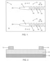
FIG. 1 is a top view of a structure at an initial fabrication stage of a processing method in accordance with embodiments of the invention. -
FIG. 2 is a cross-sectional view of the structure taken generally along line 2-2 inFIG. 1 . -
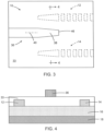
FIG. 3 is a top view of the structure at a fabrication stage subsequent toFIG. 1 . -
FIG. 4 is a cross-sectional view of the structure taken generally along line 4-4 inFIG. 3 . -
FIG. 5 is a cross-sectional view of the structure at a fabrication stage subsequent toFIG. 4 . -
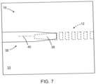
FIGS. 6-9 are top views of structures in accordance with alternative embodiments of the invention. -
FIG. 10 is a top view of a structure in accordance with alternative embodiments of the invention. -
FIG. 11 is a top view of a portion of the structure ofFIG. 10 . -
FIG. 12 is a top view of a portion of the structure ofFIG. 10 in accordance with alternative embodiments of the invention. - With reference to
FIGS. 1, 2 and in accordance with embodiments of the invention, astructure 10 for an optical reflector includes awaveguide core 12 and awaveguide core 14 that are positioned on, and above, adielectric layer 16 and asemiconductor substrate 18. In an embodiment, thedielectric layer 16 may be comprised of a dielectric material, such as silicon dioxide, and thesemiconductor substrate 18 may be comprised of a semiconductor material, such as single-crystal silicon. In an embodiment, thedielectric layer 16 may be a buried oxide layer of a silicon-on-insulator substrate, and thedielectric layer 16 may separate thewaveguide cores semiconductor substrate 18. - The
waveguide core 12 includes atapered section 20 andmultiple segments 24 that are positioned with a spaced-apart arrangement along alongitudinal axis 22. Adjacent pairs of thesegments 24 are separated in the spaced-apart arrangement by spaces or gaps G1. In an embodiment, the pitch and duty cycle of thesegments 24 may be uniform to define a periodic arrangement. In alternative embodiments, the pitch and/or the duty cycle of thesegments 24 may be apodized (i.e., non-uniform) to define a non-periodic arrangement. Thetapered section 20 may terminate at anend surface 26, and the width of thetapered section 20 may increase with increasing distance from theend surface 26. In an embodiment, thesegments 24 may have the same width dimension in a direction transverse to thelongitudinal axis 22. - The
waveguide core 14 includes atapered section 30 andmultiple segments 34 that are positioned with a spaced-apart arrangement along alongitudinal axis 32. Adjacent pairs of thesegments 34 are separated in the spaced-apart arrangement by spaces or gaps G2. In an embodiment, the pitch and duty cycle of thesegments 34 may be uniform to define a periodic arrangement. In alternative embodiments, the pitch and/or the duty cycle of thesegments 34 may be apodized (i.e., non-uniform) to define a non-periodic arrangement. The taperedsection 30 may terminate at anend surface 28, and the width of the taperedsection 30 may increase with increasing distance from theend surface 28. In an embodiment, thesegments 34 may have the same width dimension in a direction transverse to thelongitudinal axis 32. - In an embodiment, the
segments 24 and thesegments 34 may be characterized by the same pitch and/or duty cycle. In an embodiment, thesegments 24 may have a different pitch and/or duty cycle than thesegments 34. In an embodiment, thesegments 24 and thesegments 34 may have a pitch in a range of 100 nm to 1000 nm, and a duty cycle in a range of 0.2 to 0.8. - In an embodiment, the
waveguide cores waveguide cores waveguide cores waveguide cores - The
waveguide cores waveguide cores waveguide cores waveguide core 12 and/or a lower portion of thewaveguide core 14. The slab layer may be formed when thewaveguide cores dielectric layer 16, may have a thickness that is less than the thickness of thewaveguide cores - With reference to
FIGS. 3, 4 in which like reference numerals refer to like features inFIGS. 1, 2 and at a subsequent fabrication stage, adielectric layer 33 is formed over thewaveguide cores waveguide cores dielectric layer 33, which may be deposited and planarized after deposition, because thedielectric layer 33 is thicker than the height of thewaveguide cores dielectric layer 33 may be comprised of a dielectric material, such as silicon dioxide, having a refractive index that is less than the refractive index of the material constituting thewaveguide cores dielectric layer 33 may be disposed in the gaps G1 between thesegments 24 of thewaveguide core 12 and the gaps G2 between thesegments 34 of thewaveguide core 14. - A
waveguide core 36 may be formed on, and above, thedielectric layer 33. Thewaveguide core 36 may include a taperedsection 38 that is positioned in a lateral direction between thetapered section 20 of thewaveguide core 12 and the taperedsection 30 of thewaveguide core 14. Thewaveguide core 36 may extend along alongitudinal axis 40, which may be aligned parallel to thelongitudinal axis 22 of thewaveguide core 12 and thelongitudinal axis 32 of thewaveguide core 12. The taperedsection 38 may terminate at anend surface 46, and the width of the taperedsection 38 may increase with increasing distance from theend surface 46. - The tapered
section 38 of thewaveguide core 36, which is positioned adjacent to the taperedsection 20 of thewaveguide core 12 and the taperedsection 30 of thewaveguide core 14, may be longitudinally offset from thesegments 24 of thewaveguide core 12 and thesegments 34 of thewaveguide core 14. In that regard, theend surface 46 may terminate the taperedsection 38 adjacent to the taperedsections section 38 does not extend longitudinally into the space laterally between thesegments 24 and thesegments 34. The longitudinal offset restricts lateral light transfer between thesegments 24 and the taperedsection 38, as well as restricts lateral light transfer between thesegments 34 and the taperedsection 38. - The tapered
section 38 of thewaveguide core 36 is laterally offset from the taperedsection 20 andsegments 24 of thewaveguide core 12, and the taperedsection 38 of thewaveguide core 36 is laterally offset from the taperedsection 30 andsegments 34 of thewaveguide core 14. In an embodiment, the taperedsection 38 of thewaveguide core 36 may be symmetrically positioned between thetapered section 20 of thewaveguide core 12 and the taperedsection 30 of thewaveguide core 14. In an embodiment, the taperedsection 38 of thewaveguide core 36 may be asymmetrically positioned between thetapered section 20 of thewaveguide core 12 and the taperedsection 30 of thewaveguide core 14. Thewaveguide cores dielectric layer 33 such that thedielectric layer 33 separates thewaveguide core 36 from thewaveguide cores section 38 of thewaveguide core 36 has a non-overlapping relationship with the taperedsection 20 andsegments 24 of thewaveguide core 12 and with the taperedsection 30 andsegments 34 of thewaveguide core 14. - The
waveguide core 36 may be comprised of a dielectric material having a refractive index that is greater than the refractive index of silicon dioxide. In an embodiment, thewaveguide core 36 may be comprised of silicon nitride. In an embodiment, thewaveguide core 36 may be comprised of aluminum nitride or silicon oxynitride. In an embodiment,waveguide core 36 may be formed by depositing a layer of its constituent material over thedielectric layer 33 and patterning the deposited layer with lithography and etching processes. - With reference to
FIG. 5 in which like reference numerals refer to like features inFIG. 4 and at a subsequent fabrication stage, adielectric layer 42 is formed on, and above, thewaveguide core 36 anddielectric layer 33. Thedielectric layer 42 may be comprised of a dielectric material, such as silicon dioxide, having a refractive index that is less than the refractive index of the material constituting thewaveguide core 36. Thewaveguide core 36 is embedded in thedielectric layer 42, which may be deposited and planarized after deposition, because thedielectric layer 42 is thicker than the height of thewaveguide core 36. - A back-end-of-
line stack 44 may be formed over thedielectric layer 42. The back-end-of-line stack 44 may include dielectric layers that are comprised of a dielectric material, such as silicon dioxide, silicon nitride, tetraethylorthosilicate silicon dioxide, or fluorinated-tetraethylorthosilicate silicon dioxide. - In use, light may be guided on a photonics chip by the
waveguide core 36 for input to thestructure 10. The arriving light is transferred in a lateral direction from the taperedsection 38 of thewaveguide core 36 to the taperedsection 20 of thewaveguide core 12 and the taperedsection 30 of thewaveguide core 14. The transferred light propagating in thewaveguide core 12 is reflected by thesegments 24, and the transferred light propagating in thewaveguide core 14 is reflected by thesegments 34. The reflected light is transferred in a lateral direction from the taperedsection 20 of thewaveguide core 12 to the taperedsection 38 of thewaveguide core 36 and in a lateral direction from the taperedsection 30 of thewaveguide core 14 to the taperedsection 38 of thewaveguide core 36. The transferred reflected light propagates in thewaveguide core 36 out of thestructure 10. Thetapered sections structure 10 in an opposite direction from its arrival. - The
waveguide core 12 and thewaveguide core 14 define Bragg reflectors that are embedded within the optical coupler, and thesegments 24 of thewaveguide core 12 and thesegments 34 of thewaveguide core 14 define respective Bragg gratings of the Bragg reflectors. The placement of thesegments 24 of thewaveguide core 12 and thesegments 34 of thewaveguide core 14 in a different level of the optical reflector from thewaveguide core 36 permits thesegments dielectric layer 42. The dielectric material in the gaps G1 between thesegments 24 may be free of voids that would otherwise result from tighter spacing of thesegments 24, and the dielectric material in the gaps G2 between thesegments 34 may be free of voids that would otherwise result from tighter spacing of thesegments 34. The optical reflector embodied in thestructure 10 may result in improvements in performance of the optical reflector and may reduce variabilities in performance among different instances of thestructure 10. Thestructure 10 may also be deployed in other types of optical components, such as Echelle gratings and Bragg filters, that incorporate optical reflectors. - With reference to
FIG. 6 and in accordance with alternative embodiments, thewaveguide core 36 may have an overlapping relationship with the taperedsection 20 andsegments 24 of thewaveguide core 12, thewaveguide core 14 may be omitted from thestructure 10, thewaveguide core 36 may extend over and past thewaveguide core 12 without terminating at an end surface of a tapered section. A portion of thewaveguide core 36 is positioned adjacent to the taperedsection 20 andsegments 24 of thewaveguide core 12. In an embodiment, a portion of the light propagating in thewaveguide core 36 may be transferred to the taperedsection 20 and reflected by thesegments 24 back to thewaveguide core 36 for propagation in a reverse direction, and another portion of the light may continue to propagate in thewaveguide core 12 without transfer and reflection past the taperedsection 20 andsegments 24 of thewaveguide core 12. - With reference to
FIG. 7 and in accordance with alternative embodiments, the taperedsection 38 of thewaveguide core 36 may have an overlapping relationship with the taperedsection 20 of thewaveguide core 12, and thewaveguide core 14 may be omitted from thestructure 10. In use, light may be transferred in a vertical direction from the taperedsection 38 of thewaveguide core 36 to the taperedsection 20 of thewaveguide core 12, reflected by thesegments 24, and transferred from the taperedsection 20 back to the taperedsection 38 of thewaveguide core 36. - With reference to
FIG. 8 in which like reference numerals refer to like features inFIG. 7 and in accordance with alternative embodiments, awaveguide core 48 that includes a taperedsection 50 and spaced-apartsegments 54 may be formed on thedielectric layer 42 over thewaveguide core 36. Thewaveguide core 36 is positioned in a vertical direction between thewaveguide core 12 and thewaveguide core 48. The taperedsection 50 andsegments 54 may be arranged along alongitudinal axis 52, and the taperedsection 50 may have an overlapping relationship with the taperedsection 38 of thewaveguide core 36 and with the underlying taperedsection 20 of thewaveguide core 12. - In an embodiment, the
waveguide core 48 may be comprised of a material having a refractive index that is greater than the refractive index of silicon dioxide. In an embodiment, thewaveguide core 48 may be comprised of a semiconductor material, such as polysilicon or amorphous silicon, that is deposited and patterned by lithography and etching processes. The taperedsection 50 andsegments 54 may has an overlapping relationship with thewaveguide core 36. The addition of thewaveguide core 48 may enhance the light reflection in excess of the light reflection provided by thewaveguide core 12. - In an alternative embodiment, the
waveguide core 12 may be omitted from thestructure 10 such that only thewaveguide core 48 provides the light reflection. - With reference to
FIG. 9 in which like reference numerals refer to like features inFIG. 3 and in accordance with alternative embodiments, awaveguide core 58 may be formed that is laterally offset relative to thewaveguide core 36, and awaveguide core 68 may be formed that is laterally offset relative to thewaveguide core 36. Thewaveguide core 58 may have an overlapping relationship with thewaveguide core 12, and thewaveguide core 68 may have an overlapping relationship with thewaveguide core 14. Thewaveguide cores section 38 of thewaveguide core 36. - The
waveguide core 58 may include a taperedsection 60 and spaced-apartsegments 64 that are formed on thedielectric layer 42. The taperedsection 60 andsegments 64 may be arranged along alongitudinal axis 62. Thewaveguide core 68 may include a taperedsection 65 and spaced-apartsegments 66 that are formed on thedielectric layer 42. The taperedsection 65 andsegments 66 may be arranged along alongitudinal axis 67. In an embodiment, thewaveguide cores waveguide cores multiple waveguide cores waveguide cores - In an alternative embodiment, the
waveguide cores structure 10 such that only thewaveguide cores - With reference to
FIGS. 10, 11, and 12 and in accordance with alternative embodiments, astructure 70 for an Echelle grating may include multiple instances of thewaveguide core 12. Thestructure 70 includes aslab region 72, awaveguide core 74 connected to aside edge 73 of theslab region 72, andmultiple waveguide cores same side edge 73 of theslab region 72 as thewaveguide core 74. The multiple instances of thewaveguide core 12 may be deployed in a spaced-apart arrangement at acurved side edge 80 of theslab region 72 that is opposite to theside edge 73. Each instance of thewaveguide core 12 may have an overlapping relationship with thecurved side edge 80. - The different instances of the
waveguide core 12 may be tilted at different angles of inclination relative to each other, as diagrammatically shown inFIG. 10 by the different angular orientations of the dashed boxes representing the different instances of thewaveguide core 12. More specifically, thelongitudinal axes 22 of the different instances of thewaveguide core 12 may be tilted at different angles of inclination relative to each other. In an embodiment, the different instances of thewaveguide core 12 may have a width dimension W, and the width dimension that varies with increasing distance from thewaveguide core 74 such that the taperedsection 20 andsegments 24 of thewaveguide core 12 most distant from thewaveguide core 74 are characterized by the largest width dimension W and the taperedsection 20 andsegments 24 of thewaveguide core 12 closest to thewaveguide core 74 are characterized by the smallest width dimension W. - The different instances of the
waveguide core 12 define Bragg reflectors that are embedded within the Echelle grating, and thesegments 24 define Bragg gratings of the Bragg reflectors. The different instances of thewaveguide core 12 are located in a different level of thestructure 70 from theslab region 72, thewaveguide core 74, and thewaveguide cores waveguide core 12 may be disposed in a vertical direction between the semiconductor substrate 18 (FIG. 5 ) and theslab region 72,waveguide core 74, andwaveguide cores slab region 72, thewaveguide core 74, and thewaveguide cores waveguide core 12 may be comprised of a semiconductor material, such as silicon. In an embodiment and as shown inFIG. 11 , each instance of thewaveguide core 12 may include the taperedsection 20 andsegments 24. In an alternative embodiment and as shown inFIG. 12 , each instance of thewaveguide core 12 may include thesegments 24 and lack the taperedsection 20. - The Echelle grating may be deployed on a photonics chip to either multiplex or demultiplex light characterized by a broadband range, such as broadband light that spans an operating wavelength range of 1500 nm to 1600 nm. The instances of the
waveguide core 12 may demultiplex broadband light arriving via thewaveguide core 74 to provide demultiplexed light as outputs to thewaveguide cores waveguide core 12 may multiplex light arriving via thewaveguide cores waveguide core 74. The dimension of theslab region 72 between theside edge 73 and theside edge 80 promotes the multiplexing or demultiplexing by providing adequate separation space for the different optical paths of the light of different wavelengths reflected from the instances of thewaveguide core 12. - The placement of the
segments 24 of thewaveguide cores 12 in a different level from theslab region 72, thewaveguide core 74, and thewaveguide cores segments 24 to be formed with a spacing that promotes improved filling by the dielectric material of the subsequently-deposited dielectric layer 42 (FIG. 5 ). - The methods as described above are used in the fabrication of integrated circuit chips. The resulting integrated circuit chips can be distributed by the fabricator in raw wafer form (e.g., as a single wafer that has multiple unpackaged chips), as a bare die, or in a packaged form. The chip may be integrated with other chips, discrete circuit elements, and/or other signal processing devices as part of either an intermediate product or an end product. The end product can be any product that includes integrated circuit chips, such as computer products having a central processor or smartphones.
- References herein to terms modified by language of approximation, such as "about", "approximately", and "substantially", are not to be limited to the precise value specified. The language of approximation may correspond to the precision of an instrument used to measure the value and, unless otherwise dependent on the precision of the instrument, may indicate a range of +/- 10% of the stated value(s).
- References herein to terms such as "vertical", "horizontal", etc. are made by way of example, and not by way of limitation, to establish a frame of reference. The term "horizontal" as used herein is defined as a plane parallel to a conventional plane of a semiconductor substrate, regardless of its actual three-dimensional spatial orientation. The terms "vertical" and "normal" refer to a direction in the frame of reference perpendicular to the horizontal, as just defined. The term "lateral" refers to a direction in the frame of reference within the horizontal plane.
- A feature "connected" or "coupled" to or with another feature may be directly connected or coupled to or with the other feature or, instead, one or more intervening features may be present. A feature may be "directly connected" or "directly coupled" to or with another feature if intervening features are absent. A feature may be "indirectly connected" or "indirectly coupled" to or with another feature if at least one intervening feature is present. A feature "on" or "contacting" another feature may be directly on or in direct contact with the other feature or, instead, one or more intervening features may be present. A feature may be "directly on" or in "direct contact" with another feature if intervening features are absent. A feature may be "indirectly on" or in "indirect contact" with another feature if at least one intervening feature is present. Different features may "overlap" if a feature extends over, and covers a part of, another feature with either direct contact or indirect contact.
- The descriptions of the various embodiments of the present invention have been presented for purposes of illustration but are not intended to be exhaustive or limited to the embodiments disclosed. Many modifications and variations will be apparent to those of ordinary skill in the art without departing from the scope and spirit of the described embodiments. The terminology used herein was chosen to best explain the principles of the embodiments, the practical application or technical improvement over technologies found in the marketplace, or to enable others of ordinary skill in the art to understand the embodiments disclosed herein.
Claims (15)
- A structure for an optical reflector, the structure comprising:a semiconductor substrate;a first waveguide core positioned in a vertical direction over the semiconductor substrate, the first waveguide core including a first tapered section and a first plurality of segments separated by a first plurality of gaps; anda second waveguide core positioned in the vertical direction relative to the first waveguide core, the second waveguide core including a portion positioned adjacent to the first waveguide core.
- The structure of claim 1 further comprising:
a third waveguide core positioned in the vertical direction over the semiconductor substrate and adjacent to the portion of the second waveguide core, the third waveguide core including a second tapered section and a second plurality of segments separated by a second plurality of gaps. - The structure of claim 2 wherein the portion of the second waveguide core is positioned in a lateral direction between the first waveguide core and the third waveguide core.
- The structure of claim 3 wherein the first waveguide core and the third waveguide core comprise polysilicon, amorphous silicon, or single-crystal silicon, and the second waveguide core comprises silicon nitride.
- The structure of claim 2 wherein the portion of the second waveguide core is positioned in the vertical direction between the first waveguide core and the third waveguide core, and, optionally, wherein the first waveguide core comprises single-crystal silicon, the second waveguide core comprises silicon nitride, and the third waveguide core comprises polysilicon or amorphous silicon.
- The structure of claim 1 or claim 2 wherein the first waveguide core comprises single-crystal silicon, and the second waveguide core comprises silicon nitride, or wherein the first waveguide core comprises polysilicon or amorphous silicon, and the second waveguide core comprises silicon nitride.
- The structure of one of claims 1, 2, 5 and 6 wherein the second waveguide core is positioned in an overlapping arrangement with the first tapered section and the first plurality of segments of the first waveguide core.
- The structure of one of claims 1 to 6 wherein the second waveguide core includes an end and a tapered section that terminates at the end, and the first tapered section of the first waveguide core is positioned adjacent to the tapered section of the second waveguide core, and, optionally, wherein the tapered section of the second waveguide core is longitudinally offset from the first plurality of segments of the first waveguide core.
- The structure of one of claims 1 to 8 further comprising:
a dielectric layer over the first waveguide core, the dielectric layer comprising a dielectric material, and the dielectric material of the dielectric layer disposed in the first plurality of gaps of the first waveguide core. - The structure of one of claims 1 to 9 wherein the first tapered section of the first waveguide core is configured to receive light transferred from the second waveguide core, and the first plurality of segments of the first waveguide core are configured to reflect the light back to the first tapered section of the first waveguide core for transfer to the second waveguide core.
- A structure for an Echelle grating, the structure comprising:a semiconductor substrate;a slab region positioned in a vertical direction over the semiconductor substrate, the slab region include a first side edge that is curved;a first waveguide core connected to the slab region;a plurality of second waveguide cores connected to the slab region; anda plurality of Bragg reflectors positioned in the vertical direction between the slab region and the semiconductor substrate, each Bragg reflector having an overlapping relationship with the first side edge of the slab region, and each Bragg reflector including a plurality of segments separated by a plurality of gaps.
- The structure of claim 11 wherein the slab region includes a second side edge opposite to the first side edge, and the first waveguide core and the plurality of second waveguide cores are connected to the second side edge of the slab region.
- The structure of claim 11 or claim 12 wherein the plurality of Bragg reflectors are tilted at different angles of inclination relative to each other, and/or wherein each Bragg reflector includes a tapered section positioned adjacent to the plurality of segments, and/or wherein the first waveguide core, the plurality of second waveguide cores, and the slab region comprise silicon nitride, and the plurality of Bragg reflectors comprise silicon.
- The structure of one of claims 11 to 13 wherein the first waveguide core is configured to input light to the slab region, and the plurality of Bragg reflectors are configured to reflect the light toward the plurality of second waveguide cores for output from the slab region.
- A method of forming a structure for an optical reflector, the method comprising:forming a first waveguide core positioned in a vertical direction over a semiconductor substrate, wherein the first waveguide core includes a tapered section and a plurality of segments separated by a plurality of gaps; andforming a second waveguide core positioned in the vertical direction relative to the first waveguide core, wherein the second waveguide core includes a portion positioned adjacent to the first waveguide core.
Applications Claiming Priority (1)
| Application Number | Priority Date | Filing Date | Title |
|---|---|---|---|
| US18/073,144 US12276835B2 (en) | 2022-12-01 | 2022-12-01 | Optical components with one or more embedded Bragg reflectors and tapered waveguide cores |
Publications (1)
| Publication Number | Publication Date |
|---|---|
| EP4400880A1 true EP4400880A1 (en) | 2024-07-17 |
Family
ID=88416958
Family Applications (1)
| Application Number | Title | Priority Date | Filing Date |
|---|---|---|---|
| EP23204229.1A Pending EP4400880A1 (en) | 2022-12-01 | 2023-10-18 | Optical components with one or more embedded bragg reflectors |
Country Status (3)
| Country | Link |
|---|---|
| US (2) | US12276835B2 (en) |
| EP (1) | EP4400880A1 (en) |
| CN (1) | CN118131395A (en) |
Families Citing this family (1)
| Publication number | Priority date | Publication date | Assignee | Title |
|---|---|---|---|---|
| US12276835B2 (en) * | 2022-12-01 | 2025-04-15 | Globalfoundries U.S. Inc. | Optical components with one or more embedded Bragg reflectors and tapered waveguide cores |
Citations (10)
| Publication number | Priority date | Publication date | Assignee | Title |
|---|---|---|---|---|
| US6892004B1 (en) * | 2002-01-21 | 2005-05-10 | Guomin Yu | Optical coupling arrangement having low coupling loss and high production yield |
| US7151635B2 (en) * | 2004-03-24 | 2006-12-19 | Enablence, Inc. | Planar waveguide reflective diffraction grating |
| US8126300B2 (en) * | 2008-06-17 | 2012-02-28 | Enablence Inc. | Segmented waveguide structure |
| US20140233881A1 (en) * | 2013-02-15 | 2014-08-21 | Nec Corporation | Optical waveguide, optical interposer and light source |
| US10197731B2 (en) * | 2016-09-02 | 2019-02-05 | Purdue Research Foundation | Optical coupler |
| US10444434B2 (en) * | 2016-11-01 | 2019-10-15 | Purdue Research Foundation | Optical coupler having segmented waveguides for coupling electromagnetic field |
| US20210018690A1 (en) * | 2019-07-18 | 2021-01-21 | Globalfoundries Inc. | Grating couplers with a silicide mirror |
| US20220146748A1 (en) * | 2020-11-10 | 2022-05-12 | Globalfoundries U.S. Inc. | Waveguide crossings including a segmented waveguide section |
| US20220221650A1 (en) * | 2021-01-12 | 2022-07-14 | Globalfoundries U.S. Inc. | Optical components in the back-end-of-line stack of a photonics chip using plural cores vertically stacked |
| US11467343B2 (en) * | 2019-12-23 | 2022-10-11 | Globalfoundries U.S. Inc. | Optical fiber coupler having hybrid tapered waveguide segments and metamaterial segments |
Family Cites Families (23)
| Publication number | Priority date | Publication date | Assignee | Title |
|---|---|---|---|---|
| JP2004271803A (en) * | 2003-03-07 | 2004-09-30 | Hitachi Ltd | Optical waveguide device and optical system using the same |
| US20080193079A1 (en) * | 2007-02-13 | 2008-08-14 | National Research Council Of Canada | Interface Device For Performing Mode Transformation in Optical Waveguides |
| US7680371B2 (en) * | 2007-02-13 | 2010-03-16 | National Research Council Of Canada | Interface device for performing mode transformation in optical waveguides |
| US8213751B1 (en) * | 2008-11-26 | 2012-07-03 | Optonet Inc. | Electronic-integration compatible photonic integrated circuit and method for fabricating electronic-integration compatible photonic integrated circuit |
| JP6987529B2 (en) * | 2017-05-15 | 2022-01-05 | ソニーセミコンダクタソリューションズ株式会社 | Image sensor, manufacturing method of image sensor, electronic equipment, and image sensor |
| US10746925B2 (en) | 2018-01-23 | 2020-08-18 | Globalfoundries Inc. | Silicon nitride grating couplers |
| US10429582B1 (en) | 2018-05-02 | 2019-10-01 | Globalfoundries Inc. | Waveguide-to-waveguide couplers with multiple tapers |
| US10795082B1 (en) | 2019-08-14 | 2020-10-06 | Globalfoundries Inc. | Bragg gratings with airgap cladding |
| US10969544B1 (en) * | 2019-11-13 | 2021-04-06 | Globalfoundries U.S. Inc. | Grating-based filters for photonics applications |
| US11125944B2 (en) | 2020-01-14 | 2021-09-21 | Globalfoundries U.S. Inc. | Polarizer with multiple evanescently coupled waveguides |
| US11340403B2 (en) | 2020-03-03 | 2022-05-24 | Globalfoundries U.S. Inc. | Photonic component with distributed Bragg reflectors |
| US11243350B2 (en) | 2020-03-12 | 2022-02-08 | Globalfoundries U.S. Inc. | Photonic devices integrated with reflectors |
| US11029465B1 (en) | 2020-03-27 | 2021-06-08 | Globalfoundries U.S. Inc. | Micro-ring modulator |
| US11187852B1 (en) | 2021-01-28 | 2021-11-30 | Globalfoundries U.S. Inc. | Bragg gratings with silicide-coated segments |
| US11531164B2 (en) | 2021-02-08 | 2022-12-20 | Globalfoundries U.S. Inc. | Hybrid edge couplers with layers in multiple levels |
| US11703641B2 (en) * | 2021-10-26 | 2023-07-18 | Globalfoundries U.S. Inc. | Wavelength division multiplexing filters including a subwavelength grating |
| US11803010B2 (en) * | 2021-11-11 | 2023-10-31 | Globalfoundries U.S. Inc. | Optical couplers with diagonal light transfer |
| US12147075B2 (en) * | 2022-05-11 | 2024-11-19 | Globalfoundries U.S. Inc. | Back-end-of-line edge couplers with a tapered grating |
| US11782208B1 (en) * | 2022-07-06 | 2023-10-10 | Globalfoundries U.S. Inc. | Wavelength-division-multiplexing filter stages with segmented wavelength splitters |
| US12660350B2 (en) * | 2022-09-15 | 2026-06-16 | Taiwan Semiconductor Manufacturing Company Ltd. | Image sensor structure and method for forming the same |
| US12271030B2 (en) * | 2022-09-26 | 2025-04-08 | Globalfoundries U.S. Inc. | Optical couplers for transitioning between a single-layer waveguide and a multiple-layer waveguide |
| US12210135B2 (en) * | 2022-11-21 | 2025-01-28 | Globalfoundries U.S. Inc. | Optical components with an adjacent metamaterial structure |
| US12276835B2 (en) * | 2022-12-01 | 2025-04-15 | Globalfoundries U.S. Inc. | Optical components with one or more embedded Bragg reflectors and tapered waveguide cores |
-
2022
- 2022-12-01 US US18/073,144 patent/US12276835B2/en active Active
-
2023
- 2023-10-18 EP EP23204229.1A patent/EP4400880A1/en active Pending
- 2023-10-27 CN CN202311405475.4A patent/CN118131395A/en active Pending
-
2025
- 2025-03-12 US US19/077,128 patent/US20250208345A1/en active Pending
Patent Citations (10)
| Publication number | Priority date | Publication date | Assignee | Title |
|---|---|---|---|---|
| US6892004B1 (en) * | 2002-01-21 | 2005-05-10 | Guomin Yu | Optical coupling arrangement having low coupling loss and high production yield |
| US7151635B2 (en) * | 2004-03-24 | 2006-12-19 | Enablence, Inc. | Planar waveguide reflective diffraction grating |
| US8126300B2 (en) * | 2008-06-17 | 2012-02-28 | Enablence Inc. | Segmented waveguide structure |
| US20140233881A1 (en) * | 2013-02-15 | 2014-08-21 | Nec Corporation | Optical waveguide, optical interposer and light source |
| US10197731B2 (en) * | 2016-09-02 | 2019-02-05 | Purdue Research Foundation | Optical coupler |
| US10444434B2 (en) * | 2016-11-01 | 2019-10-15 | Purdue Research Foundation | Optical coupler having segmented waveguides for coupling electromagnetic field |
| US20210018690A1 (en) * | 2019-07-18 | 2021-01-21 | Globalfoundries Inc. | Grating couplers with a silicide mirror |
| US11467343B2 (en) * | 2019-12-23 | 2022-10-11 | Globalfoundries U.S. Inc. | Optical fiber coupler having hybrid tapered waveguide segments and metamaterial segments |
| US20220146748A1 (en) * | 2020-11-10 | 2022-05-12 | Globalfoundries U.S. Inc. | Waveguide crossings including a segmented waveguide section |
| US20220221650A1 (en) * | 2021-01-12 | 2022-07-14 | Globalfoundries U.S. Inc. | Optical components in the back-end-of-line stack of a photonics chip using plural cores vertically stacked |
Also Published As
| Publication number | Publication date |
|---|---|
| CN118131395A (en) | 2024-06-04 |
| US20250208345A1 (en) | 2025-06-26 |
| US12276835B2 (en) | 2025-04-15 |
| US20240184042A1 (en) | 2024-06-06 |
Similar Documents
| Publication | Publication Date | Title |
|---|---|---|
| US11378743B1 (en) | Optical components in the back-end-of-line stack of a photonics chip using plural cores vertically stacked | |
| US11662523B2 (en) | Edge couplers in the back-end-of-line stack of a photonics chip | |
| US11467341B2 (en) | Waveguide crossings including a segmented waveguide section | |
| US12147075B2 (en) | Back-end-of-line edge couplers with a tapered grating | |
| US10795082B1 (en) | Bragg gratings with airgap cladding | |
| KR102877953B1 (en) | Edge couplers with consecutively-arranged tapers | |
| US11493686B2 (en) | Optical components with power-handling assistance | |
| US20250208345A1 (en) | Optical components with one or more embedded bragg reflectors | |
| KR20140039584A (en) | The optical filter having total reflection echelle grating by single reflecting and the waveguide device having the same | |
| US11782208B1 (en) | Wavelength-division-multiplexing filter stages with segmented wavelength splitters | |
| EP4400883B1 (en) | Directional couplers with heterogenous claddings | |
| EP4343394A1 (en) | Optical couplers for transitioning between a single-layer waveguide and a multiple-layer waveguide | |
| KR102891313B1 (en) | Edge couplers including a metamaterial layer | |
| US11703641B2 (en) | Wavelength division multiplexing filters including a subwavelength grating | |
| US10816872B1 (en) | Tunable grating couplers | |
| US11803010B2 (en) | Optical couplers with diagonal light transfer | |
| US10969544B1 (en) | Grating-based filters for photonics applications | |
| EP4372426A1 (en) | Optical components with an adjacent metamaterial structure | |
| EP4220257B1 (en) | Multiple-core heterogeneous waveguide structures including multiple slots | |
| EP4310561B1 (en) | SHAFT CONDUCTOR INTERSECTIONS WITH A NON-CONTACT MULTI-LEVEL ARRANGEMENT | |
| US12204146B2 (en) | Waveguide crossings with a free space propagation region | |
| EP4686965A1 (en) | Multiple-width delay arms for a wavelength-division-multiplexing filter | |
| US20260050123A1 (en) | Mach-zehnder interferometers with phase delay arms having a metamaterial region | |
| US20250264659A1 (en) | Photonic chips including a structure enabling measurement of the group velocity of light in a photonic component |
Legal Events
| Date | Code | Title | Description |
|---|---|---|---|
| PUAI | Public reference made under article 153(3) epc to a published international application that has entered the european phase |
Free format text: ORIGINAL CODE: 0009012 |
|
| STAA | Information on the status of an ep patent application or granted ep patent |
Free format text: STATUS: THE APPLICATION HAS BEEN PUBLISHED |
|
| AK | Designated contracting states |
Kind code of ref document: A1 Designated state(s): AL AT BE BG CH CY CZ DE DK EE ES FI FR GB GR HR HU IE IS IT LI LT LU LV MC ME MK MT NL NO PL PT RO RS SE SI SK SM TR |
|
| STAA | Information on the status of an ep patent application or granted ep patent |
Free format text: STATUS: REQUEST FOR EXAMINATION WAS MADE |
|
| 17P | Request for examination filed |
Effective date: 20241122 |
|
| RBV | Designated contracting states (corrected) |
Designated state(s): AL AT BE BG CH CY CZ DE DK EE ES FI FR GB GR HR HU IE IS IT LI LT LU LV MC ME MK MT NL NO PL PT RO RS SE SI SK SM TR |
|
| STAA | Information on the status of an ep patent application or granted ep patent |
Free format text: STATUS: EXAMINATION IS IN PROGRESS |
|
| 17Q | First examination report despatched |
Effective date: 20251121 |