EP4398562B1 - Image-forming apparatus and controller - Google Patents
Image-forming apparatus and controller Download PDFInfo
- Publication number
- EP4398562B1 EP4398562B1 EP23220207.7A EP23220207A EP4398562B1 EP 4398562 B1 EP4398562 B1 EP 4398562B1 EP 23220207 A EP23220207 A EP 23220207A EP 4398562 B1 EP4398562 B1 EP 4398562B1
- Authority
- EP
- European Patent Office
- Prior art keywords
- light
- emitting time
- scanning
- image
- time period
- Prior art date
- Legal status (The legal status is an assumption and is not a legal conclusion. Google has not performed a legal analysis and makes no representation as to the accuracy of the status listed.)
- Active
Links
Images




Classifications
-
- H—ELECTRICITY
- H04—ELECTRIC COMMUNICATION TECHNIQUE
- H04N—PICTORIAL COMMUNICATION, e.g. TELEVISION
- H04N1/00—Scanning, transmission or reproduction of documents or the like, e.g. facsimile transmission; Details thereof
- H04N1/04—Scanning arrangements, i.e. arrangements for the displacement of active reading or reproducing elements relative to the original or reproducing medium, or vice versa
- H04N1/047—Detection, control or error compensation of scanning velocity or position
- H04N1/0476—Indicating the scanning velocity
-
- B—PERFORMING OPERATIONS; TRANSPORTING
- B41—PRINTING; LINING MACHINES; TYPEWRITERS; STAMPS
- B41J—TYPEWRITERS; SELECTIVE PRINTING MECHANISMS, i.e. MECHANISMS PRINTING OTHERWISE THAN FROM A FORME; CORRECTION OF TYPOGRAPHICAL ERRORS
- B41J2/00—Typewriters or selective printing mechanisms characterised by the printing or marking process for which they are designed
- B41J2/435—Typewriters or selective printing mechanisms characterised by the printing or marking process for which they are designed characterised by selective application of radiation to a printing material or impression-transfer material
- B41J2/47—Typewriters or selective printing mechanisms characterised by the printing or marking process for which they are designed characterised by selective application of radiation to a printing material or impression-transfer material using the combination of scanning and modulation of light
- B41J2/471—Typewriters or selective printing mechanisms characterised by the printing or marking process for which they are designed characterised by selective application of radiation to a printing material or impression-transfer material using the combination of scanning and modulation of light using dot sequential main scanning by means of a light deflector, e.g. a rotating polygonal mirror
-
- G—PHYSICS
- G03—PHOTOGRAPHY; CINEMATOGRAPHY; ANALOGOUS TECHNIQUES USING WAVES OTHER THAN OPTICAL WAVES; ELECTROGRAPHY; HOLOGRAPHY
- G03G—ELECTROGRAPHY; ELECTROPHOTOGRAPHY; MAGNETOGRAPHY
- G03G15/00—Apparatus for electrographic processes using a charge pattern
- G03G15/04—Apparatus for electrographic processes using a charge pattern for exposing, i.e. imagewise exposure by optically projecting the original image on a photoconductive recording material
- G03G15/043—Apparatus for electrographic processes using a charge pattern for exposing, i.e. imagewise exposure by optically projecting the original image on a photoconductive recording material with means for controlling illumination or exposure
-
- G—PHYSICS
- G03—PHOTOGRAPHY; CINEMATOGRAPHY; ANALOGOUS TECHNIQUES USING WAVES OTHER THAN OPTICAL WAVES; ELECTROGRAPHY; HOLOGRAPHY
- G03G—ELECTROGRAPHY; ELECTROPHOTOGRAPHY; MAGNETOGRAPHY
- G03G15/00—Apparatus for electrographic processes using a charge pattern
- G03G15/50—Machine control of apparatus for electrographic processes using a charge pattern, e.g. regulating differents parts of the machine, multimode copiers, microprocessor control
-
- G—PHYSICS
- G06—COMPUTING OR CALCULATING; COUNTING
- G06K—GRAPHICAL DATA READING; PRESENTATION OF DATA; RECORD CARRIERS; HANDLING RECORD CARRIERS
- G06K15/00—Arrangements for producing a permanent visual presentation of the output data, e.g. computer output printers
- G06K15/02—Arrangements for producing a permanent visual presentation of the output data, e.g. computer output printers using printers
- G06K15/12—Arrangements for producing a permanent visual presentation of the output data, e.g. computer output printers using printers by photographic printing, e.g. by laser printers
- G06K15/1204—Arrangements for producing a permanent visual presentation of the output data, e.g. computer output printers using printers by photographic printing, e.g. by laser printers involving the fast moving of an optical beam in the main scanning direction
-
- H—ELECTRICITY
- H04—ELECTRIC COMMUNICATION TECHNIQUE
- H04N—PICTORIAL COMMUNICATION, e.g. TELEVISION
- H04N2201/00—Indexing scheme relating to scanning, transmission or reproduction of documents or the like, and to details thereof
- H04N2201/04—Scanning arrangements
- H04N2201/047—Detection, control or error compensation of scanning velocity or position
- H04N2201/04753—Control or error compensation of scanning position or velocity
- H04N2201/04758—Control or error compensation of scanning position or velocity by controlling the position of the scanned image area
- H04N2201/04767—Control or error compensation of scanning position or velocity by controlling the position of the scanned image area by controlling the timing of the signals, e.g. by controlling the frequency o phase of the pixel clock
-
- H—ELECTRICITY
- H04—ELECTRIC COMMUNICATION TECHNIQUE
- H04N—PICTORIAL COMMUNICATION, e.g. TELEVISION
- H04N2201/00—Indexing scheme relating to scanning, transmission or reproduction of documents or the like, and to details thereof
- H04N2201/04—Scanning arrangements
- H04N2201/047—Detection, control or error compensation of scanning velocity or position
- H04N2201/04753—Control or error compensation of scanning position or velocity
- H04N2201/04758—Control or error compensation of scanning position or velocity by controlling the position of the scanned image area
- H04N2201/04767—Control or error compensation of scanning position or velocity by controlling the position of the scanned image area by controlling the timing of the signals, e.g. by controlling the frequency o phase of the pixel clock
- H04N2201/04768—Controlling the frequency of the signals
-
- H—ELECTRICITY
- H04—ELECTRIC COMMUNICATION TECHNIQUE
- H04N—PICTORIAL COMMUNICATION, e.g. TELEVISION
- H04N2201/00—Indexing scheme relating to scanning, transmission or reproduction of documents or the like, and to details thereof
- H04N2201/04—Scanning arrangements
- H04N2201/047—Detection, control or error compensation of scanning velocity or position
- H04N2201/04753—Control or error compensation of scanning position or velocity
- H04N2201/04789—Control or error compensation of scanning position or velocity in the main-scan direction
-
- H—ELECTRICITY
- H04—ELECTRIC COMMUNICATION TECHNIQUE
- H04N—PICTORIAL COMMUNICATION, e.g. TELEVISION
- H04N2201/00—Indexing scheme relating to scanning, transmission or reproduction of documents or the like, and to details thereof
- H04N2201/04—Scanning arrangements
- H04N2201/047—Detection, control or error compensation of scanning velocity or position
- H04N2201/04753—Control or error compensation of scanning position or velocity
- H04N2201/04793—Control or error compensation of scanning position or velocity using stored control or compensation data, e.g. previously measured data
-
- H—ELECTRICITY
- H04—ELECTRIC COMMUNICATION TECHNIQUE
- H04N—PICTORIAL COMMUNICATION, e.g. TELEVISION
- H04N2201/00—Indexing scheme relating to scanning, transmission or reproduction of documents or the like, and to details thereof
- H04N2201/04—Scanning arrangements
- H04N2201/047—Detection, control or error compensation of scanning velocity or position
- H04N2201/04753—Control or error compensation of scanning position or velocity
- H04N2201/04794—Varying the control or compensation during the scan, e.g. using continuous feedback or from line to line
-
- H—ELECTRICITY
- H04—ELECTRIC COMMUNICATION TECHNIQUE
- H04N—PICTORIAL COMMUNICATION, e.g. TELEVISION
- H04N2201/00—Indexing scheme relating to scanning, transmission or reproduction of documents or the like, and to details thereof
- H04N2201/04—Scanning arrangements
- H04N2201/047—Detection, control or error compensation of scanning velocity or position
- H04N2201/04753—Control or error compensation of scanning position or velocity
- H04N2201/04794—Varying the control or compensation during the scan, e.g. using continuous feedback or from line to line
- H04N2201/04798—Varying the main-scan control during the main-scan, e.g. facet tracking
Definitions
- the present disclosure generally relates to the field of optical scanning technology and, more particularly, relates to an image-forming apparatus and a controller.
- a laser printer typically includes an optical scanning unit for exposing a photosensitive member.
- the optical scanning unit emits laser based on image data.
- the laser is reflected by a rotating polygon mirror, and reflected laser light is then transmitted through a scanning lens. Transmitted light irradiates a photosensitive drum to expose the photosensitive drum.
- a laser spot formed on the surface of the photosensitive drum continuously moves to achieve scanning, thereby forming a latent image on the photosensitive member.
- An existing scanning lens may have F- ⁇ characteristics.
- the lens with F- ⁇ characteristics may cause the laser spot to move on the surface of the photosensitive member at a uniform linear velocity when the polygon mirror rotates at a uniform angular velocity.
- the scanning lens with F- ⁇ characteristics may be configured to perform proper exposure.
- the scanning lens with F- ⁇ characteristics may have relatively large size and high cost. Therefore, in order to reduce the size and cost of an image-forming apparatus, the scanning lens without F- ⁇ characteristics may be configured.
- Patent document US5933184 refers to an image forming apparatus performing correction of scanning deviation due to inaccuracy of the optical system.
- Patent document US2004227807 refers to an image forming apparatus performing correction of scanning deviation due to absence or over/under-correction of an F-Theta lens arrangement.
- electrical correction may be performed to change an image clock frequency during a scanning operation, such that when the laser spot does not move at a uniform speed on the surface of the photosensitive member, no pixel deviation may be in the laser spot formed on the surface of the photosensitive member.
- the exposure amounts of the pixels at an end region and a central region of the photosensitive member along a main scanning direction may also change, and such difference in exposure amounts may cause image degradation.
- the image-forming apparatus includes a photosensitive member; a scanning unit, configured to perform laser scanning on the photosensitive member at a non-constant linear speed along a main scanning direction to form an electrostatic latent image; and a controller, configured to make a scanning period T1 corresponding to a first pixel at a central region of the photosensitive member to be not equal to a scanning period T2 corresponding to a second pixel at a non-central region of the photosensitive member.
- the first pixel and the second pixel are each configured with a light-emitting time period and a non-light-emitting time period; the light-emitting time period satisfies that a light-emitting time length of the light-emitting time period of the first pixel is same as a light-emitting time length of the light-emitting time period of the second pixel; and for printing a fixed page, a light-emitting power of the scanning unit is a preset fixed value.
- the controller is configured to make T1 greater than T2 or T1 smaller than T2.
- the light-emitting time period is configured continuously or discontinuously in a scanning period.
- the light-emitting time period is at a middle section of a scanning period; and the non-light-emitting time period is at a first section and a last section of the scanning period.
- a quantity of the light-emitting time period is at least 1; and/or a quantity of the non-light-emitting time period is at least 1.
- the controller is configured to control the scanning unit to emit light or not to emit light through a video signal.
- a proportion of the light-emitting time period to a total time of the scanning period is not higher than 3/4.
- the non-central region further includes an end region and at least one transition region, wherein a scanning period of a pixel in the end region is shorter than a scanning period of a pixel in the transition region.
- the scanning unit includes a rotating polygon mirror capable of reflecting a laser, the laser reflected by the rotating polygon mirror is applied to the photosensitive member through an image-forming lens, and the image-forming lens is not capable of correcting the laser along the main scanning direction to be linear.
- a controller is configured to make a scanning period T1 corresponding to a first pixel at a central region of a photosensitive member to be not equal to a scanning period T2 corresponding to a second pixel at a non-central region of the photosensitive member, where the first pixel and the second pixel are each configured with a light-emitting time period and a non-light-emitting time period; the light-emitting time period satisfies that a light-emitting time length of the light-emitting time period of the first pixel is same as a light-emitting time length of the light-emitting time period of the second pixel; and for printing a fixed page, a light-emitting power of the scanning unit is a preset fixed value.
- FIG. 1 illustrates a schematic of a laser-type image-forming apparatus provided by exemplary embodiments of the present disclosure.
- a laser driving unit 300 included in an optical scanning device 400 as an optical scanning unit may be configured to generate scanning light (i.e., laser) 208 in response to an image signal outputted from an image signal generation unit 100 and a control signal outputted from a control unit 1.
- a photosensitive drum 4 that the surface of the photosensitive drum is charged may be scanned by the laser 208, such that a latent image may be formed on the surface of the photosensitive drum 4.
- a developing unit (not shown) may apply toner to the latent image to form a toner image corresponding to the latent image.
- the toner image may be transferred to a recording medium (such as paper), thereby completing a forming process of one image.
- a controller mentioned in the present disclosure may be a single piece including the image signal generation unit 100 and the control unit 1.
- An example of the scanning unit mentioned in the present disclosure may be the optical scanning device 400 in FIG. 1 which may function as the scanning unit.
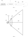
- FIG. 2 illustrates a cross-sectional view of the optical scanning device 400 along a main scanning direction.
- the main scanning direction may be a direction in parallel with the surface of the photosensitive drum 4 and orthogonal to a moving direction on the surface of the photosensitive drum 4.
- the scanning light (e.g., laser) 208 emitted from a light source 401 may be reflected by a reflective surface of a rotating polygon mirror 405 after passing through an optical lens assembly (not shown).
- the light (e.g., light beam) reflected by the reflective surface may be configured as the scanning light 208, and the scanning light 208 may irradiate onto a scanning surface 407 to form a spot image.
- the rotating polygon mirror 405 is rotated by a driving unit (not shown) at a constant angular velocity along the direction indicated by an arrow A
- the light spot may move on the scanning surface 407 along the main scanning direction, such that the electrostatic latent image may be formed on the scanning surface 407.
- the linear speed of the light spot moving along the main scanning direction may be not constant, that is, the linear speed at the end may be faster than the linear speed at the center.
- Such linear velocity inconsistency may lead to scanning deviation.
- Such deviation problem may be solved by designing an image-forming lens 406 as the lens with F- ⁇ characteristics.
- the F- ⁇ lens may achieve linear scanning with incident light of constant angular velocity.
- the lens with F- ⁇ characteristics may be relatively large and expensive and require more space inside the printer; or in some image-forming apparatuses using the F- ⁇ lens, the characteristics of the F- ⁇ lens may be not sufficient to completely correct the laser along the main scanning direction to be linear.
- the control period T2 corresponding to image pixels at the end region may be shorter than the control period T1 corresponding to image pixels at the central region.
- the control period T2 corresponding to image pixels at the end region may be shorter than the control period T1 corresponding to image pixels at the central region.
- FIG. 3 it can be seen from FIG. 3 that, due to different lengths of the control periods, when the output power of the laser remains unchanged, actual exposure amounts of all pixels at the end region and the central region may be inconsistent. Such exposure inconsistency may result in different toner densities at the end region and the central region (i.e., P1 and P2 in FIG. 3 ), which may reduce image quality.
- a technology solution of adjusting exposure amounts according to the positions may be provided; that is, the laser output power when the end region is scanned may be lower than the laser output power when the central region is scanned.
- relatively high accuracy of the control signal may be needed, and the controller may need to at least ensure that a VIDEO signal and a brightness control signal are maintained to be highly synchronized, which may increase development cost of the image-forming apparatus and increase the types of failures such as signal desynchronization.
- the image-forming apparatus may include a photosensitive member; a scanning unit, configured to scan the photosensitive member at a non-constant linear speed along the main scanning direction to form an electrostatic latent image on the photosensitive member; and a controller, configured to make the scanning period T1 corresponding to the first pixel at the central region of the photosensitive member to be not equal to the scanning period T2 corresponding to the second pixel at a non-central region of the photosensitive member.
- Both the first pixel and the second pixel may be configured with a light-emitting time period and a non-light-emitting time period; the light-emitting time period may satisfy that the light-emitting time length of the light-emitting time period of the first pixel may be same as the light-emitting time length of the light-emitting time period of the second pixel.
- the light-emitting power of the scanning unit may be a preset fixed value.
- the non-central region in the present disclosure may further include an end region and at least one transition region, where the scanning period of the pixel in the end region may be shorter than the scanning period of the pixel in the transition region.
- the photosensitive member 4 may sequentially include a left end region A1, a left sub-end region B1, a left sub-central region C1 and a central region D from the left end to the center.
- the photosensitive member may sequentially include a central region D, a right sub-central region C2, a right sub-end region B2, and a right end region A2 from the center to the right end.
- the left sub-end region B1, the left sub-central region C1, the right sub-central region C2, and the right sub-end region B2 may be regarded as transition regions. In one embodiment, it assumes that scanning may be performed from left to right along the main scanning direction.
- the scanning unit may have the following characteristics that the scanning speed of the end region on the scanning surface 407 may be higher than the scanning speed of the central region, which is because when the rotational angular velocity of the rotating polygon mirror (i.e., deflector) 405 is constant, the reflective surface may be further away from the end region of the photosensitive drum than from the central region of the photosensitive drum. Since the linear velocity is equal to the product of angular velocity and radius, it should be noted that the scanning linear velocity of the end region may be higher than the scanning linear velocity of the central region. That is, the scanning unit in one embodiment may perform laser scanning on the surface of the photosensitive member at a non-constant linear velocity.
- the image signal generation unit 100 may receive printing information from a computer and generate the VIDEO signal corresponding to image data; and the laser driving unit 300 may supply current to the light source 401 in response to the VIDEO signal to cause the light source 401 to emit light, such that the latent image corresponding to the VIDEO signal may be formed on the scanning surface.
- the image deviation problem caused by non-constant scanning speed may be solved by setting the period of the VIDEO signal. That is, the period T1 of the VIDEO signal corresponding to the pixel at the non-central region (such as the end region) may be shorter, and the period T2 of the VIDEO signal corresponding to the pixel at the central region may be longer.
- it may further configure the time of the VIDEO signal at an ON state (i.e., the laser emits light) in a period; and for remaining time of such period, the VIDEO signal may be at an OFF state (i.e., the laser does not emit light). That is, the VIDEO signal may be configured to control the scanning unit to emit light or not to emit light.
- an ON state i.e., the laser emits light
- the VIDEO signal may be at an OFF state (i.e., the laser does not emit light). That is, the VIDEO signal may be configured to control the scanning unit to emit light or not to emit light.
- the period T1 of the VIDEO signal corresponding to the pixel at the non-central region may be longer, and the period T2 of the VIDEO signal corresponding to the pixel at the central region may be shorter, which is due to "over-correction" of above-mentioned image-forming lens 406.
- the scanning speed of the end region on the scanning surface 407 may be lower than the scanning speed of the central region on the scanning surface 407.
- the controller may be configured to make that T1 is smaller than T2.
- FIG. 5A The first VIDEO signal example is shown in FIG. 5A , where SubPixel refers to the light-emitting unit time of the laser.
- FIG. 5A may correspond to one control period in the A1 and A2 regions in FIG. 4 .
- one control period may include 32 SubPixels; 24 SubPixels in the middle section of the control period may be configured to be at the ON state; and 4 SubPixels in the first section and last section of the control period may be configured to be at the OFF state.
- FIG. 5B may correspond to one control period in the B1 and B2 regions in FIG. 4 .
- one control period may include 34 SubPixels; 24 SubPixels in the middle section of the control period may be configured to be at the ON state; and 5 SubPixels in the first section and last section of the control period may be configured to be at the OFF state.
- FIG. 5C may correspond to one control period in the C1 and C2 regions in FIG. 4 .
- one control period may include 36 SubPixels; 24 SubPixels in the middle section of the control period may be configured to be at the ON state; and 6 SubPixels in the first section and last section of the control period may be configured to be at the OFF state.
- FIG. 5D may correspond to one control period in region D in FIG. 4 .
- one control period may include 40 SubPixels; 24 SubPixels in the middle section of the control period may be configured to be at the ON state; and 8 SubPixels in the first section and last section of the control period may be configured to be at the OFF state.
- SubPixel positions that the VIDEO signal is at the ON state that is, the positions that the VIDEO signal is at the ON state may be at the first section or last section of entire control period.
- the SubPixels that the VIDEO signal is at the ON state may be continuous or non-continuous.
- 24 SubPixels that the VIDEO signal is at the ON state may be continuous; or the SubPixels that the VIDEO signal is at the ON state may be configured to be spaced apart from the SubPixels that the VIDEO signal is at the ON state.
- the number of light-emitting time periods may be at least 1, and/or the number of non-light-emitting time periods may be at least 1.
- the number of light-emitting time periods may be 1, and the number of non-light-emitting time periods may be 2.
- the number of light-emitting time periods may also be configured to 2, and the number of non-light-emitting time periods may be configured to 1, which may not be limited in the present disclosure.
- FIG. 6 illustrates a schematic of one embodiment of the present disclosure.
- L3 denotes a schematic of the light-emitting time period at the central region
- L4 denotes a schematic of the light-emitting time period at the end region
- the dotted box represents the control period
- T3 denotes actual light-emitting time period in the control period. It may be seen from FIG. 6 that although the control periods at the end region and the central region are different, actual light-emitting time periods may be same. Therefore, the toner density P3 at the central region and the toner density P4 at the end regions may be same without density difference.
- the maximum value of the light-emitting time period should not exceed total time length of one scanning period at the end region, otherwise the light-emitting time periods at the end region and other regions may be not consistent with each other. If the proportion of the light-emitting time period to total time of the scanning period is no more than 3/4, the problem of inconsistent pixel widths may also be reduced.
- Pixel width refers to the product of exposure time of unit pixel and the scanning linear velocity. In the present disclosure, the light-emitting time periods in the scanning period of the pixels at the central region and the non-central region may be same, but the scanning linear velocities may be different, and theoretically the pixel widths may be different. If the proportion of the light-emitting time period to total time of the scanning period is reduced to less than 3/4, the problem of inconsistent pixel widths may be no longer obvious and the impact on image quality may be reduced.
- the scanning unit may include a rotating polygon mirror for reflecting laser.
- the laser reflected by the rotating polygon mirror may be applied to the photosensitive member through the image-forming lens, and the image-forming lens cannot correct the laser along the main scanning direction to be linear. That is, the image-forming lens used in one embodiment may have certain optical correction characteristics but may not completely correct the scanning light beam to be linear.
- above-mentioned manner for configuring the light-emitting time period and the non-light-emitting time period may also be used to solve such problem.
- the present disclosure further provides a controller, applied to the image-forming apparatus.
- the image-forming lens used in the image-forming apparatus cannot correct the laser along the main scanning direction to be linear.
- the controller may be configured to make the scanning period T1 corresponding to the first pixel at the central region of the photosensitive member to be not equal to the scanning period T2 corresponding to the second pixel at the non-central region of the photosensitive member.
- Both the first pixel and the second pixel may be configured with the light-emitting time period and the non-light-emitting time period; the light-emitting time period may satisfy that the light-emitting time length of the light-emitting time period of the first pixel may be same as the light-emitting time length of the light-emitting time period of the second pixel.
- the light-emitting power of the scanning unit may be a preset fixed value.
- the controller used in exemplary embodiment two may be applied to the image-forming apparatus without the F- ⁇ lens and may also be applied to the image-forming apparatus including an optical correction lens that the correction characteristics of the lens are not sufficient to completely correct the scanning light beam to be linear.
- the controller may include the image signal generation unit 100 and the control unit 1 as shown in FIG. 1 .
- the controller may control the scanning unit to emit light or not to emit light through the VIDEO signal. Parts of the controller in exemplary embodiment two same as those in exemplary embodiment one may not be described in detail herein.
- the technical solutions provided by the present disclosure may achieve at least the following beneficial effects.
- the exposure amounts of the pixels at different regions along the main scanning direction may be same, which may reduce the problem of inconsistent image density at different regions which easily occurs in the existing technology, thereby improving image quality.
- the control logic of the present disclosure may be simple and easy to be configured and adjusted.
Landscapes
- Physics & Mathematics (AREA)
- Engineering & Computer Science (AREA)
- General Physics & Mathematics (AREA)
- Optics & Photonics (AREA)
- General Engineering & Computer Science (AREA)
- Theoretical Computer Science (AREA)
- Microelectronics & Electronic Packaging (AREA)
- Multimedia (AREA)
- Signal Processing (AREA)
- Facsimile Scanning Arrangements (AREA)
- Mechanical Optical Scanning Systems (AREA)
- Laser Beam Printer (AREA)
Description
- The present disclosure generally relates to the field of optical scanning technology and, more particularly, relates to an image-forming apparatus and a controller.
- A laser printer typically includes an optical scanning unit for exposing a photosensitive member. The optical scanning unit emits laser based on image data. The laser is reflected by a rotating polygon mirror, and reflected laser light is then transmitted through a scanning lens. Transmitted light irradiates a photosensitive drum to expose the photosensitive drum. As the polygon mirror rotates, a laser spot formed on the surface of the photosensitive drum continuously moves to achieve scanning, thereby forming a latent image on the photosensitive member.
- An existing scanning lens may have F-θ characteristics. The lens with F-θ characteristics may cause the laser spot to move on the surface of the photosensitive member at a uniform linear velocity when the polygon mirror rotates at a uniform angular velocity. The scanning lens with F-θ characteristics may be configured to perform proper exposure.
- However, the scanning lens with F-θ characteristics may have relatively large size and high cost. Therefore, in order to reduce the size and cost of an image-forming apparatus, the scanning lens without F-θ characteristics may be configured.
- Patent document
US5933184 refers to an image forming apparatus performing correction of scanning deviation due to inaccuracy of the optical system. Patent documentUS2004227807 refers to an image forming apparatus performing correction of scanning deviation due to absence or over/under-correction of an F-Theta lens arrangement. - In the existing technology, electrical correction may be performed to change an image clock frequency during a scanning operation, such that when the laser spot does not move at a uniform speed on the surface of the photosensitive member, no pixel deviation may be in the laser spot formed on the surface of the photosensitive member.
- However, in above-mentioned existing technology, due to the change in the clock frequency, the exposure amounts of the pixels at an end region and a central region of the photosensitive member along a main scanning direction may also change, and such difference in exposure amounts may cause image degradation.
- One aspect of the present disclosure provides an image-forming apparatus. The image-forming apparatus includes a photosensitive member; a scanning unit, configured to perform laser scanning on the photosensitive member at a non-constant linear speed along a main scanning direction to form an electrostatic latent image; and a controller, configured to make a scanning period T1 corresponding to a first pixel at a central region of the photosensitive member to be not equal to a scanning period T2 corresponding to a second pixel at a non-central region of the photosensitive member. The first pixel and the second pixel are each configured with a light-emitting time period and a non-light-emitting time period; the light-emitting time period satisfies that a light-emitting time length of the light-emitting time period of the first pixel is same as a light-emitting time length of the light-emitting time period of the second pixel; and for printing a fixed page, a light-emitting power of the scanning unit is a preset fixed value.
- In an alternative embodiment, the controller is configured to make T1 greater than T2 or T1 smaller than T2.
- In an alternative embodiment, the light-emitting time period is configured continuously or discontinuously in a scanning period.
- In an alternative embodiment, the light-emitting time period is at a middle section of a scanning period; and the non-light-emitting time period is at a first section and a last section of the scanning period.
- In an alternative embodiment, a quantity of the light-emitting time period is at least 1; and/or a quantity of the non-light-emitting time period is at least 1.
- In an alternative embodiment, the controller is configured to control the scanning unit to emit light or not to emit light through a video signal.
- In an alternative embodiment, a proportion of the light-emitting time period to a total time of the scanning period is not higher than 3/4.
- In an alternative embodiment, the non-central region further includes an end region and at least one transition region, wherein a scanning period of a pixel in the end region is shorter than a scanning period of a pixel in the transition region.
- In an alternative embodiment, the scanning unit includes a rotating polygon mirror capable of reflecting a laser, the laser reflected by the rotating polygon mirror is applied to the photosensitive member through an image-forming lens, and the image-forming lens is not capable of correcting the laser along the main scanning direction to be linear.
- Another aspect of the present disclosure provides a controller, applied to an image-forming apparatus, where an image-forming lens of the image-forming apparatus is not capable of correcting a laser along a main scanning direction to be linear. A controller is configured to make a scanning period T1 corresponding to a first pixel at a central region of a photosensitive member to be not equal to a scanning period T2 corresponding to a second pixel at a non-central region of the photosensitive member, where the first pixel and the second pixel are each configured with a light-emitting time period and a non-light-emitting time period; the light-emitting time period satisfies that a light-emitting time length of the light-emitting time period of the first pixel is same as a light-emitting time length of the light-emitting time period of the second pixel; and for printing a fixed page, a light-emitting power of the scanning unit is a preset fixed value.
- Other aspects of the present disclosure may be understood by those skilled in the art in light of the description, the claims, and the drawings of the present disclosure.
- To clearly describe technical solutions of various embodiments of the present disclosure, the drawings which need to be configured for describing various embodiments are described below. Obviously, the drawings in the following description are merely some embodiments of the present disclosure. For those skilled in the art, other drawings may be obtained in accordance with the drawings without creative efforts.
-
FIG. 1 illustrates a schematic of a laser-type image-forming apparatus provided by exemplary embodiments of the present disclosure. -
FIG. 2 illustrates a cross-sectional view of an optical scanning device along a main scanning direction. -
FIG. 3 illustrates a principle schematic of a method for reducing scanning deviation. -
FIG. 4 illustrates a region schematic of a photosensitive member along a main scanning direction provided by exemplary embodiments of the present disclosure. -
FIG. 5A illustrates a schematic of a proportion of a light-emitting time period of A1 and A2 regions in a control period. -
FIG. 5B illustrates a schematic of a proportion of a light-emitting time period of B1 and B2 regions in a control period. -
FIG. 5C illustrates a schematic of a proportion of a light-emitting time period of C1 and C2 regions in a control period. -
FIG. 5D illustrates a schematic of a proportion of a light-emitting time period of a D region in a control period. -
FIG. 6 illustrates a schematic of a light-emitting time period and a toner density provided by exemplary embodiments of the present disclosure. - In order to better understand the technical solutions of the present disclosure, embodiments of the present disclosure are described in detail below with reference to accompanying drawings.
- It should be understood that described embodiments are only some of embodiments of the present disclosure, rather than all of embodiments. According to embodiments in present disclosure, all other embodiments obtained by those skilled in the art without making creative efforts should fall within the protection scope of present disclosure.
-
FIG. 1 illustrates a schematic of a laser-type image-forming apparatus provided by exemplary embodiments of the present disclosure. Alaser driving unit 300 included in anoptical scanning device 400 as an optical scanning unit may be configured to generate scanning light (i.e., laser) 208 in response to an image signal outputted from an imagesignal generation unit 100 and a control signal outputted from acontrol unit 1. Aphotosensitive drum 4 that the surface of the photosensitive drum is charged may be scanned by thelaser 208, such that a latent image may be formed on the surface of thephotosensitive drum 4. A developing unit (not shown) may apply toner to the latent image to form a toner image corresponding to the latent image. The toner image may be transferred to a recording medium (such as paper), thereby completing a forming process of one image. An example of a controller mentioned in the present disclosure may be a single piece including the imagesignal generation unit 100 and thecontrol unit 1. An example of the scanning unit mentioned in the present disclosure may be theoptical scanning device 400 inFIG. 1 which may function as the scanning unit. -
FIG. 2 illustrates a cross-sectional view of theoptical scanning device 400 along a main scanning direction. The main scanning direction may be a direction in parallel with the surface of thephotosensitive drum 4 and orthogonal to a moving direction on the surface of thephotosensitive drum 4. In one exemplary embodiment, the scanning light (e.g., laser) 208 emitted from alight source 401 may be reflected by a reflective surface of a rotatingpolygon mirror 405 after passing through an optical lens assembly (not shown). The light (e.g., light beam) reflected by the reflective surface may be configured as thescanning light 208, and thescanning light 208 may irradiate onto ascanning surface 407 to form a spot image. In the scenario where the rotatingpolygon mirror 405 is rotated by a driving unit (not shown) at a constant angular velocity along the direction indicated by an arrow A, the light spot may move on thescanning surface 407 along the main scanning direction, such that the electrostatic latent image may be formed on thescanning surface 407. - It may be seen that when the rotation angular speed of the
rotating polygon mirror 405 is constant, the linear speed of the light spot moving along the main scanning direction may be not constant, that is, the linear speed at the end may be faster than the linear speed at the center. Such linear velocity inconsistency may lead to scanning deviation. Such deviation problem may be solved by designing an image-forminglens 406 as the lens with F-θ characteristics. The F-θ lens may achieve linear scanning with incident light of constant angular velocity. However, the lens with F-θ characteristics may be relatively large and expensive and require more space inside the printer; or in some image-forming apparatuses using the F-θ lens, the characteristics of the F-θ lens may be not sufficient to completely correct the laser along the main scanning direction to be linear. Therefore, a method of adjusting control period to reduce the scanning deviation is disclosed in the existing technology. For the principle of such method shown inFIG. 3 , the control period T2 corresponding to image pixels at the end region may be shorter than the control period T1 corresponding to image pixels at the central region. However, it can be seen fromFIG. 3 that, due to different lengths of the control periods, when the output power of the laser remains unchanged, actual exposure amounts of all pixels at the end region and the central region may be inconsistent. Such exposure inconsistency may result in different toner densities at the end region and the central region (i.e., P1 and P2 inFIG. 3 ), which may reduce image quality. In order to solve such problem, a technology solution of adjusting exposure amounts according to the positions may be provided; that is, the laser output power when the end region is scanned may be lower than the laser output power when the central region is scanned. Although such configuration can theoretically overcome above-mentioned problem, relatively high accuracy of the control signal may be needed, and the controller may need to at least ensure that a VIDEO signal and a brightness control signal are maintained to be highly synchronized, which may increase development cost of the image-forming apparatus and increase the types of failures such as signal desynchronization. - To solve above-mentioned problem, embodiments of the present disclosure provide an image-forming apparatus. The image-forming apparatus may include a photosensitive member; a scanning unit, configured to scan the photosensitive member at a non-constant linear speed along the main scanning direction to form an electrostatic latent image on the photosensitive member; and a controller, configured to make the scanning period T1 corresponding to the first pixel at the central region of the photosensitive member to be not equal to the scanning period T2 corresponding to the second pixel at a non-central region of the photosensitive member. Both the first pixel and the second pixel may be configured with a light-emitting time period and a non-light-emitting time period; the light-emitting time period may satisfy that the light-emitting time length of the light-emitting time period of the first pixel may be same as the light-emitting time length of the light-emitting time period of the second pixel. For printing a fixed page, the light-emitting power of the scanning unit may be a preset fixed value.
- The non-central region in the present disclosure may further include an end region and at least one transition region, where the scanning period of the pixel in the end region may be shorter than the scanning period of the pixel in the transition region. As shown in
FIG. 4 , in one embodiment, thephotosensitive member 4 may sequentially include a left end region A1, a left sub-end region B1, a left sub-central region C1 and a central region D from the left end to the center. The photosensitive member may sequentially include a central region D, a right sub-central region C2, a right sub-end region B2, and a right end region A2 from the center to the right end. The left sub-end region B1, the left sub-central region C1, the right sub-central region C2, and the right sub-end region B2 may be regarded as transition regions. In one embodiment, it assumes that scanning may be performed from left to right along the main scanning direction. - In one embodiment of the present disclosure, the scanning unit may have the following characteristics that the scanning speed of the end region on the
scanning surface 407 may be higher than the scanning speed of the central region, which is because when the rotational angular velocity of the rotating polygon mirror (i.e., deflector) 405 is constant, the reflective surface may be further away from the end region of the photosensitive drum than from the central region of the photosensitive drum. Since the linear velocity is equal to the product of angular velocity and radius, it should be noted that the scanning linear velocity of the end region may be higher than the scanning linear velocity of the central region. That is, the scanning unit in one embodiment may perform laser scanning on the surface of the photosensitive member at a non-constant linear velocity. The imagesignal generation unit 100 may receive printing information from a computer and generate the VIDEO signal corresponding to image data; and thelaser driving unit 300 may supply current to thelight source 401 in response to the VIDEO signal to cause thelight source 401 to emit light, such that the latent image corresponding to the VIDEO signal may be formed on the scanning surface. The image deviation problem caused by non-constant scanning speed may be solved by setting the period of the VIDEO signal. That is, the period T1 of the VIDEO signal corresponding to the pixel at the non-central region (such as the end region) may be shorter, and the period T2 of the VIDEO signal corresponding to the pixel at the central region may be longer. In one embodiment of the present disclosure, it may further configure the time of the VIDEO signal at an ON state (i.e., the laser emits light) in a period; and for remaining time of such period, the VIDEO signal may be at an OFF state (i.e., the laser does not emit light). That is, the VIDEO signal may be configured to control the scanning unit to emit light or not to emit light. - It may be understood that, in another embodiment of the present disclosure, the period T1 of the VIDEO signal corresponding to the pixel at the non-central region may be longer, and the period T2 of the VIDEO signal corresponding to the pixel at the central region may be shorter, which is due to "over-correction" of above-mentioned image-forming
lens 406. At this point, the scanning speed of the end region on thescanning surface 407 may be lower than the scanning speed of the central region on thescanning surface 407. To solve such problem, the controller may be configured to make that T1 is smaller than T2. - The first VIDEO signal example is shown in
FIG. 5A , where SubPixel refers to the light-emitting unit time of the laser.FIG. 5A may correspond to one control period in the A1 and A2 regions inFIG. 4 . In one embodiment, one control period may include 32 SubPixels; 24 SubPixels in the middle section of the control period may be configured to be at the ON state; and 4 SubPixels in the first section and last section of the control period may be configured to be at the OFF state. - The second VIDEO signal example is shown in
FIG. 5B. FIG. 5B may correspond to one control period in the B1 and B2 regions inFIG. 4 . In one embodiment, one control period may include 34 SubPixels; 24 SubPixels in the middle section of the control period may be configured to be at the ON state; and 5 SubPixels in the first section and last section of the control period may be configured to be at the OFF state. - The third VIDEO signal example is shown in
FIG. 5C. FIG. 5C may correspond to one control period in the C1 and C2 regions inFIG. 4 . In one embodiment, one control period may include 36 SubPixels; 24 SubPixels in the middle section of the control period may be configured to be at the ON state; and 6 SubPixels in the first section and last section of the control period may be configured to be at the OFF state. - The fourth VIDEO signal example is shown in
FIG. 5D. FIG. 5D may correspond to one control period in region D inFIG. 4 . In one embodiment, one control period may include 40 SubPixels; 24 SubPixels in the middle section of the control period may be configured to be at the ON state; and 8 SubPixels in the first section and last section of the control period may be configured to be at the OFF state. - It may be seen from
FIGS. 5A-5D that even if the control periods of different regions along the scanning direction change, the time lengths of the VIDEO signal at the ON state may remain unchanged. Therefore, when laser emission intensity at one scanning period is constant, the exposure amount of one pixel may be not changed, such that the image density may not change due to different regions along the main scanning direction. Furthermore, since the laser brightness is not adjusted and only the VIDEO signal is configured in one embodiment, there is no need to control the VIDEO signal and current signal simultaneously as in the existing technology which may increase signal control complexity. Therefore, the effect of simplifying control difficulty and adjustment difficulty may be achieved in one embodiment. It may be understood that in order to achieve above effect, it may only need to make different regions have same light-emitting time length, and there is no requirement for specific SubPixel positions that the VIDEO signal is at the ON state, that is, the positions that the VIDEO signal is at the ON state may be at the first section or last section of entire control period. Similarly, the SubPixels that the VIDEO signal is at the ON state may be continuous or non-continuous. For example, 24 SubPixels that the VIDEO signal is at the ON state may be continuous; or the SubPixels that the VIDEO signal is at the ON state may be configured to be spaced apart from the SubPixels that the VIDEO signal is at the ON state. In one embodiment, the number of light-emitting time periods may be at least 1, and/or the number of non-light-emitting time periods may be at least 1. Exemplarily, in the examples shown inFIGS. 5A-5D , the number of light-emitting time periods may be 1, and the number of non-light-emitting time periods may be 2. Under the condition that the exposure amount remains unchanged, the number of light-emitting time periods may also be configured to 2, and the number of non-light-emitting time periods may be configured to 1, which may not be limited in the present disclosure. -
FIG. 6 illustrates a schematic of one embodiment of the present disclosure. L3 denotes a schematic of the light-emitting time period at the central region, L4 denotes a schematic of the light-emitting time period at the end region, the dotted box represents the control period, and T3 denotes actual light-emitting time period in the control period. It may be seen fromFIG. 6 that although the control periods at the end region and the central region are different, actual light-emitting time periods may be same. Therefore, the toner density P3 at the central region and the toner density P4 at the end regions may be same without density difference. - It may be seen from above-mentioned principle that the maximum value of the light-emitting time period should not exceed total time length of one scanning period at the end region, otherwise the light-emitting time periods at the end region and other regions may be not consistent with each other. If the proportion of the light-emitting time period to total time of the scanning period is no more than 3/4, the problem of inconsistent pixel widths may also be reduced. Pixel width refers to the product of exposure time of unit pixel and the scanning linear velocity. In the present disclosure, the light-emitting time periods in the scanning period of the pixels at the central region and the non-central region may be same, but the scanning linear velocities may be different, and theoretically the pixel widths may be different. If the proportion of the light-emitting time period to total time of the scanning period is reduced to less than 3/4, the problem of inconsistent pixel widths may be no longer obvious and the impact on image quality may be reduced.
- In an optional implementation manner, the scanning unit may include a rotating polygon mirror for reflecting laser. The laser reflected by the rotating polygon mirror may be applied to the photosensitive member through the image-forming lens, and the image-forming lens cannot correct the laser along the main scanning direction to be linear. That is, the image-forming lens used in one embodiment may have certain optical correction characteristics but may not completely correct the scanning light beam to be linear. In such case, above-mentioned manner for configuring the light-emitting time period and the non-light-emitting time period may also be used to solve such problem.
- The present disclosure further provides a controller, applied to the image-forming apparatus. The image-forming lens used in the image-forming apparatus cannot correct the laser along the main scanning direction to be linear. The controller may be configured to make the scanning period T1 corresponding to the first pixel at the central region of the photosensitive member to be not equal to the scanning period T2 corresponding to the second pixel at the non-central region of the photosensitive member. Both the first pixel and the second pixel may be configured with the light-emitting time period and the non-light-emitting time period; the light-emitting time period may satisfy that the light-emitting time length of the light-emitting time period of the first pixel may be same as the light-emitting time length of the light-emitting time period of the second pixel. For printing a fixed page, the light-emitting power of the scanning unit may be a preset fixed value.
- The controller used in exemplary embodiment two, same as the controller in exemplary embodiment one, may be applied to the image-forming apparatus without the F-θ lens and may also be applied to the image-forming apparatus including an optical correction lens that the correction characteristics of the lens are not sufficient to completely correct the scanning light beam to be linear. In one embodiment, the controller may include the image
signal generation unit 100 and thecontrol unit 1 as shown inFIG. 1 . The controller may control the scanning unit to emit light or not to emit light through the VIDEO signal. Parts of the controller in exemplary embodiment two same as those in exemplary embodiment one may not be described in detail herein. - Compared with the existing technology, the technical solutions provided by the present disclosure may achieve at least the following beneficial effects.
- Compared with the existing technology, in embodiments of the present disclosure, the exposure amounts of the pixels at different regions along the main scanning direction may be same, which may reduce the problem of inconsistent image density at different regions which easily occurs in the existing technology, thereby improving image quality. Furthermore, the control logic of the present disclosure may be simple and easy to be configured and adjusted.
- The above are only optional embodiments of the present disclosure and are not intended to limit the present disclosure. For those skilled in the art, the present disclosure may have various modifications and changes.
Claims (15)
- An image-forming apparatus, comprising:a photosensitive member;a scanning unit, configured to perform laser scanning on the photosensitive member at a non-constant linear speed along a main scanning direction to form an electrostatic latent image; anda controller, configured to make a scanning period T1 corresponding to a first pixel at a central region of the photosensitive member to be not equal to a scanning period T2 corresponding to a second pixel at a non-central region of the photosensitive member, wherein:the first pixel and the second pixel are each configured with a light-emitting time period and a non-light-emitting time period;characterized in that the light-emitting time period satisfies that a light-emitting time length of the light-emitting time period of the first pixel is same as a light-emitting time length of the light-emitting time period of the second pixel; and for printing a fixed page, a light-emitting power of the scanning unit is a preset fixed value.
- The image-forming apparatus according to claim 1, wherein:
the controller is configured to make T1 greater than T2 or T1 smaller than T2. - The image-forming apparatus according to claim 1, wherein:
the light-emitting time period is configured continuously or discontinuously in a scanning period. - The image-forming apparatus according to claim 1, wherein:
the light-emitting time period is at a middle section of a scanning period; and the non-light-emitting time period is at a first section and a last section of the scanning period. - The image-forming apparatus according to claim 1, wherein:
a quantity of the light-emitting time period is at least 1; and/or a quantity of the non-light-emitting time period is at least 1. - The image-forming apparatus according to claim 1, wherein:
the controller is configured to control the scanning unit to emit light or not to emit light through a video signal. - The image-forming apparatus according to claim 1, wherein:
a proportion of the light-emitting time period to a total time of the scanning period is not higher than 3/4. - The image-forming apparatus according to claim 1, wherein:
the non-central region further includes an end region and at least one transition region, wherein a scanning period of a pixel in the end region is shorter than a scanning period of a pixel in the transition region. - The image-forming apparatus according to claim 1, wherein:
the scanning unit includes a rotating polygon mirror capable of reflecting a laser, the laser reflected by the rotating polygon mirror is applied to the photosensitive member through an image-forming lens, and the image-forming lens is not capable of correcting the laser along the main scanning direction to be linear. - A controller, applied to an image-forming apparatus, wherein an image-forming lens of the image-forming apparatus is not capable of correcting a laser along a main scanning direction to be linear, wherein:the controller is configured to make a scanning period T1 corresponding to a first pixel at a central region of a photosensitive member to be not equal to a scanning period T2 corresponding to a second pixel at a non-central region of the photosensitive member, wherein the first pixel and the second pixel are each configured with a light-emitting time period and a non-light-emitting time period;characterized in that the light-emitting time period satisfies that a light-emitting time length of the light-emitting time period of the first pixel is same as a light-emitting time length of the light-emitting time period of the second pixel; and for printing a fixed page, a light-emitting power of the scanning unit is a preset fixed value.
- The controller according to claim 10, wherein: the controller is configured to make T1 greater than T2 or T1 smaller than T2.
- The controller according to claim 10, wherein: the light-emitting time period is at a middle section of a scanning period; and the non-light-emitting time period is at a first section and a last section of the scanning period.
- The controller according to claim 10, wherein: a quantity of the light-emitting time period is at least 1; and/or a quantity of the non-light-emitting time period is at least 1.
- The controller according to claim 10, wherein: a proportion of the light-emitting time period to a total time of the scanning period is not higher than 3/4.
- The controller according to claim 10, wherein:
the non-central region further includes an end region and at least one transition region, wherein a scanning period of a pixel in the end region is shorter than a scanning period of a pixel in the transition region.
Applications Claiming Priority (1)
| Application Number | Priority Date | Filing Date | Title |
|---|---|---|---|
| CN202310003277.9A CN118295223A (en) | 2023-01-03 | 2023-01-03 | Image forming apparatus and controller |
Publications (3)
| Publication Number | Publication Date |
|---|---|
| EP4398562A1 EP4398562A1 (en) | 2024-07-10 |
| EP4398562C0 EP4398562C0 (en) | 2025-02-19 |
| EP4398562B1 true EP4398562B1 (en) | 2025-02-19 |
Family
ID=89386155
Family Applications (1)
| Application Number | Title | Priority Date | Filing Date |
|---|---|---|---|
| EP23220207.7A Active EP4398562B1 (en) | 2023-01-03 | 2023-12-26 | Image-forming apparatus and controller |
Country Status (3)
| Country | Link |
|---|---|
| US (1) | US20240217245A1 (en) |
| EP (1) | EP4398562B1 (en) |
| CN (1) | CN118295223A (en) |
Family Cites Families (6)
| Publication number | Priority date | Publication date | Assignee | Title |
|---|---|---|---|---|
| JP3231610B2 (en) * | 1995-12-22 | 2001-11-26 | 富士通株式会社 | Color image forming equipment |
| JP4065533B2 (en) * | 2003-05-16 | 2008-03-26 | キヤノン株式会社 | Modulator |
| JP2008046548A (en) * | 2006-08-21 | 2008-02-28 | Brother Ind Ltd | Scanning optical apparatus and image forming apparatus |
| EP3722880B1 (en) * | 2014-06-12 | 2022-10-05 | Canon Kabushiki Kaisha | Image-forming apparatus |
| JP6489861B2 (en) * | 2015-02-19 | 2019-03-27 | キヤノン株式会社 | Image forming apparatus |
| JP2023122133A (en) * | 2022-02-22 | 2023-09-01 | キヤノン株式会社 | image forming device |
-
2023
- 2023-01-03 CN CN202310003277.9A patent/CN118295223A/en active Pending
- 2023-12-26 EP EP23220207.7A patent/EP4398562B1/en active Active
- 2023-12-29 US US18/400,114 patent/US20240217245A1/en active Pending
Also Published As
| Publication number | Publication date |
|---|---|
| EP4398562A1 (en) | 2024-07-10 |
| US20240217245A1 (en) | 2024-07-04 |
| EP4398562C0 (en) | 2025-02-19 |
| CN118295223A (en) | 2024-07-05 |
Similar Documents
| Publication | Publication Date | Title |
|---|---|---|
| US6038051A (en) | Light scanning device, optical device, and scanning method of optical device | |
| JP4912071B2 (en) | Optical scanning apparatus, optical scanning method, image forming apparatus, color image forming apparatus, program, and recording medium | |
| JP4863840B2 (en) | Pixel forming apparatus, optical scanning apparatus, optical scanning method, image forming apparatus, and color image forming apparatus | |
| US9665031B2 (en) | Image forming apparatus that forms latent image by irradiating photosensitive member with light | |
| JP5407880B2 (en) | Optical scanning apparatus and image forming apparatus | |
| US10845726B2 (en) | Image forming apparatus which controls exposure amount of photoreceptor per unit area by correcting pulse width of drive signal for driving light source | |
| JP2009163103A (en) | Image forming apparatus and image forming method | |
| US5115259A (en) | Electrophotographic image forming apparatus | |
| EP4398562A1 (en) | Image-forming apparatus and controller | |
| US20080018727A1 (en) | Optical beam scanning apparatus, optical beam scanning method, optical beam scanning program, image forming apparatus, image forming method, image forming program | |
| US8125504B2 (en) | Image forming apparatus and control program of image forming apparatus | |
| JP2023122133A (en) | image forming device | |
| JP2001125023A (en) | Multi-beam scanner | |
| CN118732437B (en) | Color image forming apparatus and method | |
| US20100194842A1 (en) | Method and apparatus for correcting banding defects in a photoreceptor image forming apparatus | |
| US7978214B2 (en) | Apparatus and method of reducing banding artifact visibility in a scanning apparatus | |
| JP2006039573A (en) | Electrophotographic imaging device and method of correcting curvature of field | |
| JP6611503B2 (en) | Image processing apparatus, image processing method, and program | |
| JP2006116716A (en) | Optical scanning device, pixel clock generation method for optical scanning device, and image forming apparatus | |
| JP2007196460A (en) | Scanning exposure apparatus, scanning exposure method, program, and image forming apparatus | |
| JP2018034374A (en) | Image formation apparatus and image formation control program | |
| JP2024180189A (en) | Writing device, image forming device, and writing method | |
| JPH11326800A (en) | Light beam scanning device | |
| JP2017119354A (en) | Optical scanning device and image forming apparatus using the same | |
| JP2013141798A (en) | Image forming apparatus and control method for the image forming apparatus |
Legal Events
| Date | Code | Title | Description |
|---|---|---|---|
| PUAI | Public reference made under article 153(3) epc to a published international application that has entered the european phase |
Free format text: ORIGINAL CODE: 0009012 |
|
| STAA | Information on the status of an ep patent application or granted ep patent |
Free format text: STATUS: REQUEST FOR EXAMINATION WAS MADE |
|
| 17P | Request for examination filed |
Effective date: 20240528 |
|
| AK | Designated contracting states |
Kind code of ref document: A1 Designated state(s): AL AT BE BG CH CY CZ DE DK EE ES FI FR GB GR HR HU IE IS IT LI LT LU LV MC ME MK MT NL NO PL PT RO RS SE SI SK SM TR |
|
| GRAP | Despatch of communication of intention to grant a patent |
Free format text: ORIGINAL CODE: EPIDOSNIGR1 |
|
| STAA | Information on the status of an ep patent application or granted ep patent |
Free format text: STATUS: GRANT OF PATENT IS INTENDED |
|
| RIC1 | Information provided on ipc code assigned before grant |
Ipc: H04N 1/047 20060101AFI20240930BHEP |
|
| INTG | Intention to grant announced |
Effective date: 20241010 |
|
| GRAS | Grant fee paid |
Free format text: ORIGINAL CODE: EPIDOSNIGR3 |
|
| GRAA | (expected) grant |
Free format text: ORIGINAL CODE: 0009210 |
|
| STAA | Information on the status of an ep patent application or granted ep patent |
Free format text: STATUS: THE PATENT HAS BEEN GRANTED |
|
| AK | Designated contracting states |
Kind code of ref document: B1 Designated state(s): AL AT BE BG CH CY CZ DE DK EE ES FI FR GB GR HR HU IE IS IT LI LT LU LV MC ME MK MT NL NO PL PT RO RS SE SI SK SM TR |
|
| REG | Reference to a national code |
Ref country code: GB Ref legal event code: FG4D |
|
| REG | Reference to a national code |
Ref country code: CH Ref legal event code: EP |
|
| REG | Reference to a national code |
Ref country code: IE Ref legal event code: FG4D |
|
| REG | Reference to a national code |
Ref country code: DE Ref legal event code: R096 Ref document number: 602023002121 Country of ref document: DE |
|
| U01 | Request for unitary effect filed |
Effective date: 20250228 |
|
| U07 | Unitary effect registered |
Designated state(s): AT BE BG DE DK EE FI FR IT LT LU LV MT NL PT RO SE SI Effective date: 20250307 |
|
| PG25 | Lapsed in a contracting state [announced via postgrant information from national office to epo] |
Ref country code: RS Free format text: LAPSE BECAUSE OF FAILURE TO SUBMIT A TRANSLATION OF THE DESCRIPTION OR TO PAY THE FEE WITHIN THE PRESCRIBED TIME-LIMIT Effective date: 20250519 |
|
| PG25 | Lapsed in a contracting state [announced via postgrant information from national office to epo] |
Ref country code: PL Free format text: LAPSE BECAUSE OF FAILURE TO SUBMIT A TRANSLATION OF THE DESCRIPTION OR TO PAY THE FEE WITHIN THE PRESCRIBED TIME-LIMIT Effective date: 20250219 |
|
| PG25 | Lapsed in a contracting state [announced via postgrant information from national office to epo] |
Ref country code: ES Free format text: LAPSE BECAUSE OF FAILURE TO SUBMIT A TRANSLATION OF THE DESCRIPTION OR TO PAY THE FEE WITHIN THE PRESCRIBED TIME-LIMIT Effective date: 20250219 |
|
| PG25 | Lapsed in a contracting state [announced via postgrant information from national office to epo] |
Ref country code: IS Free format text: LAPSE BECAUSE OF FAILURE TO SUBMIT A TRANSLATION OF THE DESCRIPTION OR TO PAY THE FEE WITHIN THE PRESCRIBED TIME-LIMIT Effective date: 20250619 Ref country code: NO Free format text: LAPSE BECAUSE OF FAILURE TO SUBMIT A TRANSLATION OF THE DESCRIPTION OR TO PAY THE FEE WITHIN THE PRESCRIBED TIME-LIMIT Effective date: 20250519 |
|
| PG25 | Lapsed in a contracting state [announced via postgrant information from national office to epo] |
Ref country code: HR Free format text: LAPSE BECAUSE OF FAILURE TO SUBMIT A TRANSLATION OF THE DESCRIPTION OR TO PAY THE FEE WITHIN THE PRESCRIBED TIME-LIMIT Effective date: 20250219 |
|
| PG25 | Lapsed in a contracting state [announced via postgrant information from national office to epo] |
Ref country code: GR Free format text: LAPSE BECAUSE OF FAILURE TO SUBMIT A TRANSLATION OF THE DESCRIPTION OR TO PAY THE FEE WITHIN THE PRESCRIBED TIME-LIMIT Effective date: 20250520 |
|
| PG25 | Lapsed in a contracting state [announced via postgrant information from national office to epo] |
Ref country code: SM Free format text: LAPSE BECAUSE OF FAILURE TO SUBMIT A TRANSLATION OF THE DESCRIPTION OR TO PAY THE FEE WITHIN THE PRESCRIBED TIME-LIMIT Effective date: 20250219 |
|
| PG25 | Lapsed in a contracting state [announced via postgrant information from national office to epo] |
Ref country code: CZ Free format text: LAPSE BECAUSE OF FAILURE TO SUBMIT A TRANSLATION OF THE DESCRIPTION OR TO PAY THE FEE WITHIN THE PRESCRIBED TIME-LIMIT Effective date: 20250219 |
|
| PG25 | Lapsed in a contracting state [announced via postgrant information from national office to epo] |
Ref country code: SK Free format text: LAPSE BECAUSE OF FAILURE TO SUBMIT A TRANSLATION OF THE DESCRIPTION OR TO PAY THE FEE WITHIN THE PRESCRIBED TIME-LIMIT Effective date: 20250219 |
|
| PLBE | No opposition filed within time limit |
Free format text: ORIGINAL CODE: 0009261 |
|
| STAA | Information on the status of an ep patent application or granted ep patent |
Free format text: STATUS: NO OPPOSITION FILED WITHIN TIME LIMIT |
|
| 26N | No opposition filed |
Effective date: 20251120 |
|
| U20 | Renewal fee for the european patent with unitary effect paid |
Year of fee payment: 3 Effective date: 20251230 |