EP4398483A2 - Bias circuit and power amplifier circuit - Google Patents
Bias circuit and power amplifier circuit Download PDFInfo
- Publication number
- EP4398483A2 EP4398483A2 EP24177413.2A EP24177413A EP4398483A2 EP 4398483 A2 EP4398483 A2 EP 4398483A2 EP 24177413 A EP24177413 A EP 24177413A EP 4398483 A2 EP4398483 A2 EP 4398483A2
- Authority
- EP
- European Patent Office
- Prior art keywords
- circuit
- transistor
- bias
- terminal connected
- supply terminal
- Prior art date
- Legal status (The legal status is an assumption and is not a legal conclusion. Google has not performed a legal analysis and makes no representation as to the accuracy of the status listed.)
- Granted
Links
Images



Classifications
-
- H—ELECTRICITY
- H03—ELECTRONIC CIRCUITRY
- H03F—AMPLIFIERS
- H03F3/00—Amplifiers with only discharge tubes or only semiconductor devices as amplifying elements
- H03F3/20—Power amplifiers, e.g. Class B amplifiers, Class C amplifiers
- H03F3/24—Power amplifiers, e.g. Class B amplifiers, Class C amplifiers of transmitter output stages
- H03F3/245—Power amplifiers, e.g. Class B amplifiers, Class C amplifiers of transmitter output stages with semiconductor devices only
-
- H—ELECTRICITY
- H03—ELECTRONIC CIRCUITRY
- H03F—AMPLIFIERS
- H03F3/00—Amplifiers with only discharge tubes or only semiconductor devices as amplifying elements
- H03F3/20—Power amplifiers, e.g. Class B amplifiers, Class C amplifiers
- H03F3/21—Power amplifiers, e.g. Class B amplifiers, Class C amplifiers with semiconductor devices only
- H03F3/213—Power amplifiers, e.g. Class B amplifiers, Class C amplifiers with semiconductor devices only in integrated circuits
-
- H—ELECTRICITY
- H03—ELECTRONIC CIRCUITRY
- H03F—AMPLIFIERS
- H03F1/00—Details of amplifiers with only discharge tubes, only semiconductor devices or only unspecified devices as amplifying elements
- H03F1/02—Modifications of amplifiers to raise the efficiency, e.g. gliding Class A stages, use of an auxiliary oscillation
- H03F1/0205—Modifications of amplifiers to raise the efficiency, e.g. gliding Class A stages, use of an auxiliary oscillation in transistor amplifiers
- H03F1/0261—Modifications of amplifiers to raise the efficiency, e.g. gliding Class A stages, use of an auxiliary oscillation in transistor amplifiers with control of the polarisation voltage or current, e.g. gliding Class A
- H03F1/0266—Modifications of amplifiers to raise the efficiency, e.g. gliding Class A stages, use of an auxiliary oscillation in transistor amplifiers with control of the polarisation voltage or current, e.g. gliding Class A by using a signal derived from the input signal
-
- H—ELECTRICITY
- H03—ELECTRONIC CIRCUITRY
- H03F—AMPLIFIERS
- H03F1/00—Details of amplifiers with only discharge tubes, only semiconductor devices or only unspecified devices as amplifying elements
- H03F1/08—Modifications of amplifiers to reduce detrimental influences of internal impedances of amplifying elements
- H03F1/22—Modifications of amplifiers to reduce detrimental influences of internal impedances of amplifying elements by use of cascode coupling, i.e. earthed cathode or emitter stage followed by earthed grid or base stage respectively
- H03F1/223—Modifications of amplifiers to reduce detrimental influences of internal impedances of amplifying elements by use of cascode coupling, i.e. earthed cathode or emitter stage followed by earthed grid or base stage respectively with MOSFET's
-
- H—ELECTRICITY
- H03—ELECTRONIC CIRCUITRY
- H03F—AMPLIFIERS
- H03F3/00—Amplifiers with only discharge tubes or only semiconductor devices as amplifying elements
- H03F3/45—Differential amplifiers
- H03F3/45071—Differential amplifiers with semiconductor devices only
- H03F3/45076—Differential amplifiers with semiconductor devices only characterised by the way of implementation of the active amplifying circuit in the differential amplifier
- H03F3/45179—Differential amplifiers with semiconductor devices only characterised by the way of implementation of the active amplifying circuit in the differential amplifier using MOSFET transistors as the active amplifying circuit
-
- H—ELECTRICITY
- H03—ELECTRONIC CIRCUITRY
- H03F—AMPLIFIERS
- H03F2200/00—Indexing scheme relating to amplifiers
- H03F2200/18—Indexing scheme relating to amplifiers the bias of the gate of a FET being controlled by a control signal
-
- H—ELECTRICITY
- H03—ELECTRONIC CIRCUITRY
- H03F—AMPLIFIERS
- H03F2200/00—Indexing scheme relating to amplifiers
- H03F2200/21—Bias resistors are added at the input of an amplifier
-
- H—ELECTRICITY
- H03—ELECTRONIC CIRCUITRY
- H03F—AMPLIFIERS
- H03F2200/00—Indexing scheme relating to amplifiers
- H03F2200/451—Indexing scheme relating to amplifiers the amplifier being a radio frequency amplifier
-
- H—ELECTRICITY
- H03—ELECTRONIC CIRCUITRY
- H03F—AMPLIFIERS
- H03F2200/00—Indexing scheme relating to amplifiers
- H03F2200/534—Transformer coupled at the input of an amplifier
-
- H—ELECTRICITY
- H03—ELECTRONIC CIRCUITRY
- H03F—AMPLIFIERS
- H03F2200/00—Indexing scheme relating to amplifiers
- H03F2200/541—Transformer coupled at the output of an amplifier
-
- H—ELECTRICITY
- H03—ELECTRONIC CIRCUITRY
- H03F—AMPLIFIERS
- H03F2203/00—Indexing scheme relating to amplifiers with only discharge tubes or only semiconductor devices as amplifying elements covered by H03F3/00
- H03F2203/20—Indexing scheme relating to power amplifiers, e.g. Class B amplifiers, Class C amplifiers
- H03F2203/21—Indexing scheme relating to power amplifiers, e.g. Class B amplifiers, Class C amplifiers with semiconductor devices only
- H03F2203/211—Indexing scheme relating to power amplifiers, e.g. Class B amplifiers, Class C amplifiers with semiconductor devices only using a combination of several amplifiers
- H03F2203/21131—Indexing scheme relating to power amplifiers, e.g. Class B amplifiers, Class C amplifiers with semiconductor devices only using a combination of several amplifiers the input bias voltage of a power amplifier being controlled, e.g. by a potentiometer or an emitter follower
-
- H—ELECTRICITY
- H03—ELECTRONIC CIRCUITRY
- H03F—AMPLIFIERS
- H03F2203/00—Indexing scheme relating to amplifiers with only discharge tubes or only semiconductor devices as amplifying elements covered by H03F3/00
- H03F2203/45—Indexing scheme relating to differential amplifiers
- H03F2203/45112—Indexing scheme relating to differential amplifiers the biasing of the differential amplifier being controlled from the input or the output signal
-
- H—ELECTRICITY
- H03—ELECTRONIC CIRCUITRY
- H03F—AMPLIFIERS
- H03F2203/00—Indexing scheme relating to amplifiers with only discharge tubes or only semiconductor devices as amplifying elements covered by H03F3/00
- H03F2203/45—Indexing scheme relating to differential amplifiers
- H03F2203/45154—Indexing scheme relating to differential amplifiers the bias at the input of the amplifying transistors being controlled
-
- H—ELECTRICITY
- H03—ELECTRONIC CIRCUITRY
- H03F—AMPLIFIERS
- H03F2203/00—Indexing scheme relating to amplifiers with only discharge tubes or only semiconductor devices as amplifying elements covered by H03F3/00
- H03F2203/45—Indexing scheme relating to differential amplifiers
- H03F2203/45172—A transformer being added at the input of the dif amp
-
- H—ELECTRICITY
- H03—ELECTRONIC CIRCUITRY
- H03F—AMPLIFIERS
- H03F2203/00—Indexing scheme relating to amplifiers with only discharge tubes or only semiconductor devices as amplifying elements covered by H03F3/00
- H03F2203/45—Indexing scheme relating to differential amplifiers
- H03F2203/45228—A transformer being added at the output or the load circuit of the dif amp
-
- H—ELECTRICITY
- H03—ELECTRONIC CIRCUITRY
- H03F—AMPLIFIERS
- H03F2203/00—Indexing scheme relating to amplifiers with only discharge tubes or only semiconductor devices as amplifying elements covered by H03F3/00
- H03F2203/45—Indexing scheme relating to differential amplifiers
- H03F2203/45244—Indexing scheme relating to differential amplifiers the differential amplifier contains one or more explicit bias circuits, e.g. to bias the tail current sources, to bias the load transistors
-
- H—ELECTRICITY
- H03—ELECTRONIC CIRCUITRY
- H03F—AMPLIFIERS
- H03F2203/00—Indexing scheme relating to amplifiers with only discharge tubes or only semiconductor devices as amplifying elements covered by H03F3/00
- H03F2203/45—Indexing scheme relating to differential amplifiers
- H03F2203/45292—Indexing scheme relating to differential amplifiers the AAC comprising biasing means controlled by the signal
-
- H—ELECTRICITY
- H03—ELECTRONIC CIRCUITRY
- H03F—AMPLIFIERS
- H03F2203/00—Indexing scheme relating to amplifiers with only discharge tubes or only semiconductor devices as amplifying elements covered by H03F3/00
- H03F2203/45—Indexing scheme relating to differential amplifiers
- H03F2203/45398—Indexing scheme relating to differential amplifiers the AAC comprising a voltage generating circuit as bias circuit for the AAC
-
- H—ELECTRICITY
- H03—ELECTRONIC CIRCUITRY
- H03F—AMPLIFIERS
- H03F2203/00—Indexing scheme relating to amplifiers with only discharge tubes or only semiconductor devices as amplifying elements covered by H03F3/00
- H03F2203/45—Indexing scheme relating to differential amplifiers
- H03F2203/45454—Indexing scheme relating to differential amplifiers the CSC comprising biasing means controlled by the input signal
-
- H—ELECTRICITY
- H03—ELECTRONIC CIRCUITRY
- H03F—AMPLIFIERS
- H03F2203/00—Indexing scheme relating to amplifiers with only discharge tubes or only semiconductor devices as amplifying elements covered by H03F3/00
- H03F2203/45—Indexing scheme relating to differential amplifiers
- H03F2203/45508—Indexing scheme relating to differential amplifiers the CSC comprising a voltage generating circuit as bias circuit for the CSC
-
- H—ELECTRICITY
- H03—ELECTRONIC CIRCUITRY
- H03F—AMPLIFIERS
- H03F2203/00—Indexing scheme relating to amplifiers with only discharge tubes or only semiconductor devices as amplifying elements covered by H03F3/00
- H03F2203/45—Indexing scheme relating to differential amplifiers
- H03F2203/45541—Indexing scheme relating to differential amplifiers the IC comprising dynamic biasing means, i.e. controlled by the input signal
-
- H—ELECTRICITY
- H03—ELECTRONIC CIRCUITRY
- H03F—AMPLIFIERS
- H03F2203/00—Indexing scheme relating to amplifiers with only discharge tubes or only semiconductor devices as amplifying elements covered by H03F3/00
- H03F2203/45—Indexing scheme relating to differential amplifiers
- H03F2203/45621—Indexing scheme relating to differential amplifiers the IC comprising a transformer for phase splitting the input signal
-
- H—ELECTRICITY
- H03—ELECTRONIC CIRCUITRY
- H03F—AMPLIFIERS
- H03F2203/00—Indexing scheme relating to amplifiers with only discharge tubes or only semiconductor devices as amplifying elements covered by H03F3/00
- H03F2203/45—Indexing scheme relating to differential amplifiers
- H03F2203/45731—Indexing scheme relating to differential amplifiers the LC comprising a transformer
Definitions
- the present disclosure relates to a bias circuit for a power amplifier and a power amplifier circuit comprising the bias circuit and a power amplifier.
- Techniques developed to enhance the efficiency of lower bandwidth systems may have performance issues in 5G millimeter-wave applications.
- US 9,300,253 B2 discloses an amplifier that includes a first transformer configured to output first differential signals, a first differential amplifier coupled to the first transformer, a second transformer coupled to the first differential amplifier, a second differential amplifier coupled to the second transformer, a third transformer configured to transform second differential signals output from the second differential amplifier to a single-ended output signal, and a first bias circuit configured to supply a first bias voltage to a first secondary coil of the first transformer, wherein the first bias circuit sets the first bias voltage to a voltage greater than or equal to a first voltage based on the input signal in a first operating area where power of the output signal is greater than or equal to a first power so that power-gain characteristics of the output signal become closer to characteristics where gain of the output signal becomes constant.
- the wideband characteristic of the loop suppressed the adjacent channel leakage ratio (ACLR) for WCDMA standard by 6 dB.
- the advantage of the feedback is demonstrated by measuring the performance against the load variation. The required back-off is degraded by only 1 dB with a voltage standing wave ratio (VSWR) of 1.5, whereas it is 3 dB without the loop.
- the loop consumes 28.3 mW and it reduces the quiescent power consumption of the PA by 78 mW.
- the chip, which integrates the loop and PA is fabricated in a 0.13 ⁇ m CMOS technology and the loop occupies 0.3 mm by 0.7 mm.
- the PA delivers WCDMA output power of 27.1 dBm with a power added efficiency (PAE) of 28% and ACLR of 40 dBc. This topology makes possible the wideband feedback linearization of a watt-level PA.
- a bias circuit for a power amplifier comprises a first transistor having its drain terminal and its gate terminal connected to a first circuit node and its source terminal connected to a first supply terminal. Furthermore, the bias circuit comprises a first current source connected to the first circuit node and a first resistor connected between the first circuit node and a second circuit node. Moreover, the bias circuit comprises a second transistor configured to receive a first component of a differential input signal to the PA at its gate terminal. The second transistor has its drain terminal connected to the second circuit node and its source terminal connected to a second supply terminal. The bias circuit further comprises a third transistor configured to receive a second component of the differential input signal to the PA at its gate terminal.
- the third transistor has its drain terminal connected to the second circuit node and its source terminal connected to a second supply terminal.
- the gate terminals of the second transistor and the third transistor are configured to be biased by a first voltage.
- the bias circuit is configured to generate a bias voltage for the PA at the second circuit node.
- the bias voltage for the PA may be a bias voltage for gate terminals of input transistors of the PA.
- the bias circuit may comprise a fourth transistor having its gate terminal connected to a third circuit node, its drain terminal connected to the first circuit node, and its source terminal connected to the first supply terminal.
- the second supply terminal is configured to be supplied with a lower electrical potential than the first supply terminal.
- the first transistor (and, where applicable, each of the fourth transistor and the fifth transistor) may be a PMOS transistor.
- the second transistor and the third transistor (and, where applicable, the sixth transistor and the seventh transistor) may be NMOS transistors.
- a PA circuit comprising the bias circuit of the first aspect and a PA configured to be biased with said bias voltage.
- Adaptive bias can reduce amplitude to amplitude (AM - AM) distortion, which effectively means an increase in output referred 1 dB compression point (OP1dB) and saturated output power (Psat). It can also be a way to reduce the power consumption when delivering low output power.
- AM - AM amplitude to amplitude
- OP1dB output referred 1 dB compression point
- Psat saturated output power
- Fig. 1 illustrates a communication environment wherein embodiments of the present disclosure may be employed.
- a wireless communication device 1, or wireless device 1 for short, of a cellular communications system is in wireless communication with a radio base station 2 of the cellular communications system.
- the wireless device 1 may be what is generally referred to as a user equipment (UE).
- UE user equipment
- the wireless devices 1 is depicted in Fig. 1 as a mobile phone, but may be any kind of device with cellular communication capabilities, such as a tablet or laptop computer, machine-type communication (MTC) device, or similar.
- MTC machine-type communication
- a cellular communications system is used as an example throughout this disclosure.
- embodiments of the present disclosure may be applicable in other types of systems as well, such as but not limited to WiFi systems.
- the radio base station 2 and wireless device 1 are examples of what in this disclosure is generically referred to as communication apparatuses. Embodiments are described below in the context of a communication apparatus in the form of the radio base station 2 or wireless device 1. However, other types of communication apparatuses can be considered as well, such as a WiFi access point or WiFi enabled device.
- the transceiver circuit 10 comprises a transmitter circuit 20.
- the transmitter circuit 20 comprises a digital-to-analog converter (DAC) 25.
- the DAC 25 is connected to the DSP circuit 15 and configured to receive, as an input signal of the DAC 25, a digital representation of a signal to be transmitted from the DSP circuit 15.
- the DAC 25 is further configured to convert the signal to be transmitted to an analog representation, which is an output signal of the DAC 25.
- the transmitter circuit 20 also comprises a transmitter (Tx) frontend (FE) circuit 30 connected between the DAC 25 and an antenna 35.
- the Tx FE circuit 30 is configured to transform the output signal from the DAC 25 to a format suitable for transmission via the antenna 35.
- the Tx FE circuit 30 may comprise one or more mixers, filters, and/or amplifiers.
- the design of such Tx FE circuits is, per se, well known to a person skilled in the field of radio transceiver design and is not discussed herein in any further detail.
- the Tx FE circuit 30 typically also comprises a power amplifier (PA) configured to feed the signal to be transmitted into the antenna 35.
- PA power amplifier
- Embodiments of a bias circuit for such a PA are presented in this disclosure.
- embodiments of a PA circuit comprising said bias circuit and a PA are also presented in this disclosure.
- the design of such Rx FE circuits is, per se, well known to a person skilled in the field of radio transceiver design, and is not discussed herein in any further detail.
- the ADC 50 is configured to receive its (analog) input signal from the Rx FE circuit, and convert it to a digital representation to generate the digital output signal of the ADC 50. This digital output signal of the ADC 50 is input to the DSP circuit 15 for further digital signal processing.
- the PA 100 comprises an input stage of common source type.
- Said input stage comprises a differential pair of input transistors MCS 1 and MCS2, which are configured to be biased with a bias voltage Vbias at their gate terminals.
- the bias voltage Vbias may be supplied to the gate terminals of MCS1 and MCS2 in many different ways.
- the PA 100 comprises a first transformer T1.
- a secondary winding of the first transformer T1 is connected between the gate terminals of MCS1 and MCS2.
- the first transformer T1 is configured to receive the bias voltage at a center tap CT of the secondary winding.
- the first transformer T1 is configured to receive an input signal PAin of the PA 100 across a primary winding.
- the source terminals of MCS1 and MCS2 are connected to a first supply terminal (ground, or "GND").
- the PA 100 may comprise additional transistor stages.
- the PA 100 comprises a common gate stage connected to the common source input stage.
- Said common gate stage comprises a differential pair of transistors MCG1 and MCG2.
- MCG1 and MCG2 acts as cascode transistors for MCS1 and MCS2.
- MCG1 and MCG2 are biased with a bias voltage CGbias at their gate terminals.
- the PA 100 may further comprise a second transformer T2.
- the second transformer T2 has a primary winding connected between the drain terminal of MCG1 and the drain terminal of MCG2.
- a center tap of the primary winding of D1 is connected to a second supply terminal ("VDD").
- the second transformer T2 is configured to generate an output PAout of the PA 100 across a secondary winding.
- Fig. 4 is a schematic circuit diagram of a bias circuit 200 according to embodiments of the present disclosure.
- the bias circuit 200 is configured to generate the bias voltage Vbias, in a manner which is adaptive to the input signal of the PA 100. This enables an increase of OP1dB and Psat compared with a constant bias.
- the disclosure above refers to specific embodiments. However, other embodiments than the above described are possible.
- the PA circuit may be used in other types of electronic apparatuses than communication apparatuses.
- the different features of the embodiments may be combined in other combinations than those described.
Landscapes
- Engineering & Computer Science (AREA)
- Power Engineering (AREA)
- Microelectronics & Electronic Packaging (AREA)
- Amplifiers (AREA)
Abstract
Description
- The present disclosure relates to a bias circuit for a power amplifier and a power amplifier circuit comprising the bias circuit and a power amplifier.
- In upcoming millimeter wave fifth generation (5G) communications systems, the efficiency of the power amplifiers in the transmitters is very challenging. The reason is that the frequency and bandwidth are both very high, at the same time as a modulation with high peak-to-average power ratios will be used. Established techniques used to improve the efficiency in lower bandwidth systems are difficult to use due to bandwidth and timing accuracy requirements.
- Techniques developed to enhance the efficiency of lower bandwidth systems, like envelope tracking, may have performance issues in 5G millimeter-wave applications.
-
US 9,300,253 B2 - In S. Kousai, K. Onizuka, T. Yamaguchi, Y. Kuriyama and M. Nagaoka, "A 28.3 mW PA-Closed Loop for Linearity and Efficiency Improvement Integrated in a +27.1 dBm WCDMA CMOS Power Amplifier," in IEEE Journal of Solid-State Circuits, vol. 47, no. 12, pp. 2964-2973, Dec. 2012, a wideband feedback linearization technique for a power amplifier (PA), PA-closed loop, is presented. In order to achieve wideband operation, it employs a two-path feedback scheme where the input and output phases and amplitudes are detected at RF and compared to directly control and linearize the PA. The wideband characteristic of the loop suppressed the adjacent channel leakage ratio (ACLR) for WCDMA standard by 6 dB. The advantage of the feedback is demonstrated by measuring the performance against the load variation. The required back-off is degraded by only 1 dB with a voltage standing wave ratio (VSWR) of 1.5, whereas it is 3 dB without the loop. The loop consumes 28.3 mW and it reduces the quiescent power consumption of the PA by 78 mW. The chip, which integrates the loop and PA, is fabricated in a 0.13 µm CMOS technology and the loop occupies 0.3 mm by 0.7 mm. The PA delivers WCDMA output power of 27.1 dBm with a power added efficiency (PAE) of 28% and ACLR of 40 dBc. This topology makes possible the wideband feedback linearization of a watt-level PA.
- In J. Y. Liu, R. Berenguer and M. F. Chang, "Millimeter-Wave Self-Healing Power Amplifier With Adaptive Amplitude and Phase Linearization in 65-nm CMOS," in IEEE Transactions on Microwave Theory and Techniques, vol. 60, no. 5, pp. 1342-1352, May 2012, a self-healing two-stage millimeter-wave broadband power amplifier (PA) with on-chip amplitude/phase compensation is realized in 65-nm CMOS is disclosed. The amplitude and phase compensations are accomplished by using feedback bias/capacitive schemes to extend the linear operation region and optimize the PA efficiency. Tunable control knobs are inserted in the linearization block to enhance the PA performance yield against process/temperature variations and device ageing effects.
- In S. Weng, Y. Lee, T. Chen and J. Y. Liu, "A 60-GHz Adaptively Biased Power Amplifier with Predistortion Linearizer in 90-nm CMOS," 2018 IEEE/MTT-S International Microwave Symposium - IMS, 2018, pp. 651-654, a high output power high efficiency 4-way combining power amplifier (PA) is proposed. By using adaptive bias control and predistortion linearization simultaneously, both the backoff efficiency and output 1-dB compression point (OP1dB) are enhanced. Comparing with conventional cold-FET linearizers, the proposed linearizer employed a differential feedback to gate and body exhibits greater gain compensation capability.
- It is an object of embodiments of the present disclosure to provide adaptive biasing of power amplifiers.
- According to a first aspect, there is provided a bias circuit for a power amplifier (PA). The bias circuit comprises a first transistor having its drain terminal and its gate terminal connected to a first circuit node and its source terminal connected to a first supply terminal. Furthermore, the bias circuit comprises a first current source connected to the first circuit node and a first resistor connected between the first circuit node and a second circuit node. Moreover, the bias circuit comprises a second transistor configured to receive a first component of a differential input signal to the PA at its gate terminal. The second transistor has its drain terminal connected to the second circuit node and its source terminal connected to a second supply terminal. The bias circuit further comprises a third transistor configured to receive a second component of the differential input signal to the PA at its gate terminal. The third transistor has its drain terminal connected to the second circuit node and its source terminal connected to a second supply terminal. The gate terminals of the second transistor and the third transistor are configured to be biased by a first voltage. The bias circuit is configured to generate a bias voltage for the PA at the second circuit node.
- The bias voltage for the PA may be a bias voltage for gate terminals of input transistors of the PA.
- The first voltage may be digitally controllable.
- A resistance of the first resistor may be digitally controllable.
- The bias circuit may comprise a first capacitor connected between the first circuit node and the first supply terminal.
- The bias circuit may comprise a fourth transistor having its gate terminal connected to a third circuit node, its drain terminal connected to the first circuit node, and its source terminal connected to the first supply terminal.
- Furthermore, the bias circuit may comprise a fifth transistor having its drain terminal and its gate terminal connected to the third circuit node and its source terminal connected to the first supply terminal. Moreover, the bias circuit may comprise a sixth transistor configured to receive the first component of a differential input signal to the PA at its gate terminal. The sixth transistor may have its drain terminal connected to the third circuit node and its source terminal connected to the second supply terminal. The bias circuit may also comprise a seventh transistor configured to receive the second component of the differential input signal to the PA at its gate terminal. The seventh transistor may have its drain terminal connected to the third circuit node and its source terminal connected to the second supply terminal.
- In some embodiments, the gate terminals of the sixth transistor and the seventh transistor are configured to be biased by the first voltage.
- In some embodiments, the second supply terminal is configured to be supplied with a higher electrical potential than the first supply terminal. In such embodiments, the first transistor (and, where applicable, each of the fourth transistor and the fifth transistor) may be an NMOS transistor. Furthermore, in such embodiments, the second transistor and the third transistor (and, where applicable, the sixth transistor and the seventh transistor) may be PMOS transistors.
- In some embodiments, the second supply terminal is configured to be supplied with a lower electrical potential than the first supply terminal. In such embodiments, the first transistor (and, where applicable, each of the fourth transistor and the fifth transistor) may be a PMOS transistor. Furthermore, in such embodiments, the second transistor and the third transistor (and, where applicable, the sixth transistor and the seventh transistor) may be NMOS transistors.
- According to a second aspect, there is provided a PA circuit. The PA circuit comprises the bias circuit of the first aspect and a PA configured to be biased with said bias voltage.
- The PAin the PA circuit may comprise an input stage of common source type. Input transistors of the input stage may be configured to be biased with the bias voltage at their gate terminals.
- The PA of the PA circuit may comprise a first transformer configured to receive the input signal of the PA across a primary winding. The transformer may have a secondary winding connected between the gate terminals of the input transistors of the input stage. The transformer may be configured to receive the bias voltage at a center tap of the secondary winding.
- According to a third aspect, there is provided an integrated circuit comprising the PA circuit of the second aspect.
- According to a fourth aspect, there is provided an electronic apparatus comprising the PA circuit of the second aspect. The electronic apparatus may e.g. be a communication apparatus, such as (but not limited to) a wireless communication device or a base station for a cellular communications system.
-
-
Fig. 1 illustrates a communication environment. -
Fig. 2 is a block diagram of an embodiment of a transceiver circuit. -
Fig. 3 is a schematic circuit diagram of a power amplifier. -
Fig. 4 is a schematic circuit diagram of a bias circuit. -
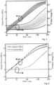
Figs. 5-6 show measurement results. -
Fig. 7 is a schematic circuit diagram of a bias circuit. - It should be emphasized that the term "comprises/comprising" when used in this disclosure is taken to specify the presence of stated features, integers, steps, or components, but does not preclude the presence or addition of one or more other features, integers, steps, components, or groups thereof.
- Adaptive bias is used in embodiments of the present disclosure to adjust the bias level when the input signal amplitude changes. In a class-A/AB Power amplifier (PA) this may for instance mean to increase the bias current as the input signal amplitude goes up.
- Adaptive bias can reduce amplitude to amplitude (AM - AM) distortion, which effectively means an increase in output referred 1 dB compression point (OP1dB) and saturated output power (Psat). It can also be a way to reduce the power consumption when delivering low output power.
-
Fig. 1 illustrates a communication environment wherein embodiments of the present disclosure may be employed. Awireless communication device 1, orwireless device 1 for short, of a cellular communications system is in wireless communication with aradio base station 2 of the cellular communications system. Thewireless device 1 may be what is generally referred to as a user equipment (UE). Thewireless devices 1 is depicted inFig. 1 as a mobile phone, but may be any kind of device with cellular communication capabilities, such as a tablet or laptop computer, machine-type communication (MTC) device, or similar. Furthermore, a cellular communications system is used as an example throughout this disclosure. However, embodiments of the present disclosure may be applicable in other types of systems as well, such as but not limited to WiFi systems. - The
radio base station 2 andwireless device 1 are examples of what in this disclosure is generically referred to as communication apparatuses. Embodiments are described below in the context of a communication apparatus in the form of theradio base station 2 orwireless device 1. However, other types of communication apparatuses can be considered as well, such as a WiFi access point or WiFi enabled device. -
Fig. 2 is a block diagram of an embodiment of atransceiver circuit 10, which can be comprised in a communication apparatus, such as theradio base station 2 or thewireless device 1. In the embodiment illustrated inFig. 2 , thetransceiver circuit 10 comprises a digital signal processing (DSP)circuit 15. TheDSP circuit 15 may e.g. be what is commonly referred to as baseband processor. TheDSP circuit 15 may e.g. be configured to perform various digital signal processing tasks, such as one or more of coding, decoding, modulation, demodulation, fast Fourier transform (FFT), inverse FFT (IFFT), mapping, demapping, etc. - Furthermore, in the embodiment illustrated in
Fig. 2 , thetransceiver circuit 10 comprises atransmitter circuit 20. Thetransmitter circuit 20 comprises a digital-to-analog converter (DAC) 25. TheDAC 25 is connected to theDSP circuit 15 and configured to receive, as an input signal of theDAC 25, a digital representation of a signal to be transmitted from theDSP circuit 15. TheDAC 25 is further configured to convert the signal to be transmitted to an analog representation, which is an output signal of theDAC 25. Thetransmitter circuit 20 also comprises a transmitter (Tx) frontend (FE)circuit 30 connected between theDAC 25 and anantenna 35. TheTx FE circuit 30 is configured to transform the output signal from theDAC 25 to a format suitable for transmission via theantenna 35. This may include operations such as frequency upconversion, filtering, and/or amplification. TheTx FE circuit 30 may comprise one or more mixers, filters, and/or amplifiers. The design of such Tx FE circuits is, per se, well known to a person skilled in the field of radio transceiver design and is not discussed herein in any further detail. TheTx FE circuit 30 typically also comprises a power amplifier (PA) configured to feed the signal to be transmitted into theantenna 35. Embodiments of a bias circuit for such a PA are presented in this disclosure. Furthermore, embodiments of a PA circuit comprising said bias circuit and a PA are also presented in this disclosure. - Moreover, in the embodiment illustrated in
Fig. 2 , thetransceiver circuit 10 comprises areceiver circuit 40. Thereceiver circuit 40 comprises a receiver (Rx)FE circuit 45 connected to theantenna 35. Furthermore, thereceiver circuit 40 comprises anADC 50. TheADC 50 is connected between theRx FE circuit 45 and theDSP circuit 15. TheRx FE circuit 45 is configured to transform a signal received via theantenna 35 to a format suitable to be input to theADC 50. This may include operations such as frequency downconversion, filtering, and/or amplification. TheRx FE circuit 45 may comprise one or more mixers, filters, and/or amplifiers, such as low-noise amplifiers (LNAs), to perform such operations. The design of such Rx FE circuits is, per se, well known to a person skilled in the field of radio transceiver design, and is not discussed herein in any further detail. TheADC 50 is configured to receive its (analog) input signal from the Rx FE circuit, and convert it to a digital representation to generate the digital output signal of theADC 50. This digital output signal of theADC 50 is input to theDSP circuit 15 for further digital signal processing. -
Fig. 3 is a schematic circuit diagram of aPA 100 that can be used in conjunction with embodiments of the above-mentioned bias circuit. It should be noted that the embodiment of thePA 100 illustrated inFig. 3 is merely an example, and that other types of PAs may be used together with the bias circuit as well. - According to the embodiment illustrated in
Fig. 3 , thePA 100 comprises an input stage of common source type. Said input stage comprises a differential pair ofinput transistors MCS 1 and MCS2, which are configured to be biased with a bias voltage Vbias at their gate terminals. The bias voltage Vbias may be supplied to the gate terminals of MCS1 and MCS2 in many different ways. In the embodiment illustrated inFig. 3 , thePA 100 comprises a first transformer T1. A secondary winding of the first transformer T1 is connected between the gate terminals of MCS1 and MCS2. The first transformer T1 is configured to receive the bias voltage at a center tap CT of the secondary winding. Furthermore, the first transformer T1 is configured to receive an input signal PAin of thePA 100 across a primary winding. InFig. 3 , the source terminals of MCS1 and MCS2 are connected to a first supply terminal (ground, or "GND"). - As illustrated in
Fig. 3 , thePA 100 may comprise additional transistor stages. For instance, inFig. 3 , thePA 100 comprises a common gate stage connected to the common source input stage. Said common gate stage comprises a differential pair of transistors MCG1 and MCG2. MCG1 and MCG2 acts as cascode transistors for MCS1 and MCS2. InFig. 3 , MCG1 and MCG2 are biased with a bias voltage CGbias at their gate terminals. - As illustrated in
Fig. 3 , thePA 100 may further comprise a second transformer T2. InFig. 3 , the second transformer T2 has a primary winding connected between the drain terminal of MCG1 and the drain terminal of MCG2. A center tap of the primary winding of D1 is connected to a second supply terminal ("VDD"). - Furthermore, In
Fig. 3 , the second transformer T2 is configured to generate an output PAout of thePA 100 across a secondary winding. - As illustrated in
Fig. 3 , thePA 100 may comprise further components, such as internal feedback capacitors C10 and C11, capacitors C8 and C9, and resistors R8 and R9. -
Fig. 4 is a schematic circuit diagram of abias circuit 200 according to embodiments of the present disclosure. Thebias circuit 200 is configured to generate the bias voltage Vbias, in a manner which is adaptive to the input signal of thePA 100. This enables an increase of OP1dB and Psat compared with a constant bias. - According to the embodiment illustrated in
Fig. 4 , thebias circuit 200 comprises a first transistor M1 having its drain terminal and its gate terminal connected to a first circuit node, labeled x, and its source terminal connected to a first supply terminal, labeled GND. Furthermore, thebias circuit 200 comprises a first current source, labeled I1, connected to the node x. Moreover, the bias circuit comprises a first resistor R1 connected between the node x and a second circuit node, labeled y. - According to the embodiment illustrated in
Fig. 4 , thebias circuit 200 comprises a second transistor M2 configured to receive a first component RFinp of a differential input signal to thePA 100 at its gate terminal. M2 has its drain terminal connected to the node y and its source terminal connected to a second supply terminal, labeled VDD. Similarly, according to the embodiment illustrated inFig. 4 , thebias circuit 200 comprises a third transistor M3 configured to receive a second component RFinn of the differential input signal to the PA at its gate terminal. M3 also has its drain terminal connected to the node y and its source terminal connected to VDD. The gate terminals of M2 and M3 are configured to be biased by a first voltage V1. This can be accomplished in many different ways. InFig. 4 , V1 is supplied to the gate terminals of M2 and M3 via resistors R2 and R3, respectively. RFinp and RFinn are supplied to the gate terminals of M2 and M3, respectively, via capacitors C2 and C3, respectively. - Let RFin denote the differential signal whose components are RFinn and RFinp. RFin may be the same signal as PAin (
Fig. 3 ). Hence, the capacitors C2 and C1 (Fig. 4 ) may be connected to the ends of the primary winding of the first transformer T1. In some embodiments RFin (Fig. 4 ) may be derived from PAin, e.g. via intervening circuit elements. In some embodiments, PAin may be derived from RFin, e.g. via intervening circuit elements. In some embodiments, PAin and RFin may both be derived from a common signal. - As indicated in
Fig. 4 , thebias circuit 200 may comprise a first capacitor C1 connected between the node x and the first supply terminal GND. - Furthermore, as indicated in
Fig. 4 , thebias circuit 200 is configured to generate the bias voltage Vbias at the node y. - As mentioned above, Vbias may be a bias voltage for gate terminals of input transistors, such as MCS1 and MCS2 (
Fig. 3 ) of thePA 100. - As illustrated with measurement results below, the
bias circuit 100 has a "knee-shaped" characteristic. Qualitatively speaking, for input magnitudes below a "knee", or threshold level, Vbias is approximately constant. For input magnitudes above the threshold level, Vbias increases approximately linearly with increasing input magnitude. For input magnitudes around the threshold level, there is a gradual increase of the slope of Vbias vs. input magnitude. - The location of the "knee", i.e. the threshold level, depends on the value of V1. According to some embodiments, V1 is digitally controllable. For instance, V1 may be generated by a DAC (not shown). This enables controlling the above-mentioned threshold level.
- The slope of Vbias vs the input magnitude depends on the resistance of R1. In some embodiments, the resistance of the R1 is digitally controllable. This enables controlling said slope of Vbias vs the input magnitude.
-
Figs. 5 and 6 show measurement results from a particular implementation of aPA 100 of the type illustrated inFig. 3 and a particular implementation of abias circuit 200 of the type illustrated inFig. 4 implemented in a 22nm FD (Fully Depleted) SOI (Silicon-on-Insulator) CMOS (Complementary Metal Oxide Semiconductor) manufacturing process. ThePA 100 used in the measurements is designed to operate at input frequencies around 27 GHz. The voltage V1 is controllable via 3 bits, i.e. has 8 different possible levels. Similarly, the resistance of R1 is controllable via 3 bits, i.e. said resistance has 8 different possible values. In total, there are thus 8x8=64 different settings. -
Figs. 5 and 6 illustrate how the output power (left y-axis) and Vbias (right y-axis, called CS bias voltage inFigs. 5 and 6 ) varies with the input magnitude (x-axis, labeled "DAC value" to indicate that it is the input signal level of the Tx DAC that generates the PA input). -
Fig. 5 plots the output power and Vbias for all 64 different combinations of V1 and the resistance of R1. As can be seen, there is a range of different settings, which allows Vbias to be controlled such that it starts to increase at the input level (i.e. the above-mentioned threshold level) where the PA output stage starts to compress, and that it increases with a slope that compensates the gain compression at higher input signal levels. As described above, to a first approximation, the starting point (or threshold level) can be controlled by the voltage V1, effectively setting at which input amplitude the rectifying transistor pair M2 and M3 will start to conduct current. As also discussed above, the slope of the increase in Vbias can be set with the digitally controlled resistor R1, transforming the DC current from the transistor pair M2 and M3 into a DC voltage. -
Fig. 6 compares the adaptive bias for a fixed setting of V1 and R1 with a case with a constant bias (i.e. a constant Vbias). As can be seen, by using the adaptive bias, an increase in both OP1dB and Psat can be obtained compared with when a constant bias voltage Vbias is used. - When adjusting the two tuning parameters, i.e. the V1 and the resistance of R1, it may be desirable to control the threshold level and the slope of Vbias relatively independently. It may also be also desirable that the output impedance of the
bias circuit 200 is relatively independent on the input magnitude, and that the voltage across the transistor M1 remains relatively constant at all input magnitudes to minimize the risk for memory effects.Fig. 7 illustrates an embodiment of thebias circuit 200 that has improved such properties in comparison with the embodiment illustrated inFig. 4 . InFig. 7 , thebias circuit 200 comprises a fourth transistor M4 having its gate terminal connected to a third circuit node z, its drain terminal connected to the first circuit node x, and its source terminal connected to the first supply terminal ("GND"). Qualitatively speaking, the transistor M4 can be used to subtract the signal-dependent current generated by M2 and M3 from the drain of M1, such that the drain current of M1 is relatively constant, independently of input magnitude. This can be obtained by the use of a "replica rectifier circuit" 250, whose output current is subtracted by a current mirror from the drain terminal of M1. M4 is the output side of that current mirror. Effectively the amplitude dependent current then flows in the programmable resistor R1, but not in the diode connected transistor M1, where ideally only the input reference current I1 will flow. The voltage across M1 will then remain relatively constant, and so will its impedance. - According to some embodiments, the
bias circuit 200 thus comprises (in said replica rectifier circuit 250) a fifth transistor M5 having its drain terminal and its gate terminal connected to the node z and its source terminal connected to the first supply terminal ("GND"). M5 is the input side of the above-mentioned current mirror. Furthermore, thebias circuit 200 comprises (in said replica rectifier circuit 250) a sixth transistor M6 configured to receive the first component RFinp of the differential input signal to the PA at its gate terminal, having its drain terminal connected to the node z and its source terminal connected to the second supply terminal ("VDD"). Moreover, thebias circuit 200 comprises (in said replica rectifier circuit 250) a seventh transistor M7 configured to receive the second component RFinn of the differential input signal to the PA at its gate terminal, having its drain terminal connected to the node z and its source terminal connected to the second supply terminal ("VDD"). M6 and M7 mimics the operation of M2 and M3. - The gate terminals of M6 and M7 may be configured to be biased with V1, e.g. via resistors R6 and R7, respectively, as illustrated in
Fig. 7 . Furthermore, RFinp and RFinn may be supplied to the gate terminals of M6 and M7, respectively, via capacitors C6 and C7, respectively. - In the embodiments illustrated in the drawings, the second supply terminal ("VDD") is configured to be supplied with a higher electrical potential than the first supply terminal ("GND"). For instance, GND may correspond to an electrical potential of 0V, and VDD may correspond to a positive supply voltage level. Furthermore, M1, M4, and M5 are NMOS transistors. Moreover, M2, M3, M6, and M7 are PMOS transistors. These embodiments are suitable to generate the bias voltage Vbias for the
PA 100 when the input transistors of the PA 100 (such as MCS1 and MCS2 inFig. 3 ) are NMOS transistors. - In other embodiments, a complementary implementation can be used, where connections to GND and VDD are interchanged, and PMOS transistors are replaced with NMOS transistors, and vice versa. In such an embodiment, the second supply terminal would be configured to be supplied with a lower electrical potential than the first supply terminal. For instance, GND may still correspond to an electrical potential of 0V, and VDD may still correspond to a positive supply voltage level, but GND may be connected to the second supply terminal and VDD to the first supply terminal. Furthermore, in such embodiments M1, and where applicable, M4 and M5, would be PMOS transistors. Moreover, M2 and M3, and where applicable, M6 and M7 would be NMOS transistors. Such embodiments would be suitable to generate the bias voltage Vbias for the
PA 100 in embodiments where the input transistors of thePA 100 are PMOS transistors. Such an embodiment of thePA 100 can e.g. be obtained as a complementary implementation of that inFig. 3 , by interchanging connections to GND and VDD, and by replacing NMOS transistors MCS1 and MCS2 (and MCG1 and MCG2) with PMOS transistors. - According to some embodiments, there is provided a PA circuit comprising an embodiment of the
bias circuit 200 and a PA, such as an embodiment of thePA 100, configured to be biased with said bias voltage Vbias. - Embodiments of the PA circuit, including the
bias circuit 200 and the PA, are suitable for integration (either fully or in part) on an integrated circuit. Thus, according to some embodiments, there is provided an integrated circuit comprising the PA circuit. - The PA circuit may be comprised in an electronic apparatus. The electronic apparatus may e.g. be a communication apparatus, such as the
wireless communication device 1 or base station 2 (Fig. 1 ). For instance, the PA circuit may be included in theTxFE circuit 30 of the transceiver circuit 10 (Fig. 2 ). Thetransceiver circuit 10 may in turn be included in the electronic apparatus. - Embodiments of the
adaptive bias circuit 200 are designed to track an envelope of the input signal to the PA. This is advantageous compared with tracking the output signal amplitude. One reason is that tracking the output signal would result in a loop, with potential instability. The loop is formed since the output signal amplitude depends on the bias, which is controlled by the output signal amplitude. Tracking the input amplitude avoids that issue. Another problem of tracking the output signal is that when the amplifier starts to saturate, and the bias voltage needs to increase more rapidly to compensate, the output signal amplitude increases more slowly with input, so in contrast to what is needed, a less effective bias voltage steepness may be obtained. - The disclosure above refers to specific embodiments. However, other embodiments than the above described are possible. For example, the PA circuit may be used in other types of electronic apparatuses than communication apparatuses. The different features of the embodiments may be combined in other combinations than those described.
- For completeness, the subject matter of the claims of the parent application (application number 19761843.2) as filed is provided in the following list of examples as part of this detailed description.
-
- Example 1. A bias circuit (200) for a power amplifier, PA, (100) comprising
- a first transistor (M1) having its drain terminal and its gate terminal connected to a first circuit node (x) and its source terminal connected to a first supply terminal (GND);
- a first current source (I1) connected to the first circuit node (x);
- a first resistor (R1) connected between the first circuit node (x) and a second circuit node (y);
- a second transistor (M2) configured to receive a first component (RFinp) of a differential input signal to the PA at its gate terminal, having its drain terminal connected to the second circuit node (y) and its source terminal connected to a second supply terminal (VDD); and
- a third transistor (M3) configured to receive a second component (RFinn) of the differential input signal to the PA at its gate terminal, having its drain terminal connected to the second circuit node (y) and its source terminal connected to a second supply terminal (VDD); wherein
- the gate terminals of the second transistor (M2) and the third transistor (M3) are configured to be biased by a first voltage (V1); and
- the bias circuit is configured to generate a bias voltage (Vbias) for the PA (100) at the second circuit node (y).
- Example 2. The bias circuit (200) of example 1, wherein the bias voltage (Vbias) for the PA (100) is a bias voltage (Vbias) for gate terminals of input transistors (MCS1, MCS2) of the PA (100).
- Example 3. The bias circuit (200) of example 1 or 2, wherein the first voltage (V1) is digitally controllable.
- Example 4. The bias circuit (200) of any one of the preceding examples, wherein a resistance of the first resistor (R1) is digitally controllable.
- Example 5. The bias circuit (200) of any one of the preceding examples, comprising a first capacitor (C1) connected between the first circuit node (x) and the first supply terminal (GND).
- Example 6. The bias circuit (200) of any one of the preceding examples, comprising
a fourth transistor (M4) having its gate terminal connected to a third circuit node (z), its drain terminal connected to the first circuit node (x), and its source terminal connected to the first supply terminal (GND). - Example 7. The bias circuit (200) of example 6, comprising
- a fifth transistor (M5) having its drain terminal and its gate terminal connected to the third circuit node (z) and its source terminal connected to the first supply terminal (GND);
- a sixth transistor (M6) configured to receive the first component (RFinp) of a differential input signal to the PA at its gate terminal, having its drain terminal connected to the third circuit node (z) and its source terminal connected to the second supply terminal (VDD); and
- a seventh transistor (M3) configured to receive the second component (RFinn) of the differential input signal to the PA at its gate terminal, having its drain terminal connected to the third circuit node (z) and its source terminal connected to the second supply terminal (VDD).
- Example 8. The bias circuit (200) of example 7, wherein the gate terminals of the sixth transistor (M6) and the seventh transistor (M7) are configured to be biased by the first voltage (V1).
- Example 9. The bias circuit (200) of any preceding example, wherein the second supply terminal (VDD) is configured to be supplied with a higher electrical potential than the first supply terminal (GND);
- the first transistor (M1) is an NMOS transistor; and
- the second transistor (M2) and the third transistor (M3) are PMOS transistors.
- Example 10. The bias circuit (200) of any one of the examples 1-8, wherein the second supply terminal is configured to be supplied with a lower electrical potential than the first supply terminal;
- the first transistor (M1) is a PMOS transistor; and
- the second transistor (M2) and the third transistor (M3) are NMOS transistors.
- Example 11. A PA circuit comprising
- the bias circuit (200) of any preceding example; and
- a PA (100) configured to be biased with said bias voltage.
- Example 12. The PA circuit of example 11, wherein the PA (100) comprises
an input stage of common source type, wherein input transistors (MCS1, MCS2) of the input stage are configured to be biased with the bias voltage (Vbias) at their gate terminals. - Example 13. The PA circuit of example 12, wherein the PA (100) comprises a first transformer (T1) configured to receive the input signal of the PA (100) across a primary winding, having a secondary winding connected between the gate terminals of the input transistors (MCS1, MCS2) of the input stage, and configured to receive the bias voltage at a center tap (CT) of the secondary winding.
- Example 14. An integrated circuit comprising the PA circuit of any one of the examples 11-13.
- Example 15. An electronic apparatus (1, 2) comprising the PA circuit of any one of the examples 11 - 13.
- Example 16. The electronic apparatus (1, 2) of example 15, wherein the electronic apparatus is a communication apparatus.
- Example 17. The electronic apparatus (1) of example 16, wherein the communication apparatus is a wireless communication device for a cellular communications system.
- Example 18. The electronic apparatus (2) of example 16, wherein the communication apparatus is a base station for a cellular communications system.
Claims (15)
- A bias circuit (200) for a power amplifier, PA, (100) comprisinga first transistor (M1) having its drain terminal and its gate terminal connected to a first circuit node (x) and its source terminal connected to a first supply terminal (GND);a first current source (I1) connected to the first circuit node (x);a first resistor (R1) connected between the first circuit node (x) and a second circuit node (y);a second transistor (M2) configured to receive a first component (RFinp) of a differential input signal to the PA at its gate terminal, having its drain terminal connected to the second circuit node (y) and its source terminal connected to a second supply terminal (VDD); anda third transistor (M3) configured to receive a second component (RFinn) of the differential input signal to the PA at its gate terminal, having its drain terminal connected to the second circuit node (y) and its source terminal connected to a second supply terminal (VDD); whereinthe gate terminals of the second transistor (M2) and the third transistor (M3) are configured to be biased by a first voltage (V1);the bias circuit is configured to generate a bias voltage (Vbias) for the PA (100) at the second circuit node (y);the first voltage (V1) is digitally controllable; anda resistance of the first resistor (R1) is digitally controllable.
- The bias circuit (200) of claim 1, wherein the bias voltage (Vbias) for the PA (100) is a bias voltage (Vbias) for gate terminals of input transistors (MCS1, MCS2) of the PA (100).
- The bias circuit (200) of claim 1 or 2, comprising a first capacitor (C1) connected between the first circuit node (x) and the first supply terminal (GND).
- The bias circuit (200) of any one of the preceding claims, comprising
a fourth transistor (M4) having its gate terminal connected to a third circuit node (z), its drain terminal connected to the first circuit node (x), and its source terminal connected to the first supply terminal (GND). - The bias circuit (200) of claim 4, comprisinga fifth transistor (M5) having its drain terminal and its gate terminal connected to the third circuit node (z) and its source terminal connected to the first supply terminal (GND);a sixth transistor (M6) configured to receive the first component (RFinp) of a differential input signal to the PA at its gate terminal, having its drain terminal connected to the third circuit node (z) and its source terminal connected to the second supply terminal (VDD); anda seventh transistor (M3) configured to receive the second component (RFinn) of the differential input signal to the PA at its gate terminal, having its drain terminal connected to the third circuit node (z) and its source terminal connected to the second supply terminal (VDD).
- The bias circuit (200) of claim 5, wherein the gate terminals of the sixth transistor (M6) and the seventh transistor (M7) are configured to be biased by the first voltage (V1).
- The bias circuit (200) of any preceding claim, wherein
either- the second supply terminal (VDD) is configured to be supplied with a higher electrical potential than the first supply terminal (GND);- the first transistor (M1) is an NMOS transistor; and- the second transistor (M2) and the third transistor (M3) are PMOS transistors;or- the second supply terminal is configured to be supplied with a lower electrical potential than the first supply terminal;- the first transistor (M1) is a PMOS transistor; and- the second transistor (M2) and the third transistor (M3) are NMOS transistors. - A PA circuit comprisingthe bias circuit (200) of any preceding claim; anda PA (100) configured to be biased with said bias voltage.
- The PA circuit of claim 8, wherein the PA (100) comprises
an input stage of common source type, wherein input transistors (MCS1, MCS2) of the input stage are configured to be biased with the bias voltage (Vbias) at their gate terminals. - The PA circuit of claim 9, wherein the PA (100) comprises a first transformer (T1) configured to receive the input signal of the PA (100) across a primary winding, having a secondary winding connected between the gate terminals of the input transistors (MCS1, MCS2) of the input stage, and configured to receive the bias voltage at a center tap (CT) of the secondary winding.
- An integrated circuit comprising the PA circuit of any one of the claims 8-10.
- An electronic apparatus (1, 2) comprising the PA circuit of any one of the claims 8 - 10.
- The electronic apparatus (1, 2) of claim 12, wherein the electronic apparatus is a communication apparatus.
- The electronic apparatus (1) of claim 13, wherein the communication apparatus is a wireless communication device for a cellular communications system.
- The electronic apparatus (2) of claim 13, wherein the communication apparatus is a base station for a cellular communications system.
Applications Claiming Priority (3)
| Application Number | Priority Date | Filing Date | Title |
|---|---|---|---|
| US201962790767P | 2019-01-10 | 2019-01-10 | |
| EP19761843.2A EP3909127B1 (en) | 2019-01-10 | 2019-08-29 | Bias circuit and power amplifier circuit |
| PCT/EP2019/073046 WO2020143934A1 (en) | 2019-01-10 | 2019-08-29 | Bias circuit and power amplifier circuit |
Related Parent Applications (1)
| Application Number | Title | Priority Date | Filing Date |
|---|---|---|---|
| EP19761843.2A Division EP3909127B1 (en) | 2019-01-10 | 2019-08-29 | Bias circuit and power amplifier circuit |
Publications (4)
| Publication Number | Publication Date |
|---|---|
| EP4398483A2 true EP4398483A2 (en) | 2024-07-10 |
| EP4398483A3 EP4398483A3 (en) | 2024-10-16 |
| EP4398483B1 EP4398483B1 (en) | 2025-10-01 |
| EP4398483C0 EP4398483C0 (en) | 2025-10-01 |
Family
ID=67809490
Family Applications (2)
| Application Number | Title | Priority Date | Filing Date |
|---|---|---|---|
| EP24177413.2A Active EP4398483B1 (en) | 2019-01-10 | 2019-08-29 | Bias circuit and power amplifier circuit |
| EP19761843.2A Active EP3909127B1 (en) | 2019-01-10 | 2019-08-29 | Bias circuit and power amplifier circuit |
Family Applications After (1)
| Application Number | Title | Priority Date | Filing Date |
|---|---|---|---|
| EP19761843.2A Active EP3909127B1 (en) | 2019-01-10 | 2019-08-29 | Bias circuit and power amplifier circuit |
Country Status (4)
| Country | Link |
|---|---|
| US (2) | US11990875B2 (en) |
| EP (2) | EP4398483B1 (en) |
| CN (1) | CN113273079B (en) |
| WO (1) | WO2020143934A1 (en) |
Families Citing this family (4)
| Publication number | Priority date | Publication date | Assignee | Title |
|---|---|---|---|---|
| US12519427B2 (en) | 2020-05-14 | 2026-01-06 | Telefonaktiebolaget Lm Ericsson (Publ) | Envelope controlled biasing of an auxiliary transmitter of a doherty power amplifier |
| EP4169159B1 (en) | 2020-06-22 | 2025-09-24 | Telefonaktiebolaget LM ERICSSON (PUBL) | Transmitter circuit |
| WO2022103496A1 (en) | 2020-11-16 | 2022-05-19 | Qorvo Us, Inc. | Power management circuit operable with multiple supply voltages |
| WO2025223675A1 (en) | 2024-04-26 | 2025-10-30 | Telefonaktiebolaget Lm Ericsson (Publ) | Amplifier circuit |
Citations (1)
| Publication number | Priority date | Publication date | Assignee | Title |
|---|---|---|---|---|
| US9300253B2 (en) | 2013-11-08 | 2016-03-29 | Socionext Inc. | Amplifier |
Family Cites Families (26)
| Publication number | Priority date | Publication date | Assignee | Title |
|---|---|---|---|---|
| US4225897A (en) * | 1979-01-29 | 1980-09-30 | Rca Corporation | Overcurrent protection circuit for power transistor |
| US5023937A (en) | 1989-05-09 | 1991-06-11 | Motorola, Inc. | Transmitter with improved linear amplifier control |
| JP2967699B2 (en) | 1995-03-06 | 1999-10-25 | 日本電気株式会社 | Transmission device |
| CA2242724C (en) * | 1998-07-09 | 2002-01-01 | Ibm Canada Limited-Ibm Canada Limitee | Adaptive bandwidth stabilization for an integrated circuit amplifier |
| US6275685B1 (en) | 1998-12-10 | 2001-08-14 | Nortel Networks Limited | Linear amplifier arrangement |
| US6522111B2 (en) * | 2001-01-26 | 2003-02-18 | Linfinity Microelectronics | Linear voltage regulator using adaptive biasing |
| DE102005013880B3 (en) | 2005-03-24 | 2006-04-20 | Infineon Technologies Ag | Signals predistortion method, involves selecting table from set of two tables based on determined operating condition, and selecting pre distortion coefficient from selected table based on performance word and component |
| US7443237B1 (en) * | 2006-06-02 | 2008-10-28 | Linear Technology Corporation | Folded cascode amplifier having improved slew performance |
| US7873980B2 (en) * | 2006-11-02 | 2011-01-18 | Redmere Technology Ltd. | High-speed cable with embedded signal format conversion and power control |
| US7639081B2 (en) * | 2007-02-06 | 2009-12-29 | Texas Instuments Incorporated | Biasing scheme for low-voltage MOS cascode current mirrors |
| US7733182B2 (en) * | 2008-10-31 | 2010-06-08 | Agere Systems Inc. | Hybrid class AB super follower |
| CN102257735B (en) | 2008-12-17 | 2015-07-22 | 翔跃通信公司 | Base station with coordinated multiple air-interface operations |
| JP5107272B2 (en) * | 2009-01-15 | 2012-12-26 | 株式会社東芝 | Temperature compensation circuit |
| CN106411279B (en) | 2011-11-02 | 2019-04-12 | 马维尔国际贸易有限公司 | Circuit for difference amplifier |
| CN202931370U (en) | 2012-11-01 | 2013-05-08 | 中国电子科技集团公司第五十研究所 | RF predistortion circuit |
| US8970301B2 (en) * | 2013-05-20 | 2015-03-03 | Analog Devices, Inc. | Method for low power low noise input bias current compensation |
| WO2015103768A1 (en) * | 2014-01-10 | 2015-07-16 | Silicon Image, Inc. | Linear regulator with improved power supply ripple rejection |
| TWI531159B (en) | 2014-01-16 | 2016-04-21 | 國立臺灣科技大學 | Transconductance amplifier, programmable recombination fully differential voltage sense amplifier, and programmable recombination fully differential capacitance sense amplifier |
| US9214933B2 (en) * | 2014-02-25 | 2015-12-15 | Taiwan Semiconductor Manufacturing Company, Ltd. | Input/output circuit |
| US9391569B2 (en) * | 2014-03-31 | 2016-07-12 | Qualcomm Incorporated | Multi-stage switched-capacitor DC blocking circuit for audio frontend |
| US10153794B2 (en) | 2016-12-02 | 2018-12-11 | Mediatek, Inc. | Transmitter, communication unit and method for limiting spectral re-growth |
| US10333478B1 (en) * | 2017-12-20 | 2019-06-25 | Texas Instruments Incorporated | Slew boost disable for an operational amplifier |
| US10571945B2 (en) * | 2018-02-21 | 2020-02-25 | Atlazo, Inc. | Low power regulator circuits, systems and methods regarding the same |
| US10819303B1 (en) * | 2019-10-17 | 2020-10-27 | Qualcomm Incorporated | Amplifier with gain boosting |
| US11431297B2 (en) | 2020-03-04 | 2022-08-30 | Qorvo Us, Inc. | Envelope tracking power amplifier apparatus with predistortion |
| US12261577B2 (en) * | 2021-06-23 | 2025-03-25 | Qualcomm Incorporated | Amplifier peak detection |
-
2019
- 2019-08-29 WO PCT/EP2019/073046 patent/WO2020143934A1/en not_active Ceased
- 2019-08-29 US US17/421,289 patent/US11990875B2/en active Active
- 2019-08-29 CN CN201980088536.4A patent/CN113273079B/en active Active
- 2019-08-29 EP EP24177413.2A patent/EP4398483B1/en active Active
- 2019-08-29 EP EP19761843.2A patent/EP3909127B1/en active Active
-
2024
- 2024-04-15 US US18/635,728 patent/US12283925B2/en active Active
Patent Citations (1)
| Publication number | Priority date | Publication date | Assignee | Title |
|---|---|---|---|---|
| US9300253B2 (en) | 2013-11-08 | 2016-03-29 | Socionext Inc. | Amplifier |
Non-Patent Citations (3)
| Title |
|---|
| J. Y. LIUR. BERENGUERM. F. CHANG: "Millimeter-Wave Self-Healing Power Amplifier With Adaptive Amplitude and Phase Linearization in 65-nm CMOS", IEEE TRANSACTIONS ON MICROWAVE THEORY AND TECHNIQUES, vol. 60, no. 5, May 2012 (2012-05-01), pages 1342 - 1352, XP011442425, DOI: 10.1109/TMTT.2012.2189119 |
| S. KOUSAIK. ONIZUKAT. YAMAGUCHIY. KURIYAMAM. NAGAOKA: "A 28.3 mW PA-Closed Loop for Linearity and Efficiency Improvement Integrated in a +27.1 dBm WCDMA CMOS Power Amplifier", IEEE JOURNAL OF SOLID-STATE CIRCUITS, vol. 47, no. 12, December 2012 (2012-12-01), pages 2964 - 2973 |
| S. WENGY. LEET. CHENJ. Y. LIU: "A 60-GHz Adaptively Biased Power Amplifier with Predistortion Linearizer in 90-nm CMOS", 2018 IEEE/MTT-S INTERNATIONAL MICROWAVE SYMPOSIUM - IMS, 2018, pages 651 - 654, XP033388078, DOI: 10.1109/MWSYM.2018.8439439 |
Also Published As
| Publication number | Publication date |
|---|---|
| EP4398483B1 (en) | 2025-10-01 |
| EP4398483C0 (en) | 2025-10-01 |
| CN113273079B (en) | 2024-03-22 |
| EP3909127B1 (en) | 2024-05-29 |
| US12283925B2 (en) | 2025-04-22 |
| EP4398483A3 (en) | 2024-10-16 |
| WO2020143934A1 (en) | 2020-07-16 |
| US20220123697A1 (en) | 2022-04-21 |
| EP3909127A1 (en) | 2021-11-17 |
| CN113273079A (en) | 2021-08-17 |
| US11990875B2 (en) | 2024-05-21 |
| US20240267011A1 (en) | 2024-08-08 |
Similar Documents
| Publication | Publication Date | Title |
|---|---|---|
| US7421254B2 (en) | High linearity, high efficiency power amplifier with DSP assisted linearity optimization | |
| CN111064438B (en) | Analog predistortion circuit, power amplifier and radio frequency module | |
| US12283925B2 (en) | Bias circuit and power amplifier circuit | |
| US12237813B2 (en) | Power amplifier equalizer | |
| JP6644706B2 (en) | Circuit and method for biasing a power amplifier | |
| CN118117977B (en) | Linearization circuits, power amplifiers, chips and devices | |
| Onizuka et al. | A 1.9 GHz CMOS power amplifier with embedded linearizer to compensate AM-PM distortion | |
| US20250119105A1 (en) | Power Amplifier Linearizer | |
| US12255591B2 (en) | Temperature compensation bias circuit and power amplifier | |
| US11764738B2 (en) | Segmented power amplifier arrangements with feedforward adaptive bias circuits | |
| US11251753B2 (en) | Envelope tracking supply modulator with zero peaking and associated envelope tracking calibration method and system | |
| Lee et al. | A CMOS outphasing power amplifier with integrated single-ended Chireix combiner | |
| JP2010283556A (en) | High frequency amplifier, and high frequency module using the same | |
| EP1254509A1 (en) | Lineariser | |
| EP1526636A1 (en) | High linearity, high efficiency power amplifier with DSP assisted linearity optimization | |
| KR20170073459A (en) | Power amplifier and wireless communication apparatus | |
| Qin et al. | A 26-30GHz Digitally-Controlled Variable Gain Power Amplifier with Phase Compensation and Third Order Nonlinearity Cancellation Technique | |
| US12512796B2 (en) | Bias block for biasing transistors exhibiting non-linearity when designed for linear operation | |
| Mahoutı et al. | DESIGN OF A HIGH EFFICIENCY POWER AMPLIFIER FOR WIRELESS AND RADAR APPLICATIONS | |
| MAHOUTI et al. | DESIGN OF A HIGH EFFICIENTLY POWER AMPLIFIER FOR GSM APPLICATIONS | |
| Huang | CMOS-based amplitude and phase control circuits designed for multi-standard wireless communication systems |
Legal Events
| Date | Code | Title | Description |
|---|---|---|---|
| PUAI | Public reference made under article 153(3) epc to a published international application that has entered the european phase |
Free format text: ORIGINAL CODE: 0009012 |
|
| STAA | Information on the status of an ep patent application or granted ep patent |
Free format text: STATUS: THE APPLICATION HAS BEEN PUBLISHED |
|
| AC | Divisional application: reference to earlier application |
Ref document number: 3909127 Country of ref document: EP Kind code of ref document: P |
|
| AK | Designated contracting states |
Kind code of ref document: A2 Designated state(s): AL AT BE BG CH CY CZ DE DK EE ES FI FR GB GR HR HU IE IS IT LI LT LU LV MC MK MT NL NO PL PT RO RS SE SI SK SM TR |
|
| REG | Reference to a national code |
Ref country code: DE Ref legal event code: R079 Free format text: PREVIOUS MAIN CLASS: H03F0001220000 Ipc: H03F0001020000 Ref document number: 602019076566 Country of ref document: DE |
|
| PUAL | Search report despatched |
Free format text: ORIGINAL CODE: 0009013 |
|
| AK | Designated contracting states |
Kind code of ref document: A3 Designated state(s): AL AT BE BG CH CY CZ DE DK EE ES FI FR GB GR HR HU IE IS IT LI LT LU LV MC MK MT NL NO PL PT RO RS SE SI SK SM TR |
|
| RIC1 | Information provided on ipc code assigned before grant |
Ipc: H03F 1/22 20060101ALI20240906BHEP Ipc: H03F 3/45 20060101ALI20240906BHEP Ipc: H03F 3/213 20060101ALI20240906BHEP Ipc: H03F 1/02 20060101AFI20240906BHEP |
|
| STAA | Information on the status of an ep patent application or granted ep patent |
Free format text: STATUS: REQUEST FOR EXAMINATION WAS MADE |
|
| 17P | Request for examination filed |
Effective date: 20250326 |
|
| RIC1 | Information provided on ipc code assigned before grant |
Ipc: H03F 1/22 20060101ALI20250417BHEP Ipc: H03F 3/45 20060101ALI20250417BHEP Ipc: H03F 3/213 20060101ALI20250417BHEP Ipc: H03F 1/02 20060101AFI20250417BHEP |
|
| GRAP | Despatch of communication of intention to grant a patent |
Free format text: ORIGINAL CODE: EPIDOSNIGR1 |
|
| STAA | Information on the status of an ep patent application or granted ep patent |
Free format text: STATUS: GRANT OF PATENT IS INTENDED |
|
| INTG | Intention to grant announced |
Effective date: 20250523 |
|
| RIN1 | Information on inventor provided before grant (corrected) |
Inventor name: SJOELAND, HENRIK Inventor name: ELGAARD, CHRISTIAN |
|
| GRAS | Grant fee paid |
Free format text: ORIGINAL CODE: EPIDOSNIGR3 |
|
| GRAA | (expected) grant |
Free format text: ORIGINAL CODE: 0009210 |
|
| STAA | Information on the status of an ep patent application or granted ep patent |
Free format text: STATUS: THE PATENT HAS BEEN GRANTED |
|
| AC | Divisional application: reference to earlier application |
Ref document number: 3909127 Country of ref document: EP Kind code of ref document: P |
|
| AK | Designated contracting states |
Kind code of ref document: B1 Designated state(s): AL AT BE BG CH CY CZ DE DK EE ES FI FR GB GR HR HU IE IS IT LI LT LU LV MC MK MT NL NO PL PT RO RS SE SI SK SM TR |
|
| REG | Reference to a national code |
Ref country code: GB Ref legal event code: FG4D Ref country code: CH Ref legal event code: F10 Free format text: ST27 STATUS EVENT CODE: U-0-0-F10-F00 (AS PROVIDED BY THE NATIONAL OFFICE) Effective date: 20251001 |
|
| REG | Reference to a national code |
Ref country code: IE Ref legal event code: FG4D |
|
| REG | Reference to a national code |
Ref country code: DE Ref legal event code: R096 Ref document number: 602019076566 Country of ref document: DE |
|
| U01 | Request for unitary effect filed |
Effective date: 20251023 |
|
| U07 | Unitary effect registered |
Designated state(s): AT BE BG DE DK EE FI FR IT LT LU LV MT NL PT RO SE SI Effective date: 20251030 |
|
| PG25 | Lapsed in a contracting state [announced via postgrant information from national office to epo] |
Ref country code: ES Free format text: LAPSE BECAUSE OF FAILURE TO SUBMIT A TRANSLATION OF THE DESCRIPTION OR TO PAY THE FEE WITHIN THE PRESCRIBED TIME-LIMIT Effective date: 20251001 |
|
| PG25 | Lapsed in a contracting state [announced via postgrant information from national office to epo] |
Ref country code: NO Free format text: LAPSE BECAUSE OF FAILURE TO SUBMIT A TRANSLATION OF THE DESCRIPTION OR TO PAY THE FEE WITHIN THE PRESCRIBED TIME-LIMIT Effective date: 20260101 |
|
| PG25 | Lapsed in a contracting state [announced via postgrant information from national office to epo] |
Ref country code: HR Free format text: LAPSE BECAUSE OF FAILURE TO SUBMIT A TRANSLATION OF THE DESCRIPTION OR TO PAY THE FEE WITHIN THE PRESCRIBED TIME-LIMIT Effective date: 20251001 |
|
| PG25 | Lapsed in a contracting state [announced via postgrant information from national office to epo] |
Ref country code: RS Free format text: LAPSE BECAUSE OF FAILURE TO SUBMIT A TRANSLATION OF THE DESCRIPTION OR TO PAY THE FEE WITHIN THE PRESCRIBED TIME-LIMIT Effective date: 20260101 |
|
| PG25 | Lapsed in a contracting state [announced via postgrant information from national office to epo] |
Ref country code: IS Free format text: LAPSE BECAUSE OF FAILURE TO SUBMIT A TRANSLATION OF THE DESCRIPTION OR TO PAY THE FEE WITHIN THE PRESCRIBED TIME-LIMIT Effective date: 20260201 |
|
| PG25 | Lapsed in a contracting state [announced via postgrant information from national office to epo] |
Ref country code: CZ Free format text: LAPSE BECAUSE OF FAILURE TO SUBMIT A TRANSLATION OF THE DESCRIPTION OR TO PAY THE FEE WITHIN THE PRESCRIBED TIME-LIMIT Effective date: 20251001 |
|
| PG25 | Lapsed in a contracting state [announced via postgrant information from national office to epo] |
Ref country code: PL Free format text: LAPSE BECAUSE OF FAILURE TO SUBMIT A TRANSLATION OF THE DESCRIPTION OR TO PAY THE FEE WITHIN THE PRESCRIBED TIME-LIMIT Effective date: 20251001 |