EP4398429A2 - Red-green-blue, vertical-cavity, surface-emitting laser array - Google Patents
Red-green-blue, vertical-cavity, surface-emitting laser array Download PDFInfo
- Publication number
- EP4398429A2 EP4398429A2 EP23217092.8A EP23217092A EP4398429A2 EP 4398429 A2 EP4398429 A2 EP 4398429A2 EP 23217092 A EP23217092 A EP 23217092A EP 4398429 A2 EP4398429 A2 EP 4398429A2
- Authority
- EP
- European Patent Office
- Prior art keywords
- vcsel
- array
- wavelength range
- vcsels
- emit
- Prior art date
- Legal status (The legal status is an assumption and is not a legal conclusion. Google has not performed a legal analysis and makes no representation as to the accuracy of the status listed.)
- Pending
Links
Images




Classifications
-
- H—ELECTRICITY
- H01—ELECTRIC ELEMENTS
- H01S—DEVICES USING THE PROCESS OF LIGHT AMPLIFICATION BY STIMULATED EMISSION OF RADIATION [LASER] TO AMPLIFY OR GENERATE LIGHT; DEVICES USING STIMULATED EMISSION OF ELECTROMAGNETIC RADIATION IN WAVE RANGES OTHER THAN OPTICAL
- H01S5/00—Semiconductor lasers
- H01S5/40—Arrangement of two or more semiconductor lasers, not provided for in groups H01S5/02 - H01S5/30
- H01S5/42—Arrays of surface emitting lasers
- H01S5/423—Arrays of surface emitting lasers having a vertical cavity
- H01S5/426—Vertically stacked cavities
-
- H—ELECTRICITY
- H01—ELECTRIC ELEMENTS
- H01S—DEVICES USING THE PROCESS OF LIGHT AMPLIFICATION BY STIMULATED EMISSION OF RADIATION [LASER] TO AMPLIFY OR GENERATE LIGHT; DEVICES USING STIMULATED EMISSION OF ELECTROMAGNETIC RADIATION IN WAVE RANGES OTHER THAN OPTICAL
- H01S5/00—Semiconductor lasers
- H01S5/06—Arrangements for controlling the laser output parameters, e.g. by operating on the active medium
- H01S5/065—Mode locking; Mode suppression; Mode selection ; Self pulsating
- H01S5/0651—Mode control
- H01S5/0653—Mode suppression, e.g. specific multimode
- H01S5/0655—Single transverse or lateral mode emission
-
- H—ELECTRICITY
- H01—ELECTRIC ELEMENTS
- H01S—DEVICES USING THE PROCESS OF LIGHT AMPLIFICATION BY STIMULATED EMISSION OF RADIATION [LASER] TO AMPLIFY OR GENERATE LIGHT; DEVICES USING STIMULATED EMISSION OF ELECTROMAGNETIC RADIATION IN WAVE RANGES OTHER THAN OPTICAL
- H01S5/00—Semiconductor lasers
- H01S5/10—Construction or shape of the optical resonator, e.g. extended or external cavity, coupled cavities, bent-guide, varying width, thickness or composition of the active region
- H01S5/18—Surface-emitting [SE] lasers, e.g. having both horizontal and vertical cavities
- H01S5/183—Surface-emitting [SE] lasers, e.g. having both horizontal and vertical cavities having only vertical cavities, e.g. vertical cavity surface-emitting lasers [VCSEL]
- H01S5/18305—Surface-emitting [SE] lasers, e.g. having both horizontal and vertical cavities having only vertical cavities, e.g. vertical cavity surface-emitting lasers [VCSEL] with emission through the substrate, i.e. bottom emission
-
- H—ELECTRICITY
- H01—ELECTRIC ELEMENTS
- H01S—DEVICES USING THE PROCESS OF LIGHT AMPLIFICATION BY STIMULATED EMISSION OF RADIATION [LASER] TO AMPLIFY OR GENERATE LIGHT; DEVICES USING STIMULATED EMISSION OF ELECTROMAGNETIC RADIATION IN WAVE RANGES OTHER THAN OPTICAL
- H01S5/00—Semiconductor lasers
- H01S5/10—Construction or shape of the optical resonator, e.g. extended or external cavity, coupled cavities, bent-guide, varying width, thickness or composition of the active region
- H01S5/18—Surface-emitting [SE] lasers, e.g. having both horizontal and vertical cavities
- H01S5/183—Surface-emitting [SE] lasers, e.g. having both horizontal and vertical cavities having only vertical cavities, e.g. vertical cavity surface-emitting lasers [VCSEL]
- H01S5/18308—Surface-emitting [SE] lasers, e.g. having both horizontal and vertical cavities having only vertical cavities, e.g. vertical cavity surface-emitting lasers [VCSEL] having a special structure for lateral current or light confinement
-
- H—ELECTRICITY
- H01—ELECTRIC ELEMENTS
- H01S—DEVICES USING THE PROCESS OF LIGHT AMPLIFICATION BY STIMULATED EMISSION OF RADIATION [LASER] TO AMPLIFY OR GENERATE LIGHT; DEVICES USING STIMULATED EMISSION OF ELECTROMAGNETIC RADIATION IN WAVE RANGES OTHER THAN OPTICAL
- H01S5/00—Semiconductor lasers
- H01S5/10—Construction or shape of the optical resonator, e.g. extended or external cavity, coupled cavities, bent-guide, varying width, thickness or composition of the active region
- H01S5/18—Surface-emitting [SE] lasers, e.g. having both horizontal and vertical cavities
- H01S5/183—Surface-emitting [SE] lasers, e.g. having both horizontal and vertical cavities having only vertical cavities, e.g. vertical cavity surface-emitting lasers [VCSEL]
- H01S5/18308—Surface-emitting [SE] lasers, e.g. having both horizontal and vertical cavities having only vertical cavities, e.g. vertical cavity surface-emitting lasers [VCSEL] having a special structure for lateral current or light confinement
- H01S5/18311—Surface-emitting [SE] lasers, e.g. having both horizontal and vertical cavities having only vertical cavities, e.g. vertical cavity surface-emitting lasers [VCSEL] having a special structure for lateral current or light confinement using selective oxidation
-
- H—ELECTRICITY
- H01—ELECTRIC ELEMENTS
- H01S—DEVICES USING THE PROCESS OF LIGHT AMPLIFICATION BY STIMULATED EMISSION OF RADIATION [LASER] TO AMPLIFY OR GENERATE LIGHT; DEVICES USING STIMULATED EMISSION OF ELECTROMAGNETIC RADIATION IN WAVE RANGES OTHER THAN OPTICAL
- H01S5/00—Semiconductor lasers
- H01S5/10—Construction or shape of the optical resonator, e.g. extended or external cavity, coupled cavities, bent-guide, varying width, thickness or composition of the active region
- H01S5/18—Surface-emitting [SE] lasers, e.g. having both horizontal and vertical cavities
- H01S5/183—Surface-emitting [SE] lasers, e.g. having both horizontal and vertical cavities having only vertical cavities, e.g. vertical cavity surface-emitting lasers [VCSEL]
- H01S5/18355—Surface-emitting [SE] lasers, e.g. having both horizontal and vertical cavities having only vertical cavities, e.g. vertical cavity surface-emitting lasers [VCSEL] having a defined polarisation
-
- H—ELECTRICITY
- H01—ELECTRIC ELEMENTS
- H01S—DEVICES USING THE PROCESS OF LIGHT AMPLIFICATION BY STIMULATED EMISSION OF RADIATION [LASER] TO AMPLIFY OR GENERATE LIGHT; DEVICES USING STIMULATED EMISSION OF ELECTROMAGNETIC RADIATION IN WAVE RANGES OTHER THAN OPTICAL
- H01S5/00—Semiconductor lasers
- H01S5/10—Construction or shape of the optical resonator, e.g. extended or external cavity, coupled cavities, bent-guide, varying width, thickness or composition of the active region
- H01S5/18—Surface-emitting [SE] lasers, e.g. having both horizontal and vertical cavities
- H01S5/183—Surface-emitting [SE] lasers, e.g. having both horizontal and vertical cavities having only vertical cavities, e.g. vertical cavity surface-emitting lasers [VCSEL]
- H01S5/18358—Surface-emitting [SE] lasers, e.g. having both horizontal and vertical cavities having only vertical cavities, e.g. vertical cavity surface-emitting lasers [VCSEL] containing spacer layers to adjust the phase of the light wave in the cavity
-
- H—ELECTRICITY
- H01—ELECTRIC ELEMENTS
- H01S—DEVICES USING THE PROCESS OF LIGHT AMPLIFICATION BY STIMULATED EMISSION OF RADIATION [LASER] TO AMPLIFY OR GENERATE LIGHT; DEVICES USING STIMULATED EMISSION OF ELECTROMAGNETIC RADIATION IN WAVE RANGES OTHER THAN OPTICAL
- H01S5/00—Semiconductor lasers
- H01S5/10—Construction or shape of the optical resonator, e.g. extended or external cavity, coupled cavities, bent-guide, varying width, thickness or composition of the active region
- H01S5/18—Surface-emitting [SE] lasers, e.g. having both horizontal and vertical cavities
- H01S5/183—Surface-emitting [SE] lasers, e.g. having both horizontal and vertical cavities having only vertical cavities, e.g. vertical cavity surface-emitting lasers [VCSEL]
- H01S5/18361—Structure of the reflectors, e.g. hybrid mirrors
-
- H—ELECTRICITY
- H01—ELECTRIC ELEMENTS
- H01S—DEVICES USING THE PROCESS OF LIGHT AMPLIFICATION BY STIMULATED EMISSION OF RADIATION [LASER] TO AMPLIFY OR GENERATE LIGHT; DEVICES USING STIMULATED EMISSION OF ELECTROMAGNETIC RADIATION IN WAVE RANGES OTHER THAN OPTICAL
- H01S5/00—Semiconductor lasers
- H01S5/10—Construction or shape of the optical resonator, e.g. extended or external cavity, coupled cavities, bent-guide, varying width, thickness or composition of the active region
- H01S5/18—Surface-emitting [SE] lasers, e.g. having both horizontal and vertical cavities
- H01S5/183—Surface-emitting [SE] lasers, e.g. having both horizontal and vertical cavities having only vertical cavities, e.g. vertical cavity surface-emitting lasers [VCSEL]
- H01S5/18361—Structure of the reflectors, e.g. hybrid mirrors
- H01S5/18363—Structure of the reflectors, e.g. hybrid mirrors comprising air layers
- H01S5/18366—Membrane DBR, i.e. a movable DBR on top of the VCSEL
-
- H—ELECTRICITY
- H01—ELECTRIC ELEMENTS
- H01S—DEVICES USING THE PROCESS OF LIGHT AMPLIFICATION BY STIMULATED EMISSION OF RADIATION [LASER] TO AMPLIFY OR GENERATE LIGHT; DEVICES USING STIMULATED EMISSION OF ELECTROMAGNETIC RADIATION IN WAVE RANGES OTHER THAN OPTICAL
- H01S5/00—Semiconductor lasers
- H01S5/10—Construction or shape of the optical resonator, e.g. extended or external cavity, coupled cavities, bent-guide, varying width, thickness or composition of the active region
- H01S5/18—Surface-emitting [SE] lasers, e.g. having both horizontal and vertical cavities
- H01S5/183—Surface-emitting [SE] lasers, e.g. having both horizontal and vertical cavities having only vertical cavities, e.g. vertical cavity surface-emitting lasers [VCSEL]
- H01S5/18361—Structure of the reflectors, e.g. hybrid mirrors
- H01S5/18369—Structure of the reflectors, e.g. hybrid mirrors based on dielectric materials
-
- H—ELECTRICITY
- H01—ELECTRIC ELEMENTS
- H01S—DEVICES USING THE PROCESS OF LIGHT AMPLIFICATION BY STIMULATED EMISSION OF RADIATION [LASER] TO AMPLIFY OR GENERATE LIGHT; DEVICES USING STIMULATED EMISSION OF ELECTROMAGNETIC RADIATION IN WAVE RANGES OTHER THAN OPTICAL
- H01S5/00—Semiconductor lasers
- H01S5/10—Construction or shape of the optical resonator, e.g. extended or external cavity, coupled cavities, bent-guide, varying width, thickness or composition of the active region
- H01S5/18—Surface-emitting [SE] lasers, e.g. having both horizontal and vertical cavities
- H01S5/183—Surface-emitting [SE] lasers, e.g. having both horizontal and vertical cavities having only vertical cavities, e.g. vertical cavity surface-emitting lasers [VCSEL]
- H01S5/18386—Details of the emission surface for influencing the near- or far-field, e.g. a grating on the surface
-
- H—ELECTRICITY
- H01—ELECTRIC ELEMENTS
- H01S—DEVICES USING THE PROCESS OF LIGHT AMPLIFICATION BY STIMULATED EMISSION OF RADIATION [LASER] TO AMPLIFY OR GENERATE LIGHT; DEVICES USING STIMULATED EMISSION OF ELECTROMAGNETIC RADIATION IN WAVE RANGES OTHER THAN OPTICAL
- H01S5/00—Semiconductor lasers
- H01S5/10—Construction or shape of the optical resonator, e.g. extended or external cavity, coupled cavities, bent-guide, varying width, thickness or composition of the active region
- H01S5/18—Surface-emitting [SE] lasers, e.g. having both horizontal and vertical cavities
- H01S5/183—Surface-emitting [SE] lasers, e.g. having both horizontal and vertical cavities having only vertical cavities, e.g. vertical cavity surface-emitting lasers [VCSEL]
- H01S5/18386—Details of the emission surface for influencing the near- or far-field, e.g. a grating on the surface
- H01S5/18388—Lenses
-
- H—ELECTRICITY
- H01—ELECTRIC ELEMENTS
- H01S—DEVICES USING THE PROCESS OF LIGHT AMPLIFICATION BY STIMULATED EMISSION OF RADIATION [LASER] TO AMPLIFY OR GENERATE LIGHT; DEVICES USING STIMULATED EMISSION OF ELECTROMAGNETIC RADIATION IN WAVE RANGES OTHER THAN OPTICAL
- H01S5/00—Semiconductor lasers
- H01S5/10—Construction or shape of the optical resonator, e.g. extended or external cavity, coupled cavities, bent-guide, varying width, thickness or composition of the active region
- H01S5/18—Surface-emitting [SE] lasers, e.g. having both horizontal and vertical cavities
- H01S5/183—Surface-emitting [SE] lasers, e.g. having both horizontal and vertical cavities having only vertical cavities, e.g. vertical cavity surface-emitting lasers [VCSEL]
- H01S5/18397—Plurality of active layers vertically stacked in a cavity for multi-wavelength emission
-
- H—ELECTRICITY
- H01—ELECTRIC ELEMENTS
- H01S—DEVICES USING THE PROCESS OF LIGHT AMPLIFICATION BY STIMULATED EMISSION OF RADIATION [LASER] TO AMPLIFY OR GENERATE LIGHT; DEVICES USING STIMULATED EMISSION OF ELECTROMAGNETIC RADIATION IN WAVE RANGES OTHER THAN OPTICAL
- H01S5/00—Semiconductor lasers
- H01S5/30—Structure or shape of the active region; Materials used for the active region
- H01S5/3013—AIIIBV compounds
-
- H—ELECTRICITY
- H01—ELECTRIC ELEMENTS
- H01S—DEVICES USING THE PROCESS OF LIGHT AMPLIFICATION BY STIMULATED EMISSION OF RADIATION [LASER] TO AMPLIFY OR GENERATE LIGHT; DEVICES USING STIMULATED EMISSION OF ELECTROMAGNETIC RADIATION IN WAVE RANGES OTHER THAN OPTICAL
- H01S5/00—Semiconductor lasers
- H01S5/30—Structure or shape of the active region; Materials used for the active region
- H01S5/305—Structure or shape of the active region; Materials used for the active region characterised by the doping materials used in the laser structure
- H01S5/3095—Tunnel junction
-
- H—ELECTRICITY
- H01—ELECTRIC ELEMENTS
- H01S—DEVICES USING THE PROCESS OF LIGHT AMPLIFICATION BY STIMULATED EMISSION OF RADIATION [LASER] TO AMPLIFY OR GENERATE LIGHT; DEVICES USING STIMULATED EMISSION OF ELECTROMAGNETIC RADIATION IN WAVE RANGES OTHER THAN OPTICAL
- H01S5/00—Semiconductor lasers
- H01S5/30—Structure or shape of the active region; Materials used for the active region
- H01S5/32—Structure or shape of the active region; Materials used for the active region comprising PN junctions, e.g. hetero- or double- heterostructures
- H01S5/323—Structure or shape of the active region; Materials used for the active region comprising PN junctions, e.g. hetero- or double- heterostructures in AIIIBV compounds, e.g. AlGaAs-laser, InP-based laser
- H01S5/32308—Structure or shape of the active region; Materials used for the active region comprising PN junctions, e.g. hetero- or double- heterostructures in AIIIBV compounds, e.g. AlGaAs-laser, InP-based laser emitting light at a wavelength less than 900 nm
- H01S5/32325—Structure or shape of the active region; Materials used for the active region comprising PN junctions, e.g. hetero- or double- heterostructures in AIIIBV compounds, e.g. AlGaAs-laser, InP-based laser emitting light at a wavelength less than 900 nm red laser based on InGaP
-
- H—ELECTRICITY
- H01—ELECTRIC ELEMENTS
- H01S—DEVICES USING THE PROCESS OF LIGHT AMPLIFICATION BY STIMULATED EMISSION OF RADIATION [LASER] TO AMPLIFY OR GENERATE LIGHT; DEVICES USING STIMULATED EMISSION OF ELECTROMAGNETIC RADIATION IN WAVE RANGES OTHER THAN OPTICAL
- H01S5/00—Semiconductor lasers
- H01S5/30—Structure or shape of the active region; Materials used for the active region
- H01S5/32—Structure or shape of the active region; Materials used for the active region comprising PN junctions, e.g. hetero- or double- heterostructures
- H01S5/323—Structure or shape of the active region; Materials used for the active region comprising PN junctions, e.g. hetero- or double- heterostructures in AIIIBV compounds, e.g. AlGaAs-laser, InP-based laser
- H01S5/32308—Structure or shape of the active region; Materials used for the active region comprising PN junctions, e.g. hetero- or double- heterostructures in AIIIBV compounds, e.g. AlGaAs-laser, InP-based laser emitting light at a wavelength less than 900 nm
- H01S5/32341—Structure or shape of the active region; Materials used for the active region comprising PN junctions, e.g. hetero- or double- heterostructures in AIIIBV compounds, e.g. AlGaAs-laser, InP-based laser emitting light at a wavelength less than 900 nm blue laser based on GaN or GaP
-
- H—ELECTRICITY
- H01—ELECTRIC ELEMENTS
- H01S—DEVICES USING THE PROCESS OF LIGHT AMPLIFICATION BY STIMULATED EMISSION OF RADIATION [LASER] TO AMPLIFY OR GENERATE LIGHT; DEVICES USING STIMULATED EMISSION OF ELECTROMAGNETIC RADIATION IN WAVE RANGES OTHER THAN OPTICAL
- H01S5/00—Semiconductor lasers
- H01S5/40—Arrangement of two or more semiconductor lasers, not provided for in groups H01S5/02 - H01S5/30
- H01S5/4025—Array arrangements, e.g. constituted by discrete laser diodes or laser bar
- H01S5/4081—Near-or far field control
-
- H—ELECTRICITY
- H01—ELECTRIC ELEMENTS
- H01S—DEVICES USING THE PROCESS OF LIGHT AMPLIFICATION BY STIMULATED EMISSION OF RADIATION [LASER] TO AMPLIFY OR GENERATE LIGHT; DEVICES USING STIMULATED EMISSION OF ELECTROMAGNETIC RADIATION IN WAVE RANGES OTHER THAN OPTICAL
- H01S5/00—Semiconductor lasers
- H01S5/40—Arrangement of two or more semiconductor lasers, not provided for in groups H01S5/02 - H01S5/30
- H01S5/4025—Array arrangements, e.g. constituted by discrete laser diodes or laser bar
- H01S5/4087—Array arrangements, e.g. constituted by discrete laser diodes or laser bar emitting more than one wavelength
- H01S5/4093—Red, green and blue [RGB] generated directly by laser action or by a combination of laser action with nonlinear frequency conversion
-
- H—ELECTRICITY
- H01—ELECTRIC ELEMENTS
- H01S—DEVICES USING THE PROCESS OF LIGHT AMPLIFICATION BY STIMULATED EMISSION OF RADIATION [LASER] TO AMPLIFY OR GENERATE LIGHT; DEVICES USING STIMULATED EMISSION OF ELECTROMAGNETIC RADIATION IN WAVE RANGES OTHER THAN OPTICAL
- H01S5/00—Semiconductor lasers
- H01S5/40—Arrangement of two or more semiconductor lasers, not provided for in groups H01S5/02 - H01S5/30
- H01S5/42—Arrays of surface emitting lasers
- H01S5/423—Arrays of surface emitting lasers having a vertical cavity
-
- H—ELECTRICITY
- H01—ELECTRIC ELEMENTS
- H01S—DEVICES USING THE PROCESS OF LIGHT AMPLIFICATION BY STIMULATED EMISSION OF RADIATION [LASER] TO AMPLIFY OR GENERATE LIGHT; DEVICES USING STIMULATED EMISSION OF ELECTROMAGNETIC RADIATION IN WAVE RANGES OTHER THAN OPTICAL
- H01S2301/00—Functional characteristics
- H01S2301/16—Semiconductor lasers with special structural design to influence the modes, e.g. specific multimode
- H01S2301/166—Single transverse or lateral mode
-
- H—ELECTRICITY
- H01—ELECTRIC ELEMENTS
- H01S—DEVICES USING THE PROCESS OF LIGHT AMPLIFICATION BY STIMULATED EMISSION OF RADIATION [LASER] TO AMPLIFY OR GENERATE LIGHT; DEVICES USING STIMULATED EMISSION OF ELECTROMAGNETIC RADIATION IN WAVE RANGES OTHER THAN OPTICAL
- H01S2301/00—Functional characteristics
- H01S2301/18—Semiconductor lasers with special structural design for influencing the near- or far-field
Definitions
- This disclosure describes a composite array of vertical-cavity surface-emitting lasers (VCSELs), including discrete VCSELs emitting at one wavelength of a group of wavelengths greater than two, each wavelength of said group of wavelengths being in the blue range (i.e., 440 to 495 nm), the green range (i.e., 495 to 580 nm) or the red range (i.e., 610 to 760 nm).
- VCSELs vertical-cavity surface-emitting lasers
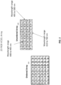
- FIG. 1 illustrates example embodiments of the disclosure comprising 2D RGB VCSEL arrays, in accordance with various example implementations of this disclosure.
- discrete VCSELs are used in each wavelength range and are mounted together on a chip to form a 1D or a 2D array.
- GaN-based VCSELs with an InGaN active region may be used with dielectric mirrors for the blue and green ranges.
- VCSELs with an (AIGa)lnP active region and an AlGaAs N and P Distributed Bragg Reflector (DBR) mirror stacks grown on a GaAs substrate may be used for red range.
- DBR Distributed Bragg Reflector
- the arrays can be ordered 101 or unordered 103.
- the composite arrays can be addressable by row, by column or at individual VCSEL level.
- the arrays 101, 103 may be biased in a common cathode or a common anode configuration.
- the arrays 101, 103 may have additional VCSEL attributes and process elements.
- the VCSEL arrays 101, 103 may use a laser transfer process.
- Laser-Induced Forward Transfer (LIFT) and pixel/repair trimming may be used to reduce the cost of constructing an RGB VCSEL array 101, 103.
- LIFT Laser-Induced Forward Transfer
- pixel/repair trimming may be used to reduce the cost of constructing an RGB VCSEL array 101, 103.
- Pulsed Laser Deposition is the deposition of reflective layers and may be used for a resonant cavity LED.
- PLD is a thin-film deposition technique using high-energy laser pulses to vaporize the surface of a solid target inside a vacuum chamber. The vapor is then condensed on a substrate to form a thin film of up to a few micrometers in thickness.
- a thin film of a reflecting material can be used as a mirror in a blue or green LED. While the reflectivity may not be not high enough to use it in a VCSEL structure, it may be used in a Resonant Cavity (RC) LED. This can simplify and reduce the cost of the blue and green light source in some applications that utilize RC LEDs instead of VCSELs.
- RC Resonant Cavity
- FIGs. 3a-c illustrate example embodiments of the disclosure comprising active regions 305 between DBR mirror stacks 303 and 307, in accordance with various example implementations of this disclosure.
- the optical properties of the layers in an AR glass may reach maximum efficiency for polarized light.
- a grating layer 301 can be defined in the cap layer of the light emitting side.
- FIG. 3a shows how this solution can be used for top emitting devices.
- FIG. 3b shows how this solution can be used for bottom emitting devices.
- the gratings 301 can be lithographically defined.
- the pitch and the duty cycle can be optimized for a maximum polarization extinction ratio.
- Open-dirac electromagnetic cavities with linear dispersion may be realized by a truncated photonic crystal arranged in a hexagonal pattern. Such open-dirac electromagnetic cavities may exhibit unconventional scaling of losses in reciprocal space, leading to single-mode lasing that is maintained as the cavity is scaled up in size.
- VCSELs may be developed based on the principle of the open-Dirac electromagnetic cavities with linear dispersion. These VCSELs may be current injected and may work in the RGB range.
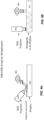
- an RGB projector 401 may be aimed at a reflective element 407 on AR glass 403 before being viewed 405. As shown in FIG. 4b , an RGB projector 401 may also be aimed at a waveguide in an AR glass 403 before being viewed 405.
- Another implementation may comprise a non-transitory machine-readable (e.g., computer readable) medium (e.g., FLASH drive, optical disk, magnetic storage disk, or the like) having stored thereon one or more lines of code that, when executed by a machine, cause the machine to be configured (e.g., to load software and/or firmware into its circuits) to operate as a system described in this disclosure.
- a machine-readable medium e.g., FLASH drive, optical disk, magnetic storage disk, or the like
- x, y, and/or z means any element of the seven-element set ⁇ (x), (y), (z), (x, y), (x, z), (y, z), (x, y, z) ⁇ .
- exemplary means serving as a non-limiting example, instance, or illustration.
- e.g. and “for example” set off lists of one or more non-limiting examples, instances, or illustrations.
Landscapes
- Physics & Mathematics (AREA)
- Condensed Matter Physics & Semiconductors (AREA)
- General Physics & Mathematics (AREA)
- Electromagnetism (AREA)
- Optics & Photonics (AREA)
- Semiconductor Lasers (AREA)
Abstract
Description
- This application claims the benefit of and priority to
U.S. Provisional Patent Application Ser. No. 63/433,147, titled RED-GREEN-BLUE, VERTICAL-CAVITY, SURFACE-EMITTING LASER ARRAY, filed Dec. 16, 2022 - Limitations and disadvantages of VCSEL arrays will become apparent to one of skill in the art, through comparison of such approaches with some aspects of the present method and system set forth in the remainder of this disclosure with reference to the drawings.
- Systems and methods are provided for producing an RGB VCSEL array, substantially as illustrated by and/or described in connection with at least one of the figures, as set forth more completely in the claims.
-
-
FIG. 1 illustrates example embodiments of the disclosure comprising 2D RGB VCSEL arrays, in accordance with various example implementations of this disclosure. -
FIG. 2 illustrates an example embodiment of the disclosure comprising active regions and tunnel junctions between Distributed Bragg Reflector (DBR) mirror stacks, in accordance with various example implementations of this disclosure. -
FIGs. 3a-c illustrate example embodiments of the disclosure comprising active regions between DBR mirror stacks, in accordance with various example implementations of this disclosure. -
FIGs. 4a-b illustrate example embodiments of the disclosure comprising RGB VCSEL arrays for an AR application, in accordance with various example implementations of this disclosure. -
FIGs. 5 and 6 illustrate example embodiments of micro optics on a wafer, in accordance with various example implementations of this disclosure. -
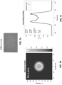
FIGs. 7a-c illustrates an example embodiment of the disclosure comprising a VCSEL without a lens, in accordance with various example implementations of this disclosure. -
FIGs. 8a-c illustrates an example embodiment of the disclosure comprising a VCSEL with a collimator, in accordance with various example implementations of this disclosure. -
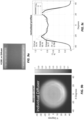
FIGs. 9a-c illustrates an example embodiment of the disclosure comprising a VCSEL with a diffuser, in accordance with various example implementations of this disclosure. - This disclosure describes a composite array of vertical-cavity surface-emitting lasers (VCSELs), including discrete VCSELs emitting at one wavelength of a group of wavelengths greater than two, each wavelength of said group of wavelengths being in the blue range (i.e., 440 to 495 nm), the green range (i.e., 495 to 580 nm) or the red range (i.e., 610 to 760 nm).
-
FIG. 1 illustrates example embodiments of the disclosure comprising 2D RGB VCSEL arrays, in accordance with various example implementations of this disclosure. - As an example of the implementation, discrete VCSELs are used in each wavelength range and are mounted together on a chip to form a 1D or a 2D array. GaN-based VCSELs with an InGaN active region may be used with dielectric mirrors for the blue and green ranges. VCSELs with an (AIGa)lnP active region and an AlGaAs N and P Distributed Bragg Reflector (DBR) mirror stacks grown on a GaAs substrate may be used for red range.
- The arrays can be ordered 101 or unordered 103. The composite arrays can be addressable by row, by column or at individual VCSEL level. The
arrays - The
arrays arrays RGB VCSEL array - To overcome the surface recombination on the chip sidewalls in micro-LED and micro-VCSEL, the contour of the chip may be implanted from top side through all epi layers remaining on the chip after laser transfer.
- The blue and green GaN-based VCSEL structures may comprise dielectric DBR mirrors. The light generating section (active region) of the VCSEL may be grown by epitaxy. A wafer bonding process or wafer fusion may be used to combine the DBR stack with the active region. Fusion bonding refers to spontaneous adhesion of two planar substrates without the addition of any intermediate layer. As an alternative approach, DBRs of appropriate design may be placed individually for each emitter of each wavelength using a two-step laser transfer process, where the first step is DBR and the second step is for the active region. Because the dielectric DBR is an insulator, intracavity contacts are used to inject current into the active region.
- Pulsed Laser Deposition (PLD) is the deposition of reflective layers and may be used for a resonant cavity LED. PLD is a thin-film deposition technique using high-energy laser pulses to vaporize the surface of a solid target inside a vacuum chamber. The vapor is then condensed on a substrate to form a thin film of up to a few micrometers in thickness. A thin film of a reflecting material can be used as a mirror in a blue or green LED. While the reflectivity may not be not high enough to use it in a VCSEL structure, it may be used in a Resonant Cavity (RC) LED. This can simplify and reduce the cost of the blue and green light source in some applications that utilize RC LEDs instead of VCSELs.
-
FIG. 2 illustrates an example embodiment of the disclosure comprisingactive regions 205 andtunnel junctions 207 betweenDBR mirror stacks - This multi-junction VCSEL technology implements multiple
active regions 205 andtunnel junctions 207 between the twoDBR mirror stacks active regions 205 andtunnel junctions 207 increases the power and slope efficiency and, at the same time, results in a higher voltage. - In the context of RGB VCSELs, the efficiency of blue color lasers is typically lower due to the material properties constraints. The blue laser efficiency can be improved by using this multi junction technology. The higher efficiency lasers (i.e., red) may use a standard single junction. This may allow the use of the same current supply with a comparable output power for the three RGB VCSELs.
- Lithographically-defined apertures may provide an alternative to oxide apertures. The oxide-free VCSEL structures may use a lithographically-defined intra-cavity mesa for current and mode confinement. The confinement properties of such intra-cavity mesas are comparable to the oxide apertures, with a higher precision control of the aperture size.
- In another version, the aperture may be controlled by a combination of a tunnel junction and a p-n junction. The p-n junction may be reverse biased thus blocking the current flow. The VCSEL aperture may be determined by the lateral dimension of the tunnel junction. By having the lithographic precision, the modal content of the devices may be accurately controlled in the production flow. For example, AR applications may use narrow linewidths that are produced via such precise modal control.
-
FIGs. 3a-c illustrate example embodiments of the disclosure comprisingactive regions 305 betweenDBR mirror stacks grating layer 301 can be defined in the cap layer of the light emitting side.FIG. 3a shows how this solution can be used for top emitting devices.FIG. 3b shows how this solution can be used for bottom emitting devices. Thegratings 301 can be lithographically defined. The pitch and the duty cycle can be optimized for a maximum polarization extinction ratio. - The solution in
FIG. 3c can be used for either top or bottom emitting devices. Theintra-cavity grating 301 inFIG. 3c also allows back-side emitting VCSELs with polarization locking and optics on the substrate (e.g., bottom emitting). - If additional optical functionality (e.g., a lens, a diffuser, etc.) is added to the emitting side of the VCSEL, the polarization lock can be implemented within the VCSEL cavity. The
grating layer 301 is then etched inside of the cavity as shown inFIG. 3c . This structure can be realized by using wafer bonding or regrowth techniques. - Open-dirac electromagnetic cavities with linear dispersion may be realized by a truncated photonic crystal arranged in a hexagonal pattern. Such open-dirac electromagnetic cavities may exhibit unconventional scaling of losses in reciprocal space, leading to single-mode lasing that is maintained as the cavity is scaled up in size. VCSELs may be developed based on the principle of the open-Dirac electromagnetic cavities with linear dispersion. These VCSELs may be current injected and may work in the RGB range.
-
FIGs. 4a-b illustrate example embodiments of the disclosure comprising RGB VCSEL arrays for an AR application, in accordance with various example implementations of this disclosure. The ability to extend a single mode operation to larger apertures may be very advantageous for AR applications. - As shown in
FIG. 4a , anRGB projector 401 may be aimed at areflective element 407 onAR glass 403 before being viewed 405. As shown inFIG. 4b , anRGB projector 401 may also be aimed at a waveguide in anAR glass 403 before being viewed 405. -
FIGs. 5 and 6 illustrate example embodiments of micro optics on a wafer, in accordance with various example implementations of this disclosure. Micro optics elements could be integrated on top of VCSEL emitters using a wafer level process based on nano imprint lithography (NIL) of a polymer layer dispensed over the VCSEL wafer. Using NIL processes, micro optics elements with high conformance accuracy may be generated with positional accuracy of <1 um. The NIL technology provides the flexibility to produce a variety of micro lenses with different designs, forms and shapes. -
FIGs. 7a-c illustrates an example embodiment of the disclosure comprising a VCSEL without a lens, in accordance with various example implementations of this disclosure.FIG. 7a shows the physical VCSEL.FIG. 7b shows the far field of this VCSEL without a lens.FIG. 7c shows that the far field of the VCSEL without a lens is around 30°. - Two examples of micro optics elements are a collimator and a diffuser.
FIGs. 8a-c illustrates an example embodiment of the disclosure comprising a VCSEL with a collimator, in accordance with various example implementations of this disclosure.FIG. 8a shows the physical VCSEL with the collimator.FIG. 8b shows the far field of this VCSEL with the collimator.FIG. 8c shows that this collimator can collimate the far field of the VCSEL (from around 30° as shown inFIG. 7c ) to below 10°. -
FIGs. 9a-c illustrates an example embodiment of the disclosure comprising a VCSEL with a diffuser, in accordance with various example implementations of this disclosure.FIG. 9a shows the physical VCSEL with the diffuser.FIG. 9b shows the far field of this VCSEL with the diffuser.FIG. 9c shows that this diffuser can expand the far field of the VCSEL (from around 30° as shown inFIG. 7c ) to over 65°. - The present method and/or system may be realized in hardware, software, or a combination of hardware and software. The present methods and/or systems may be realized in a centralized fashion in at least one computing system, or in a distributed fashion where different elements are spread across several interconnected computing systems. Any kind of computing system or other apparatus adapted for carrying out the methods described herein is suited. A typical implementation may comprise one or more application specific integrated circuit (ASIC), one or more field programmable gate array (FPGA), and/or one or more processor (e.g., x86, x64, ARM, PIC, and/or any other suitable processor architecture) and associated supporting circuitry (e.g., storage, DRAM, FLASH, bus interface circuits, etc.). Each discrete ASIC, FPGA, Processor, or other circuit may be referred to as "chip," and multiple such circuits may be referred to as a "chipset." Another implementation may comprise a non-transitory machine-readable (e.g., computer readable) medium (e.g., FLASH drive, optical disk, magnetic storage disk, or the like) having stored thereon one or more lines of code that, when executed by a machine, cause the machine to perform processes as described in this disclosure. Another implementation may comprise a non-transitory machine-readable (e.g., computer readable) medium (e.g., FLASH drive, optical disk, magnetic storage disk, or the like) having stored thereon one or more lines of code that, when executed by a machine, cause the machine to be configured (e.g., to load software and/or firmware into its circuits) to operate as a system described in this disclosure.
- As used herein the terms "circuits" and "circuitry" refer to physical electronic components (i.e. hardware) and any software and/or firmware ("code") which may configure the hardware, be executed by the hardware, and or otherwise be associated with the hardware. As used herein, for example, a particular processor and memory may comprise a first "circuit" when executing a first one or more lines of code and may comprise a second "circuit" when executing a second one or more lines of code. As used herein, "and/or" means any one or more of the items in the list joined by "and/or". As an example, "x and/or y" means any element of the three-element set {(x), (y), (x, y)}. As another example, "x, y, and/or z" means any element of the seven-element set {(x), (y), (z), (x, y), (x, z), (y, z), (x, y, z)}. As used herein, the term "exemplary" means serving as a non-limiting example, instance, or illustration. As used herein, the terms "e.g.," and "for example" set off lists of one or more non-limiting examples, instances, or illustrations. As used herein, circuitry is "operable" to perform a function whenever the circuitry comprises the necessary hardware and code (if any is necessary) to perform the function, regardless of whether performance of the function is disabled or not enabled (e.g., by a user-configurable setting, factory trim, etc.). As used herein, the term "based on" means "based at least in part on." For example, "x based on y" means that "x" is based at least in part on "y" (and may also be based on z, for example).
- While the present method and/or system has been described with reference to certain implementations, it will be understood by those skilled in the art that various changes may be made and equivalents may be substituted without departing from the scope of the present method and/or system. In addition, many modifications may be made to adapt a particular situation or material to the teachings of the present disclosure without departing from its scope. Therefore, it is intended that the present method and/or system not be limited to the particular implementations disclosed, but that the present method and/or system will include all implementations falling within the scope of the appended claims.
Claims (20)
- A system, the system comprising:
an array of vertical-cavity surface-emitting lasers (VCSELs), wherein:
the array of VCSELs comprises:at least one VCSEL operable to emit in a blue wavelength range,at least one VCSEL operable to emit in a green wavelength range, andat least one VCSEL operable to emit in a red wavelength range; and each VCSEL in the array of VCSELs comprises:an active region, andtwo distributed Bragg reflectors. - The system of claim 1, wherein the blue wavelength range is 440 to 495 nm, the green wavelength range is 495 to 580 nm and blue wavelength range is 610 to 760 nm.
- The system of claim 1, wherein the array of VCSELs is a one-dimensional array.
- The system of claim 1, wherein the array of VCSELs is a two-dimensional array.
- The system of claim 1, wherein the at least one VCSEL operable to emit in the blue wavelength range is GaN-based and comprises an InGaN active region.
- The system of claim 1, wherein the at least one VCSEL operable to emit in the green wavelength range is GaN-based and comprises an InGaN active region.
- The system of claim 1, wherein the at least one VCSEL operable to emit in the red wavelength range comprises an (AIGa)lnP active region and AlGaAs N and P Distributed Bragg Reflector (DBR) mirror stacks grown on a GaAs substrate.
- The system of claim 1, wherein at least one VCSEL, of the array of VCSELs, comprises a plurality of active regions between the two DBR mirror stacks.
- The system of claim 8, wherein each active region, of the plurality of active regions, is separated from each other active region, of the plurality of active regions, by a tunnel junction.
- The system of claim 8, wherein the at least one VCSEL that comprises the plurality of active regions between the two DBR mirror stacks is operable to emit in the blue wavelength range.
- The system of claim 10, wherein the at least one VCSEL that is operable to emit in the red wavelength range comprises a single active region between the two DBR mirror stacks.
- The system of claim 11, wherein the at least one VCSEL that is operable to emit in the blue wavelength range and the at least one VCSEL that is operable to emit in the red wavelength range are operably powered by a common current supply.
- The system of claim 1, wherein each VCSEL of the array of VCSELs comprises a grating in a cap layer of a light emitting side.
- The system of claim 1, wherein each VCSEL of the array of VCSELs comprises a grating adjacent to an active region.
- The system of claim 14, wherein the grating is etched inside of a cavity.
- The system of claim 1, wherein each VCSEL of the array of VCSELs comprises an open-Dirac electromagnetic cavity with linear dispersion.
- The system of claim 1, wherein each VCSEL of the array of VCSELs comprises a micro lens.
- The system of claim 17, wherein the micro lens is a collimator.
- The system of claim 17, wherein the micro lens is a diffuser.
- The system of claim 17, wherein the micro lens is integrated on top of each VCSEL via nano imprint lithography (NIL) of a polymer layer.
Applications Claiming Priority (2)
| Application Number | Priority Date | Filing Date | Title |
|---|---|---|---|
| US202263433147P | 2022-12-16 | 2022-12-16 | |
| US18/530,296 US20240204486A1 (en) | 2022-12-16 | 2023-12-06 | Red-green-blue, vertical-cavity, surface-emitting laser array |
Publications (2)
| Publication Number | Publication Date |
|---|---|
| EP4398429A2 true EP4398429A2 (en) | 2024-07-10 |
| EP4398429A3 EP4398429A3 (en) | 2024-09-04 |
Family
ID=89223306
Family Applications (1)
| Application Number | Title | Priority Date | Filing Date |
|---|---|---|---|
| EP23217092.8A Pending EP4398429A3 (en) | 2022-12-16 | 2023-12-15 | Red-green-blue, vertical-cavity, surface-emitting laser array |
Country Status (4)
| Country | Link |
|---|---|
| US (1) | US20240204486A1 (en) |
| EP (1) | EP4398429A3 (en) |
| JP (2) | JP7744963B2 (en) |
| KR (1) | KR20240095074A (en) |
Families Citing this family (1)
| Publication number | Priority date | Publication date | Assignee | Title |
|---|---|---|---|---|
| WO2026057372A1 (en) * | 2024-09-16 | 2026-03-19 | Ams-Osram International Gmbh | Laser devices and methods for producing thereof |
Family Cites Families (19)
| Publication number | Priority date | Publication date | Assignee | Title |
|---|---|---|---|---|
| US5325386A (en) * | 1992-04-21 | 1994-06-28 | Bandgap Technology Corporation | Vertical-cavity surface emitting laser assay display system |
| JP2001257424A (en) * | 2000-03-13 | 2001-09-21 | Toshiba Corp | Vertical cavity surface emitting device |
| US6822991B2 (en) * | 2002-09-30 | 2004-11-23 | Lumileds Lighting U.S., Llc | Light emitting devices including tunnel junctions |
| JP2007234824A (en) * | 2006-02-28 | 2007-09-13 | Canon Inc | Vertical cavity surface emitting laser |
| WO2011093885A1 (en) * | 2010-01-29 | 2011-08-04 | Hewlett-Packard Development Company L.P. | Vertical-cavity surface-emitting lasers with non-periodic gratings |
| JP5765892B2 (en) * | 2010-05-27 | 2015-08-19 | キヤノン株式会社 | Vertical cavity surface emitting laser and image forming apparatus using the same |
| JP6152848B2 (en) * | 2012-07-06 | 2017-06-28 | パナソニックIpマネジメント株式会社 | Semiconductor light emitting device |
| US10256609B2 (en) * | 2015-09-15 | 2019-04-09 | Sony Corporation | Surface light-emitting laser |
| JP2016054314A (en) * | 2015-12-01 | 2016-04-14 | ヒューレット−パッカード デベロップメント カンパニー エル.ピー.Hewlett‐Packard Development Company, L.P. | Multimode monolithic vertical cavity surface emitting laser array and laser system including the same |
| CN109906518B (en) * | 2016-12-05 | 2022-07-01 | 歌尔股份有限公司 | Micro laser diode transfer method and micro laser diode display device manufacturing method |
| US20200006924A1 (en) * | 2016-12-05 | 2020-01-02 | Goertek, Inc. | Micro Laser Diode Display Device and Electronics Apparatus |
| EP3588700A1 (en) * | 2018-06-26 | 2020-01-01 | Koninklijke Philips N.V. | Vcsel device for an smi sensor for recording three-dimensional pictures |
| JP7288360B2 (en) * | 2019-07-01 | 2023-06-07 | スタンレー電気株式会社 | Vertical cavity light emitting device |
| KR102899575B1 (en) * | 2020-03-27 | 2025-12-15 | 엘지전자 주식회사 | Image acquiring device |
| EP4143933A4 (en) * | 2020-04-27 | 2024-05-29 | Technion Research & Development Foundation Ltd. | Topologic insulator surface emitting laser system |
| CN114520461B (en) * | 2020-11-18 | 2023-03-28 | 浙江睿熙科技有限公司 | VCSEL laser with multiple tunnel junctions and preparation method thereof |
| US20240275132A1 (en) * | 2021-05-31 | 2024-08-15 | Kyocera Corporation | Semiconductor device, method and apparatus for manufacturing semiconductor device, and electronic device |
| JP7853546B2 (en) * | 2021-08-02 | 2026-04-30 | 日亜化学工業株式会社 | light source device |
| WO2023181716A1 (en) * | 2022-03-24 | 2023-09-28 | ソニーグループ株式会社 | Surface-emitting laser, surface-emitting laser array, and electronic device |
-
2023
- 2023-12-06 US US18/530,296 patent/US20240204486A1/en active Pending
- 2023-12-15 JP JP2023212199A patent/JP7744963B2/en active Active
- 2023-12-15 EP EP23217092.8A patent/EP4398429A3/en active Pending
- 2023-12-18 KR KR1020230184613A patent/KR20240095074A/en active Pending
-
2025
- 2025-09-12 JP JP2025152034A patent/JP2025172971A/en active Pending
Also Published As
| Publication number | Publication date |
|---|---|
| US20240204486A1 (en) | 2024-06-20 |
| JP2024086696A (en) | 2024-06-27 |
| EP4398429A3 (en) | 2024-09-04 |
| KR20240095074A (en) | 2024-06-25 |
| JP2025172971A (en) | 2025-11-26 |
| JP7744963B2 (en) | 2025-09-26 |
Similar Documents
| Publication | Publication Date | Title |
|---|---|---|
| US11482835B2 (en) | VCSEL device with multiple stacked active regions | |
| CN111149226B (en) | Single chip series connection VCSEL array | |
| RU2623663C2 (en) | Surface-emitting laser device with vertical external resonator with optical pumping | |
| CN112531463B (en) | Combining light-emitting elements of different divergences on the same substrate | |
| US12237648B2 (en) | Bi-directional vertical cavity surface emitting lasers | |
| US6097041A (en) | Light-emitting diode with anti-reflector | |
| US20200119527A1 (en) | Emitter array with multiple groups of interspersed emitters | |
| US20230006421A1 (en) | Vertical cavity surface emitting laser element, vertical cavity surface emitting laser element array, vertical cavity surface emitting laser module, and method of producing vertical cavity surface emitting laser element | |
| WO2020247291A1 (en) | Vertical-cavity surface-emitting laser using dichroic reflectors | |
| CN115275776A (en) | Method of incorporating a control structure within a vertical cavity surface emitting laser device cavity | |
| JP2025172971A (en) | Red-green-blue vertical cavity surface-emitting laser array | |
| US20260074487A1 (en) | Vertical cavity surface emitting laser and method for producing same | |
| US12046876B2 (en) | Vertically offset vertical cavity surface emitting lasers | |
| Feezell | Status and future of GaN-based vertical-cavity surface-emitting lasers | |
| CN115566533A (en) | A multi-chip addressable laser | |
| TW202236766A (en) | Bottom-emitting emitter array with a bottom side metal layer | |
| US11901701B2 (en) | Surface emitting laser element, surface emitting laser, surface emitting laser device, light source device, and detection apparatus | |
| US10666020B2 (en) | Reconfigurable emitter array | |
| CN118213858A (en) | Red-green-blue vertical cavity surface emitting laser array | |
| CN117748291A (en) | Vertical cavity surface emitting laser and manufacturing method thereof | |
| JP2025086542A (en) | Light source device and distance measuring device | |
| CN113991424B (en) | A high-power single-side light emitting semiconductor laser based on tilted surface grating | |
| Gębski et al. | First vertical-cavity surface-emitting laser made entirely in Poland | |
| US20250007247A1 (en) | Vertical cavity surface emitting laser device with dual wavelength bands | |
| US20230238779A1 (en) | Dot-projecting optical device |
Legal Events
| Date | Code | Title | Description |
|---|---|---|---|
| PUAI | Public reference made under article 153(3) epc to a published international application that has entered the european phase |
Free format text: ORIGINAL CODE: 0009012 |
|
| STAA | Information on the status of an ep patent application or granted ep patent |
Free format text: STATUS: REQUEST FOR EXAMINATION WAS MADE |
|
| 17P | Request for examination filed |
Effective date: 20231215 |
|
| AK | Designated contracting states |
Kind code of ref document: A2 Designated state(s): AL AT BE BG CH CY CZ DE DK EE ES FI FR GB GR HR HU IE IS IT LI LT LU LV MC ME MK MT NL NO PL PT RO RS SE SI SK SM TR |
|
| PUAL | Search report despatched |
Free format text: ORIGINAL CODE: 0009013 |
|
| P01 | Opt-out of the competence of the unified patent court (upc) registered |
Free format text: CASE NUMBER: APP_42619/2024 Effective date: 20240719 |
|
| AK | Designated contracting states |
Kind code of ref document: A3 Designated state(s): AL AT BE BG CH CY CZ DE DK EE ES FI FR GB GR HR HU IE IS IT LI LT LU LV MC ME MK MT NL NO PL PT RO RS SE SI SK SM TR |
|
| RIC1 | Information provided on ipc code assigned before grant |
Ipc: H01S 5/40 20060101ALI20240801BHEP Ipc: H01S 5/183 20060101ALI20240801BHEP Ipc: H01S 5/065 20060101ALI20240801BHEP Ipc: H01S 5/42 20060101ALI20240801BHEP Ipc: H01S 5/30 20060101AFI20240801BHEP |
|
| GRAP | Despatch of communication of intention to grant a patent |
Free format text: ORIGINAL CODE: EPIDOSNIGR1 |
|
| STAA | Information on the status of an ep patent application or granted ep patent |
Free format text: STATUS: GRANT OF PATENT IS INTENDED |
|
| INTG | Intention to grant announced |
Effective date: 20251219 |
|
| GRAJ | Information related to disapproval of communication of intention to grant by the applicant or resumption of examination proceedings by the epo deleted |
Free format text: ORIGINAL CODE: EPIDOSDIGR1 |
|
| STAA | Information on the status of an ep patent application or granted ep patent |
Free format text: STATUS: REQUEST FOR EXAMINATION WAS MADE |
|
| GRAP | Despatch of communication of intention to grant a patent |
Free format text: ORIGINAL CODE: EPIDOSNIGR1 |
|
| STAA | Information on the status of an ep patent application or granted ep patent |
Free format text: STATUS: GRANT OF PATENT IS INTENDED |
|
| INTG | Intention to grant announced |
Effective date: 20260428 |