EP4398284A1 - Display panel and display device - Google Patents
Display panel and display device Download PDFInfo
- Publication number
- EP4398284A1 EP4398284A1 EP21839808.9A EP21839808A EP4398284A1 EP 4398284 A1 EP4398284 A1 EP 4398284A1 EP 21839808 A EP21839808 A EP 21839808A EP 4398284 A1 EP4398284 A1 EP 4398284A1
- Authority
- EP
- European Patent Office
- Prior art keywords
- display panel
- expansion portion
- light
- corner
- openings
- Prior art date
- Legal status (The legal status is an assumption and is not a legal conclusion. Google has not performed a legal analysis and makes no representation as to the accuracy of the status listed.)
- Pending
Links
Images




Classifications
-
- H—ELECTRICITY
- H10—SEMICONDUCTOR DEVICES; ELECTRIC SOLID-STATE DEVICES NOT OTHERWISE PROVIDED FOR
- H10K—ORGANIC ELECTRIC SOLID-STATE DEVICES
- H10K50/00—Organic light-emitting devices
- H10K50/80—Constructional details
- H10K50/85—Arrangements for extracting light from the devices
- H10K50/858—Arrangements for extracting light from the devices comprising refractive means, e.g. lenses
-
- H—ELECTRICITY
- H10—SEMICONDUCTOR DEVICES; ELECTRIC SOLID-STATE DEVICES NOT OTHERWISE PROVIDED FOR
- H10K—ORGANIC ELECTRIC SOLID-STATE DEVICES
- H10K59/00—Integrated devices, or assemblies of multiple devices, comprising at least one organic light-emitting element covered by group H10K50/00
- H10K59/80—Constructional details
- H10K59/875—Arrangements for extracting light from the devices
- H10K59/879—Arrangements for extracting light from the devices comprising refractive means, e.g. lenses
-
- G—PHYSICS
- G02—OPTICS
- G02B—OPTICAL ELEMENTS, SYSTEMS OR APPARATUS
- G02B3/00—Simple or compound lenses
- G02B3/0006—Arrays
-
- H—ELECTRICITY
- H10—SEMICONDUCTOR DEVICES; ELECTRIC SOLID-STATE DEVICES NOT OTHERWISE PROVIDED FOR
- H10K—ORGANIC ELECTRIC SOLID-STATE DEVICES
- H10K59/00—Integrated devices, or assemblies of multiple devices, comprising at least one organic light-emitting element covered by group H10K50/00
- H10K59/10—OLED displays
- H10K59/12—Active-matrix OLED [AMOLED] displays
-
- H—ELECTRICITY
- H10—SEMICONDUCTOR DEVICES; ELECTRIC SOLID-STATE DEVICES NOT OTHERWISE PROVIDED FOR
- H10K—ORGANIC ELECTRIC SOLID-STATE DEVICES
- H10K59/00—Integrated devices, or assemblies of multiple devices, comprising at least one organic light-emitting element covered by group H10K50/00
- H10K59/10—OLED displays
- H10K59/12—Active-matrix OLED [AMOLED] displays
- H10K59/1201—Manufacture or treatment
-
- H—ELECTRICITY
- H10—SEMICONDUCTOR DEVICES; ELECTRIC SOLID-STATE DEVICES NOT OTHERWISE PROVIDED FOR
- H10K—ORGANIC ELECTRIC SOLID-STATE DEVICES
- H10K59/00—Integrated devices, or assemblies of multiple devices, comprising at least one organic light-emitting element covered by group H10K50/00
- H10K59/30—Devices specially adapted for multicolour light emission
- H10K59/35—Devices specially adapted for multicolour light emission comprising red-green-blue [RGB] subpixels
-
- H—ELECTRICITY
- H10—SEMICONDUCTOR DEVICES; ELECTRIC SOLID-STATE DEVICES NOT OTHERWISE PROVIDED FOR
- H10K—ORGANIC ELECTRIC SOLID-STATE DEVICES
- H10K59/00—Integrated devices, or assemblies of multiple devices, comprising at least one organic light-emitting element covered by group H10K50/00
- H10K59/80—Constructional details
- H10K59/87—Passivation; Containers; Encapsulations
- H10K59/873—Encapsulations
Definitions
- a ratio of an area of the expansion portion to an area of the main body portion is less than or equal to 0.2.
- the expansion portion surrounds the first corner and the second corner.
- an angle between the side surface of the micro lenses and the plane where the array substrate is located is a first angle; wherein on a cross-section perpendicular to the two opposite expansion portions, an angle between the side surface of the micro lenses and the plane where the array substrate is located is a second angle; and wherein, a range of a difference between the first angle and the second angle is less than 20 degrees.
- the first angle and the second angle are equal.
- FIG 1 is a schematic cross-sectional structure diagram of a display panel provided by an embodiment of the present disclosure.
- An embodiment of the present disclosure provides a display panel 1, which includes an array substrate 11, a plurality of light-emitting pixel units 12, a micro lens layer 14, and a passivation layer 15.
- a pattern shape of the light-emitting pixel unit 12 has corners, correspondingly, the pattern shape of a mask used to form the opening also has corners, and the corners are formed by an intersection of two adjacent side edges. Since an ultraviolet light used in an exposure process will be diffracted at the two adjacent side edges forming the corners, the ultraviolet light bypasses the edges of the two adjacent side edges and spreads to different degrees. Because a relative distance between the two adjacent side edges at the corners is relatively short, the ultraviolet light diffracted from the two adjacent side edges into the mask is superimposed at the corner, resulting in greater intensity of the diffracted light. As a result, the taper angle ⁇ of the etched micro lenses 141 is low and extends inward, which affects the light convergence effect of the micro lenses 141.
- the term of "surround" in this embodiment means that a ray formed by taking a vertex of the first corner 2112a as an end point to extend in any direction away from the main body portion 211 passes through the first sub-expansion portion 212a, and a ray formed by taking a vertex of the second corner 2112b as an end point and extending in any direction away from the main body portion 211 passes through the second sub-expansion portion 212b.
- a sum of areas of the first sub-expansion portion 212a and the second sub-expansion portion 212b in FIG 2C is smaller than that of the expansion portion in FIG 2A . It is beneficial to reduce the difference between the formed first openings 142 and the corresponding light-emitting pixel units 12, thereby further improving the light condensing effect of the micro lenses 141.
- a ratio of the area of the expansion portion 212 to the area of the main body portion 211 is less than or equal to 0.2.
- an angle between a side surface of the micro lenses 141 and a plane where the array substrate 11 is located ranges from 50 degrees to 90 degrees.
- FIG 3A is a cross-sectional view along A-A in FIG 2A .
- FIG 3B is a cross-sectional view along B-B in FIG 2A .
- a range of the difference between the first angle ⁇ 1 and the second angle ⁇ 2 is less than 20 degrees.
- the shape of the main body 211 is a pearl shape.
- the main body 211 may also have other shapes, which is not limited in the present disclosure.
- the embodiment of the present disclosure takes the shape of the main body portion 211 as a pearl as an example for explanation.
- FIG 4A is a schematic diagram of a planar structure of a micro lens layer of a display panel according to an embodiment of the present disclosure.
- FIG 4B is a schematic diagram of the arrangement of light-emitting pixel units provided by an embodiment of the present disclosure.
- the plurality of light-emitting pixel units 12 at least includes a plurality of red light-emitting pixel units 121, a plurality of green light-emitting pixel units 122, and a plurality of blue light-emitting pixel units 123.
- the first openings 142 correspond to the red light-emitting pixel unit 121 and the blue light-emitting pixel unit 123.
- the light-emitting area of the red light-emitting pixel unit 121 is larger than the light-emitting area of the green light-emitting pixel unit 122. Therefore, in a plane direction of the display panel 1, the area of the first opening 142 corresponding to the red light-emitting pixel unit 121 is larger than the area of the first opening 142 corresponding to the green light-emitting pixel unit 122.
- the display panel 1 further includes a plurality of second openings 143.
- the second opening 143 is arranged corresponding to the green light-emitting pixel unit 122.
- the pattern shape of the second opening 143 is the same as the pattern shape of the green light-emitting pixel unit 122.
- the light-emitting area of the green light-emitting pixel unit 122 is smaller than the light-emitting area of the red light-emitting pixel unit 121 and the blue light-emitting pixel unit 123. Therefore, in the plane direction of the display panel 1, the area of the second opening 143 is smaller than the area of the first opening 142.
- the shape of the second opening 143 in the embodiment of the present disclosure is arc-shaped, there is no corner 2112 of the main body portion 211 in the first opening 142. Therefore, the second opening 143 does not need to be provided with the expansion portion 212.
- the display panel 1 further includes an encapsulation layer 13 arranged between the light-emitting pixel unit 12 and the micro lens layer 14.
- the encapsulation layer 13 covers the light-emitting pixel units 12 and the array substrate 11.
- the micro lens layer 14 is provided on a side of the encapsulation layer 13 away from the array substrate 11.
- a substrate is provided.
- a plurality of thin film transistors and a plurality of signal traces are formed on the substrate.
- the thin film transistor includes a gate, a gate insulating layer, an active layer, a source and drain metal layer, and other film layers, all of which are sequentially formed on the substrate. Since this is a prior art, it will not be described in detail here.
Landscapes
- Physics & Mathematics (AREA)
- Engineering & Computer Science (AREA)
- Optics & Photonics (AREA)
- Microelectronics & Electronic Packaging (AREA)
- General Physics & Mathematics (AREA)
- Manufacturing & Machinery (AREA)
- Electroluminescent Light Sources (AREA)
- Devices For Indicating Variable Information By Combining Individual Elements (AREA)
Abstract
Description
- The present disclosure relates to displays, and more particularly to a display panel and a display device.
- For an organic light-emitting diode (OLED) display panel, in order to improve a luminous efficiency of the light-emitting device, reduce power consumption and extend a life span, a micro lens structure is used for light extraction. The micro lens structure includes a plurality of micro lenses, and the micro lenses are usually prepared by using a mask with a photolithography pattern. However, an ultraviolet light diffracted into the mask will be stronger when superimposed at corners of a photolithography pattern. As a result, an etched taper angle is greatly reduced and extends inward, which affects a light convergence effect of the micro lens structure.
- An embodiment of the present application provides a display panel and a display device, so as to solve a technical problem that when the micro lens layer of an existing display panel is used, a taper angle that is etched is greatly reduced and extends inward, which affects a light convergence effect of the micro lens structure.
- In order to solve the above problems, technical solutions provided by this application are as follows:
- The present application provides a display panel comprising:
- an array substrate;
- a plurality of light-emitting pixel units arranged on the array substrate;
- a micro lens layer arranged on a side of the light-emitting pixel units away from the array substrate, wherein the micro lens layer comprises a plurality of micro lenses and a plurality of openings, the openings are formed between two adjacent micro lenses, and the openings are arranged corresponding to the light-emitting pixel units;
- a passivation layer covering the micro lens layer, wherein a refractive index of the passivation layer is greater than a refractive index of the micro lens layer; and
- an encapsulation layer covering the light-emitting pixel units and the array substrate,
- wherein the plurality of openings include a plurality of first openings, and in a direction along a plane of the display panel, each of the first openings includes a main body portion and at least one expansion portion, wherein the main body portion includes a plurality of side edges, and a corner is formed at the intersection of two adjacent side edges, wherein the expansion portion is arranged at the corner, and the expansion portion is an arc-shaped convex surface.
- According to a display panel provided by the present application, the plurality of side edges include a plurality of first sides and a plurality of second sides, and the first sides and two adjacent second sides respectively form a first corner and a second corner, wherein the expansion portion is provided at the first corner and the second corner.
- According to a display panel provided by the present application, the expansion portion surrounds the first corner and the second corner.
- According to a display panel provided by the present application, the expansion portion is located between two adjacent extension lines of the first side, and a circle where the expansion portion is located is circumscribed to a circle where the two adjacent first sides are located, respectively.
- According to a display panel provided by the present application, the expansion portion at least comprises a first sub-expansion portion and a second sub-expansion portion connected with each other, wherein the first sub-expansion portion surrounds the first corner, and the second sub-expansion portion surrounds the second corner.
- According to a display panel provided by the present application, a ratio of an area of the expansion portion to an area of the main body portion is less than or equal to 0.2.
- According to a display panel provided by the present application, an angle between a side surface of the micro lenses and a plane where the array substrate is located is in a range of 50 degrees to 90 degrees.
- The present application provides a display panel comprising:
- an array substrate;
- a plurality of light-emitting pixel units arranged on the array substrate;
- a micro lens layer arranged on a side of the light-emitting pixel units away from the array substrate, wherein the micro lens layer comprises a plurality of micro lenses and a plurality of openings, the openings are formed between two adjacent micro lenses, and the openings are arranged corresponding to the light-emitting pixel units; and
- a passivation layer covering the micro lens layer, wherein a refractive index of the passivation layer is greater than a refractive index of the micro lens layer,
- wherein the plurality of openings include a plurality of first openings, and in a direction along a plane of the display panel, each of the first openings includes a main body portion and at least one expansion portion, wherein the main body portion includes a plurality of side edges, and a corner is formed at the intersection of two adjacent side edges, wherein the expansion portion is arranged at the corner, and the expansion portion is an arc-shaped convex surface.
- According to a display panel provided by the present application, the plurality of side edges include a plurality of first sides and a plurality of second sides, and the first sides and two adjacent second sides respectively form a first corner and a second corner, wherein the expansion portion is provided at the first corner and the second corner.
- According to a display panel provided by the present application, the expansion portion surrounds the first corner and the second corner.
- According to a display panel provided by the present application, the expansion portion is located between two adjacent extension lines of the first side, and a circle where the expansion portion is located is circumscribed to a circle where the two adjacent first sides are located, respectively.
- According to a display panel provided by the present application, the expansion portion at least comprises a first sub-expansion portion and a second sub-expansion portion connected with each other, wherein the first sub-expansion portion surrounds the first corner, and the second sub-expansion portion surrounds the second corner.
- According to a display panel provided by the present application, a ratio of an area of the expansion portion to an area of the main body portion is less than or equal to 0.2.
- According to a display panel provided by the present application, an angle between a side surface of the micro lenses and a plane where the array substrate is located is in a range of 50 degrees to 90 degrees.
- According to a display panel provided by the present application, on a cross-section perpendicular to the two opposite first sides, an angle between the side surface of the micro lenses and the plane where the array substrate is located is a first angle; wherein on a cross-section perpendicular to the two opposite expansion portions, an angle between the side surface of the micro lenses and the plane where the array substrate is located is a second angle; and
wherein, a range of a difference between the first angle and the second angle is less than 20 degrees. - According to a display panel provided by the present application, the first angle and the second angle are equal.
- According to a display panel provided by the present application, the plurality of side edges include four first sides and four second sides, wherein the four first sides and the four second sides are alternately connected to form a closed figure, and the first sides are arc lines recessed toward an inside of the closed figure.
- According to a display panel provided by the present application, a planar shape of the main body portion is the same as a planar shape of corresponding light-emitting pixel units.
- According to a display panel provided by the present application, the openings further comprise a second opening, and a planar shape of the second opening is an ellipse or a circle; and the plurality of light-emitting pixel units at least include a red light-emitting pixel unit, a green light-emitting pixel unit, and a blue light-emitting pixel unit, wherein the first openings correspond to the red light-emitting pixel unit and the green light-emitting pixel unit, and the second opening corresponds to the blue light-emitting pixel unit.
- The present application provides a display device including the above-mentioned display panel.
- Beneficial effects of the present application are that: in the display panel and the display device provided in the present application, the display panel includes a micro lens layer and a passivation layer, the micro lens layer includes a plurality of micro lenses and a plurality of openings, and the plurality of openings includes a plurality of first openings, where each of the first openings includes a main body. In the present application, by setting an expansion portion at the corner to fine-tune a shape of the first opening based on a pattern of the main body portion. In one aspect, the first openings are made to be close to the light-emitting pixel unit in shape, so as to avoid reducing a light condensing effect of the micro lenses due to a large difference between the shape of the first openings and the light-emitting pixel units. In another aspect, forming a flared portion at the corner of the main body portion increases a distance between adjacent side edges, which can reduce a superimposed intensity of a diffracted light diffused into a mask at the corner, thereby improving the taper angle of the micro lenses. It is beneficial to improve a light condensing effect of the micro lenses, thereby improving a luminous efficiency of the display panel.
- In order to more clearly describe the technical solutions in the embodiments of the present application, the following will briefly introduce the drawings that need to be used in the description of the embodiments. Obviously, the drawings in the following description are only some embodiments of the present application. For those skilled in the art, without creative work, other drawings can be obtained based on these drawings.
-
FIG 1 is a schematic diagram of a cross-sectional structure of a display panel provided by an embodiment of the present application; -
FIG 2A is a schematic view of a first planar structure of first openings of the display panel inFIG 1 ; -
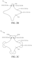
FIG 2B is a schematic view of a second planar structure of first openings of the display panel inFIG 1 ; -
FIG 2C is a schematic view of a third planar structure of first openings of the display panel inFIG 1 ; -
FIG 3A is a cross-sectional view taken along line A-A inFIG 2A ; -
FIG 3B is a cross-sectional view taken along line B-B inFIG 2A ; -
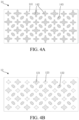
FIG 4A is a schematic diagram of a planar structure of a micro lens layer of a display panel provided by an embodiment of the present application; -
FIG 4B is a schematic diagram of an arrangement of light-emitting pixel units provided by an embodiment of the present application; -
FIG 5 is a schematic diagram of a corresponding structure of a first mask and a display panel provided by an embodiment of the present application; -
FIG 6 is a schematic diagram of a corresponding structure of a second mask and a display panel provided by an embodiment of the present application; -
FIG 7 is a flowchart of a manufacturing method of a display panel provided by an embodiment of the present application; and -
FIG 8A to FIG 8G are schematic flowcharts of a method for manufacturing a display panel provided by an embodiment of the present application. - Description of reference signs:
- 1. display panel; 11, array substrate; 12, light-emitting pixel unit; 121, red light-emitting pixel unit; 122, green light-emitting pixel unit; 123, blue light-emitting pixel unit; 13, encapsulation layer; 14, micro lens layer; 141, micro lens; 142, first opening; 143, second opening; 15, passivation layer; 16, photoresist layer;
- 2. mask plate; 21, first functional area; 22, second functional area; 23, hollow area; 24, shading area; 211, main body portion; 2111, side edge; 2111a, first side; 2111b, second side; 2112, corner; 2112a, first corner; 2112b, second corner; 212, expansion portion; 212a, first sub-expansion portion; 212b, second sub-expansion portion.
- The technical solutions in the embodiments of the present application will be clearly and completely described below in conjunction with the accompanying drawings in the embodiments of the present application. Obviously, the described embodiments are only a part of the embodiments of the present application, rather than all the embodiments. Based on the embodiments in this application, all other embodiments obtained by those skilled in the art without creative work shall fall within the protection scope of this application. In addition, it should be understood that the specific implementations described here are only used to illustrate and explain the application, and are not used to limit the application. In this application, if no explanation is made to the contrary, the orientation words used such as "upper" and "lower" generally refer to the upper and lower positions of the device in actual use or working state, and specifically refer to the drawing directions in the drawings. Further, "inner" and "outer" refer to the outline of the device.
- Please refer to
FIG 1. FIG 1 is a schematic cross-sectional structure diagram of a display panel provided by an embodiment of the present disclosure. An embodiment of the present disclosure provides adisplay panel 1, which includes anarray substrate 11, a plurality of light-emittingpixel units 12, amicro lens layer 14, and apassivation layer 15. - The
array substrate 11 includes a substrate and a plurality of thin film transistors and a plurality of signal wirings provided on the substrate. The thin film transistors are used to drive the corresponding light-emittingpixel units 12 to emit light. A plurality of the light-emittingpixel units 12 are arranged on thearray substrate 11. Themicro lens layer 14 is provided on a side of the light-emittingpixel unit 12 away from thearray substrate 11. Themicro lens layer 14 includes a plurality ofmicro lenses 141 and a plurality of openings. Each of the openings are formed between two adjacent micro lenses 141.The openings are arranged corresponding to the light-emittingpixel units 12. Thepassivation layer 15 covers themicro lens layer 14. - Understandably, the
display panel 1 in the embodiment of the present disclosure passes through the difference in refractive index between themicro lens layer 14 and thepassivation layer 15. In this way, a light emitted by the light-emittingpixel units 12 is totally reflected at the junction of themicro lenses 141 and thepassivation layer 15, so that the light is converged. Specifically, a refractive index of thepassivation layer 15 is greater than the refractive index of themicro lens layer 14. For example, a refractive index of themicro lens layer 14 is 1.5, and the refractive index of thepassivation layer 15 is 1.65. When a planar shape of the opening and a planar shape of the light-emittingpixel units 12 are the same and the size is the same or close to each other, the light emitted by the light-emittingpixel units 12 has the best converging effect at a junction of themicro lenses 141 and thepassivation layer 15. - Since a pattern shape of the light-emitting
pixel unit 12 has corners, correspondingly, the pattern shape of a mask used to form the opening also has corners, and the corners are formed by an intersection of two adjacent side edges. Since an ultraviolet light used in an exposure process will be diffracted at the two adjacent side edges forming the corners, the ultraviolet light bypasses the edges of the two adjacent side edges and spreads to different degrees. Because a relative distance between the two adjacent side edges at the corners is relatively short, the ultraviolet light diffracted from the two adjacent side edges into the mask is superimposed at the corner, resulting in greater intensity of the diffracted light. As a result, the taper angle θ of the etchedmicro lenses 141 is low and extends inward, which affects the light convergence effect of themicro lenses 141. - In view of this, please combine
FIG 1 andFIG 2A~FIG 2C .FIG 2A is a schematic diagram of a first planar structure of a first opening of the display panel inFIG 1 .FIG 2B is a schematic diagram of a second planar structure of a first opening of the display panel inFIG 1 .FIG 2C is a schematic diagram of a third planar structure of a first opening of the display panel inFIG 1 . - The plurality of openings includes a plurality of
first openings 142. In a direction along a plane of thedisplay panel 1, each of thefirst openings 142 includes amain body portion 211 and at least oneexpansion portion 212. A planar shape of themain body portion 211 is the same as a planar shape of a corresponding light-emittingpixel unit 12. Themain body portion 211 includes a plurality of side edges 2111. Acorner 2112 is formed at the intersection of two adjacent side edges 2111. Theexpansion portion 212 is provided at thecorner 2112. Theexpansion portion 212 is an arc-shaped convex surface. - It can be understood that, in the present disclosure, the
expansion portion 212 is provided at thecorner 2112 to perform fine adjustment based on the pattern of themain body portion 211. In one aspect, thefirst openings 142 are close to the light-emittingpixel units 12 in shape, so as to avoid reducing the light condensing effect of themicro lenses 141 due to a large difference between a shape of thefirst openings 142 and the light-emittingpixel units 12. In another aspect, theexpansion portion 212 increases the distance between two adjacent side edges 2111. This can reduce a total amount of light superimposed at thecorner 2112 of the ultraviolet light diffracted into themask 2 by the two adjacent side edges 2111. Therefore, a superimposed intensity of the diffracted light diffused into themask 2 at thecorner 2112 is reduced, and the taper angle θ of themicro lenses 141 is increased. It is beneficial to improve the light condensing effect of themicro lenses 141, thereby improving the luminous efficiency of thedisplay panel 1. - Specifically, the plurality of
side edges 2111 includes a plurality offirst sides 2111a and a plurality ofsecond sides 2111b. Thefirst sides 2111a and two adjacentsecond sides 2111b respectively form afirst corner 2112a and asecond corner 2112b. Theexpansion portion 212 is provided at thefirst corner 2112a and thesecond corner 2112b. - In an embodiment, referring to
FIG 2A , theexpansion portion 212 surrounds thefirst corner 2112a and thesecond corner 2112b. Since a size of thesecond side 2111b is shorter than that of thefirst side 2111a, a distance between thefirst corner 2112a and thesecond corner 2112b is shorter. Therefore, in this embodiment, by providing only oneexpansion portion 212 that simultaneously surrounds thefirst corner 2112a and thesecond corner 2112b. A circle where theexpansion portion 212 is located intersect with a circle where the two adjacentsecond sides 2111b are located, respectively. - It should be noted, the term of "surround" in this embodiment means that a ray formed by taking a vertex of the
first corner 2112a as an end point and extending in any direction away from themain body portion 211 passes through theexpansion portion 212, and a ray formed by using a vertex of thesecond corner 2112b as an end point to extend in any direction away from themain body 211 also pass through theouter expansion portion 212. - In an embodiment, please refer to
FIG 2B . A difference betweenFIG 2B andFIG 2A is that: theexpansion portion 212 is located between the extension lines of the two adjacentfirst sides 2111a, and a circle where theexpansion portion 212 is located is circumscribed to a circle where the two adjacentfirst sides 2111a are located respectively. An area of theexpansion portion 212 inFIG 2A is smaller than an area of theexpansion portion 212 inFIG 2B , which is beneficial to reduce the difference between the formedfirst openings 142 and the corresponding light-emittingpixel units 12, Therefore, the light condensing effect of themicro lenses 141 is further improved. - In an embodiment, please refer to
FIG 2C . A difference betweenFIG 2C andFIG 2A is that: theexpansion portion 212 includes afirst sub-expansion portion 212a and asecond sub-expansion portion 212b connected with each other, wherein thefirst sub-expansion portion 212a surrounds thefirst corner 2112a, and thesecond sub-expansion portion 212b surrounds thesecond corner 2112b. In this embodiment, by arranging two sub-expansion portions surrounding thefirst corner 2112a and thesecond corner 2112b respectively, a circle where thefirst sub-expansion portion 212a is located intersects a circle where one of the two adjacentfirst sides 2111a is located, and a circle where thesecond sub-expansion portion 212b is located intersects a circle where the other one of the two adjacentfirst sides 2111a is located. - It should be noted, the term of "surround" in this embodiment means that a ray formed by taking a vertex of the
first corner 2112a as an end point to extend in any direction away from themain body portion 211 passes through thefirst sub-expansion portion 212a, and a ray formed by taking a vertex of thesecond corner 2112b as an end point and extending in any direction away from themain body portion 211 passes through thesecond sub-expansion portion 212b. In a direction along the plane of themask plate 2, a sum of areas of thefirst sub-expansion portion 212a and thesecond sub-expansion portion 212b inFIG 2C is smaller than that of the expansion portion inFIG 2A . It is beneficial to reduce the difference between the formedfirst openings 142 and the corresponding light-emittingpixel units 12, thereby further improving the light condensing effect of themicro lenses 141. - Specifically, in order to avoid that the
first openings 142 are too different from the corresponding light-emittingpixel units 12, the light condensing effect of themicro lenses 141 is affected. In the embodiment of the present disclosure, a ratio of the area of theexpansion portion 212 to the area of themain body portion 211 is less than or equal to 0.2. - Specifically, in a plane direction perpendicular to the
display panel 1, an angle between a side surface of themicro lenses 141 and a plane where thearray substrate 11 is located ranges from 50 degrees to 90 degrees. - Further, please refer to
FIGS. 3A and 3B. FIG 3A is a cross-sectional view along A-A inFIG 2A .FIG 3B is a cross-sectional view along B-B inFIG 2A . On a cross section perpendicular to the two oppositefirst sides 2111a (along the A-A section line inFIG 2A ), an angle between the side surface of themicro lenses 141 and a plane where thearray substrate 11 is located is the first Angle θ1. On a cross section perpendicular to the two opposite expansion portions 212 (along the B-B section line inFIG 2A ), an angle between the side surface of themicro lenses 141 and a plane where thearray substrate 11 is located is a second angle θ2. - A range of the difference between the first angle θ1 and the second angle θ2 is less than 20 degrees. By adding a design of the
expansion portion 212 to themain body portion 211, the inward extension of themicro lenses 141 can be improved, such that the second angle θ2 decreases and approaches the first angle θ1. It is beneficial to improve the light condensing effect of themicro lenses 141, thereby improving the luminous efficiency of thedisplay panel 1. - Further, the first angle θ1 is equal to the second angle θ2. In the present disclosure, by adding a design of the
expansion portion 212 to themain body portion 211, the inward extension of themicro lenses 141 caused by the diffraction of light can be improved. It is beneficial to further improve the light condensing effect of themicro lenses 141, thereby improving the luminous efficiency of thedisplay panel 1. - Optionally, in the embodiment of the present disclosure, the shape of the
main body 211 is a pearl shape. Of course, in other embodiments, themain body 211 may also have other shapes, which is not limited in the present disclosure. - It should be noted that, in order to clearly illustrate the technical solution of the present disclosure, the embodiment of the present disclosure takes the shape of the
main body portion 211 as a pearl as an example for explanation. - Specifically, the plurality of
side edges 2111 includes fourfirst sides 2111a and foursecond sides 2111b. Thefirst side 2111a and thesecond side 2111b are alternately connected to form a closed figure. Thefirst side 2111a is an arc that is recessed toward the inside of the closed figure. Thesecond side 2111b is a straight line. - Please combine
FIG 1 ,FIG 4A, and FIG 4B. FIG 4A is a schematic diagram of a planar structure of a micro lens layer of a display panel according to an embodiment of the present disclosure.FIG 4B is a schematic diagram of the arrangement of light-emitting pixel units provided by an embodiment of the present disclosure. The plurality of light-emittingpixel units 12 at least includes a plurality of red light-emittingpixel units 121, a plurality of green light-emittingpixel units 122, and a plurality of blue light-emittingpixel units 123. Thefirst openings 142 correspond to the red light-emittingpixel unit 121 and the blue light-emittingpixel unit 123. - The planar shape of the
main body portion 211 is the same as the planar shape of the corresponding light-emittingpixel unit 12. Correspondingly, in the embodiment of the present disclosure, the planar shape of the red light-emittingpixel unit 121 and the blue light-emittingpixel unit 123 is a pearl shape, and the planar shape of the green light-emittingpixel unit 122 may be an ellipse. Of course, the planar shape of the green light-emittingpixel unit 122 may also be other curved shapes. - Specifically, the light-emitting area of the red light-emitting
pixel unit 121 is larger than the light-emitting area of the green light-emittingpixel unit 122. Therefore, in a plane direction of thedisplay panel 1, the area of thefirst opening 142 corresponding to the red light-emittingpixel unit 121 is larger than the area of thefirst opening 142 corresponding to the green light-emittingpixel unit 122. - Further, the
display panel 1 further includes a plurality ofsecond openings 143. Thesecond opening 143 is arranged corresponding to the green light-emittingpixel unit 122. The pattern shape of thesecond opening 143 is the same as the pattern shape of the green light-emittingpixel unit 122. The light-emitting area of the green light-emittingpixel unit 122 is smaller than the light-emitting area of the red light-emittingpixel unit 121 and the blue light-emittingpixel unit 123. Therefore, in the plane direction of thedisplay panel 1, the area of thesecond opening 143 is smaller than the area of thefirst opening 142. - It is understandable that, the shape of the
second opening 143 in the embodiment of the present disclosure is arc-shaped, there is nocorner 2112 of themain body portion 211 in thefirst opening 142. Therefore, thesecond opening 143 does not need to be provided with theexpansion portion 212. - Further, please continue to refer to
FIG 1 . Thedisplay panel 1 further includes anencapsulation layer 13 arranged between the light-emittingpixel unit 12 and themicro lens layer 14. Theencapsulation layer 13 covers the light-emittingpixel units 12 and thearray substrate 11. Themicro lens layer 14 is provided on a side of theencapsulation layer 13 away from thearray substrate 11. - Further, the
display panel 1 may also include portions not shown, such as touch electrodes, a buffer layer, and a color filter layer. - Please refer to
FIG 5 and FIG 6. FIG 5 is a schematic diagram of the corresponding structure of a first mask and a display panel provided by an embodiment of the present disclosure.FIG 6 is a schematic diagram of the corresponding structure of a second mask and a display panel provided by an embodiment of the present disclosure. The embodiment of the present disclosure also provides a mask for forming the opening. The mask includes a firstfunctional area 21 and a secondfunctional area 22. The firstfunctional area 21 corresponds to thefirst opening 142. The second functional area corresponds to thesecond opening 143. A planar shape of the firstfunctional area 21 is the same as the planar shape of thefirst opening 142. A planar shape of the secondfunctional area 22 is the same as the planar shape of the second opening. - In an embodiment, referring to
FIG 5 , the firstfunctional area 21 and the secondfunctional area 22 are light-shielding areas for light-shielding. An area on themask 2 except for the firstfunctional area 21 and the secondfunctional area 22 is ahollow area 23 for light transmission. The photoresist used in a yellow light process for forming themicro lenses 141 is a negative photoresist, so that the ultraviolet light used for the exposure process passes through thehollow area 23 except for the firstfunctional area 21 and the secondfunctional area 22. The photoresist corresponding to thehollow area 23 remains, while the photoresist corresponding to the firstfunctional area 21 and the secondfunctional area 22 is removed. After an etching process, themicro lens layer 14 corresponding to thehollow area 23 is partially retained, and themicro lens layer 14 corresponding to the firstfunctional area 21 and the secondfunctional area 22 is completely removed. At the same time, due to the diffraction effect of light, themicro lens layer 14 near the edges corresponding to the firstfunctional area 21 and the secondfunctional area 22 is partially removed, thereby forming a taper angle θ. - In one embodiment, please refer to
FIG 6 . The firstfunctional area 21 and the secondfunctional area 22 are hollow areas for light transmission. The area on themask 2 except for the firstfunctional area 21 and the secondfunctional area 22 is a light-shieldingarea 24 for light-shielding. The photoresist used in the yellow light process for forming themicro lenses 141 is a positive photoresist, such that the ultraviolet light used for the exposure process passes through the light-shieldingarea 24 except for the firstfunctional area 21 and the secondfunctional area 22. The photoresist corresponding to the light-shieldingarea 24 is removed, while the photoresist corresponding to the firstfunctional area 21 and the secondfunctional area 22 remains. After an etching process, themicro lens layer 14 corresponding to theshading area 24 is completely removed, and themicro lens layer 14 corresponding to the firstfunctional area 21 and the secondfunctional area 22 remains. At the same time, due to the diffraction effect of light, a portion of themicro lens layer 14 near the edge of thelight shielding region 24 remains, thereby forming a taper angle θ. - Please refer to
FIG 7, and FIG 8A toFIG 8G FIG 7 is a flowchart of a method for manufacturing a display panel provided by an embodiment of the present disclosure.FIG 8A to FIG 8G are schematic flowcharts of a manufacturing method of a display panel provided by an embodiment of the present disclosure. The embodiment of the present disclosure also provides a manufacturing method of thedisplay panel 1, including the following steps: - In step S10, an
array substrate 11 is provided. - Specifically, please refer to
FIG 8A . At first, a substrate is provided. A plurality of thin film transistors and a plurality of signal traces are formed on the substrate. The thin film transistor includes a gate, a gate insulating layer, an active layer, a source and drain metal layer, and other film layers, all of which are sequentially formed on the substrate. Since this is a prior art, it will not be described in detail here. - In step S20, a plurality of light-emitting
pixel units 12 are formed on thearray substrate 11. - Specifically, please refer to
FIG 8B . The plurality of light-emittingpixel units 12 includes a red light-emittingpixel unit 121, a green light-emittingpixel unit 122, and a blue light-emittingpixel unit 123. Each of the light-emittingpixel units 12 includes an anode, a pixel definition layer, an electron injection layer, an electron transport layer, an organic light-emitting layer, a hole injection layer, and a hole transport layer. The organic light-emitting layer can be formed by inkjet printing. - Further, after the step S20, the method further includes: forming an
encapsulation layer 13 covering thearray substrate 11 and the light-emittingpixel unit 12. - Specifically, please refer to
FIG 8C . Theencapsulation layer 13 can be encapsulated by a thin film to prevent water vapor from intruding into the organic light-emitting layer of the light-emittingpixel unit 12 to cause the light-emittingpixel unit 12 to fail. Theencapsulation layer 13 can be a single-layer encapsulation or a multi-layer encapsulation, Specifically, when theencapsulation layer 13 adopts multi-layer encapsulation, such as three-layer encapsulation, theencapsulation layer 13 includes a first inorganic encapsulation layer, an organic encapsulation layer, and a second inorganic encapsulation layer that are sequentially formed. - In step S30, a
micro lens layer 14 is formed on a side of the light-emittingpixel unit 12 away from thearray substrate 11, and themicro lens layer 14 includes a plurality ofmicro lenses 141 and a plurality of openings. The openings are formed between two adjacentmicro lenses 141. The openings are arranged corresponding to the light-emittingpixel units 12. - Specifically, refer to
FIG 8D . First, amicro lens layer 14 is formed on an entire surface of theencapsulation layer 13, and aphotoresist layer 16 is formed on an entire surface of themicro lens layer 14. Please refer toFIG 8E , and then themask 2 is used to expose thephotoresist layer 16 so that thephotoresist layer 16 corresponding to the light-emittingpixel unit 12 is exposed. Referring toFIG 8F , thephotoresist layer 16 is stripped, and finally themicro lens layer 14 is etched with an etching solution, so that themicro lens layer 14 corresponding to the light-emittingpixel unit 12 is etched away. Thus, a plurality of themicro lenses 141 are formed, and the openings are formed between two adjacentmicro lenses 141, and the plurality of openings include a plurality offirst openings 142 and a plurality ofsecond openings 143. - In step S40, a
passivation layer 15 covering theencapsulation layer 13 and themicro lens layer 14 is formed. - Specifically, please refer to
FIG 8G Thepassivation layer 15 can be formed by a process of deposition, sputtering, or evaporation. Thepassivation layer 15 is an inorganic material. A refractive index of thepassivation layer 15 is greater than a refractive index of themicro lens layer 14, so that the light emitted by the light-emittingpixel unit 12 converges at the boundary between themicro lenses 141 and thepassivation layer 15. It is beneficial to improve the light extraction efficiency of thedisplay panel 1. - In an embodiment, before forming the
micro lens layer 14 on theencapsulation layer 13, the preparation method further includes the following steps: forming a touch layer on the encapsulation layer 13 (not shown in the figure). Specifically, the touch layer may adopt a DOT (Direct On Cell Touch, directly fabricating the touch layer on the encapsulation layer 13) structure, and thedisplay panel 1 is a touch display panel. - It can be understood that the shape of the opening is the same as the shape of the corresponding light-emitting
pixel unit 12 in thedisplay panel 1 formed by using the above-mentionedmask plate 2. It is beneficial to improve the light condensing effect of themicro lenses 141, thereby improving the luminous efficiency of thedisplay panel 1. - The present disclosure also provides a display device. The display device includes the display panel in the above embodiment. The display device can be any product or component with a display function, such as a mobile phone, a tablet computer, a television, a monitor, a notebook computer, a digital photo frame, a navigator, and the like.
- The display device further includes a touch panel, which is combined with the display panel in a built-in or externally mounted manner, so that the display device has a touch function.
- Beneficial effects are that: in the display panel and the display device provided in the present disclosure, the display panel includes a micro lens layer and a passivation layer, the micro lens layer includes a plurality of micro lenses and a plurality of openings, and the plurality of openings includes a plurality of first openings, where each of the first openings includes a main body. In the present disclosure, by setting an expansion portion at the corner to fine-tune a shape of the first opening based on a pattern of the main body portion. In one aspect, the first openings are made to be close to the light-emitting pixel unit in shape, so as to avoid reducing a light condensing effect of the micro lenses due to a large difference between the shape of the first openings and the light-emitting pixel units. In another aspect, forming a flared portion at the corner of the main body portion increases a distance between adjacent side edges, which can reduce a superimposed intensity of a diffracted light diffused into a mask at the corner, thereby improving the taper angle of the micro lenses. It is beneficial to improve a light condensing effect of the micro lenses, thereby improving a luminous efficiency of the display panel.
- From above, although the present disclosure has been disclosed as above in preferred embodiments, the above-mentioned preferred embodiments are not intended to limit the present disclosure. Those of ordinary skill in the art can make various changes and modifications without departing from the spirit and scope of the present disclosure. Therefore, the protection scope of the present disclosure is subject to the scope defined by the claims.
Claims (20)
- A display panel, comprising:an array substrate;a plurality of light-emitting pixel units arranged on the array substrate;a micro lens layer arranged on a side of the light-emitting pixel units away from the array substrate, wherein the micro lens layer comprises a plurality of micro lenses and a plurality of openings, the openings are formed between two adjacent micro lenses, and the openings are arranged corresponding to the light-emitting pixel units;a passivation layer covering the micro lens layer, wherein a refractive index of the passivation layer is greater than a refractive index of the micro lens layer; and an encapsulation layer covering the light-emitting pixel units and the array substrate,wherein the plurality of openings include a plurality of first openings, and in a direction along a plane of the display panel, each of the first openings includes a main body portion and at least one expansion portion, wherein the main body portion includes a plurality of side edges, and a corner is formed at the intersection of two adjacent side edges, wherein the expansion portion is arranged at the corner, and the expansion portion is an arc-shaped convex surface.
- The display panel according to Claim 1, wherein the plurality of side edges include a plurality of first sides and a plurality of second sides, and the first sides and two adjacent second sides respectively form a first corner and a second corner, wherein the expansion portion is provided at the first corner and the second corner.
- The display panel according to Claim 2, wherein the expansion portion surrounds the first corner and the second corner.
- The display panel according to Claim 2, wherein the expansion portion is located between two adjacent extension lines of the first side, and a circle where the expansion portion is located is circumscribed to a circle where the two adjacent first sides are located, respectively.
- The display panel according to Claim 2, wherein the expansion portion at least comprises a first sub-expansion portion and a second sub-expansion portion connected with each other, wherein the first sub-expansion portion surrounds the first corner, and the second sub-expansion portion surrounds the second corner.
- The display panel according to Claim 1, wherein a ratio of an area of the expansion portion to an area of the main body portion is less than or equal to 0.2.
- The display panel according to Claim 2, wherein an angle between a side surface of the micro lenses and a plane where the array substrate is located is in a range of 50 degrees to 90 degrees.
- A display panel, comprising:an array substrate;a plurality of light-emitting pixel units arranged on the array substrate;a micro lens layer arranged on a side of the light-emitting pixel units away from the array substrate, wherein the micro lens layer comprises a plurality of micro lenses and a plurality of openings, the openings are formed between two adjacent micro lenses, and the openings are arranged corresponding to the light-emitting pixel units; anda passivation layer covering the micro lens layer, wherein a refractive index of the passivation layer is greater than a refractive index of the micro lens layer,wherein the plurality of openings include a plurality of first openings, and in a direction along a plane of the display panel, each of the first openings includes a main body portion and at least one expansion portion, wherein the main body portion includes a plurality of side edges, and a corner is formed at the intersection of two adjacent side edges, wherein the expansion portion is arranged at the corner, and the expansion portion is an arc-shaped convex surface.
- The display panel according to Claim 8, wherein the plurality of side edges include a plurality of first sides and a plurality of second sides, and the first sides and two adjacent second sides respectively form a first corner and a second corner, wherein the expansion portion is provided at the first corner and the second corner.
- The display panel according to Claim 9, wherein the expansion portion surrounds the first corner and the second corner.
- The display panel according to Claim 9, wherein the expansion portion is located between two adjacent extension lines of the first side, and a circle where the expansion portion is located is circumscribed to a circle where the two adjacent first sides are located, respectively.
- The display panel according to Claim 9, wherein the expansion portion at least comprises a first sub-expansion portion and a second sub-expansion portion connected with each other, wherein the first sub-expansion portion surrounds the first corner, and the second sub-expansion portion surrounds the second corner.
- The display panel according to Claim 8, wherein a ratio of an area of the expansion portion to an area of the main body portion is less than or equal to 0.2.
- The display panel according to Claim 9, wherein an angle between a side surface of the micro lenses and a plane where the array substrate is located is in a range of 50 degrees to 90 degrees.
- The display panel according to Claim 14, wherein on a cross-section perpendicular to the two opposite first sides, an angle between the side surface of the micro lenses and the plane where the array substrate is located is a first angle; wherein on a cross-section perpendicular to the two opposite expansion portions, an angle between the side surface of the micro lenses and the plane where the array substrate is located is a second angle; and wherein, a range of a difference between the first angle and the second angle is less than 20 degrees.
- The display panel according to Claim 15, wherein the first angle and the second angle are equal.
- The display panel according to Claim 9, wherein the plurality of side edges include four first sides and four second sides, wherein the four first sides and the four second sides are alternately connected to form a closed figure, and the first sides are arc lines recessed toward an inside of the closed figure.
- The display panel according to Claim 17, wherein a planar shape of the main body portion is the same as a planar shape of corresponding light-emitting pixel units.
- The display panel according to Claim 8, wherein the openings further comprise a second opening, and a planar shape of the second opening is an ellipse or a circle; and the plurality of light-emitting pixel units at least include a red light-emitting pixel unit, a green light-emitting pixel unit, and a blue light-emitting pixel unit, wherein the first openings correspond to the red light-emitting pixel unit and the green light-emitting pixel unit, and the second opening corresponds to the blue light-emitting pixel unit.
- A display device, comprising a display panel, wherein the display panel comprises:an array substrate;a plurality of light-emitting pixel units arranged on the array substrate;a micro lens layer arranged on a side of the light-emitting pixel units away from the array substrate, wherein the micro lens layer comprises a plurality of micro lenses and a plurality of openings, the openings are formed between two adjacent micro lenses, and the openings are arranged corresponding to the light-emitting pixel units; anda passivation layer covering the micro lens layer, wherein a refractive index of the passivation layer is greater than a refractive index of the micro lens layer,wherein the plurality of openings include a plurality of first openings, and in a direction along a plane of the display panel, each of the first openings includes a main body portion and at least one expansion portion, wherein the main body portion includes a plurality of side edges, and a corner is formed at the intersection of two adjacent side edges, wherein the expansion portion is arranged at the corner, and the expansion portion is an arc-shaped convex surface.
Applications Claiming Priority (2)
| Application Number | Priority Date | Filing Date | Title |
|---|---|---|---|
| CN202111029964.5A CN113745431B (en) | 2021-09-03 | 2021-09-03 | Display panel and display device |
| PCT/CN2021/118394 WO2023029092A1 (en) | 2021-09-03 | 2021-09-15 | Display panel and display device |
Publications (2)
| Publication Number | Publication Date |
|---|---|
| EP4398284A1 true EP4398284A1 (en) | 2024-07-10 |
| EP4398284A4 EP4398284A4 (en) | 2025-07-23 |
Family
ID=78735209
Family Applications (1)
| Application Number | Title | Priority Date | Filing Date |
|---|---|---|---|
| EP21839808.9A Pending EP4398284A4 (en) | 2021-09-03 | 2021-09-15 | SCOREBOARD AND DISPLAY DEVICE |
Country Status (6)
| Country | Link |
|---|---|
| US (1) | US12035606B2 (en) |
| EP (1) | EP4398284A4 (en) |
| JP (1) | JP7385732B2 (en) |
| KR (1) | KR102663377B1 (en) |
| CN (1) | CN113745431B (en) |
| WO (1) | WO2023029092A1 (en) |
Families Citing this family (2)
| Publication number | Priority date | Publication date | Assignee | Title |
|---|---|---|---|---|
| CN115000136B (en) * | 2022-05-26 | 2025-07-29 | 武汉天马微电子有限公司 | Display panel, manufacturing method thereof and electronic equipment |
| KR102922107B1 (en) * | 2023-01-18 | 2026-02-04 | 삼성디스플레이 주식회사 | Light emitting display device |
Family Cites Families (16)
| Publication number | Priority date | Publication date | Assignee | Title |
|---|---|---|---|---|
| JP2761453B2 (en) | 1993-11-17 | 1998-06-04 | 出光興産株式会社 | Organic EL element and organic EL panel |
| JP2009294624A (en) * | 2008-06-09 | 2009-12-17 | Sharp Corp | Microlens forming method, solid imaging element and manufacturing method therefor, display device and manufacturing method therefor, and electronic information apparatus |
| TWI607233B (en) * | 2015-02-16 | 2017-12-01 | 財團法人工業技術研究院 | Optical film structure and display structure |
| CN106405853A (en) * | 2016-11-29 | 2017-02-15 | 武汉华星光电技术有限公司 | Stereoscopic display device |
| KR102433274B1 (en) * | 2017-11-28 | 2022-08-18 | 삼성디스플레이 주식회사 | Organic light emitting display device |
| KR102588082B1 (en) * | 2018-09-06 | 2023-10-11 | 엘지디스플레이 주식회사 | Organic light emitting display device and method for manufacturing thereof |
| KR102637859B1 (en) * | 2018-12-17 | 2024-02-19 | 삼성디스플레이 주식회사 | Organic light emitting display device |
| KR102787860B1 (en) * | 2019-01-16 | 2025-04-01 | 삼성디스플레이 주식회사 | Organic light emitting display apparatus |
| KR102758041B1 (en) * | 2019-04-30 | 2025-01-23 | 삼성디스플레이 주식회사 | Display device |
| CN209607764U (en) * | 2019-05-10 | 2019-11-08 | 江苏集萃有机光电技术研究所有限公司 | A kind of OLED luminescent device |
| CN110854298A (en) | 2019-11-26 | 2020-02-28 | 京东方科技集团股份有限公司 | A display panel and display device |
| KR102797539B1 (en) * | 2020-02-12 | 2025-04-21 | 삼성디스플레이 주식회사 | display device and electric apparatus |
| CN115188913B (en) * | 2020-05-06 | 2025-10-03 | 湖北长江新型显示产业创新中心有限公司 | Display panel and display device |
| CN111769143B (en) * | 2020-06-23 | 2022-09-09 | 武汉华星光电半导体显示技术有限公司 | Display panel and manufacturing method thereof |
| CN111834544B (en) * | 2020-06-30 | 2022-08-23 | 湖北长江新型显示产业创新中心有限公司 | Display panel and display device |
| CN113241354B (en) * | 2021-04-07 | 2022-07-12 | 武汉华星光电技术有限公司 | OLED display panel and preparation method thereof |
-
2021
- 2021-09-03 CN CN202111029964.5A patent/CN113745431B/en active Active
- 2021-09-15 WO PCT/CN2021/118394 patent/WO2023029092A1/en not_active Ceased
- 2021-09-15 JP JP2022502948A patent/JP7385732B2/en active Active
- 2021-09-15 EP EP21839808.9A patent/EP4398284A4/en active Pending
- 2021-09-15 US US17/599,588 patent/US12035606B2/en active Active
- 2021-09-15 KR KR1020227002659A patent/KR102663377B1/en active Active
Also Published As
| Publication number | Publication date |
|---|---|
| JP7385732B2 (en) | 2023-11-22 |
| US12035606B2 (en) | 2024-07-09 |
| JP2023542565A (en) | 2023-10-11 |
| CN113745431A (en) | 2021-12-03 |
| EP4398284A4 (en) | 2025-07-23 |
| WO2023029092A1 (en) | 2023-03-09 |
| KR102663377B1 (en) | 2024-05-10 |
| KR20230035208A (en) | 2023-03-13 |
| CN113745431B (en) | 2022-08-23 |
| US20240032399A1 (en) | 2024-01-25 |
Similar Documents
| Publication | Publication Date | Title |
|---|---|---|
| CN114899340B (en) | Display panel and display device | |
| US20260006995A1 (en) | Display panel and manufacturing method therefor, and display device | |
| US11302822B2 (en) | Thin film transistor and fabrication method thereof, array substrate and fabrication method thereof | |
| CN115568245B (en) | Display panel and display device | |
| WO2022247180A1 (en) | Display panel and display device | |
| WO2021120241A1 (en) | Display panel and preparation method therefor | |
| WO2023173459A1 (en) | Display panel and display apparatus | |
| US20240172529A1 (en) | Display panel and display device | |
| US9099404B2 (en) | Array substrate and manufacturing method thereof, OLED display device | |
| WO2022001466A1 (en) | Display device, display panel, and manufacturing method therefor | |
| WO2023184594A1 (en) | Display panel and display apparatus | |
| CN111785760A (en) | A display substrate, its preparation method, and display device | |
| US12035606B2 (en) | Display panel and display device | |
| US20230345776A1 (en) | Display panel, display device and method for manufacturing display pane | |
| US20250301894A1 (en) | Display panel, manufacturing method thereof and display device | |
| WO2020177666A1 (en) | Pixel unit and manufacturing method therefor, and display substrate | |
| WO2025139859A1 (en) | Display panel, manufacturing method therefor and display apparatus | |
| US20240036423A1 (en) | Array substrate and manufacturing method thereof | |
| CN107688263B (en) | display panel | |
| US20250380578A1 (en) | Array base plane, method for preparing array base plane, display panel, and terminal device | |
| WO2025218432A1 (en) | Display panel and display apparatus | |
| WO2024103788A1 (en) | Display panel and display device | |
| US20250204047A1 (en) | Display panel, array substrate and method for manufacturing array substrate | |
| EA049257B1 (en) | DISPLAY PANEL AND DISPLAY DEVICE | |
| CN223829751U (en) | Display substrate and display device |
Legal Events
| Date | Code | Title | Description |
|---|---|---|---|
| STAA | Information on the status of an ep patent application or granted ep patent |
Free format text: STATUS: UNKNOWN |
|
| STAA | Information on the status of an ep patent application or granted ep patent |
Free format text: STATUS: THE INTERNATIONAL PUBLICATION HAS BEEN MADE |
|
| PUAI | Public reference made under article 153(3) epc to a published international application that has entered the european phase |
Free format text: ORIGINAL CODE: 0009012 |
|
| STAA | Information on the status of an ep patent application or granted ep patent |
Free format text: STATUS: REQUEST FOR EXAMINATION WAS MADE |
|
| 17P | Request for examination filed |
Effective date: 20220119 |
|
| AK | Designated contracting states |
Kind code of ref document: A1 Designated state(s): AL AT BE BG CH CY CZ DE DK EE ES FI FR GB GR HR HU IE IS IT LI LT LU LV MC MK MT NL NO PL PT RO RS SE SI SK SM TR |
|
| DAV | Request for validation of the european patent (deleted) | ||
| DAX | Request for extension of the european patent (deleted) | ||
| REG | Reference to a national code |
Ref country code: DE Ref legal event code: R079 Free format text: PREVIOUS MAIN CLASS: H99Z9999999999 Ipc: H10K0050858000 |
|
| A4 | Supplementary search report drawn up and despatched |
Effective date: 20250624 |
|
| RIC1 | Information provided on ipc code assigned before grant |
Ipc: H10K 50/858 20230101AFI20250617BHEP |
|
| GRAP | Despatch of communication of intention to grant a patent |
Free format text: ORIGINAL CODE: EPIDOSNIGR1 |
|
| STAA | Information on the status of an ep patent application or granted ep patent |
Free format text: STATUS: GRANT OF PATENT IS INTENDED |