EP4398030A1 - Optical phase shifter with one or more integrated thermoelectric devices - Google Patents
Optical phase shifter with one or more integrated thermoelectric devices Download PDFInfo
- Publication number
- EP4398030A1 EP4398030A1 EP23205376.9A EP23205376A EP4398030A1 EP 4398030 A1 EP4398030 A1 EP 4398030A1 EP 23205376 A EP23205376 A EP 23205376A EP 4398030 A1 EP4398030 A1 EP 4398030A1
- Authority
- EP
- European Patent Office
- Prior art keywords
- pillars
- waveguide core
- branch
- dielectric layer
- doped region
- Prior art date
- Legal status (The legal status is an assumption and is not a legal conclusion. Google has not performed a legal analysis and makes no representation as to the accuracy of the status listed.)
- Pending
Links
Images








Classifications
-
- G—PHYSICS
- G02—OPTICS
- G02F—OPTICAL DEVICES OR ARRANGEMENTS FOR THE CONTROL OF LIGHT BY MODIFICATION OF THE OPTICAL PROPERTIES OF THE MEDIA OF THE ELEMENTS INVOLVED THEREIN; NON-LINEAR OPTICS; FREQUENCY-CHANGING OF LIGHT; OPTICAL LOGIC ELEMENTS; OPTICAL ANALOGUE/DIGITAL CONVERTERS
- G02F1/00—Devices or arrangements for the control of the intensity, colour, phase, polarisation or direction of light arriving from an independent light source, e.g. switching, gating or modulating; Non-linear optics
- G02F1/01—Devices or arrangements for the control of the intensity, colour, phase, polarisation or direction of light arriving from an independent light source, e.g. switching, gating or modulating; Non-linear optics for the control of the intensity, phase, polarisation or colour
- G02F1/21—Devices or arrangements for the control of the intensity, colour, phase, polarisation or direction of light arriving from an independent light source, e.g. switching, gating or modulating; Non-linear optics for the control of the intensity, phase, polarisation or colour by interference
- G02F1/212—Mach-Zehnder type
-
- F—MECHANICAL ENGINEERING; LIGHTING; HEATING; WEAPONS; BLASTING
- F25—REFRIGERATION OR COOLING; COMBINED HEATING AND REFRIGERATION SYSTEMS; HEAT PUMP SYSTEMS; MANUFACTURE OR STORAGE OF ICE; LIQUEFACTION SOLIDIFICATION OF GASES
- F25B—REFRIGERATION MACHINES, PLANTS OR SYSTEMS; COMBINED HEATING AND REFRIGERATION SYSTEMS; HEAT PUMP SYSTEMS
- F25B21/00—Machines, plants or systems, using electric or magnetic effects
- F25B21/02—Machines, plants or systems, using electric or magnetic effects using Peltier effect; using Nernst-Ettinghausen effect
- F25B21/04—Machines, plants or systems, using electric or magnetic effects using Peltier effect; using Nernst-Ettinghausen effect reversible
-
- G—PHYSICS
- G02—OPTICS
- G02F—OPTICAL DEVICES OR ARRANGEMENTS FOR THE CONTROL OF LIGHT BY MODIFICATION OF THE OPTICAL PROPERTIES OF THE MEDIA OF THE ELEMENTS INVOLVED THEREIN; NON-LINEAR OPTICS; FREQUENCY-CHANGING OF LIGHT; OPTICAL LOGIC ELEMENTS; OPTICAL ANALOGUE/DIGITAL CONVERTERS
- G02F1/00—Devices or arrangements for the control of the intensity, colour, phase, polarisation or direction of light arriving from an independent light source, e.g. switching, gating or modulating; Non-linear optics
- G02F1/01—Devices or arrangements for the control of the intensity, colour, phase, polarisation or direction of light arriving from an independent light source, e.g. switching, gating or modulating; Non-linear optics for the control of the intensity, phase, polarisation or colour
- G02F1/0121—Operation of devices; Circuit arrangements, not otherwise provided for in this subclass
-
- G—PHYSICS
- G02—OPTICS
- G02F—OPTICAL DEVICES OR ARRANGEMENTS FOR THE CONTROL OF LIGHT BY MODIFICATION OF THE OPTICAL PROPERTIES OF THE MEDIA OF THE ELEMENTS INVOLVED THEREIN; NON-LINEAR OPTICS; FREQUENCY-CHANGING OF LIGHT; OPTICAL LOGIC ELEMENTS; OPTICAL ANALOGUE/DIGITAL CONVERTERS
- G02F1/00—Devices or arrangements for the control of the intensity, colour, phase, polarisation or direction of light arriving from an independent light source, e.g. switching, gating or modulating; Non-linear optics
- G02F1/01—Devices or arrangements for the control of the intensity, colour, phase, polarisation or direction of light arriving from an independent light source, e.g. switching, gating or modulating; Non-linear optics for the control of the intensity, phase, polarisation or colour
- G02F1/0147—Devices or arrangements for the control of the intensity, colour, phase, polarisation or direction of light arriving from an independent light source, e.g. switching, gating or modulating; Non-linear optics for the control of the intensity, phase, polarisation or colour based on thermo-optic effects
-
- G—PHYSICS
- G02—OPTICS
- G02F—OPTICAL DEVICES OR ARRANGEMENTS FOR THE CONTROL OF LIGHT BY MODIFICATION OF THE OPTICAL PROPERTIES OF THE MEDIA OF THE ELEMENTS INVOLVED THEREIN; NON-LINEAR OPTICS; FREQUENCY-CHANGING OF LIGHT; OPTICAL LOGIC ELEMENTS; OPTICAL ANALOGUE/DIGITAL CONVERTERS
- G02F1/00—Devices or arrangements for the control of the intensity, colour, phase, polarisation or direction of light arriving from an independent light source, e.g. switching, gating or modulating; Non-linear optics
- G02F1/01—Devices or arrangements for the control of the intensity, colour, phase, polarisation or direction of light arriving from an independent light source, e.g. switching, gating or modulating; Non-linear optics for the control of the intensity, phase, polarisation or colour
- G02F1/015—Devices or arrangements for the control of the intensity, colour, phase, polarisation or direction of light arriving from an independent light source, e.g. switching, gating or modulating; Non-linear optics for the control of the intensity, phase, polarisation or colour based on semiconductor elements having potential barriers, e.g. having a PN or PIN junction
- G02F1/025—Devices or arrangements for the control of the intensity, colour, phase, polarisation or direction of light arriving from an independent light source, e.g. switching, gating or modulating; Non-linear optics for the control of the intensity, phase, polarisation or colour based on semiconductor elements having potential barriers, e.g. having a PN or PIN junction in an optical waveguide structure
-
- G—PHYSICS
- G02—OPTICS
- G02F—OPTICAL DEVICES OR ARRANGEMENTS FOR THE CONTROL OF LIGHT BY MODIFICATION OF THE OPTICAL PROPERTIES OF THE MEDIA OF THE ELEMENTS INVOLVED THEREIN; NON-LINEAR OPTICS; FREQUENCY-CHANGING OF LIGHT; OPTICAL LOGIC ELEMENTS; OPTICAL ANALOGUE/DIGITAL CONVERTERS
- G02F1/00—Devices or arrangements for the control of the intensity, colour, phase, polarisation or direction of light arriving from an independent light source, e.g. switching, gating or modulating; Non-linear optics
- G02F1/01—Devices or arrangements for the control of the intensity, colour, phase, polarisation or direction of light arriving from an independent light source, e.g. switching, gating or modulating; Non-linear optics for the control of the intensity, phase, polarisation or colour
- G02F1/21—Devices or arrangements for the control of the intensity, colour, phase, polarisation or direction of light arriving from an independent light source, e.g. switching, gating or modulating; Non-linear optics for the control of the intensity, phase, polarisation or colour by interference
- G02F1/225—Devices or arrangements for the control of the intensity, colour, phase, polarisation or direction of light arriving from an independent light source, e.g. switching, gating or modulating; Non-linear optics for the control of the intensity, phase, polarisation or colour by interference in an optical waveguide structure
-
- G—PHYSICS
- G02—OPTICS
- G02F—OPTICAL DEVICES OR ARRANGEMENTS FOR THE CONTROL OF LIGHT BY MODIFICATION OF THE OPTICAL PROPERTIES OF THE MEDIA OF THE ELEMENTS INVOLVED THEREIN; NON-LINEAR OPTICS; FREQUENCY-CHANGING OF LIGHT; OPTICAL LOGIC ELEMENTS; OPTICAL ANALOGUE/DIGITAL CONVERTERS
- G02F1/00—Devices or arrangements for the control of the intensity, colour, phase, polarisation or direction of light arriving from an independent light source, e.g. switching, gating or modulating; Non-linear optics
- G02F1/01—Devices or arrangements for the control of the intensity, colour, phase, polarisation or direction of light arriving from an independent light source, e.g. switching, gating or modulating; Non-linear optics for the control of the intensity, phase, polarisation or colour
- G02F1/21—Devices or arrangements for the control of the intensity, colour, phase, polarisation or direction of light arriving from an independent light source, e.g. switching, gating or modulating; Non-linear optics for the control of the intensity, phase, polarisation or colour by interference
- G02F1/225—Devices or arrangements for the control of the intensity, colour, phase, polarisation or direction of light arriving from an independent light source, e.g. switching, gating or modulating; Non-linear optics for the control of the intensity, phase, polarisation or colour by interference in an optical waveguide structure
- G02F1/2257—Devices or arrangements for the control of the intensity, colour, phase, polarisation or direction of light arriving from an independent light source, e.g. switching, gating or modulating; Non-linear optics for the control of the intensity, phase, polarisation or colour by interference in an optical waveguide structure the optical waveguides being made of semiconducting material
-
- H—ELECTRICITY
- H10—SEMICONDUCTOR DEVICES; ELECTRIC SOLID-STATE DEVICES NOT OTHERWISE PROVIDED FOR
- H10N—ELECTRIC SOLID-STATE DEVICES NOT OTHERWISE PROVIDED FOR
- H10N10/00—Thermoelectric devices comprising a junction of dissimilar materials, i.e. devices exhibiting Seebeck or Peltier effects
- H10N10/10—Thermoelectric devices comprising a junction of dissimilar materials, i.e. devices exhibiting Seebeck or Peltier effects operating with only the Peltier or Seebeck effects
- H10N10/17—Thermoelectric devices comprising a junction of dissimilar materials, i.e. devices exhibiting Seebeck or Peltier effects operating with only the Peltier or Seebeck effects characterised by the structure or configuration of the cell or thermocouple forming the device
-
- H—ELECTRICITY
- H10—SEMICONDUCTOR DEVICES; ELECTRIC SOLID-STATE DEVICES NOT OTHERWISE PROVIDED FOR
- H10N—ELECTRIC SOLID-STATE DEVICES NOT OTHERWISE PROVIDED FOR
- H10N10/00—Thermoelectric devices comprising a junction of dissimilar materials, i.e. devices exhibiting Seebeck or Peltier effects
- H10N10/80—Constructional details
- H10N10/85—Thermoelectric active materials
- H10N10/851—Thermoelectric active materials comprising inorganic compositions
- H10N10/852—Thermoelectric active materials comprising inorganic compositions comprising tellurium, selenium or sulfur
-
- H—ELECTRICITY
- H10—SEMICONDUCTOR DEVICES; ELECTRIC SOLID-STATE DEVICES NOT OTHERWISE PROVIDED FOR
- H10N—ELECTRIC SOLID-STATE DEVICES NOT OTHERWISE PROVIDED FOR
- H10N10/00—Thermoelectric devices comprising a junction of dissimilar materials, i.e. devices exhibiting Seebeck or Peltier effects
- H10N10/80—Constructional details
- H10N10/85—Thermoelectric active materials
- H10N10/851—Thermoelectric active materials comprising inorganic compositions
- H10N10/8556—Thermoelectric active materials comprising inorganic compositions comprising compounds containing germanium or silicon
-
- G—PHYSICS
- G02—OPTICS
- G02B—OPTICAL ELEMENTS, SYSTEMS OR APPARATUS
- G02B6/00—Light guides; Structural details of arrangements comprising light guides and other optical elements, e.g. couplings
- G02B6/10—Light guides; Structural details of arrangements comprising light guides and other optical elements, e.g. couplings of the optical waveguide type
- G02B6/12—Light guides; Structural details of arrangements comprising light guides and other optical elements, e.g. couplings of the optical waveguide type of the integrated circuit kind
- G02B6/122—Basic optical elements, e.g. light-guiding paths
- G02B6/125—Bends, branchings or intersections
-
- G—PHYSICS
- G02—OPTICS
- G02F—OPTICAL DEVICES OR ARRANGEMENTS FOR THE CONTROL OF LIGHT BY MODIFICATION OF THE OPTICAL PROPERTIES OF THE MEDIA OF THE ELEMENTS INVOLVED THEREIN; NON-LINEAR OPTICS; FREQUENCY-CHANGING OF LIGHT; OPTICAL LOGIC ELEMENTS; OPTICAL ANALOGUE/DIGITAL CONVERTERS
- G02F1/00—Devices or arrangements for the control of the intensity, colour, phase, polarisation or direction of light arriving from an independent light source, e.g. switching, gating or modulating; Non-linear optics
- G02F1/01—Devices or arrangements for the control of the intensity, colour, phase, polarisation or direction of light arriving from an independent light source, e.g. switching, gating or modulating; Non-linear optics for the control of the intensity, phase, polarisation or colour
- G02F1/015—Devices or arrangements for the control of the intensity, colour, phase, polarisation or direction of light arriving from an independent light source, e.g. switching, gating or modulating; Non-linear optics for the control of the intensity, phase, polarisation or colour based on semiconductor elements having potential barriers, e.g. having a PN or PIN junction
- G02F1/0151—Devices or arrangements for the control of the intensity, colour, phase, polarisation or direction of light arriving from an independent light source, e.g. switching, gating or modulating; Non-linear optics for the control of the intensity, phase, polarisation or colour based on semiconductor elements having potential barriers, e.g. having a PN or PIN junction modulating the refractive index
-
- G—PHYSICS
- G02—OPTICS
- G02F—OPTICAL DEVICES OR ARRANGEMENTS FOR THE CONTROL OF LIGHT BY MODIFICATION OF THE OPTICAL PROPERTIES OF THE MEDIA OF THE ELEMENTS INVOLVED THEREIN; NON-LINEAR OPTICS; FREQUENCY-CHANGING OF LIGHT; OPTICAL LOGIC ELEMENTS; OPTICAL ANALOGUE/DIGITAL CONVERTERS
- G02F2202/00—Materials and properties
- G02F2202/10—Materials and properties semiconductor
-
- G—PHYSICS
- G02—OPTICS
- G02F—OPTICAL DEVICES OR ARRANGEMENTS FOR THE CONTROL OF LIGHT BY MODIFICATION OF THE OPTICAL PROPERTIES OF THE MEDIA OF THE ELEMENTS INVOLVED THEREIN; NON-LINEAR OPTICS; FREQUENCY-CHANGING OF LIGHT; OPTICAL LOGIC ELEMENTS; OPTICAL ANALOGUE/DIGITAL CONVERTERS
- G02F2203/00—Function characteristic
- G02F2203/21—Thermal instability, i.e. DC drift, of an optical modulator; Arrangements or methods for the reduction thereof
-
- G—PHYSICS
- G02—OPTICS
- G02F—OPTICAL DEVICES OR ARRANGEMENTS FOR THE CONTROL OF LIGHT BY MODIFICATION OF THE OPTICAL PROPERTIES OF THE MEDIA OF THE ELEMENTS INVOLVED THEREIN; NON-LINEAR OPTICS; FREQUENCY-CHANGING OF LIGHT; OPTICAL LOGIC ELEMENTS; OPTICAL ANALOGUE/DIGITAL CONVERTERS
- G02F2203/00—Function characteristic
- G02F2203/50—Phase-only modulation
Definitions
- the disclosure relates to photonics chips and, more specifically, to structures including an optical phase shifter and methods of forming a structure including an optical phase shifter.
- the structure may further comprise a first power supply coupled to the first series circuit, the first power supply configured to supply a current to the first plurality of pillars and the second plurality of pillars of the first thermoelectric device to generate heat for elevating the temperature of the first branch of the waveguide core. Additionally, the structure may further comprise a second power supply coupled to the second series circuit, the second power supply configured to supply a current to the first plurality of pillars and the second plurality of pillars of the second thermoelectric device to extract heat for cooling the second branch of the waveguide core.
- the structure may further comprise a power supply coupled to the first series circuit; the power supply may be configured to: supply a current to the first plurality of pillars and the second plurality of pillars to generate heat for elevating the temperature of the first branch of the waveguide core, or to supply a current to the first plurality of pillars and the second plurality of pillars to extract heat for cooling the first branch of the waveguide core.
- the structure may further comprise a semiconductor substrate, and a dielectric layer on the semiconductor substrate, wherein the dielectric layer may be positioned between the plurality of silicide layers and the semiconductor substrate, and/or wherein the plurality of silicide layers may be positioned between the dielectric layer and the plurality of adjacent pairs of the first plurality of pillars and the second plurality of pillars.
- the structure may further comprise a dielectric layer on the waveguide core, the first plurality of pillars, and the second plurality of pillars, wherein the waveguide core, the first plurality of pillars, and the second plurality of pillars may be embedded in the dielectric layer.
- the structure may further comprise a semiconductor substrate, and a dielectric layer on the semiconductor substrate, wherein the dielectric layer is positioned between the first plurality of pillars and the semiconductor substrate, and the dielectric layer is positioned between the second plurality of pillars and the semiconductor substrate.
- the first plurality of pillars and the second plurality of pillars may be disposed directly on the dielectric layer.
- a structure 10 includes a waveguide core 12 that is positioned on, and above, a dielectric layer 16 and a semiconductor substrate 18.
- the dielectric layer 16 may be comprised of a dielectric material, such as silicon dioxide, and the semiconductor substrate 18 may be comprised of a semiconductor material, such as single-crystal silicon.
- the dielectric layer 16 may be a buried oxide layer of a silicon-on-insulator substrate, and the dielectric layer 16 may separate the waveguide core 12 from the semiconductor substrate 18.
- a portion of the waveguide core 12 may configured to function as an optical phase shifter, such as a Mach-Zehnder modulator.
- a portion of the waveguide core 12 may be configured as a Mach-Zehnder modulator in which the waveguide core 12 includes an arm or branch 20 and an arm or branch 22 that is positioned adjacent to, and laterally spaced from, the branch 20.
- the branches 20, 22 of the waveguide core 12 are arranged between an input to the portion of the waveguide core 12 and an output from the portion of the waveguide core 12.
- the branches 20, 22 of the waveguide core 12 initially diverge away from each other at the input to the optical phase shifter into a divided light path.
- the branch 20 may include a portion aligned with a longitudinal axis 21, and the branch 22 may include a portion aligned with a longitudinal axis 23.
- the branches 20, 22 converge back together and merge into a unified light path at the output from the optical phase shifter.
- the branch 20 of the waveguide core 12 may include opposite sides 58, 60, the branch 22 of the waveguide core 12 may include opposite sides 62, 64, and the side 60 of the branch 20 may be positioned adjacent to the side 62 of the branch 22.
- the waveguide core 12 may be comprised of a material having a refractive index that is greater than the refractive index of silicon dioxide.
- the waveguide core 12 may be comprised of a semiconductor material.
- the waveguide core 12 may be comprised of single-crystal silicon.
- the waveguide core 12 may be formed by patterning a layer comprised of its constituent material with lithography and etching processes.
- the waveguide core 12 may be formed by patterning the semiconductor material (e.g., single-crystal silicon) of a device layer of a silicon-on-insulator substrate.
- the waveguide core 12 may be comprised of a dielectric material, such as silicon nitride, silicon oxynitride, or aluminum nitride.
- the structure 10 may include a thermoelectric device 24 that is associated with the branch 20 of the waveguide core 12.
- the thermoelectric device 24 may include pillars or sections 28 of a thermoelectric material that alternate with pillars or sections 32 of a different thermoelectric material along the length of the branch 20.
- the thermoelectric material constituting the sections 28 may be a semiconductor material having an opposite conductivity type from the thermoelectric material constituting the sections 32.
- the sections 28 and the sections 32 are disposed in a lateral direction transverse to the longitudinal axis 22 on the opposite sides 58, 60 of the branch 20 of the waveguide core 12.
- Each pair of adjacent sections 28 and 32 defines a couple of the thermoelectric device 24.
- the sections 28 and the sections 32 may be positioned directly on the dielectric layer 16.
- the structure 10 may further include a thermoelectric device 26 that is associated with the branch 22 of the waveguide core 12.
- the thermoelectric device 26 includes pillars or sections 30 of a thermoelectric material and pillars or section 34 of a different thermoelectric material that alternate with the sections 34 along the length of the branch 22.
- the thermoelectric material constituting the sections 30 may be a semiconductor material having an opposite conductivity type from the thermoelectric material constituting the sections 34.
- the sections 30 and the sections 34 are disposed in a lateral direction transverse to the longitudinal axis 23 on the opposite sides 62, 64 of the branch 22 of the waveguide core 12. Each pair of adjacent sections 30 and 34 defines a couple of the thermoelectric device 26.
- the sections 30 and the sections 34 may be positioned directly on the dielectric layer 16.
- a dielectric layer 36 may be formed on the waveguide core 12, the sections 28, 32 of the thermoelectric device 24, and the sections 30, 34 of the thermoelectric device 26.
- the waveguide core 12, the sections 28, 32 of the thermoelectric device 24, and the sections 30, 34 of the thermoelectric device 26 are embedded in the dielectric material of the dielectric layer 36.
- thermoelectric device 24 may be included in the structure 10 and powered to either heat or cool the associated branch 20. In an alternative embodiment, only one or the other of the thermoelectric devices 24, 26 may be powered to either heat or cool the associated branch 20. In an alternative embodiment, both of the thermoelectric devices 24, 26 may be used to cool both of the branches 20, 22 of the waveguide core 12 and cause a temperature decrease with associated blue shifting of the wavelength. In an alternative embodiment, both of the thermoelectric devices 24, 26 may be used to heat both of the branches 20, 22 of the waveguide core 12 and cause a temperature increase with associated red shifting of the wavelength.
- the sections 28, 32 of the thermoelectric device 24 may be positioned on the silicide layers 50 such that the silicide layers 50 are disposed in a vertical direction between the dielectric layer 16 and the sections 28, 32.
- the sections 30, 34 of the thermoelectric device 26 may be positioned on the silicide layers 52 such that the silicide layers 52 are disposed in a vertical direction between the dielectric layer 16 and the sections 30, 34.
- the silicide layers 50 may replace the interconnects 40 and define bottom connectors between adjacent pairs of the sections 28, 32 in the series circuit of the thermoelectric device 24.
- the interconnects 42 provide top connectors in the series circuit including the sections 28, 32 of different thermoelectric materials.
- the silicide layers 52 may replace the interconnects 44 and define bottom connectors between adjacent pairs of the sections 30, 34 in the series circuit of the thermoelectric device 26.
- the interconnects 46 provide top connectors in the series circuit including the sections 30, 34 of different thermoelectric materials.
- the structure 10 including the doped regions 54, 56 may be used in conjunction with the sections 28, 32 of the thermoelectric device 24 on the silicide layers 50 and the sections 30, 34 of the thermoelectric device 26 on the silicide layers 52.
- the doped regions 54, 56 associated with the branch 20 may be positioned in the same level as the sections 28, 32 and adjacent to the sections 28, 32 in a lateral direction.
- the doped regions 54, 56 associated with the branch 22 may be positioned in the same level as the sections 30, 34 and adjacent to the sections 30, 34 in a lateral direction.
Landscapes
- Physics & Mathematics (AREA)
- Nonlinear Science (AREA)
- General Physics & Mathematics (AREA)
- Optics & Photonics (AREA)
- Engineering & Computer Science (AREA)
- Chemical & Material Sciences (AREA)
- Inorganic Chemistry (AREA)
- Mechanical Engineering (AREA)
- Thermal Sciences (AREA)
- General Engineering & Computer Science (AREA)
- Microelectronics & Electronic Packaging (AREA)
- Optical Integrated Circuits (AREA)
Abstract
Description
- The disclosure relates to photonics chips and, more specifically, to structures including an optical phase shifter and methods of forming a structure including an optical phase shifter.
- Photonics chips are used in many applications and systems including, but not limited to, data communication systems and data computation systems. A photonics chip integrates optical components and electronic components into a unified platform. Among other factors, layout area, cost, and operational overhead may be reduced by the integration of both types of components on the same chip.
- Photonics chips may include optical phase shifters that are used to modulate the phase of light propagating in a waveguide core. A Mach-Zehnder interferometer is a type of phase shifter that splits propagating light into a pair of optical signals that are phase-modulated relative to each other and then recombined. An electro-optical phase shifter can be used to modulate the phase of propagating light under the control of a radiofrequency signal.
- Improved structures including an optical phase shifter and methods of forming a structure including an optical phase shifter are needed.
- In an embodiment of the invention, a structure comprises an optical phase shifter including a waveguide core having a first branch and a second branch laterally spaced from the first branch. The structure further comprises a thermoelectric device including a first plurality of pillars and a second plurality of pillars that alternate with the first plurality of pillars in a series circuit. The first plurality of pillars and the second plurality of pillars are disposed adjacent to the first branch of the waveguide core, the first plurality of pillars comprise an n-type semiconductor material, and the second plurality of pillars comprise a p-type semiconductor material.
- The structure may additionally comprise a second thermoelectric device including a first plurality of pillars and a second plurality of pillars that alternate with the first plurality of pillars in a second series circuit. The first plurality of pillars and the second plurality of pillars of the second thermoelectric device may be disposed adjacent to the second branch of the waveguide core; the first plurality of pillars may comprise the n-type semiconductor material, and the second plurality of pillars may comprise the p-type semiconductor material.
- The n-type semiconductor material may comprise bismuth telluride, and the p-type semiconductor material may comprise antimony telluride; alternatively, the n-type semiconductor material may comprise n-type silicon, and the p-type semiconductor material may comprise p-type polycrystalline silicon or p-type polycrystalline silicon-germanium.
- The structure may further comprise a first power supply coupled to the first series circuit, the first power supply configured to supply a current to the first plurality of pillars and the second plurality of pillars of the first thermoelectric device to generate heat for elevating the temperature of the first branch of the waveguide core. Additionally, the structure may further comprise a second power supply coupled to the second series circuit, the second power supply configured to supply a current to the first plurality of pillars and the second plurality of pillars of the second thermoelectric device to extract heat for cooling the second branch of the waveguide core.
- Alternatively, the structure may further comprise a power supply coupled to the first series circuit; the power supply may be configured to: supply a current to the first plurality of pillars and the second plurality of pillars to generate heat for elevating the temperature of the first branch of the waveguide core, or to supply a current to the first plurality of pillars and the second plurality of pillars to extract heat for cooling the first branch of the waveguide core.
- Independent of the specific details of the power supply, the first plurality of pillars and the second plurality of pillars may be arranged in a plurality of adjacent pairs, and the structure may further comprise a plurality of silicide layers, each silicide layer connecting one of the plurality of adjacent pairs of the first plurality of pillars and the second plurality of pillars.
- In this connection, the structure may further comprise a semiconductor substrate, and a dielectric layer on the semiconductor substrate, wherein the dielectric layer may be positioned between the plurality of silicide layers and the semiconductor substrate, and/or wherein the plurality of silicide layers may be positioned between the dielectric layer and the plurality of adjacent pairs of the first plurality of pillars and the second plurality of pillars.
- The waveguide core of the structure may have a longitudinal axis, a first side, and a second side opposite from the first side, and the plurality of adjacent pairs of the first plurality of pillars and the second plurality of pillars may be disposed along the longitudinal axis adjacent to the first side and the second side of the waveguide core.
- According to one implementation, the structure may further comprise a dielectric layer on the waveguide core, wherein the waveguide core may be embedded in the dielectric layer, and the first plurality of pillars and the second plurality of pillars may be disposed on the dielectric layer over the first branch of the waveguide core.
- In addition, the optical phase shifter may include a first doped region and a second doped region; the waveguide core may be positioned in a lateral direction between the first doped region and the second doped region; each of the first plurality of pillars may overlap with either the first doped region or the second doped region, and each of the second plurality of pillars may overlap with either the first doped region or the second doped region.
- According to another implementation, the structure may further comprise a dielectric layer on the waveguide core, the first plurality of pillars, and the second plurality of pillars, wherein the waveguide core, the first plurality of pillars, and the second plurality of pillars may be embedded in the dielectric layer.
- In addition, the optical phase shifter may include a first doped region and a second doped region, the first plurality of pillars and the second plurality of pillars may be arranged in a plurality of adjacent pairs, and the structure may further comprise a plurality of silicide layers, each silicide layer connecting one of the plurality of adjacent pairs of the first plurality of pillars and the second plurality of pillars, Optionally, the first doped region and the second doped region may be disposed in a lateral direction between the plurality of silicide layers and the waveguide core.
- According to still another implementation, the structure may further comprise a semiconductor substrate, and a dielectric layer on the semiconductor substrate, wherein the dielectric layer is positioned between the first plurality of pillars and the semiconductor substrate, and the dielectric layer is positioned between the second plurality of pillars and the semiconductor substrate. Optionally, the first plurality of pillars and the second plurality of pillars may be disposed directly on the dielectric layer.
- In an embodiment of the invention, a method comprises forming an optical phase shifter including a waveguide core having a first branch and a second branch laterally spaced from the first branch, and forming a thermoelectric device including a first plurality of pillars and a second plurality of pillars that alternate with the first plurality of pillars in a series circuit. The first plurality of pillars and the second plurality of pillars are disposed adjacent to the first branch of the waveguide core, the first plurality of pillars comprise an n-type semiconductor material, and the second plurality of pillars comprise a p-type semiconductor material.
- The accompanying drawings, which are incorporated in and constitute a part of this specification, illustrate various embodiments of the invention and, together with a general description of the invention given above and the detailed description of the embodiments given below, serve to explain the embodiments of the invention. In the drawings, like reference numerals refer to like features in the various views.
-
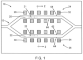
FIG. 1 is a top view of a structure at an initial fabrication stage of a processing method in accordance with embodiments of the invention. -
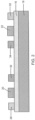
FIG. 2 is a cross-sectional view taken generally along line 2-2 inFIG. 1 . -
FIG. 3 is a top view of the structure at a fabrication stage subsequent toFIG. 2 . -
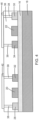
FIG. 4 is a cross-sectional view taken generally along line 4-4 inFIG. 3 . -
FIG. 4A is a cross-sectional view taken generally alongline 4A-4A inFIG. 3 . -
FIG. 4B is a cross-sectional view taken generally alongline 4B-4B inFIG. 3 . -
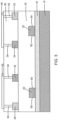
FIG. 5 is a cross-sectional view of a structure in accordance with alternative embodiments of the invention. -
FIGS. 6 ,6A ,6B are cross-sectional views of a structure in accordance with alternative embodiments of the invention. -
FIG. 7 is a top view of a structure in accordance with alternative embodiments of the invention. -
FIG. 7A is a cross-sectional view taken generally alongline 7A-7A inFIG. 7 . -
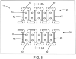
FIG. 8 is a top view of a structure in accordance with alternative embodiments of the invention. -
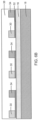
FIG. 8A is a cross-sectional view taken generally alongline 8A-8A inFIG. 8 . - With reference to
FIGS. 1 ,2 and in accordance with embodiments of the invention, astructure 10 includes awaveguide core 12 that is positioned on, and above, adielectric layer 16 and asemiconductor substrate 18. In an embodiment, thedielectric layer 16 may be comprised of a dielectric material, such as silicon dioxide, and thesemiconductor substrate 18 may be comprised of a semiconductor material, such as single-crystal silicon. In an embodiment, thedielectric layer 16 may be a buried oxide layer of a silicon-on-insulator substrate, and thedielectric layer 16 may separate thewaveguide core 12 from thesemiconductor substrate 18. - A portion of the
waveguide core 12 may configured to function as an optical phase shifter, such as a Mach-Zehnder modulator. In an embodiment, a portion of thewaveguide core 12 may be configured as a Mach-Zehnder modulator in which thewaveguide core 12 includes an arm orbranch 20 and an arm orbranch 22 that is positioned adjacent to, and laterally spaced from, thebranch 20. Thebranches waveguide core 12 are arranged between an input to the portion of thewaveguide core 12 and an output from the portion of thewaveguide core 12. Thebranches waveguide core 12 initially diverge away from each other at the input to the optical phase shifter into a divided light path. Thebranch 20 may include a portion aligned with alongitudinal axis 21, and thebranch 22 may include a portion aligned with alongitudinal axis 23. Thebranches branch 20 of thewaveguide core 12 may includeopposite sides branch 22 of thewaveguide core 12 may includeopposite sides side 60 of thebranch 20 may be positioned adjacent to theside 62 of thebranch 22. - In an embodiment, the
waveguide core 12 may be comprised of a material having a refractive index that is greater than the refractive index of silicon dioxide. In an embodiment, thewaveguide core 12 may be comprised of a semiconductor material. In an embodiment, thewaveguide core 12 may be comprised of single-crystal silicon. Thewaveguide core 12 may be formed by patterning a layer comprised of its constituent material with lithography and etching processes. In an embodiment, thewaveguide core 12 may be formed by patterning the semiconductor material (e.g., single-crystal silicon) of a device layer of a silicon-on-insulator substrate. In an alternative embodiment, thewaveguide core 12 may be comprised of a dielectric material, such as silicon nitride, silicon oxynitride, or aluminum nitride. - The
structure 10 may include athermoelectric device 24 that is associated with thebranch 20 of thewaveguide core 12. Thethermoelectric device 24 may include pillars orsections 28 of a thermoelectric material that alternate with pillars orsections 32 of a different thermoelectric material along the length of thebranch 20. In an embodiment, the thermoelectric material constituting thesections 28 may be a semiconductor material having an opposite conductivity type from the thermoelectric material constituting thesections 32. Thesections 28 and thesections 32 are disposed in a lateral direction transverse to thelongitudinal axis 22 on theopposite sides branch 20 of thewaveguide core 12. Each pair ofadjacent sections thermoelectric device 24. In an embodiment, thesections 28 and thesections 32 may be positioned directly on thedielectric layer 16. - In an embodiment, the
structure 10 may further include athermoelectric device 26 that is associated with thebranch 22 of thewaveguide core 12. Thethermoelectric device 26 includes pillars orsections 30 of a thermoelectric material and pillars orsection 34 of a different thermoelectric material that alternate with thesections 34 along the length of thebranch 22. In an embodiment, the thermoelectric material constituting thesections 30 may be a semiconductor material having an opposite conductivity type from the thermoelectric material constituting thesections 34. Thesections 30 and thesections 34 are disposed in a lateral direction transverse to thelongitudinal axis 23 on theopposite sides branch 22 of thewaveguide core 12. Each pair ofadjacent sections thermoelectric device 26. In an embodiment, thesections 30 and thesections 34 may be positioned directly on thedielectric layer 16. - In an embodiment, the
sections sections sections sections sections - In an embodiment, the
sections sections sections sections sections - With reference to
FIGS. 3 ,4 ,4A ,4B in which like reference numerals refer to like features inFIGS. 1 ,2 and at a subsequent fabrication stage, middle-of-line processing and back-end-of-line processing follow to form an interconnect structure that is coupled to thesections thermoelectric device 24 and that is coupled to thesections thermoelectric device 26. In particular, adielectric layer 36 may be formed on thewaveguide core 12, thesections thermoelectric device 24, and thesections thermoelectric device 26. Thewaveguide core 12, thesections thermoelectric device 24, and thesections thermoelectric device 26 are embedded in the dielectric material of thedielectric layer 36.Contacts 38 may be formed that extend through thedielectric layer 36 and land on thesections contacts 39 may be formed that extend through thedielectric layer 36 and land on thesections dielectric layer 36 may be comprised of a dielectric material, such as silicon dioxide, and thecontacts -
Interconnects 40 and interconnects 42 may be formed as top connectors over thedielectric layer 36 and, along with thecontacts sections thermoelectric device 24 in a series circuit. Theinterconnects 40 connect pairs ofadjacent sections side 58 or the side 60 (FIG. 1 ) of thebranch 20 of thewaveguide core 12 and may be lengthwise aligned parallel to the longitudinal axis 21 (FIG. 1 ) of thebranch 20. Theinterconnects 42 connect pairs ofadjacent sections opposite sides branch 20 of thewaveguide core 12 and may be extend across thebranch 20 transverse to thelongitudinal axis 21 of thewaveguide core 12. Theinterconnects 42 alternate with theinterconnects 40 such that thesections 28 and thesections 32 are connected in the series circuit. -
Interconnects 44 and interconnects 46 may be formed as top connectors over thedielectric layer 36 and, along with thecontacts sections thermoelectric device 26 in a series circuit. Theinterconnects 44 connect pairs ofadjacent sections side 62 or the side 64 (FIG. 1 ) of thebranch 22 of thewaveguide core 12 and may be lengthwise aligned parallel to the longitudinal axis 23 (FIG. 1 ) of thebranch 22. Theinterconnects 46 connect pairs ofadjacent sections opposite sides branch 22 of thewaveguide core 12 and may extend across thebranch 22 transverse to thelongitudinal axis 23 of thewaveguide core 12. Theinterconnects 46 alternate with theinterconnects 44 such that thesections 28 and thesections 32 are connected in the series circuit. - The
interconnects interconnects interconnects sections thermoelectric device 24 in the associated series circuit. Theinterconnects sections thermoelectric device 26 in the associated series circuit. - A
power supply 41 may have positive and negative terminals, as diagrammatically indicated inFIG. 3 , connected to the series circuit including theinterconnects sections thermoelectric device 24. Thepower supply 41 may supply a direct current to thethermoelectric device 24 with a current flow direction and a polarity that biases thethermoelectric device 24 to operate by the thermoelectric effect as a Peltier cooler. As a result, thethermoelectric device 24 may be used to extract heat from, and reduce the temperature of, thebranch 20 of thewaveguide core 12. The temperature reduction experienced by thebranch 20 of thewaveguide core 12 may result in a blue shift of the wavelength of the light propagating in thebranch 20 to a shorter wavelength than input into the optical phase shifter. The blue shift in wavelength increases with increasing power supplied from thepower supply 41 to thethermoelectric device 26 and the resulting lower temperature of thesections - A
power supply 45 may have positive and negative terminals, as diagrammatically indicated inFIG. 3 , connected to the series circuit including theinterconnects sections thermoelectric device 26. Thepower supply 45 may supply a direct current to thethermoelectric device 26 with a current flow direction and a polarity that biases thethermoelectric device 26 to operate by the thermoelectric effect as a Peltier heater. As a result, thethermoelectric device 26 may be used to supply heat to, and increase the temperature of, thebranch 20 of thewaveguide core 12. The temperature increase experienced by thebranch 22 of thewaveguide core 12 may result in a red shift of the wavelength of the light propagating in thebranch 22 to a longer wavelength than input into the optical phase shifter. The red shift in wavelength increases with increasing power supplied from thepower supply 45 to thethermoelectric device 26 and the resulting higher temperature of thesections - By cooling the
branch 20 of thewaveguide core 12 to provide a cold junction and heating thebranch 22 of thewaveguide core 12 to provide a hot junction, the wavelength differential for the phase shift effect of the optical phase shifter may be significantly increased without increasing the power consumption. In addition, the heat extracted by thethermoelectric device 24 to cool thebranch 20 may be offset by the heat generated by thethermoelectric device 26 to heat thebranch 22 such that thermal equilibrium may be maintained. Thermal stability may be achieved by the concurrent heating and cooling of thedifferent branches thermoelectric devices - In an alternative embodiment, only the
thermoelectric device 24 may be included in thestructure 10 and powered to either heat or cool the associatedbranch 20. In an alternative embodiment, only one or the other of thethermoelectric devices branch 20. In an alternative embodiment, both of thethermoelectric devices branches waveguide core 12 and cause a temperature decrease with associated blue shifting of the wavelength. In an alternative embodiment, both of thethermoelectric devices branches waveguide core 12 and cause a temperature increase with associated red shifting of the wavelength. - With reference to
FIG. 5 and in accordance with alternative embodiments, thesections thermoelectric device 24 and thesections thermoelectric device 26 may be spaced in a vertical direction above thebranches waveguide core 12 and arranged in a different level of thestructure 10 from thebranches waveguide core 12. Adielectric layer 35 may be formed on thewaveguide core 12, and thesections thermoelectric device 24 and thesections thermoelectric device 26 may be formed on thedielectric layer 35. Thewaveguide core 12 is embedded in the dielectric material of thedielectric layer 35. Thesections thermoelectric device 24 may have a non-overlapping relationship with thebranch 20 of thewaveguide core 12, and thesections thermoelectric device 26 may have a non-overlapping relationship with thebranch 22 of thewaveguide core 12. - With reference to
FIGS. 6 ,6A ,6B and in accordance with alternative embodiments, silicide layers 50 may be arranged in a vertical direction between thedielectric layer 16 and thesections thermoelectric device 24. Silicide layers 52 may be arranged in a vertical direction between thedielectric layer 16 and thesections thermoelectric device 26. The silicide layers 50, 52 may be formed by a silicidation process that involves one or more annealing steps to form a silicide phase by reacting a semiconductor material (e.g., the semiconductor material of the device layer of a silicon-on-insulator substrate) with a deposited layer comprised of a silicide-forming metal, such as nickel. The semiconductor material and/or the layer of silicide-forming metal may be patterned before silicidation to define a layout for the silicide layers 50, 52. An initial annealing step of the silicidation process may consume all or part of the silicide-forming metal to form the silicide layers 50, 52. Following the initial annealing step, any non-reacted silicide-forming metal may be removed by wet chemical etching. The silicide layers 50, 52 may then be subjected to an additional annealing step at a higher temperature to form a lower-resistance silicide phase. In an embodiment, the device layer of a silicon-on-insulator substrate may be fully silicided to form the silicide layers 50, 52. In an alternative embodiment, the device layer of a silicon-on-insulator substrate may be partially silicided to form the silicide layers 50, 52. - The
sections thermoelectric device 24 may be positioned on the silicide layers 50 such that the silicide layers 50 are disposed in a vertical direction between thedielectric layer 16 and thesections sections thermoelectric device 26 may be positioned on the silicide layers 52 such that the silicide layers 52 are disposed in a vertical direction between thedielectric layer 16 and thesections interconnects 40 and define bottom connectors between adjacent pairs of thesections thermoelectric device 24. Theinterconnects 42 provide top connectors in the series circuit including thesections interconnects 44 and define bottom connectors between adjacent pairs of thesections thermoelectric device 26. Theinterconnects 46 provide top connectors in the series circuit including thesections - With reference to
FIGS. 7 ,7A and in accordance with alternative embodiments, thestructure 10 may include a dopedregion 54 and a dopedregion 56 associated with each of thebranches waveguide core 12. The dopedregions regions waveguide core 12. In an embodiment, the semiconductor material of the dopedregion 54 may be doped with a p-type dopant (e.g., boron) that provides p-type electrical conductivity, and the semiconductor material of the dopedregion 56 may be doped with an n-type dopant (e.g., arsenic) that provides n-type electrical conductivity. - The
sections thermoelectric device 24 and thesections thermoelectric device 26, which are spaced in a vertical direction above thebranches waveguide core 12, may overlap with the dopedregions region 54 and in a portion of the dopedregion 56, and used to establish electrical contacts for biasing the optical phase shifter. In that regard,contacts 55 to the dopedregion 54 and the dopedregion 56 of thebranch 20 may be formed in the spaces between adjacent pairs of thesections thermoelectric device 24 that are not connected by theinterconnects 40. Similarly,contacts 57 to the dopedregion 54 and the dopedregion 56 of thebranch 22 may be formed in the spaces between adjacent pairs of thesections thermoelectric device 26 that are not connected by theinterconnects 42. - With reference to
FIGS. 8 ,8A and in accordance with alternative embodiments, thestructure 10 including the dopedregions sections thermoelectric device 24 on the silicide layers 50 and thesections thermoelectric device 26 on the silicide layers 52. The dopedregions branch 20 may be positioned in the same level as thesections sections regions branch 22 may be positioned in the same level as thesections sections contacts 55 to the dopedregions branch 20 may be located in spaces between thesections thermoelectric device 24 and thebranch 20 to avoid the bottom connections provided by the silicide layers 50. Thecontacts 57 to the dopedregions branch 22 may be located in spaces between thesections thermoelectric device 26 and thebranch 22 to avoid the bottom connections provided by the silicide layers 52. - The methods as described above are used in the fabrication of integrated circuit chips. The resulting integrated circuit chips can be distributed by the fabricator in raw wafer form (e.g., as a single wafer that has multiple unpackaged chips), as a bare die, or in a packaged form. The chip may be integrated with other chips, discrete circuit elements, and/or other signal processing devices as part of either an intermediate product or an end product. The end product can be any product that includes integrated circuit chips, such as computer products having a central processor or smartphones.
- References herein to terms modified by language of approximation, such as "about", "approximately", and "substantially", are not to be limited to the precise value specified. The language of approximation may correspond to the precision of an instrument used to measure the value and, unless otherwise dependent on the precision of the instrument, may indicate a range of +/- 10% of the stated value(s).
- References herein to terms such as "vertical", "horizontal", etc. are made by way of example, and not by way of limitation, to establish a frame of reference. The term "horizontal" as used herein is defined as a plane parallel to a conventional plane of a semiconductor substrate, regardless of its actual three-dimensional spatial orientation. The terms "vertical" and "normal" refer to a direction in the frame of reference perpendicular to the horizontal, as just defined. The term "lateral" refers to a direction in the frame of reference within the horizontal plane.
- A feature "connected" or "coupled" to or with another feature may be directly connected or coupled to or with the other feature or, instead, one or more intervening features may be present. A feature may be "directly connected" or "directly coupled" to or with another feature if intervening features are absent. A feature may be "indirectly connected" or "indirectly coupled" to or with another feature if at least one intervening feature is present. A feature "on" or "contacting" another feature may be directly on or in direct contact with the other feature or, instead, one or more intervening features may be present. A feature may be "directly on" or in "direct contact" with another feature if intervening features are absent. A feature may be "indirectly on" or in "indirect contact" with another feature if at least one intervening feature is present. Different features "overlap" if a feature extends over, and covers a part of, another feature.
- The descriptions of the various embodiments of the present invention have been presented for purposes of illustration but are not intended to be exhaustive or limited to the embodiments disclosed. Many modifications and variations will be apparent to those of ordinary skill in the art without departing from the scope and spirit of the described embodiments. The terminology used herein was chosen to best explain the principles of the embodiments, the practical application or technical improvement over technologies found in the marketplace, or to enable others of ordinary skill in the art to understand the embodiments disclosed herein.
Claims (15)
- A structure comprising:an optical phase shifter including a waveguide core having a first branch and a second branch laterally spaced from the first branch; anda first thermoelectric device including a first plurality of pillars and a second plurality of pillars that alternate with the first plurality of pillars in a first series circuit, the first plurality of pillars and the second plurality of pillars disposed adjacent to the first branch of the waveguide core, the first plurality of pillars comprising an n-type semiconductor material, and the second plurality of pillars comprising a p-type semiconductor material.
- The structure of claim 1 further comprising:
a second thermoelectric device including a first plurality of pillars and a second plurality of pillars that alternate with the first plurality of pillars in a second series circuit, the first plurality of pillars and the second plurality of pillars of the second thermoelectric device disposed adjacent to the second branch of the waveguide core, the first plurality of pillars comprising the n-type semiconductor material, and the second plurality of pillars comprising the p-type semiconductor material. - The structure of claim 1 or claim 2 further comprising:
a first power supply coupled to the first series circuit, the first power supply configured to supply a current to the first plurality of pillars and the second plurality of pillars of the first thermoelectric device to generate heat for elevating the temperature of the first branch of the waveguide core. - The structure of claim 2 or claim 3 further comprising:
a second power supply coupled to the second series circuit, the second power supply configured to supply a current to the first plurality of pillars and the second plurality of pillars of the second thermoelectric device to extract heat for cooling the second branch of the waveguide core. - The structure of one of claims 1 to 4 wherein the n-type semiconductor material comprises bismuth telluride, and the p-type semiconductor material comprises antimony telluride, or wherein the n-type semiconductor material comprises n-type silicon, and the p-type semiconductor material comprises p-type polycrystalline silicon or p-type polycrystalline silicon-germanium.
- The structure of claim 1 further comprising:
a power supply coupled to the first series circuit, the power supply configured to:supply a current to the first plurality of pillars and the second plurality of pillars to generate heat for elevating the temperature of the first branch of the waveguide core, orsupply a current to the first plurality of pillars and the second plurality of pillars to extract heat for cooling the first branch of the waveguide core. - The structure of one of claims 1 to 6 wherein the first plurality of pillars and the second plurality of pillars are arranged in a plurality of adjacent pairs, and further comprising:
a plurality of silicide layers, each silicide layer connecting one of the plurality of adjacent pairs of the first plurality of pillars and the second plurality of pillars. - The structure of claim 7 further comprising:a semiconductor substrate; anda dielectric layer on the semiconductor substrate,wherein the dielectric layer is positioned between the plurality of silicide layers and the semiconductor substrate, and/orwherein the plurality of silicide layers are positioned between the dielectric layer and the plurality of adjacent pairs of the first plurality of pillars and the second plurality of pillars.
- The structure of claim 7 or claim 8 wherein the waveguide core has a longitudinal axis, a first side, and a second side opposite from the first side, and the plurality of adjacent pairs of the first plurality of pillars and the second plurality of pillars are disposed along the longitudinal axis adjacent to the first side and the second side of the waveguide core.
- The structure of one of claims 1 to 9 further comprising:a dielectric layer on the waveguide core,wherein the waveguide core is embedded in the dielectric layer, and the first plurality of pillars and the second plurality of pillars are disposed on the dielectric layer over the first branch of the waveguide core.
- The structure of claim 10 wherein the optical phase shifter includes a first doped region and a second doped region, the waveguide core is positioned in a lateral direction between the first doped region and the second doped region, each of the first plurality of pillars overlaps with either the first doped region or the second doped region, and each of the second plurality of pillars overlaps with either the first doped region or the second doped region.
- The structure of one of claims 1 to 9 further comprising:a dielectric layer on the waveguide core, the first plurality of pillars, and the second plurality of pillars,wherein the waveguide core, the first plurality of pillars, and the second plurality of pillars are embedded in the dielectric layer.
- The structure of claim 12 wherein the optical phase shifter includes a first doped region and a second doped region, the first plurality of pillars and the second plurality of pillars are arranged in a plurality of adjacent pairs, and further comprising:
a plurality of silicide layers, each silicide layer connecting one of the plurality of adjacent pairs of the first plurality of pillars and the second plurality of pillars, and, optionally, wherein the first doped region and the second doped region are disposed in a lateral direction between the plurality of silicide layers and the waveguide core. - The structure of one of claims 1 to 9 further comprising:a semiconductor substrate; anda dielectric layer on the semiconductor substrate,wherein the dielectric layer is positioned between the first plurality of pillars and the semiconductor substrate, and the dielectric layer is positioned between the second plurality of pillars and the semiconductor substrate, and, optionally, wherein the first plurality of pillars and the second plurality of pillars are disposed directly on the dielectric layer.
- A method comprising:forming an optical phase shifter including a waveguide core having a first branch and a second branch laterally spaced from the first branch; andforming a thermoelectric device including a first plurality of pillars and a second plurality of pillars that alternate with the first plurality of pillars in a series circuit, wherein the first plurality of pillars and the second plurality of pillars are disposed adjacent to the first branch of the waveguide core, the first plurality of pillars comprise an n-type semiconductor material, and the second plurality of pillars comprise a p-type semiconductor material.
Applications Claiming Priority (1)
| Application Number | Priority Date | Filing Date | Title |
|---|---|---|---|
| US18/094,716 US12481196B2 (en) | 2023-01-09 | 2023-01-09 | Optical phase shifter with one or more integrated thermoelectric devices |
Publications (1)
| Publication Number | Publication Date |
|---|---|
| EP4398030A1 true EP4398030A1 (en) | 2024-07-10 |
Family
ID=88511508
Family Applications (1)
| Application Number | Title | Priority Date | Filing Date |
|---|---|---|---|
| EP23205376.9A Pending EP4398030A1 (en) | 2023-01-09 | 2023-10-24 | Optical phase shifter with one or more integrated thermoelectric devices |
Country Status (3)
| Country | Link |
|---|---|
| US (1) | US12481196B2 (en) |
| EP (1) | EP4398030A1 (en) |
| CN (1) | CN118311790A (en) |
Cited By (1)
| Publication number | Priority date | Publication date | Assignee | Title |
|---|---|---|---|---|
| CN119596570A (en) * | 2024-12-17 | 2025-03-11 | 武汉光谷信息光电子创新中心有限公司 | Phase shifter |
Families Citing this family (1)
| Publication number | Priority date | Publication date | Assignee | Title |
|---|---|---|---|---|
| US12701916B2 (en) * | 2022-05-20 | 2026-08-04 | Apple Inc. | Thermoelectric cooling modules |
Citations (3)
| Publication number | Priority date | Publication date | Assignee | Title |
|---|---|---|---|---|
| US6278822B1 (en) * | 1998-05-01 | 2001-08-21 | Bookham Technology Plc | Branched optical waveguide and its method of use |
| US20150147026A1 (en) * | 2013-11-27 | 2015-05-28 | Futurewei Technologies, Inc. | Apparatus and Method for Differential Thermal Optical Switch Control |
| US20220357629A1 (en) * | 2019-10-29 | 2022-11-10 | Nippon Telegraph And Telephone Corporation | Optical Module |
Family Cites Families (7)
| Publication number | Priority date | Publication date | Assignee | Title |
|---|---|---|---|---|
| US6825966B2 (en) * | 2001-11-13 | 2004-11-30 | International Business Machines Corporation | Optical phase shifting device |
| US6981380B2 (en) | 2002-12-20 | 2006-01-03 | Intel Corporation | Thermoelectric cooling for microelectronic packages and dice |
| US20130008479A1 (en) * | 2011-07-07 | 2013-01-10 | Peng Chen | Thermoelectric element design |
| FR3005755A1 (en) * | 2013-05-17 | 2014-11-21 | St Microelectronics Sa | DOUBLE STATIC ELECTRO-OPTICAL DEPTHASE WITH TWO CONTROL TERMINALS |
| US9684191B2 (en) * | 2015-11-05 | 2017-06-20 | International Business Machines Corporation | Efficient thermo-optic phase shifters using multi-pass heaters |
| KR102253397B1 (en) * | 2016-11-23 | 2021-05-20 | 한국전자통신연구원 | method for manufacturing optical switch and structure of the same |
| EP4338210A1 (en) * | 2021-05-10 | 2024-03-20 | European Thermodynamics Limited | Thermoelectric module |
-
2023
- 2023-01-09 US US18/094,716 patent/US12481196B2/en active Active
- 2023-10-24 EP EP23205376.9A patent/EP4398030A1/en active Pending
- 2023-10-27 CN CN202311408581.8A patent/CN118311790A/en active Pending
Patent Citations (3)
| Publication number | Priority date | Publication date | Assignee | Title |
|---|---|---|---|---|
| US6278822B1 (en) * | 1998-05-01 | 2001-08-21 | Bookham Technology Plc | Branched optical waveguide and its method of use |
| US20150147026A1 (en) * | 2013-11-27 | 2015-05-28 | Futurewei Technologies, Inc. | Apparatus and Method for Differential Thermal Optical Switch Control |
| US20220357629A1 (en) * | 2019-10-29 | 2022-11-10 | Nippon Telegraph And Telephone Corporation | Optical Module |
Cited By (1)
| Publication number | Priority date | Publication date | Assignee | Title |
|---|---|---|---|---|
| CN119596570A (en) * | 2024-12-17 | 2025-03-11 | 武汉光谷信息光电子创新中心有限公司 | Phase shifter |
Also Published As
| Publication number | Publication date |
|---|---|
| US20240231173A1 (en) | 2024-07-11 |
| US12481196B2 (en) | 2025-11-25 |
| CN118311790A (en) | 2024-07-09 |
Similar Documents
| Publication | Publication Date | Title |
|---|---|---|
| US10197819B2 (en) | Efficient thermo-optic phase shifters using multi-pass heaters | |
| US10509244B1 (en) | Optical switches and routers operated by phase-changing materials controlled by heaters | |
| US12481196B2 (en) | Optical phase shifter with one or more integrated thermoelectric devices | |
| US10996398B1 (en) | Switchable polarization splitters | |
| TW202101073A (en) | Integrated optoelectronic device with heater | |
| US11747556B2 (en) | Integrated circuit device including photoelectronic element | |
| US20140015089A1 (en) | Differential temperature sensor and its capacitors in cmos/bicmos technology | |
| US20030090775A1 (en) | Optical phase shifting device | |
| US10747030B1 (en) | Electro-optic modulators with stacked layers | |
| US11953723B2 (en) | Thermally tunable waveguide and photonic integrated circuit component having the same | |
| CN112666726B (en) | Thermo-optic phase shifter and preparation method thereof | |
| US12572050B2 (en) | Semiconductor device including optical ring waveguide | |
| US11287719B2 (en) | Tunable grating couplers containing a material with a variable refractive index | |
| EP4468070A1 (en) | Assisted thermo-optic phase shifters | |
| US10983412B1 (en) | Silicon photonic components fabricated using a bulk substrate | |
| US12293954B2 (en) | Method of fabricating semiconductor structure with heating element | |
| US12147074B2 (en) | Thermo-optic phase shifters | |
| US12601937B2 (en) | Thermo-optic phase shifters for a photonics chip | |
| US20260036835A1 (en) | Optical waveguide heater | |
| US12345919B2 (en) | Photonics chips with thermal management for a cavity-mounted chip | |
| US20260044027A1 (en) | Structures for a thermo-optic phase shifter | |
| US20240345320A1 (en) | Temperature adjustment element configured to improve modulation efficiency | |
| US20250344615A1 (en) | Phase-change device | |
| WO2024247010A1 (en) | Monitor circuit | |
| CN120085409A (en) | Optical device and manufacturing method |
Legal Events
| Date | Code | Title | Description |
|---|---|---|---|
| PUAI | Public reference made under article 153(3) epc to a published international application that has entered the european phase |
Free format text: ORIGINAL CODE: 0009012 |
|
| STAA | Information on the status of an ep patent application or granted ep patent |
Free format text: STATUS: THE APPLICATION HAS BEEN PUBLISHED |
|
| AK | Designated contracting states |
Kind code of ref document: A1 Designated state(s): AL AT BE BG CH CY CZ DE DK EE ES FI FR GB GR HR HU IE IS IT LI LT LU LV MC ME MK MT NL NO PL PT RO RS SE SI SK SM TR |
|
| STAA | Information on the status of an ep patent application or granted ep patent |
Free format text: STATUS: REQUEST FOR EXAMINATION WAS MADE |
|
| 17P | Request for examination filed |
Effective date: 20241030 |
|
| RBV | Designated contracting states (corrected) |
Designated state(s): AL AT BE BG CH CY CZ DE DK EE ES FI FR GB GR HR HU IE IS IT LI LT LU LV MC ME MK MT NL NO PL PT RO RS SE SI SK SM TR |