EP4398010A1 - Edge couplers with a fine-alignment mechanism - Google Patents
Edge couplers with a fine-alignment mechanism Download PDFInfo
- Publication number
- EP4398010A1 EP4398010A1 EP23204241.6A EP23204241A EP4398010A1 EP 4398010 A1 EP4398010 A1 EP 4398010A1 EP 23204241 A EP23204241 A EP 23204241A EP 4398010 A1 EP4398010 A1 EP 4398010A1
- Authority
- EP
- European Patent Office
- Prior art keywords
- waveguide core
- heater
- cavity
- dielectric layer
- gap
- Prior art date
- Legal status (The legal status is an assumption and is not a legal conclusion. Google has not performed a legal analysis and makes no representation as to the accuracy of the status listed.)
- Pending
Links
Images


Classifications
-
- G—PHYSICS
- G02—OPTICS
- G02B—OPTICAL ELEMENTS, SYSTEMS OR APPARATUS
- G02B6/00—Light guides; Structural details of arrangements comprising light guides and other optical elements, e.g. couplings
- G02B6/24—Coupling light guides
- G02B6/42—Coupling light guides with opto-electronic elements
- G02B6/4201—Packages, e.g. shape, construction, internal or external details
- G02B6/4266—Thermal aspects, temperature control or temperature monitoring
-
- G—PHYSICS
- G02—OPTICS
- G02B—OPTICAL ELEMENTS, SYSTEMS OR APPARATUS
- G02B6/00—Light guides; Structural details of arrangements comprising light guides and other optical elements, e.g. couplings
- G02B6/10—Light guides; Structural details of arrangements comprising light guides and other optical elements, e.g. couplings of the optical waveguide type
- G02B6/12—Light guides; Structural details of arrangements comprising light guides and other optical elements, e.g. couplings of the optical waveguide type of the integrated circuit kind
-
- G—PHYSICS
- G02—OPTICS
- G02B—OPTICAL ELEMENTS, SYSTEMS OR APPARATUS
- G02B6/00—Light guides; Structural details of arrangements comprising light guides and other optical elements, e.g. couplings
- G02B6/10—Light guides; Structural details of arrangements comprising light guides and other optical elements, e.g. couplings of the optical waveguide type
- G02B6/12—Light guides; Structural details of arrangements comprising light guides and other optical elements, e.g. couplings of the optical waveguide type of the integrated circuit kind
- G02B6/122—Basic optical elements, e.g. light-guiding paths
-
- G—PHYSICS
- G02—OPTICS
- G02B—OPTICAL ELEMENTS, SYSTEMS OR APPARATUS
- G02B6/00—Light guides; Structural details of arrangements comprising light guides and other optical elements, e.g. couplings
- G02B6/10—Light guides; Structural details of arrangements comprising light guides and other optical elements, e.g. couplings of the optical waveguide type
- G02B6/12—Light guides; Structural details of arrangements comprising light guides and other optical elements, e.g. couplings of the optical waveguide type of the integrated circuit kind
- G02B6/122—Basic optical elements, e.g. light-guiding paths
- G02B6/1228—Tapered waveguides, e.g. integrated spot-size transformers
-
- G—PHYSICS
- G02—OPTICS
- G02B—OPTICAL ELEMENTS, SYSTEMS OR APPARATUS
- G02B6/00—Light guides; Structural details of arrangements comprising light guides and other optical elements, e.g. couplings
- G02B6/10—Light guides; Structural details of arrangements comprising light guides and other optical elements, e.g. couplings of the optical waveguide type
- G02B6/12—Light guides; Structural details of arrangements comprising light guides and other optical elements, e.g. couplings of the optical waveguide type of the integrated circuit kind
- G02B6/13—Integrated optical circuits characterised by the manufacturing method
-
- G—PHYSICS
- G02—OPTICS
- G02B—OPTICAL ELEMENTS, SYSTEMS OR APPARATUS
- G02B6/00—Light guides; Structural details of arrangements comprising light guides and other optical elements, e.g. couplings
- G02B6/10—Light guides; Structural details of arrangements comprising light guides and other optical elements, e.g. couplings of the optical waveguide type
- G02B6/12—Light guides; Structural details of arrangements comprising light guides and other optical elements, e.g. couplings of the optical waveguide type of the integrated circuit kind
- G02B6/13—Integrated optical circuits characterised by the manufacturing method
- G02B6/132—Integrated optical circuits characterised by the manufacturing method by deposition of thin films
-
- G—PHYSICS
- G02—OPTICS
- G02B—OPTICAL ELEMENTS, SYSTEMS OR APPARATUS
- G02B6/00—Light guides; Structural details of arrangements comprising light guides and other optical elements, e.g. couplings
- G02B6/10—Light guides; Structural details of arrangements comprising light guides and other optical elements, e.g. couplings of the optical waveguide type
- G02B6/12—Light guides; Structural details of arrangements comprising light guides and other optical elements, e.g. couplings of the optical waveguide type of the integrated circuit kind
- G02B6/13—Integrated optical circuits characterised by the manufacturing method
- G02B6/136—Integrated optical circuits characterised by the manufacturing method by etching
-
- G—PHYSICS
- G02—OPTICS
- G02B—OPTICAL ELEMENTS, SYSTEMS OR APPARATUS
- G02B6/00—Light guides; Structural details of arrangements comprising light guides and other optical elements, e.g. couplings
- G02B6/24—Coupling light guides
- G02B6/26—Optical coupling means
- G02B6/30—Optical coupling means for use between fibre and thin-film device
- G02B6/305—Optical coupling means for use between fibre and thin-film device and having an integrated mode-size expanding section, e.g. tapered waveguide
-
- G—PHYSICS
- G02—OPTICS
- G02B—OPTICAL ELEMENTS, SYSTEMS OR APPARATUS
- G02B6/00—Light guides; Structural details of arrangements comprising light guides and other optical elements, e.g. couplings
- G02B6/24—Coupling light guides
- G02B6/26—Optical coupling means
- G02B6/35—Optical coupling means having switching means
- G02B6/3502—Optical coupling means having switching means involving direct waveguide displacement, e.g. cantilever type waveguide displacement involving waveguide bending, or displacing an interposed waveguide between stationary waveguides
-
- G—PHYSICS
- G02—OPTICS
- G02B—OPTICAL ELEMENTS, SYSTEMS OR APPARATUS
- G02B6/00—Light guides; Structural details of arrangements comprising light guides and other optical elements, e.g. couplings
- G02B6/24—Coupling light guides
- G02B6/26—Optical coupling means
- G02B6/35—Optical coupling means having switching means
- G02B6/3564—Mechanical details of the actuation mechanism associated with the moving element or mounting mechanism details
- G02B6/3566—Mechanical details of the actuation mechanism associated with the moving element or mounting mechanism details involving bending a beam, e.g. with cantilever
-
- G—PHYSICS
- G02—OPTICS
- G02B—OPTICAL ELEMENTS, SYSTEMS OR APPARATUS
- G02B6/00—Light guides; Structural details of arrangements comprising light guides and other optical elements, e.g. couplings
- G02B6/24—Coupling light guides
- G02B6/26—Optical coupling means
- G02B6/35—Optical coupling means having switching means
- G02B6/3564—Mechanical details of the actuation mechanism associated with the moving element or mounting mechanism details
- G02B6/3568—Mechanical details of the actuation mechanism associated with the moving element or mounting mechanism details characterised by the actuating force
- G02B6/3576—Temperature or heat actuation
-
- G—PHYSICS
- G02—OPTICS
- G02B—OPTICAL ELEMENTS, SYSTEMS OR APPARATUS
- G02B6/00—Light guides; Structural details of arrangements comprising light guides and other optical elements, e.g. couplings
- G02B6/24—Coupling light guides
- G02B6/26—Optical coupling means
- G02B6/35—Optical coupling means having switching means
- G02B6/3596—With planar waveguide arrangement, i.e. in a substrate, regardless if actuating mechanism is outside the substrate
-
- G—PHYSICS
- G02—OPTICS
- G02B—OPTICAL ELEMENTS, SYSTEMS OR APPARATUS
- G02B6/00—Light guides; Structural details of arrangements comprising light guides and other optical elements, e.g. couplings
- G02B6/24—Coupling light guides
- G02B6/42—Coupling light guides with opto-electronic elements
-
- G—PHYSICS
- G02—OPTICS
- G02B—OPTICAL ELEMENTS, SYSTEMS OR APPARATUS
- G02B6/00—Light guides; Structural details of arrangements comprising light guides and other optical elements, e.g. couplings
- G02B6/10—Light guides; Structural details of arrangements comprising light guides and other optical elements, e.g. couplings of the optical waveguide type
- G02B6/12—Light guides; Structural details of arrangements comprising light guides and other optical elements, e.g. couplings of the optical waveguide type of the integrated circuit kind
- G02B2006/12035—Materials
- G02B2006/12061—Silicon
-
- G—PHYSICS
- G02—OPTICS
- G02B—OPTICAL ELEMENTS, SYSTEMS OR APPARATUS
- G02B6/00—Light guides; Structural details of arrangements comprising light guides and other optical elements, e.g. couplings
- G02B6/10—Light guides; Structural details of arrangements comprising light guides and other optical elements, e.g. couplings of the optical waveguide type
- G02B6/12—Light guides; Structural details of arrangements comprising light guides and other optical elements, e.g. couplings of the optical waveguide type of the integrated circuit kind
- G02B2006/12083—Constructional arrangements
- G02B2006/12121—Laser
-
- G—PHYSICS
- G02—OPTICS
- G02B—OPTICAL ELEMENTS, SYSTEMS OR APPARATUS
- G02B6/00—Light guides; Structural details of arrangements comprising light guides and other optical elements, e.g. couplings
- G02B6/10—Light guides; Structural details of arrangements comprising light guides and other optical elements, e.g. couplings of the optical waveguide type
- G02B6/12—Light guides; Structural details of arrangements comprising light guides and other optical elements, e.g. couplings of the optical waveguide type of the integrated circuit kind
- G02B2006/12133—Functions
- G02B2006/12135—Temperature control
-
- G—PHYSICS
- G02—OPTICS
- G02B—OPTICAL ELEMENTS, SYSTEMS OR APPARATUS
- G02B6/00—Light guides; Structural details of arrangements comprising light guides and other optical elements, e.g. couplings
- G02B6/10—Light guides; Structural details of arrangements comprising light guides and other optical elements, e.g. couplings of the optical waveguide type
- G02B6/12—Light guides; Structural details of arrangements comprising light guides and other optical elements, e.g. couplings of the optical waveguide type of the integrated circuit kind
- G02B2006/12133—Functions
- G02B2006/12145—Switch
-
- G—PHYSICS
- G02—OPTICS
- G02B—OPTICAL ELEMENTS, SYSTEMS OR APPARATUS
- G02B6/00—Light guides; Structural details of arrangements comprising light guides and other optical elements, e.g. couplings
- G02B6/10—Light guides; Structural details of arrangements comprising light guides and other optical elements, e.g. couplings of the optical waveguide type
- G02B6/12—Light guides; Structural details of arrangements comprising light guides and other optical elements, e.g. couplings of the optical waveguide type of the integrated circuit kind
- G02B2006/12166—Manufacturing methods
- G02B2006/12176—Etching
-
- H—ELECTRICITY
- H01—ELECTRIC ELEMENTS
- H01S—DEVICES USING THE PROCESS OF LIGHT AMPLIFICATION BY STIMULATED EMISSION OF RADIATION [LASER] TO AMPLIFY OR GENERATE LIGHT; DEVICES USING STIMULATED EMISSION OF ELECTROMAGNETIC RADIATION IN WAVE RANGES OTHER THAN OPTICAL
- H01S5/00—Semiconductor lasers
- H01S5/02—Structural details or components not essential to laser action
- H01S5/022—Mountings; Housings
- H01S5/0235—Method for mounting laser chips
- H01S5/02375—Positioning of the laser chips
- H01S5/02385—Positioning of the laser chips using laser light as reference
Definitions
- An edge coupler also known as a spot-size converter, is an optical component that is commonly used for coupling light of a given mode from a light source, such as a laser or an optical fiber, to other optical components on the photonics chip.
- the edge coupler may include a section of a waveguide core that defines an inverse taper having a tip.
- the narrow end of the inverse taper provides a facet at the tip that is positioned adjacent to the light source, and the wide end of the inverse taper is connected to another section of the waveguide core that routes the light to the optical components of the photonics chip.
- the first heater may be positioned beneath the portion of the waveguide core.
- the structure may further comprise a second heater positioned in a lateral direction adjacent to the portion of the waveguide core. The second heater may be spaced by a second gap from the portion of the waveguide core.
- the laser chip 34 may be replaced by a different type of light source, such as an optical fiber, and the cavity 33 may have a compatible shape of a V-groove formed by an etching process characterized by an etch rate that varies with crystalline orientation.
- the alignment-adjustment mechanism of the structure 10 may modified to include another heater 25 that is positioned adjacent to the waveguide core 12. More specifically, the heater 25 may be positioned adjacent to the undercut portion 19 of the tapered section 18 of the waveguide core 12, and the undercut portion 19 of the tapered section 18 may be located in a lateral direction between the heater 24 and the heater 25. The heater 25 is separated from the undercut portion 19 of the tapered section 18 by a gap having a dimension D2.
- the heater 23 is separated in a vertical direction from the undercut portion 19 of the tapered section 18 by a gap that is filled by the dielectric material of the section of the dielectric layer 14.
- the dimension of the gap may be equal or substantially equal to the thickness of the dielectric layer 14.
- references herein to terms such as “vertical”, “horizontal”, etc. are made by way of example, and not by way of limitation, to establish a frame of reference.
- the term “horizontal” as used herein is defined as a plane parallel to a conventional plane of a semiconductor substrate, regardless of its actual three-dimensional spatial orientation.
- the terms “vertical” and “normal” refer to a direction in the frame of reference perpendicular to the horizontal, as just defined.
- the term “lateral” refers to a direction in the frame of reference within the horizontal plane.
Landscapes
- Physics & Mathematics (AREA)
- General Physics & Mathematics (AREA)
- Optics & Photonics (AREA)
- Engineering & Computer Science (AREA)
- Microelectronics & Electronic Packaging (AREA)
- Power Engineering (AREA)
- Optical Integrated Circuits (AREA)
Abstract
Description
- The disclosure relates to photonics chips and, more specifically, to structures including an edge coupler and methods of forming such structures.
- Photonics chips are used in many applications and systems including, but not limited to, data communication systems and data computation systems. A photonics chip integrates optical components and electronic components into a unified platform. Among other factors, layout area, cost, and operational overhead may be reduced by the integration of both types of components on the same chip.
- An edge coupler, also known as a spot-size converter, is an optical component that is commonly used for coupling light of a given mode from a light source, such as a laser or an optical fiber, to other optical components on the photonics chip. The edge coupler may include a section of a waveguide core that defines an inverse taper having a tip. In the edge coupler construction, the narrow end of the inverse taper provides a facet at the tip that is positioned adjacent to the light source, and the wide end of the inverse taper is connected to another section of the waveguide core that routes the light to the optical components of the photonics chip.
- The gradually-varying cross-sectional area of the inverse taper supports mode transformation and mode size variation associated with mode conversion when light is transferred from the light source to the edge coupler. The tip of the inverse taper is unable to fully confine the incident mode received from the light source because the cross-sectional area of the tip is considerably smaller than the mode size. Consequently, a significant percentage of the electromagnetic field of the incident mode is distributed about the tip of the inverse taper. As its width increases, the inverse taper can support the entire incident mode and confine the electromagnetic field.
- Improved structures including an edge coupler and methods of forming such structures are needed.
- In an embodiment of the invention, a structure comprises a dielectric layer on a semiconductor substrate. The dielectric layer includes a cavity and an edge defining a boundary of the cavity. The structure further comprises an edge coupler including a waveguide core. The waveguide core includes a portion that extends past the edge of the dielectric layer and overhangs the cavity. The structure further comprises a heater positioned adjacent to the portion of the waveguide core. The heater is spaced by a gap from the portion of the waveguide core.
- The first heater may be positioned in a lateral direction adjacent to the portion of the waveguide core. Moreover, the first heater may be positioned on the first dielectric layer. Additionally, the first heater may be disposed at least in part over the first cavity. Alternatively, the first heater may be fully disposed over the first cavity. Independent of the specific details of the arrangement of the first heater, the first heater may be configured to expand in dimensions in response to being powered such that the portion of the waveguide core bends relative to a light output.
- According to a further development, the structure may additionally comprise a second heater positioned in the lateral direction adjacent to the portion of the waveguide core. The second heater may be spaced by a second gap from the portion of the waveguide core. Optionally, the second gap may be equal to the first gap. Moreover, the first heater and the second heater may each be positioned at least in part over the first cavity. Additionally or alternatively, the first heater and the second heater may each be positioned on the first dielectric layer.
- Additionally or alternatively, the waveguide core of the structure may have an end surface, and the structure may further comprise a light source positioned adjacent to the end surface of the waveguide core. The light source may have a light output configured to provide light in a mode propagation direction toward the waveguide core. The light source may be a laser chip that includes a semiconductor laser.
- Additionally or alternatively, the structure may further comprise a second dielectric layer over the waveguide core and the first heater. The second dielectric layer may comprise a dielectric material, and the dielectric material may be disposed in the first gap between the first heater and the waveguide core.
- According to another variant, the first heater may be positioned beneath the portion of the waveguide core. According to this variant, the structure may further comprise a second heater positioned in a lateral direction adjacent to the portion of the waveguide core. The second heater may be spaced by a second gap from the portion of the waveguide core.
- Independent of the above-mentioned implementation details, the semiconductor substrate may further include a second cavity disposed beneath the first cavity and the portion of the waveguide core. The second cavity may adjoin the first cavity.
- Additionally, the portion of the waveguide core may be a tapered section. Further, the waveguide core may comprise single-crystal silicon or polysilicon, and the first heater may comprise tungsten.
- In an embodiment of the invention, a method comprises forming a cavity in a dielectric layer that is disposed on a semiconductor substrate. The dielectric layer includes an edge defining a boundary of the cavity. The method further comprises forming an edge coupler including a waveguide core. The waveguide core includes a portion that extends past the edge of the dielectric layer and overhangs the cavity. The method further comprises forming a heater positioned in a lateral direction adjacent to the portion of the waveguide core. The heater is spaced by a gap from the portion of the waveguide core.
- The accompanying drawings, which are incorporated in and constitute a part of this specification, illustrate various embodiments of the invention and, together with a general description of the invention given above and the detailed description of the embodiments given below, serve to explain the embodiments of the invention. In the drawings, like reference numerals refer to like features in the various views.
-
FIG. 1 is a top view of a structure at an initial fabrication stage of a processing method in accordance with embodiments of the invention. -
FIG. 2 is a cross-sectional view taken generally along line 2-2 inFIG. 1 . -
FIG. 2A is a cross-sectional view taken generally alongline 2A-2A inFIG. 1 . -
FIGS. 3, 3A are cross-sectional views of the structure at a fabrication stage of the processing method subsequent toFIGS. 2 ,2A . -
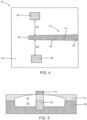
FIG. 4 is a top view of a structure in accordance with alternative embodiments of the invention. -
FIG. 5 is a cross-sectional view of a structure in accordance with alternative embodiments of the invention. - With reference to
FIGS. 1, 2 ,2A and in accordance with embodiments of the invention, astructure 10 for an edge coupler includes awaveguide core 12 that is positioned over adielectric layer 14 and asemiconductor substrate 16. In an embodiment, thedielectric layer 14 may be comprised of a dielectric material, such as silicon dioxide, and thesemiconductor substrate 16 may be comprised of a semiconductor material, such as single-crystal silicon. In an embodiment, thedielectric layer 14 may be a buried oxide layer of a silicon-on-insulator substrate, and thedielectric layer 14 may fully separate thewaveguide core 12 from thesemiconductor substrate 16. In an alternative embodiment, one or more additional dielectric layers comprised of, for example, silicon dioxide may be positioned between thewaveguide core 12 and thedielectric layer 14. - The
waveguide core 12 may include atapered section 18, asection 20 connected to thetapered section 18, and anend surface 22 that terminates thetapered section 18. Thetapered section 18 and thesection 20 of thewaveguide core 12 may be aligned along alongitudinal axis 21. The taperedsection 18 may increase in width with increasing distance along thelongitudinal axis 21 from theend surface 22. Thesection 20 of thewaveguide core 12 may be connected to other optical components. In an alternative embodiment, another tapered section with a different taper angle may be adjoined to the taperedsection 18 to define a compound taper. In embodiments, thewaveguide core 12 may have a width of about 500 nanometers to 1000 nanometers and a height of about 500 nanometers to 1000 nanometers. - In an embodiment, the
waveguide core 12 may be comprised of a material having a refractive index that is greater than the refractive index of silicon dioxide. In an embodiment, thewaveguide core 12 may be comprised of a semiconductor material, such as single-crystal silicon or polysilicon. In an embodiment, thewaveguide core 12 may be formed by patterning a layer comprised of the constituent material with lithography and etching processes. In an embodiment, an etch mask may be formed by a lithography process over a layer of the constituent material, and unmasked sections of the layer may be etched by an etching process. The shape of the etch mask determines the patterned shape of thewaveguide core 12. In an embodiment, thewaveguide core 12 may be formed by patterning the semiconductor material (e.g., single-crystal silicon) of a device layer of a silicon-on-insulator substrate. In an embodiment, thewaveguide core 12 may be formed by depositing a layer comprised of the constituent material (e.g., polysilicon) and patterning the deposited layer. - The
structure 10 may include an alignment-adjustment mechanism in the form of aheater 24 that is positioned adjacent to thewaveguide core 12. More specifically, theheater 24 may be positioned adjacent to the taperedsection 18 of thewaveguide core 12 and spaced from the taperedsection 18. Theheater 24 may be separated from the taperedsection 18 of thewaveguide core 12 by a gap having a dimension D1. Theheater 24 may be comprised of a metal, such as tungsten, that is deposited and patterned to shape by lithography and etching processes. Alternatively, theheater 24 may be comprised of a different metal that is also characterized by a similarly high coefficient of thermal expansion. In an embodiment, theheater 24 may have a width on the order of 50 microns and a length on the order of 300 microns, and the dimension D1 may range from about 2 microns to about 3 microns. - With reference to
FIGS. 3, 3A in which like reference numerals refer to like features inFIGS. 2 ,2A and at a subsequent fabrication stage, adielectric layer 26 may be formed over thewaveguide core 12 andheater 24. Thedielectric layer 26 may be comprised of a dielectric material, such as silicon dioxide, having a refractive index that is less than the refractive index of the material constituting thewaveguide core 12. Thedielectric layer 26 may be deposited and planarized following deposition. Portions of thedielectric layer 26 fill the gap between theheater 24 and thewaveguide core 12 with dielectric material. -
Contacts 28, which are formed in thedielectric layer 26, may be physically and electrically connected to theheater 24. Thecontacts 28 may be comprised of a metal, such as tungsten, that is deposited in openings patterned in thedielectric layer 26. Thecontacts 28 may connect theheater 24 with apower source 30 that can be operated to supply a current that causes Joule heating of theheater 24 such that theheater 24 can expand in size with the temperature increase. - A
cavity 32 may be formed in thedielectric layer 14, and acavity 33 may be formed in thesemiconductor substrate 16. Thecavity 33 may be formed in thesemiconductor substrate 16 by one or more wet etching processes. Thecavity 32 may be formed by a wet etching process that is performed following the formation of thecavity 33, and thecavities cavity 33 is arranged between thecavity 32 and thesemiconductor substrate 16. Thedielectric layer 14 has anedge 35 that borders thecavity 32 and thereby defines a boundary of thecavity 32 that is located beneath an undercutportion 19 of the taperedsection 18 of thewaveguide core 12. The undercutportion 19 of the taperedsection 18 of thewaveguide core 12 extends past theedge 35 of thedielectric layer 14 and overhangs thecavities edge 35 of thedielectric layer 14. In an embodiment, the overhang distance of the undercutportion 19 of the taperedsection 18 relative to theedge 35 may be approximately two microns. - In an embodiment, at least a portion of the bottom surface of the undercut
portion 19 ofwaveguide core 12 may adjoin thecavity 32. Thecavity 32, which communicates with thecavity 33, relaxes the mechanical constraint imposed on the undercutportion 19 of the taperedsection 18 of thewaveguide core 12. Theheater 24 is disposed on thedielectric layer 14. In an embodiment, theheater 24 may be disposed on thedielectric layer 14 at least in part over thecavity 32. In an embodiment, theheater 24 may be disposed on thedielectric layer 14 fully over thecavity 32. - A
laser chip 34 may be disposed inside thecavity 33. The shape and dimensions of thecavity 33 may be correlated with the shape and dimensions of thelaser chip 34 such that thelaser chip 34 can be inserted into thecavity 33. In that regard, the dimensions of thecavity 33 may be slightly greater than the dimensions of thelaser chip 34 to provide clearance for insertion into thecavity 33. Theend surface 22 of the taperedsection 18 of thewaveguide core 12 may be positioned adjacent to anoutput 36 for laser light from thelaser chip 34. In an embodiment, theoutput 36 from thelaser chip 34 may be aligned with theend surface 22 of the taperedsection 18 of thewaveguide core 12. In an alternative embodiment, thelaser chip 34 may be replaced by a different type of light source, such as a semiconductor optical amplifier. In an alternative embodiment, thelaser chip 34 may be replaced by a different type of light source, such as an optical fiber, and thecavity 33 may have a compatible shape of a V-groove formed by an etching process characterized by an etch rate that varies with crystalline orientation. - In an embodiment, the
laser chip 34 may be a hybrid laser that is configured to emit laser light of a given wavelength, intensity, mode shape, and mode size. In an embodiment, thelaser chip 34 may include a laser comprised of III-V compound semiconductor materials. In an embodiment, thelaser chip 34 may include an indium phosphide/indium-gallium-arsenic phosphide laser that is configured to generate continuous laser light in an infrared wavelength range for emission from theoutput 36. For example, the laser included in thelaser chip 34 may generate and output laser light from theoutput 36 at a nominal peak wavelength of 1310 nm or at a nominal peak wavelength of 1550 nm. - The
laser chip 34 may have the form of a flip-chip package that is externally assembled and attached to the photonics chip by solder balls or bumps to provide a fixed position. The flip-chip attachment process may include inserting thelaser chip 34 into thecavity 33 and reflowing the solder in the solder balls or bumps. Thelaser chip 34 may contact with the mechanical stops, after attachment, that provide passive alignment of the attachedlaser chip 34 in a vertical direction. In an embodiment, the taperedsection 18 of thewaveguide core 12 may be longitudinally aligned with the light emitted from theoutput 36 from thelaser chip 34. Following assembly by flip-chip attachment, the position of thelaser chip 34 is fixed. - In use, laser light may be supplied from the
output 36 of thelaser chip 34 to the taperedsection 18 ofwaveguide core 12. Thepower source 30 is operated to supply a current to theheater 24 that causes Joule heating of theheater 24, which expands in size due to the temperature increase and positive coefficient of thermal expansion. The thermal expansion in size or dimensions of theheater 24 is transferred through thedielectric layer 26 to the undercutportion 19 of the taperedsection 18 of thewaveguide core 12. The undercutportion 19 of the taperedsection 18 of thewaveguide core 12 may bend in a lateral direction, as diagrammatically shown by the double-headedarrow 40. The bending of the undercutportion 19 of the taperedsection 18 of thewaveguide core 12 may be used to adjust the lateral alignment of theoutput 36 of thelaser chip 34 with theend surface 22 of thewaveguide core 12. In an embodiment, the lateral bending may reposition theend surface 22 in a lateral direction by a distance of less than or equal to one micron. Alogic feedback loop 38 may be used to adjust the lateral position of the undercutportion 19 of the taperedsection 18 of thewaveguide core 12 for maximizing the laser power input to the edge coupler during the alignment process. Thelogic feedback loop 38, which is coupled to thepower source 30, may sample the laser power using an on-chip photodetector, as the position is adjusted, and provide control signals to thepower source 30 for changing the current supplied to theheater 24. Theheater 24 responds to the associated temperature change by changing its dimensions. In an embodiment, thelaser chip 34 may be intentionally misaligned when mounted inside thecavity 33 during assembly, and current may be continuously supplied from thepower source 30 to theheater 24 in order to provide a constant amount of lateral bending that corrects the intentional misalignment. - The alignment mechanism provides active fine-alignment adjustment that overcomes an inability to adjust the alignment of the
output 36 of thelaser chip 34 with thewaveguide core 12 due to the fixed post-assembly position of thelaser chip 34 inside thecavity 33. For example, misalignment that occurs due to aging during post-assembly operation may be compensated by changing the current supplied from thepower source 30 to theheater 24 such that the lateral bending of the taperedsection 18 of thewaveguide core 12 is altered. - With reference to
FIG. 4 and in accordance with alternative embodiments, the alignment-adjustment mechanism of thestructure 10 may modified to include anotherheater 25 that is positioned adjacent to thewaveguide core 12. More specifically, theheater 25 may be positioned adjacent to the undercutportion 19 of the taperedsection 18 of thewaveguide core 12, and the undercutportion 19 of the taperedsection 18 may be located in a lateral direction between theheater 24 and theheater 25. Theheater 25 is separated from the undercutportion 19 of the taperedsection 18 by a gap having a dimension D2. In an embodiment, the dimension D2 of the gap between the undercutportion 19 of the taperedsection 18 and theheater 25 may be equal to the dimension D1 of the gap between the undercutportion 19 of the taperedsection 18 and theheater 24 such that theheaters portion 19 of the taperedsection 18. Theheater 25 may be comprised of a metal, such as tungsten, that is deposited and patterned by lithography and etching processes. Theheater 25 may be disposed on thedielectric layer 14 and at least in part over thecavity 32. - With reference to
FIG. 5 and in accordance with alternative embodiments, aheater 23 similar to theheaters portion 19 of the taperedsection 18 of thewaveguide core 12. In particular, theheater 23 may be disposed in thecavity 33 in thesemiconductor substrate 16 and located beneath the undercutportion 19 of the taperedsection 18. A section of thedielectric layer 14 may be disposed in a vertical direction between theheater 23 and the undercutportion 19 of the taperedsection 18. The section of thedielectric layer 14, which is disposed in thecavity 32, may extend from theedge 35 parallel to thelongitudinal axis 21 of thewaveguide core 12 and beneath the undercutportion 19 of the taperedsection 18. Theheater 23 is separated in a vertical direction from the undercutportion 19 of the taperedsection 18 by a gap that is filled by the dielectric material of the section of thedielectric layer 14. In an embodiment, the dimension of the gap may be equal or substantially equal to the thickness of thedielectric layer 14. - The
heater 23, upon dimensional expansion from a temperature increase induced by heating, may be operative to bend the undercutportion 19 of the taperedsection 18. In an embodiment, the bending due to the thermal expansion of the size of theheater 23 may primarily include a vertical component. Theheater 23 may be used in combination with theheater 24, in combination with bothheaters output 36 of thelaser chip 34 with theend surface 22 of the taperedsection 18 of thewaveguide core 12. - The methods as described above are used in the fabrication of integrated circuit chips. The resulting integrated circuit chips can be distributed by the fabricator in raw wafer form (e.g., as a single wafer that has multiple unpackaged chips), as a bare die, or in a packaged form. The chip may be integrated with other chips, discrete circuit elements, and/or other signal processing devices as part of either an intermediate product or an end product. The end product can be any product that includes integrated circuit chips, such as computer products having a central processor or smartphones.
- References herein to terms modified by language of approximation, such as "about", "approximately", and "substantially", are not to be limited to the precise value specified. The language of approximation may correspond to the precision of an instrument used to measure the value and, unless otherwise dependent on the precision of the instrument, may indicate a range of +/- 10% of the stated value(s).
- References herein to terms such as "vertical", "horizontal", etc. are made by way of example, and not by way of limitation, to establish a frame of reference. The term "horizontal" as used herein is defined as a plane parallel to a conventional plane of a semiconductor substrate, regardless of its actual three-dimensional spatial orientation. The terms "vertical" and "normal" refer to a direction in the frame of reference perpendicular to the horizontal, as just defined. The term "lateral" refers to a direction in the frame of reference within the horizontal plane.
- A feature "connected" or "coupled" to or with another feature may be directly connected or coupled to or with the other feature or, instead, one or more intervening features may be present. A feature may be "directly connected" or "directly coupled" to or with another feature if intervening features are absent. A feature may be "indirectly connected" or "indirectly coupled" to or with another feature if at least one intervening feature is present. A feature "on" or "contacting" another feature may be directly on or in direct contact with the other feature or, instead, one or more intervening features may be present. A feature may be "directly on" or in "direct contact" with another feature if intervening features are absent. A feature may be "indirectly on" or in "indirect contact" with another feature if at least one intervening feature is present. Different features "overlap" if a feature extends over, and covers a part of, another feature.
- The descriptions of the various embodiments of the present invention have been presented for purposes of illustration but are not intended to be exhaustive or limited to the embodiments disclosed. Many modifications and variations will be apparent to those of ordinary skill in the art without departing from the scope and spirit of the described embodiments. The terminology used herein was chosen to best explain the principles of the embodiments, the practical application or technical improvement over technologies found in the marketplace, or to enable others of ordinary skill in the art to understand the embodiments disclosed herein.
Claims (15)
- A structure comprising:a semiconductor substrate;a first dielectric layer on the semiconductor substrate, the first dielectric layer including a first cavity and an edge defining a boundary of the first cavity;an edge coupler including a waveguide core, the waveguide core including a portion that extends past the edge of the first dielectric layer and overhangs the first cavity; anda first heater positioned adjacent to the portion of the waveguide core, the first heater spaced by a first gap from the portion of the waveguide core.
- The structure of claim 1 wherein the first heater is positioned in a lateral direction adjacent to the portion of the waveguide core.
- The structure of claim 2 further comprising:
a second heater positioned in the lateral direction adjacent to the portion of the waveguide core, the second heater spaced by a second gap from the portion of the waveguide core, and, optionally, wherein the second gap is equal to the first gap. - The structure of claim 3 wherein the first heater and the second heater are each positioned at least in part over the first cavity, and/or wherein the first heater and the second heater are each positioned on the first dielectric layer.
- The structure of one of claims 1 to 4 wherein the waveguide core has an end surface, and further comprising:
a light source positioned adjacent to the end surface of the waveguide core, the light source having a light output configured to provide light in a mode propagation direction toward the waveguide core, and, optionally, wherein the light source is a laser chip that includes a semiconductor laser. - The structure of one of claims 1 to 5 wherein the first heater is configured to expand in dimensions in response to being powered such that the portion of the waveguide core bends relative to a light output.
- The structure of one of claims 1 to 6 further comprising:
a second dielectric layer over the waveguide core and the first heater, the second dielectric layer comprising a dielectric material, and the dielectric material disposed in the first gap between the first heater and the waveguide core. - The structure of one of claims 1 to 7 wherein the first heater is disposed at least in part over the first cavity, or wherein the first heater is fully disposed over the first cavity.
- The structure of one of claims 1 to 8 wherein the first heater is positioned on the first dielectric layer.
- The structure of claim 1 wherein the first heater is positioned beneath the portion of the waveguide core.
- The structure of claim 10 further comprising:
a second heater positioned in a lateral direction adjacent to the portion of the waveguide core, the second heater spaced by a second gap from the portion of the waveguide core. - The structure of one of claims 1 to 11 wherein the semiconductor substrate includes a second cavity disposed beneath the first cavity and the portion of the waveguide core, and, optionally, wherein the second cavity adjoins the first cavity.
- The structure of one of claims 1 to 12 wherein the portion of the waveguide core is a tapered section.
- The structure of one of claims 1 to 13 wherein the waveguide core comprises single-crystal silicon or polysilicon, and the first heater comprises tungsten.
- A method comprising:forming a cavity in a dielectric layer that is disposed on a semiconductor substrate, wherein the dielectric layer includes an edge defining a boundary of the cavity;forming an edge coupler including a waveguide core, wherein the waveguide core includes a portion that extends past the edge of the dielectric layer and overhangs the cavity; andforming a heater positioned in a lateral direction adjacent to the portion of the waveguide core, wherein the heater is spaced by a gap from the portion of the waveguide core.
Applications Claiming Priority (1)
| Application Number | Priority Date | Filing Date | Title |
|---|---|---|---|
| US18/093,039 US12339494B2 (en) | 2023-01-04 | 2023-01-04 | Edge couplers with a fine-alignment mechanism |
Publications (1)
| Publication Number | Publication Date |
|---|---|
| EP4398010A1 true EP4398010A1 (en) | 2024-07-10 |
Family
ID=88417040
Family Applications (1)
| Application Number | Title | Priority Date | Filing Date |
|---|---|---|---|
| EP23204241.6A Pending EP4398010A1 (en) | 2023-01-04 | 2023-10-18 | Edge couplers with a fine-alignment mechanism |
Country Status (3)
| Country | Link |
|---|---|
| US (1) | US12339494B2 (en) |
| EP (1) | EP4398010A1 (en) |
| CN (1) | CN118295084A (en) |
Families Citing this family (1)
| Publication number | Priority date | Publication date | Assignee | Title |
|---|---|---|---|---|
| US20260153758A1 (en) * | 2024-12-03 | 2026-06-04 | Tower Semiconductor Ltd. | Photonic integrated circuit and methods related to the photonic integrated circuit |
Citations (5)
| Publication number | Priority date | Publication date | Assignee | Title |
|---|---|---|---|---|
| US20040184710A1 (en) * | 2003-03-19 | 2004-09-23 | Xerox Corporation | MEMS optical latching switch |
| US20050167508A1 (en) * | 2002-06-07 | 2005-08-04 | Richard Syms | Microengineered optical scanner |
| WO2010082524A1 (en) * | 2009-01-13 | 2010-07-22 | 日本電気株式会社 | Optical functional integrated device |
| US20190369328A1 (en) * | 2016-09-29 | 2019-12-05 | Oclaro Technology Limited | Waveguide Structure |
| US11320718B1 (en) * | 2019-09-26 | 2022-05-03 | Apple Inc. | Cantilever beam waveguide for silicon photonics device |
Family Cites Families (2)
| Publication number | Priority date | Publication date | Assignee | Title |
|---|---|---|---|---|
| US6559464B1 (en) | 1999-11-15 | 2003-05-06 | Axsun Technologies, Inc. | Optical system active alignment process including alignment structure attach, position search, and deformation |
| US10895702B2 (en) | 2019-04-01 | 2021-01-19 | Google Llc | Integrated heater structures in a photonic integrated circuit for solder attachment applications |
-
2023
- 2023-01-04 US US18/093,039 patent/US12339494B2/en active Active
- 2023-10-18 EP EP23204241.6A patent/EP4398010A1/en active Pending
- 2023-10-30 CN CN202311423352.3A patent/CN118295084A/en active Pending
Patent Citations (5)
| Publication number | Priority date | Publication date | Assignee | Title |
|---|---|---|---|---|
| US20050167508A1 (en) * | 2002-06-07 | 2005-08-04 | Richard Syms | Microengineered optical scanner |
| US20040184710A1 (en) * | 2003-03-19 | 2004-09-23 | Xerox Corporation | MEMS optical latching switch |
| WO2010082524A1 (en) * | 2009-01-13 | 2010-07-22 | 日本電気株式会社 | Optical functional integrated device |
| US20190369328A1 (en) * | 2016-09-29 | 2019-12-05 | Oclaro Technology Limited | Waveguide Structure |
| US11320718B1 (en) * | 2019-09-26 | 2022-05-03 | Apple Inc. | Cantilever beam waveguide for silicon photonics device |
Non-Patent Citations (2)
| Title |
|---|
| PETERS TJITTE-JELTE ET AL: "Electrothermal Actuators for SiO2 Photonic MEMS", vol. 7, no. 11, 7 November 2016 (2016-11-07), pages 200, XP093144506, ISSN: 2072-666X, Retrieved from the Internet <URL:https://pure.tudelft.nl/ws/portalfiles/portal/8089350/micromachines_07_00200_v2.pdf> DOI: 10.3390/mi7110200 * |
| SHARMA SURAJ ET AL: "Integrated 1?x?3 MEMS silicon nitride photonics switch", OPTICS EXPRESS, vol. 30, no. 12, 6 June 2022 (2022-06-06), US, pages 22200, XP093145083, ISSN: 1094-4087, DOI: 10.1364/OE.460533 * |
Also Published As
| Publication number | Publication date |
|---|---|
| US12339494B2 (en) | 2025-06-24 |
| CN118295084A (en) | 2024-07-05 |
| US20240219636A1 (en) | 2024-07-04 |
Similar Documents
| Publication | Publication Date | Title |
|---|---|---|
| US11531164B2 (en) | Hybrid edge couplers with layers in multiple levels | |
| US11366269B2 (en) | Edge couplers with a partially-etched inverse taper | |
| US6888989B1 (en) | Photonic chip mounting in a recess for waveguide alignment and connection | |
| JP2021513667A (en) | Integrated active device with improved optical coupling to dielectric waveguide | |
| US11822120B2 (en) | Optical components with enhanced heat dissipation | |
| CN104766903A (en) | Integrated module and forming method thereof | |
| JPH0875957A (en) | Optical Waveguide Combined with Photon Device | |
| US12147075B2 (en) | Back-end-of-line edge couplers with a tapered grating | |
| WO2015063628A1 (en) | Photonic circuit device with on-chip optical gain measurement structures | |
| US20070286552A1 (en) | Structure Comprising An Adiabatic Coupler For Adiabatic Coupling Of Light Between Two Optical Waveguides And Method For Manufacturing Such A Structure | |
| US20240061176A1 (en) | Structures for an optical coupler and related methods | |
| CN116661062A (en) | Integrated GaAs active devices with improved optical coupling to dielectric waveguides | |
| US12444906B2 (en) | Heterogeneously integrated photonic platform with improved thermal performance | |
| US12339494B2 (en) | Edge couplers with a fine-alignment mechanism | |
| US11409040B1 (en) | Optical couplers for ridge-to-rib waveguide core transitions | |
| US12117648B2 (en) | Hybrid integration method | |
| Kapulainen et al. | Hybrid integration of InP lasers with SOI waveguides using thermocompression bonding | |
| US11892680B2 (en) | Edge couplers with a high-elevation assistance feature | |
| EP4443672A2 (en) | Heterogeneous lasers with facets optimized for high power | |
| US12038610B2 (en) | Wafer-level optoelectronic packaging | |
| US11982850B2 (en) | Optical micro-electromechanical system with flip chip packaging | |
| US20230266533A1 (en) | Thermal management of an optical component for temperature control | |
| US20240154384A1 (en) | Cavity-mounted chips with multiple adhesives | |
| US20250362464A1 (en) | High output power photonic integrated circuits | |
| US20260003121A1 (en) | Photonic integrated circuits with aligned photonic dies |
Legal Events
| Date | Code | Title | Description |
|---|---|---|---|
| PUAI | Public reference made under article 153(3) epc to a published international application that has entered the european phase |
Free format text: ORIGINAL CODE: 0009012 |
|
| STAA | Information on the status of an ep patent application or granted ep patent |
Free format text: STATUS: THE APPLICATION HAS BEEN PUBLISHED |
|
| AK | Designated contracting states |
Kind code of ref document: A1 Designated state(s): AL AT BE BG CH CY CZ DE DK EE ES FI FR GB GR HR HU IE IS IT LI LT LU LV MC ME MK MT NL NO PL PT RO RS SE SI SK SM TR |
|
| STAA | Information on the status of an ep patent application or granted ep patent |
Free format text: STATUS: REQUEST FOR EXAMINATION WAS MADE |
|
| 17P | Request for examination filed |
Effective date: 20241125 |
|
| RBV | Designated contracting states (corrected) |
Designated state(s): AL AT BE BG CH CY CZ DE DK EE ES FI FR GB GR HR HU IE IS IT LI LT LU LV MC ME MK MT NL NO PL PT RO RS SE SI SK SM TR |
|
| STAA | Information on the status of an ep patent application or granted ep patent |
Free format text: STATUS: EXAMINATION IS IN PROGRESS |
|
| 17Q | First examination report despatched |
Effective date: 20260212 |