EP4397961A1 - Raman spectroscopy device - Google Patents
Raman spectroscopy device Download PDFInfo
- Publication number
- EP4397961A1 EP4397961A1 EP22863880.5A EP22863880A EP4397961A1 EP 4397961 A1 EP4397961 A1 EP 4397961A1 EP 22863880 A EP22863880 A EP 22863880A EP 4397961 A1 EP4397961 A1 EP 4397961A1
- Authority
- EP
- European Patent Office
- Prior art keywords
- scattered light
- spectrometer
- raman scattered
- raman
- spectroscopy device
- Prior art date
- Legal status (The legal status is an assumption and is not a legal conclusion. Google has not performed a legal analysis and makes no representation as to the accuracy of the status listed.)
- Pending
Links
Images

Classifications
-
- G—PHYSICS
- G01—MEASURING; TESTING
- G01N—INVESTIGATING OR ANALYSING MATERIALS BY DETERMINING THEIR CHEMICAL OR PHYSICAL PROPERTIES
- G01N21/00—Investigating or analysing materials by the use of optical means, i.e. using sub-millimetre waves, infrared, visible or ultraviolet light
- G01N21/62—Systems in which the material investigated is excited whereby it emits light or causes a change in wavelength of the incident light
- G01N21/63—Systems in which the material investigated is excited whereby it emits light or causes a change in wavelength of the incident light optically excited
- G01N21/65—Raman scattering
-
- G—PHYSICS
- G01—MEASURING; TESTING
- G01J—MEASUREMENT OF INTENSITY, VELOCITY, SPECTRAL CONTENT, POLARISATION, PHASE OR PULSE CHARACTERISTICS OF INFRARED, VISIBLE OR ULTRAVIOLET LIGHT; COLORIMETRY; RADIATION PYROMETRY
- G01J3/00—Spectrometry; Spectrophotometry; Monochromators; Measuring colours
- G01J3/02—Details
- G01J3/0205—Optical elements not provided otherwise, e.g. optical manifolds, diffusers, windows
- G01J3/021—Optical elements not provided otherwise, e.g. optical manifolds, diffusers, windows using plane or convex mirrors, parallel phase plates, or particular reflectors
-
- G—PHYSICS
- G01—MEASURING; TESTING
- G01J—MEASUREMENT OF INTENSITY, VELOCITY, SPECTRAL CONTENT, POLARISATION, PHASE OR PULSE CHARACTERISTICS OF INFRARED, VISIBLE OR ULTRAVIOLET LIGHT; COLORIMETRY; RADIATION PYROMETRY
- G01J3/00—Spectrometry; Spectrophotometry; Monochromators; Measuring colours
- G01J3/02—Details
- G01J3/0205—Optical elements not provided otherwise, e.g. optical manifolds, diffusers, windows
- G01J3/0248—Optical elements not provided otherwise, e.g. optical manifolds, diffusers, windows using a sighting port, e.g. camera or human eye
-
- G—PHYSICS
- G01—MEASURING; TESTING
- G01J—MEASUREMENT OF INTENSITY, VELOCITY, SPECTRAL CONTENT, POLARISATION, PHASE OR PULSE CHARACTERISTICS OF INFRARED, VISIBLE OR ULTRAVIOLET LIGHT; COLORIMETRY; RADIATION PYROMETRY
- G01J3/00—Spectrometry; Spectrophotometry; Monochromators; Measuring colours
- G01J3/02—Details
- G01J3/0294—Multi-channel spectroscopy
-
- G—PHYSICS
- G01—MEASURING; TESTING
- G01J—MEASUREMENT OF INTENSITY, VELOCITY, SPECTRAL CONTENT, POLARISATION, PHASE OR PULSE CHARACTERISTICS OF INFRARED, VISIBLE OR ULTRAVIOLET LIGHT; COLORIMETRY; RADIATION PYROMETRY
- G01J3/00—Spectrometry; Spectrophotometry; Monochromators; Measuring colours
- G01J3/02—Details
- G01J3/10—Arrangements of light sources specially adapted for spectrometry or colorimetry
-
- G—PHYSICS
- G01—MEASURING; TESTING
- G01J—MEASUREMENT OF INTENSITY, VELOCITY, SPECTRAL CONTENT, POLARISATION, PHASE OR PULSE CHARACTERISTICS OF INFRARED, VISIBLE OR ULTRAVIOLET LIGHT; COLORIMETRY; RADIATION PYROMETRY
- G01J3/00—Spectrometry; Spectrophotometry; Monochromators; Measuring colours
- G01J3/28—Investigating the spectrum
- G01J3/2803—Investigating the spectrum using photoelectric array detector
-
- G—PHYSICS
- G01—MEASURING; TESTING
- G01J—MEASUREMENT OF INTENSITY, VELOCITY, SPECTRAL CONTENT, POLARISATION, PHASE OR PULSE CHARACTERISTICS OF INFRARED, VISIBLE OR ULTRAVIOLET LIGHT; COLORIMETRY; RADIATION PYROMETRY
- G01J3/00—Spectrometry; Spectrophotometry; Monochromators; Measuring colours
- G01J3/28—Investigating the spectrum
- G01J3/44—Raman spectrometry; Scattering spectrometry ; Fluorescence spectrometry
-
- G—PHYSICS
- G01—MEASURING; TESTING
- G01J—MEASUREMENT OF INTENSITY, VELOCITY, SPECTRAL CONTENT, POLARISATION, PHASE OR PULSE CHARACTERISTICS OF INFRARED, VISIBLE OR ULTRAVIOLET LIGHT; COLORIMETRY; RADIATION PYROMETRY
- G01J3/00—Spectrometry; Spectrophotometry; Monochromators; Measuring colours
- G01J3/02—Details
- G01J3/10—Arrangements of light sources specially adapted for spectrometry or colorimetry
- G01J2003/102—Plural sources
- G01J2003/104—Monochromatic plural sources
-
- G—PHYSICS
- G01—MEASURING; TESTING
- G01J—MEASUREMENT OF INTENSITY, VELOCITY, SPECTRAL CONTENT, POLARISATION, PHASE OR PULSE CHARACTERISTICS OF INFRARED, VISIBLE OR ULTRAVIOLET LIGHT; COLORIMETRY; RADIATION PYROMETRY
- G01J3/00—Spectrometry; Spectrophotometry; Monochromators; Measuring colours
- G01J3/02—Details
- G01J3/10—Arrangements of light sources specially adapted for spectrometry or colorimetry
- G01J2003/102—Plural sources
- G01J2003/106—Plural sources the two sources being alternating or selectable, e.g. in two ranges or line:continuum
Definitions
- a Raman spectroscopy device of the present disclosure includes a spectroscopic optical system and a photodetector.
- the spectroscopic optical system includes a first spectrometer and a second spectrometer.
- the first spectrometer disperses first Raman scattered light that is emitted from a sample when the sample is irradiated with a first excitation light beam.
- the second spectrometer disperses second Raman scattered light that is emitted from the sample when the sample is irradiated with a second excitation light beam having a shorter wavelength than the first excitation light beam, the second Raman scattered light having a shorter wavelength than the first Raman scattered light.
- the photodetector receives the first Raman scattered light and the second Raman scattered light output from the spectroscopic optical system.
- a second incident light path, inside the spectroscopic optical system, of the second Raman scattered light to the second spectrometer is different from a first incident light path, inside the spectroscopic optical system, of the first Raman scattered light to the first spectrometer.
- the second spectrometer is formed from a greater number of spectral optical elements than the first spectrometer.
- Raman spectroscopy device 1 includes a first excitation light source 10, a second excitation light source 12, a sample support portion 25a, a spectroscopic optical system 40, a photodetector 50, a signal processor 55, mirrors 15, 16, 19, 21, 22, 26, low-pass filters 17, 18, a dichroic mirror 20, condenser lenses 27, 28, and slits 29, 30.
- Raman spectroscopy device 1 may further include an illumination light source 60, an objective lens 24, a semitransparent mirror 23, an imaging lens 62, and a camera 63.
- First excitation light source 10 outputs a first excitation light beam 11.
- Second excitation light source 12 outputs a second excitation light beam 13 that has a shorter wavelength than first excitation light beam 11.
- a first wavelength of first excitation light beam 11 may be different from a second wavelength of second excitation light beam 13 by 40 nm or more, or 100 nm or more, or 200 nm or more.
- the first wavelength of first excitation light beam 11 is 785 nm
- the second wavelength of second excitation light beam 13 is 532 nm.
- the first wavelength of first excitation light beam 11 is 1064 nm
- the second wavelength of second excitation light beam 13 is 532 nm.
- first excitation light source 10 and second excitation light source 12 are laser light sources, and first excitation light beam 11 and second excitation light beam 13 are laser beams.
- first excitation light source 10 and second excitation light source 12 are diode laser-pumped solid-state lasers, helium-neon lasers, titanium-sapphire lasers, or Nd:YAG lasers.
- First excitation light beam 11 output from first excitation light source 10 is reflected by mirrors 15, 16, and enters low-pass filter 17.
- Low-pass filter 17 reflects first excitation light beam 11, and transmits first Raman scattered light 31.
- First excitation light beam 11 is reflected by low-pass filter 17, and enters dichroic mirror 20.
- Dichroic mirror 20 transmits first excitation light beam 11 and first Raman scattered light 31, and reflects second excitation light beam 13 and second Raman scattered light 33.
- First excitation light beam 11 passes through dichroic mirror 20.
- First excitation light beam 11 is reflected by mirrors 21, 22.
- First excitation light beam 11 passes through semitransparent mirror 23 and objective lens 24, and is irradiated on sample 25.
- the photodetector includes a plurality of photodetection elements that are two-dimensionally arranged.
Landscapes
- Physics & Mathematics (AREA)
- Spectroscopy & Molecular Physics (AREA)
- General Physics & Mathematics (AREA)
- Health & Medical Sciences (AREA)
- Nuclear Medicine, Radiotherapy & Molecular Imaging (AREA)
- Life Sciences & Earth Sciences (AREA)
- Chemical & Material Sciences (AREA)
- Analytical Chemistry (AREA)
- Biochemistry (AREA)
- General Health & Medical Sciences (AREA)
- Immunology (AREA)
- Pathology (AREA)
- Investigating, Analyzing Materials By Fluorescence Or Luminescence (AREA)
Abstract
Description
- The present disclosure relates to a Raman spectroscopy device.
-
U.S. Patent No. 8873041 (PTL 1) discloses a Raman spectroscopy device that uses two excitation wavelengths. - PTL 1:
U.S. Patent No. 8873041 - An object of the present disclosure is to provide a Raman spectroscopy device at a reduced cost, where a measurable wavenumber range of a Raman spectrum of Raman scattered light that is emitted from a sample due to irradiation of an excitation light beam having a short wavelength among a plurality of excitation wavelengths on the sample may be increased.
- A Raman spectroscopy device of the present disclosure includes a spectroscopic optical system and a photodetector. The spectroscopic optical system includes a first spectrometer and a second spectrometer. The first spectrometer disperses first Raman scattered light that is emitted from a sample when the sample is irradiated with a first excitation light beam. The second spectrometer disperses second Raman scattered light that is emitted from the sample when the sample is irradiated with a second excitation light beam having a shorter wavelength than the first excitation light beam, the second Raman scattered light having a shorter wavelength than the first Raman scattered light. The photodetector receives the first Raman scattered light and the second Raman scattered light output from the spectroscopic optical system. A second incident light path, inside the spectroscopic optical system, of the second Raman scattered light to the second spectrometer is different from a first incident light path, inside the spectroscopic optical system, of the first Raman scattered light to the first spectrometer. The second spectrometer is formed from a greater number of spectral optical elements than the first spectrometer.
- With the Raman spectroscopy device of the present disclosure, a measurable wavenumber range of a Raman spectrum of the second Raman scattered light that is emitted from a sample due to irradiation of the second excitation light beam having a shorter wavelength than the first excitation light beam on the sample may be increased, and also, a low cost may be achieved.
-
-
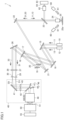
Fig. 1 is a schematic diagram of a Raman spectroscopy device of an embodiment. -
Fig. 2 is a partially enlarged schematic diagram of a photodetector of the Raman spectroscopy device of the embodiment. - In the following, an embodiment of the present disclosure will be described. Same components will be denoted by a same reference sign, and a repeated description will be omitted.
- With reference to
Figs. 1 and2 , a Raman spectroscopy device 1 of an embodiment will be described. Raman spectroscopy device 1 includes a firstexcitation light source 10, a secondexcitation light source 12, asample support portion 25a, a spectroscopicoptical system 40, aphotodetector 50, asignal processor 55,mirrors pass filters dichroic mirror 20,condenser lenses slits illumination light source 60, anobjective lens 24, asemitransparent mirror 23, animaging lens 62, and acamera 63. - First
excitation light source 10 outputs a firstexcitation light beam 11. Secondexcitation light source 12 outputs a secondexcitation light beam 13 that has a shorter wavelength than firstexcitation light beam 11. A first wavelength of firstexcitation light beam 11 may be different from a second wavelength of secondexcitation light beam 13 by 40 nm or more, or 100 nm or more, or 200 nm or more. In an example, the first wavelength of firstexcitation light beam 11 is 785 nm, and the second wavelength of secondexcitation light beam 13 is 532 nm. In another example, the first wavelength of firstexcitation light beam 11 is 1064 nm, and the second wavelength of secondexcitation light beam 13 is 532 nm. For example, firstexcitation light source 10 and secondexcitation light source 12 are laser light sources, and firstexcitation light beam 11 and secondexcitation light beam 13 are laser beams. For example, firstexcitation light source 10 and secondexcitation light source 12 are diode laser-pumped solid-state lasers, helium-neon lasers, titanium-sapphire lasers, or Nd:YAG lasers. - A
sample 25 is supported bysample support portion 25a such as a sample stage. One of firstexcitation light beam 11 and secondexcitation light beam 13 is irradiated onsample 25, depending onsample 25. The shorter the excitation wavelength, the higher the efficiency of Raman scattering. Accordingly, to increase intensity of Raman scattered light,sample 25 is irradiated not with firstexcitation light beam 11 but with secondexcitation light beam 13. In the case wheresample 25 emits strong fluorescence whensample 25 is irradiated with secondexcitation light beam 13,sample 25 is irradiated not with secondexcitation light beam 13 but with firstexcitation light beam 11. Accordingly, a Raman spectrum ofsample 25 may be obtained without being affected by the fluorescence. - First
excitation light beam 11 output from firstexcitation light source 10 is reflected bymirrors pass filter 17. Low-pass filter 17 reflects firstexcitation light beam 11, and transmits first Raman scatteredlight 31. Firstexcitation light beam 11 is reflected by low-pass filter 17, and entersdichroic mirror 20.Dichroic mirror 20 transmits firstexcitation light beam 11 and first Raman scatteredlight 31, and reflects secondexcitation light beam 13 and second Raman scatteredlight 33. Firstexcitation light beam 11 passes throughdichroic mirror 20. Firstexcitation light beam 11 is reflected bymirrors excitation light beam 11 passes throughsemitransparent mirror 23 andobjective lens 24, and is irradiated onsample 25. - Second
excitation light beam 13 output from secondexcitation light source 12 is reflected bymirrors pass filter 18. Low-pass filter 18 reflects secondexcitation light beam 13, and transmits second Raman scatteredlight 33. Secondexcitation light beam 13 is reflected by low-pass filter 18,mirror 19, anddichroic mirror 20. Secondexcitation light beam 13 is reflected bymirrors excitation light beam 13 passes throughsemitransparent mirror 23 andobjective lens 24, and is irradiated onsample 25. - When
sample 25 is irradiated with firstexcitation light beam 11, first Raman scatteredlight 31 is emitted fromsample 25. First Raman scatteredlight 31 has a longer wavelength than firstexcitation light beam 11. First Raman scatteredlight 31 passes throughobjective lens 24 andsemitransparent mirror 23, and is reflected bymirrors light 31 passes throughdichroic mirror 20 and low-pass filter 17, and is reflected bymirror 26. First Raman scatteredlight 31 is concentrated bycondenser lens 27, passes throughslit 29, and enters spectroscopicoptical system 40. - When
sample 25 is irradiated with secondexcitation light beam 13, second Raman scatteredlight 33 is emitted fromsample 25. Second Raman scatteredlight 33 has a longer wavelength than secondexcitation light beam 13. Second Raman scatteredlight 33 has a shorter wavelength than first Raman scatteredlight 31. That is, first Raman scatteredlight 31 is long-wavelength Raman scattered light, and second Raman scatteredlight 33 is short-wavelength Raman scattered light. Second Raman scatteredlight 33 passes throughobjective lens 24 andsemitransparent mirror 23, and is reflected bymirrors light 33 is reflected bydichroic mirror 20 andmirror 19. Second Raman scatteredlight 33 passes through low-pass filter 18, and is reflected bymirror 26. Second Raman scatteredlight 33 is concentrated bycondenser lens 28, passes throughslit 30, and enters spectroscopicoptical system 40. The position of an opening ofslit 30 is different from the position of an opening ofslit 29. - Spectroscopic
optical system 40 includescollimator lenses first spectrometer 44, a second spectrometer 46, and a condensingoptical element 49. Spectroscopicoptical system 40 may further include amirror 41. - First Raman scattered light 31 is reflected by
mirror 41, and enterscollimator lens 42.Collimator lens 42 collimates first Raman scatteredlight 31. First Raman scattered light 31 passes throughcollimator lens 42, and entersfirst spectrometer 44.First spectrometer 44 disperses first Raman scatteredlight 31. First Raman scattered light 31 dispersed byfirst spectrometer 44 passes through condensingoptical element 49, and entersphotodetector 50. Condensingoptical element 49 is a condenser lens, for example. Condensingoptical element 49 causes first Raman scattered light 31 dispersed byfirst spectrometer 44 to be concentrated on alight receiving surface 51 ofphotodetector 50 as a plurality of first beam spots 32 (seeFig. 2 ). - Second Raman scattered light 33 is reflected by
mirror 41, and enterscollimator lens 43.Collimator lens 43 collimates second Raman scatteredlight 33. Second Raman scattered light 33 passes throughcollimator lens 43, and enters second spectrometer 46. A secondincident light path 33i, inside spectroscopicoptical system 40, of second Raman scattered light 33 to second spectrometer 46 is different from a first incident light path 31i, inside spectroscopicoptical system 40, of first Raman scattered light 31 tofirst spectrometer 44. Second spectrometer 46 disperses second Raman scatteredlight 33. Second Raman scattered light 33 dispersed by second spectrometer 46 passes through condensingoptical element 49, and entersphotodetector 50. Condensingoptical element 49 causes second Raman scattered light 33 dispersed by second spectrometer 46 to be concentrated on light receivingsurface 51 ofphotodetector 50 as a plurality of second beam spots 34 (seeFig. 2 ). - Second spectrometer 46 is formed from a greater number of spectral optical elements than
first spectrometer 44. The spectral optical element is a grating or a prism, for example.First spectrometer 44 is formed from one first spectraloptical element 45. Second spectrometer 46 is formed from two second spectraloptical elements 47, 48. -
Photodetector 50 receives first Raman scattered light 31 and second Raman scattered light 33 output from spectroscopicoptical system 40. For example,photodetector 50 is a CCD detector. As shown inFig. 2 ,photodetector 50 includeslight receiving surface 51 that extends in a first direction (x-direction) and a second direction (y-direction) that intersects the first direction.Photodetector 50 includes a plurality ofphotodetection elements 52. For example, plurality ofphotodetection elements 52 are a plurality of CCD chips. Plurality ofphotodetection elements 52 are arranged two-dimensionally. More specifically, plurality ofphotodetection elements 52 are arranged on light receivingsurface 51, in the first direction (the x-direction) and the second direction (the y-direction). The second direction is a wavenumber resolution direction, onlight receiving surface 51, of first Raman scattered light 31 byfirst spectrometer 44, and is also a wavenumber resolution direction, onlight receiving surface 51, of second Raman scattered light 33 by second spectrometer 46. Plurality of first beam spots 32 are separated from one another in the first direction (the x-direction). Plurality of second beam spots 34 are separated from one another in the first direction (the x-direction). - When a light path of second Raman scattered light 33 is shifted, positions of plurality of second beam spots 34 on
light receiving surface 51 ofphotodetector 50 may become shifted from positions of plurality of first beam spots 32 (for example, see a plurality ofsecond beam spots 34b, 34c inFig. 2 ). However, because plurality ofphotodetection elements 52 are two-dimensionally arranged, even when the light path of second Raman scattered light 33 is shifted and the positions of plurality of second beam spots 34 are shifted,photodetector 50 may reliably receive second Raman scattered light 33 (plurality of second beam spots 34). In the same manner, even when a light path of first Raman scattered light 31 is shifted and positions of plurality of first beam spots 32 onlight receiving surface 51 ofphotodetector 50 are shifted,photodetector 50 may reliably receive first Raman scattered light 31 (plurality of first beam spots 32). - Referring to
Fig. 1 ,signal processor 55 is connected tophotodetector 50. A plurality of electrical signals output from plurality ofphotodetection elements 52 are processed. For example,signal processor 55 is a microcomputer including a processor, a random access memory (RAM), and a memory device such as a read only memory (ROM). As the processor, a central processing unit (CPU) may be adopted, for example. The RAM functions as a work memory that temporarily stores data that is processed by the processor. The memory device stores programs to be executed by the processor, for example.Signal processor 55 processes the plurality of electrical signals output from plurality ofphotodetection elements 52 through execution by the processor of a program stored in the memory device. Various processes bysignal processor 55 do not have to be performed by software, and may instead be performed by dedicated hardware (electronic circuit). - For example,
signal processor 55 performs binning processing on the plurality of electrical signals output from plurality ofphotodetection elements 52. The binning processing refers to collective processing of electrical signals output fromphotodetection elements 52, the processing being performed for each of a plurality ofphotodetection element groups 53a to 53k (seeFig. 2 ) among plurality ofphotodetection elements 52. For example, each of plurality ofphotodetection element groups 53a to 53k includes two rows ofphotodetection elements 52 among plurality ofphotodetection elements 52. For example,signal processor 55 may calculate a sum of electrical signals output fromphotodetection elements 52, for each of plurality ofphotodetection element groups 53a to 53k, or may calculate an average of electrical signals output fromphotodetection elements 52, for each of plurality ofphotodetection element groups 53a to 53k. - Even when first Raman scattered light 31 and second Raman scattered light 33 are weak, electrical signals of first Raman scattered light 31 and second Raman scattered light 33 may be reliably obtained by the binning processing. Furthermore, even when the light path of second Raman scattered light 33 is shifted and the positions of plurality of second beam spots 34 on
light receiving surface 51 ofphotodetector 50 are shifted (for example, see plurality ofsecond beam spots 34b, 34c inFig. 2 ), the binning processing allows accurate light intensity of each of plurality of second beam spots 34 to be obtained. An accurate Raman spectrum of second Raman scattered light 33 may be obtained by the binning processing. In the same manner, even when the light path of first Raman scattered light 31 is shifted and the positions of plurality of first beam spots 32 onlight receiving surface 51 ofphotodetector 50 are shifted, an accurate Raman spectrum of first Raman scattered light 31 may be obtained by the binning processing. - Raman spectroscopy device 1 may further include
illumination light source 60,objective lens 24,camera 63, andimaging lens 62, and may be a Raman spectroscopy microscope. -
Illumination light source 60 emitsillumination light 61 for illuminatingsample 25. For example,illumination light source 60 is a light-emitting diode (LED). For example,illumination light 61 is visible light.Illumination light 61 that is irradiated onsample 25 passes throughobjective lens 24, and is reflected bysemitransparent mirror 23. Illumination light 61 passes throughimaging lens 62, and enterscamera 63.Imaging lens 62 forms an image ofsample 25 on alight receiving surface 64 ofcamera 63.Camera 63 includes a CMOS sensor, for example. - Advantageous effects of Raman spectroscopy device 1 of the present embodiment will be described in comparison with Raman spectroscopy devices of first to third comparative examples.
- The Raman spectroscopy device of the first comparative example includes a first condensing optical element and a first photodetector for first Raman scattered light 31, and a second condensing optical element and a second photodetector for second Raman scattered
light 33. In contrast, with Raman spectroscopy device 1 of the present embodiment, condensingoptical element 49 andphotodetector 50 are used for both first Raman scattered light 31 and second Raman scatteredlight 33. The number of condensing optical elements and the number of photodetectors are smaller for Raman spectroscopy device 1 of the present embodiment than for the Raman spectroscopy device of the first comparative example. Accordingly, the cost of Raman spectroscopy device 1 of the present embodiment is lower than that of the Raman spectroscopy device of the first comparative example. - Because the second wavelength of second
excitation light beam 13 is shorter than the first wavelength of firstexcitation light beam 11, a wavelength range of second Raman scattered light 33 corresponding to a certain measurable wavenumber range is smaller than a wavelength range of first Raman scattered light 31 corresponding to the measurable wavenumber range in question. To increase a measurable wavenumber range of the Raman spectrum of second Raman scattered light 33 to about the same as a measurable wavenumber range of the Raman spectrum of first Raman scattered light 31, for example, angular dispersion of second spectrometer 46 has to be made greater than angular dispersion offirst spectrometer 44. - With the Raman spectroscopy device of the second comparative example,
first spectrometer 44 and second spectrometer 46 are formed from the same number of spectral optical elements, and the spectral optical element forming second spectrometer 46 has greater angular dispersion than the spectral optical element formingfirst spectrometer 44. However, the cost of the spectral optical element is drastically increased as wavelength resolution of the spectral optical element is increased. Accordingly, with the Raman spectroscopy device of the second comparative example, when the measurable wavenumber range of the Raman spectrum of second Raman scattered light 33 is increased to about the same as the measurable wavenumber range of the Raman spectrum of first Raman scattered light 31, for example, the cost of the Raman spectroscopy device of the second comparative example is increased. - In contrast, with Raman spectroscopy device 1 of the present embodiment, second spectrometer 46 is formed from a greater number of spectral optical elements than
first spectrometer 44. Accordingly, the angular dispersion of second spectrometer 46 may be made greater than the angular dispersion offirst spectrometer 44 while using an inexpensive spectral optical element as each of a plurality of spectral optical elements forming second spectrometer 46. Accordingly, the cost of Raman spectroscopy device 1 of the present embodiment is reduced than the cost of the Raman spectroscopy device of the second comparative example even when the measurable wavenumber range of the Raman spectrum of second Raman scattered light 33 is increased to about the same as the measurable wavenumber range of the Raman spectrum of first Raman scattered light 31, for example. - With the Raman spectroscopy device of the third comparative example, second
incident light path 33i, inside spectroscopicoptical system 40, of second Raman scattered light 33 to second spectrometer 46 is the same as first incident light path 31i, inside spectroscopicoptical system 40, of first Raman scattered light 31 tofirst spectrometer 44. Accordingly, the Raman spectroscopy device of the third comparative example requires a movement mechanism for switching betweenfirst spectrometer 44 and second spectrometer 46. - In contrast, with Raman spectroscopy device 1 of the present embodiment, second
incident light path 33i, inside spectroscopicoptical system 40, of second Raman scattered light 33 to second spectrometer 46 is different from first incident light path 31i, inside spectroscopicoptical system 40, of first Raman scattered light 31 tofirst spectrometer 44. Accordingly, Raman spectroscopy device 1 does not need a movement mechanism for movingfirst spectrometer 44 and second spectrometer 46. The cost of Raman spectroscopy device 1 of the present embodiment is lower than the cost of the Raman spectroscopy device of the third comparative example. The Raman spectrum of first Raman scattered light 31 and the Raman spectrum of second Raman scattered light 33 may be more accurately and stably obtained by Raman spectroscopy device 1 of the present embodiment than by the Raman spectroscopy device of the third comparative example. - With Raman spectroscopy device 1 of a modification of the present embodiment, the number of excitation light sources may be three or more.
- The exemplary embodiment described above should be understood by those skilled in the art to be a specific example of the modes described below.
- (First Aspect) A Raman spectroscopy device according to a mode includes a spectroscopic optical system and a photodetector. The spectroscopic optical system includes a first spectrometer and a second spectrometer. The first spectrometer disperses first Raman scattered light that is emitted from a sample when the sample is irradiated with a first excitation light beam. The second spectrometer disperses second Raman scattered light that is emitted from the sample when the sample is irradiated with a second excitation light beam having a shorter wavelength than the first excitation light beam, the second Raman scattered light having a shorter wavelength than the first Raman scattered light. The photodetector receives the first Raman scattered light and the second Raman scattered light output from the spectroscopic optical system. A second incident light path, inside the spectroscopic optical system, of the second Raman scattered light to the second spectrometer is different from a first incident light path, inside the spectroscopic optical system, of the first Raman scattered light to the first spectrometer. The second spectrometer is formed from a greater number of spectral optical elements than the first spectrometer.
- The photodetector is used for both the first Raman scattered light and the second Raman scattered light. Accordingly, the cost of the Raman spectroscopy device is reduced. Furthermore, the second spectrometer is formed from a greater number of spectral optical elements than the first spectrometer, and thus, the angular dispersion of the second spectrometer may be increased while using low-cost spectral optical elements as the spectral optical elements that form the second spectrometer. Accordingly, the measurable wavenumber range of the Raman spectrum of the second Raman scattered light may be increased, and also, the cost of the Raman spectroscopy device is reduced. Moreover, the second incident light path, inside the spectroscopic optical system, of the second Raman scattered light to the second spectrometer is different from the first incident light path, inside the spectroscopic optical system, of the first Raman scattered light to the first spectrometer. Accordingly, the Raman spectroscopy device does not need a movement mechanism for moving the first spectrometer and the second spectrometer. The cost of the Raman spectroscopy device is reduced.
- (Second Aspect) With the Raman spectroscopy device according to the first aspect, the first spectrometer is formed from one spectral optical element. The second spectrometer is formed from two spectral optical elements.
- Accordingly, the number of spectral optical elements for forming the first spectrometer and the second spectrometer may be minimized. The cost of the Raman spectroscopy device is reduced.
- (Third Aspect) With the Raman spectroscopy device according to the first or second aspect, the spectroscopic optical system includes a condensing optical element. The condensing optical element causes the first Raman scattered light output from the first spectrometer and the second Raman scattered light output from the second spectrometer to be concentrated on the photodetector.
- The condensing optical element is used for both the first Raman scattered light and the second Raman scattered light. Accordingly, the cost of the Raman spectroscopy device is reduced.
- (Fourth Aspect) With the Raman spectroscopy device according to any one of the first to third aspects, the photodetector includes a plurality of photodetection elements that are two-dimensionally arranged.
- Accordingly, even when a light path of the first Raman scattered light or a light path of the second Raman scattered light is shifted, the photodetector is able to reliably receive the first Raman scattered light and the second Raman scattered light. The Raman spectroscopy device is able to reliably obtain the Raman spectrum. Freedom of design of the optical system of the Raman spectroscopy device is increased.
- (Fifth Aspect) The Raman spectroscopy device according to the fourth aspect further includes a signal processor that is connected to the photodetector. The signal processor performs binning processing on a plurality of electrical signals that are output from the plurality of photodetection elements.
- Accordingly, even when the first Raman scattered light and the second Raman scattered light are weak, electrical signals of the first Raman scattered light and the second Raman scattered light may be reliably obtained. Even when the light path of the first Raman scattered light or the light path of the second Raman scattered light is shifted, the Raman spectrum of the first Raman scattered light and the Raman spectrum of the second Raman scattered light may be obtained more accurately.
- The embodiment and the modification disclosed herein are illustrative in every aspect, and should be understood to be non-restrictive. The scope of the present disclosure is indicated not by the description given above but by the scope of the claims, and is intended to include all the changes within the scope and meaning equivalent to those of the scope of the claims.
- 1 Raman spectroscopy device; 10 first excitation light source; 11 first excitation light beam; 12 second excitation light source; 13 second excitation light beam; 15, 16, 19, 21, 22, 26, 41 mirror; 17, 18 low-pass filter; 20 dichroic mirror; 23 semitransparent mirror; 24 objective lens; 25 sample; 25a sample support portion; 27, 28 condenser lens; 29, 30 slit; 31 first Raman scattered light; 31i first incident light path; 32 first beam spot; 33 second Raman scattered light; 33i second incident light path; 34, 34b, 34c second beam spot; 40 spectroscopic optical system; 42, 43 collimator lens; 44 first spectrometer; 45 first spectral optical element; 46 second spectrometer; 47, 48 second spectral optical element; 49 condensing optical element; 50 photodetector; 51 light receiving surface; 52 photodetection element; 53a to 53k photodetection element group; 55 signal processor; 60 illumination light source; 61 illumination light; 62 imaging lens; 63 camera; 64 light receiving surface
Claims (5)
- A Raman spectroscopy device comprising:a spectroscopic optical system; anda photodetector, whereinthe spectroscopic optical system includes a first spectrometer for dispersing first Raman scattered light that is emitted from a sample when the sample is irradiated with a first excitation light beam, and a second spectrometer for dispersing second Raman scattered light that is emitted from the sample when the sample is irradiated with a second excitation light beam having a shorter wavelength than the first excitation light beam, the second Raman scattered light having a shorter wavelength than the first Raman scattered light,the photodetector receives the first Raman scattered light and the second Raman scattered light output from the spectroscopic optical system,a second incident light path, inside the spectroscopic optical system, of the second Raman scattered light to the second spectrometer is different from a first incident light path, inside the spectroscopic optical system, of the first Raman scattered light to the first spectrometer, andthe second spectrometer is formed from a greater number of spectral optical elements than the first spectrometer.
- The Raman spectroscopy device according to claim 1, whereinthe first spectrometer is formed from one spectral optical element, andthe second spectrometer is formed from two spectral optical elements.
- The Raman spectroscopy device according to claim 1 or 2, whereinthe spectroscopic optical system includes a condensing optical element, andthe condensing optical element causes the first Raman scattered light output from the first spectrometer and the second Raman scattered light output from the second spectrometer to be concentrated on the photodetector.
- The Raman spectroscopy device according to any one of claims 1 to 3, wherein the photodetector includes a plurality of photodetection elements that are two-dimensionally arranged.
- The Raman spectroscopy device according to claim 4, further comprising a signal processor that is connected to the photodetector, wherein
the signal processor performs binning processing on a plurality of electrical signals that are output from the plurality of photodetection elements.
Applications Claiming Priority (2)
| Application Number | Priority Date | Filing Date | Title |
|---|---|---|---|
| JP2021141144 | 2021-08-31 | ||
| PCT/JP2022/010759 WO2023032290A1 (en) | 2021-08-31 | 2022-03-11 | Raman spectroscopy device |
Publications (2)
| Publication Number | Publication Date |
|---|---|
| EP4397961A1 true EP4397961A1 (en) | 2024-07-10 |
| EP4397961A4 EP4397961A4 (en) | 2025-07-23 |
Family
ID=85412445
Family Applications (1)
| Application Number | Title | Priority Date | Filing Date |
|---|---|---|---|
| EP22863880.5A Pending EP4397961A4 (en) | 2021-08-31 | 2022-03-11 | RAMAN SPECTROSCOPY DEVICE |
Country Status (5)
| Country | Link |
|---|---|
| US (1) | US20260118177A1 (en) |
| EP (1) | EP4397961A4 (en) |
| JP (1) | JP7694673B2 (en) |
| CN (1) | CN117881957A (en) |
| WO (1) | WO2023032290A1 (en) |
Family Cites Families (6)
| Publication number | Priority date | Publication date | Assignee | Title |
|---|---|---|---|---|
| JPS5010512B1 (en) * | 1968-04-11 | 1975-04-22 | ||
| WO2014060118A1 (en) * | 2012-10-16 | 2014-04-24 | Avantes Holding B.V. | Dual beam device for simultaneous measurement of spectrum and polarization of light |
| US8873041B1 (en) | 2013-01-29 | 2014-10-28 | Bayspec, Inc. | Raman spectroscopy using multiple excitation wavelengths |
| JP6754492B2 (en) * | 2018-01-18 | 2020-09-09 | 小出 珠貴 | Biological tissue analyzer and biological tissue analysis method |
| JP7456639B2 (en) * | 2019-03-28 | 2024-03-27 | 国立大学法人 東京大学 | spectrometer |
| CN113631897B (en) * | 2019-04-29 | 2024-07-16 | Atonarp株式会社 | Hybrid optical system |
-
2022
- 2022-03-11 CN CN202280059040.6A patent/CN117881957A/en active Pending
- 2022-03-11 JP JP2023545042A patent/JP7694673B2/en active Active
- 2022-03-11 US US18/687,813 patent/US20260118177A1/en active Pending
- 2022-03-11 WO PCT/JP2022/010759 patent/WO2023032290A1/en not_active Ceased
- 2022-03-11 EP EP22863880.5A patent/EP4397961A4/en active Pending
Also Published As
| Publication number | Publication date |
|---|---|
| JP7694673B2 (en) | 2025-06-18 |
| JPWO2023032290A1 (en) | 2023-03-09 |
| US20260118177A1 (en) | 2026-04-30 |
| EP4397961A4 (en) | 2025-07-23 |
| CN117881957A (en) | 2024-04-12 |
| WO2023032290A1 (en) | 2023-03-09 |
Similar Documents
| Publication | Publication Date | Title |
|---|---|---|
| US5422712A (en) | Apparatus for measuring fluorescent spectra of particles in a flow | |
| US7561265B2 (en) | Optical microscope and spectrum measuring method | |
| US8873046B2 (en) | Spectroscopic detection device and confocal microscope | |
| JP6055087B2 (en) | Light emitting device for emitting a light beam of controlled spectrum | |
| JP4817356B2 (en) | Optical microscope | |
| JP2011237384A (en) | Optical system for analysis and analyzer using the same | |
| JP2001235684A (en) | Confocal scanning microscope | |
| JP4645176B2 (en) | Spectroscopic microscope | |
| CN101467182B (en) | Device and method for optical checking of documents of value | |
| ES2911722T3 (en) | Spectrophotometer | |
| CN116710828B (en) | Method and optical microscope having an array of multiple photon counting detector elements | |
| JP2012003198A (en) | Microscope | |
| EP4397961A1 (en) | Raman spectroscopy device | |
| JPWO2023013325A5 (en) | ||
| US11340114B2 (en) | Spectrum measurement system | |
| JP2009230021A (en) | Optical microscope and spectrum measuring method | |
| JP2011058953A (en) | Detector, optical apparatus with the same | |
| JP2004354344A (en) | Light source device and biomolecule analysis apparatus using the light source device | |
| JP2017151373A (en) | Infrared microscope and infrared microscope system | |
| JP2004354346A (en) | Measuring device | |
| US20250012727A1 (en) | Optical axis adjustment method for laser module and optical axis adjustment jig | |
| EP4397963A1 (en) | Optical axis adjustment method for laser module and optical axis adjustment jig | |
| CN220305493U (en) | Photoelectric detector test system and laser radar | |
| JP2013195264A (en) | Spectroscope and microspectroscopic system | |
| WO2025115175A1 (en) | Microspectroscopy device |
Legal Events
| Date | Code | Title | Description |
|---|---|---|---|
| STAA | Information on the status of an ep patent application or granted ep patent |
Free format text: STATUS: THE INTERNATIONAL PUBLICATION HAS BEEN MADE |
|
| PUAI | Public reference made under article 153(3) epc to a published international application that has entered the european phase |
Free format text: ORIGINAL CODE: 0009012 |
|
| STAA | Information on the status of an ep patent application or granted ep patent |
Free format text: STATUS: REQUEST FOR EXAMINATION WAS MADE |
|
| 17P | Request for examination filed |
Effective date: 20240328 |
|
| AK | Designated contracting states |
Kind code of ref document: A1 Designated state(s): AL AT BE BG CH CY CZ DE DK EE ES FI FR GB GR HR HU IE IS IT LI LT LU LV MC MK MT NL NO PL PT RO RS SE SI SK SM TR |
|
| DAV | Request for validation of the european patent (deleted) | ||
| DAX | Request for extension of the european patent (deleted) | ||
| A4 | Supplementary search report drawn up and despatched |
Effective date: 20250624 |
|
| RIC1 | Information provided on ipc code assigned before grant |
Ipc: G01N 21/65 20060101AFI20250617BHEP Ipc: G01J 3/02 20060101ALI20250617BHEP Ipc: G01J 3/10 20060101ALI20250617BHEP Ipc: G01J 3/44 20060101ALI20250617BHEP Ipc: G01J 3/28 20060101ALI20250617BHEP |