EP4395515A1 - Organic light emitting diode and organic light emitting device including the same - Google Patents
Organic light emitting diode and organic light emitting device including the same Download PDFInfo
- Publication number
- EP4395515A1 EP4395515A1 EP23194259.0A EP23194259A EP4395515A1 EP 4395515 A1 EP4395515 A1 EP 4395515A1 EP 23194259 A EP23194259 A EP 23194259A EP 4395515 A1 EP4395515 A1 EP 4395515A1
- Authority
- EP
- European Patent Office
- Prior art keywords
- dopant
- formula
- unsubstituted
- substituted
- emitting layer
- Prior art date
- Legal status (The legal status is an assumption and is not a legal conclusion. Google has not performed a legal analysis and makes no representation as to the accuracy of the status listed.)
- Granted
Links
Images




Classifications
-
- H—ELECTRICITY
- H10—SEMICONDUCTOR DEVICES; ELECTRIC SOLID-STATE DEVICES NOT OTHERWISE PROVIDED FOR
- H10K—ORGANIC ELECTRIC SOLID-STATE DEVICES
- H10K85/00—Organic materials used in the body or electrodes of devices covered by this subclass
- H10K85/60—Organic compounds having low molecular weight
- H10K85/631—Amine compounds having at least two aryl rest on at least one amine-nitrogen atom, e.g. triphenylamine
- H10K85/633—Amine compounds having at least two aryl rest on at least one amine-nitrogen atom, e.g. triphenylamine comprising polycyclic condensed aromatic hydrocarbons as substituents on the nitrogen atom
-
- H—ELECTRICITY
- H10—SEMICONDUCTOR DEVICES; ELECTRIC SOLID-STATE DEVICES NOT OTHERWISE PROVIDED FOR
- H10K—ORGANIC ELECTRIC SOLID-STATE DEVICES
- H10K50/00—Organic light-emitting devices
- H10K50/10—OLEDs or polymer light-emitting diodes [PLED]
- H10K50/11—OLEDs or polymer light-emitting diodes [PLED] characterised by the electroluminescent [EL] layers
- H10K50/12—OLEDs or polymer light-emitting diodes [PLED] characterised by the electroluminescent [EL] layers comprising dopants
-
- C—CHEMISTRY; METALLURGY
- C09—DYES; PAINTS; POLISHES; NATURAL RESINS; ADHESIVES; COMPOSITIONS NOT OTHERWISE PROVIDED FOR; APPLICATIONS OF MATERIALS NOT OTHERWISE PROVIDED FOR
- C09K—MATERIALS FOR MISCELLANEOUS APPLICATIONS, NOT PROVIDED FOR ELSEWHERE
- C09K11/00—Luminescent materials, e.g. electroluminescent or chemiluminescent
- C09K11/06—Luminescent materials, e.g. electroluminescent or chemiluminescent containing organic luminescent materials
-
- H—ELECTRICITY
- H10—SEMICONDUCTOR DEVICES; ELECTRIC SOLID-STATE DEVICES NOT OTHERWISE PROVIDED FOR
- H10K—ORGANIC ELECTRIC SOLID-STATE DEVICES
- H10K50/00—Organic light-emitting devices
- H10K50/10—OLEDs or polymer light-emitting diodes [PLED]
- H10K50/11—OLEDs or polymer light-emitting diodes [PLED] characterised by the electroluminescent [EL] layers
- H10K50/125—OLEDs or polymer light-emitting diodes [PLED] characterised by the electroluminescent [EL] layers specially adapted for multicolour light emission, e.g. for emitting white light
- H10K50/13—OLEDs or polymer light-emitting diodes [PLED] characterised by the electroluminescent [EL] layers specially adapted for multicolour light emission, e.g. for emitting white light comprising stacked EL layers within one EL unit
-
- H—ELECTRICITY
- H10—SEMICONDUCTOR DEVICES; ELECTRIC SOLID-STATE DEVICES NOT OTHERWISE PROVIDED FOR
- H10K—ORGANIC ELECTRIC SOLID-STATE DEVICES
- H10K50/00—Organic light-emitting devices
- H10K50/10—OLEDs or polymer light-emitting diodes [PLED]
- H10K50/19—Tandem OLEDs
-
- H—ELECTRICITY
- H10—SEMICONDUCTOR DEVICES; ELECTRIC SOLID-STATE DEVICES NOT OTHERWISE PROVIDED FOR
- H10K—ORGANIC ELECTRIC SOLID-STATE DEVICES
- H10K59/00—Integrated devices, or assemblies of multiple devices, comprising at least one organic light-emitting element covered by group H10K50/00
- H10K59/10—OLED displays
- H10K59/12—Active-matrix OLED [AMOLED] displays
-
- H—ELECTRICITY
- H10—SEMICONDUCTOR DEVICES; ELECTRIC SOLID-STATE DEVICES NOT OTHERWISE PROVIDED FOR
- H10K—ORGANIC ELECTRIC SOLID-STATE DEVICES
- H10K59/00—Integrated devices, or assemblies of multiple devices, comprising at least one organic light-emitting element covered by group H10K50/00
- H10K59/80—Constructional details
- H10K59/87—Passivation; Containers; Encapsulations
- H10K59/873—Encapsulations
-
- H—ELECTRICITY
- H10—SEMICONDUCTOR DEVICES; ELECTRIC SOLID-STATE DEVICES NOT OTHERWISE PROVIDED FOR
- H10K—ORGANIC ELECTRIC SOLID-STATE DEVICES
- H10K85/00—Organic materials used in the body or electrodes of devices covered by this subclass
- H10K85/30—Coordination compounds
- H10K85/321—Metal complexes comprising a group IIIA element, e.g. Tris (8-hydroxyquinoline) gallium [Gaq3]
- H10K85/322—Metal complexes comprising a group IIIA element, e.g. Tris (8-hydroxyquinoline) gallium [Gaq3] comprising boron
-
- H—ELECTRICITY
- H10—SEMICONDUCTOR DEVICES; ELECTRIC SOLID-STATE DEVICES NOT OTHERWISE PROVIDED FOR
- H10K—ORGANIC ELECTRIC SOLID-STATE DEVICES
- H10K85/00—Organic materials used in the body or electrodes of devices covered by this subclass
- H10K85/60—Organic compounds having low molecular weight
- H10K85/615—Polycyclic condensed aromatic hydrocarbons, e.g. anthracene
-
- H—ELECTRICITY
- H10—SEMICONDUCTOR DEVICES; ELECTRIC SOLID-STATE DEVICES NOT OTHERWISE PROVIDED FOR
- H10K—ORGANIC ELECTRIC SOLID-STATE DEVICES
- H10K85/00—Organic materials used in the body or electrodes of devices covered by this subclass
- H10K85/60—Organic compounds having low molecular weight
- H10K85/615—Polycyclic condensed aromatic hydrocarbons, e.g. anthracene
- H10K85/622—Polycyclic condensed aromatic hydrocarbons, e.g. anthracene containing four rings, e.g. pyrene
-
- H—ELECTRICITY
- H10—SEMICONDUCTOR DEVICES; ELECTRIC SOLID-STATE DEVICES NOT OTHERWISE PROVIDED FOR
- H10K—ORGANIC ELECTRIC SOLID-STATE DEVICES
- H10K85/00—Organic materials used in the body or electrodes of devices covered by this subclass
- H10K85/60—Organic compounds having low molecular weight
- H10K85/615—Polycyclic condensed aromatic hydrocarbons, e.g. anthracene
- H10K85/626—Polycyclic condensed aromatic hydrocarbons, e.g. anthracene containing more than one polycyclic condensed aromatic rings, e.g. bis-anthracene
-
- H—ELECTRICITY
- H10—SEMICONDUCTOR DEVICES; ELECTRIC SOLID-STATE DEVICES NOT OTHERWISE PROVIDED FOR
- H10K—ORGANIC ELECTRIC SOLID-STATE DEVICES
- H10K85/00—Organic materials used in the body or electrodes of devices covered by this subclass
- H10K85/60—Organic compounds having low molecular weight
- H10K85/649—Aromatic compounds comprising a hetero atom
- H10K85/657—Polycyclic condensed heteroaromatic hydrocarbons
- H10K85/6574—Polycyclic condensed heteroaromatic hydrocarbons comprising only oxygen in the heteroaromatic polycondensed ring system, e.g. cumarine dyes
-
- H—ELECTRICITY
- H10—SEMICONDUCTOR DEVICES; ELECTRIC SOLID-STATE DEVICES NOT OTHERWISE PROVIDED FOR
- H10K—ORGANIC ELECTRIC SOLID-STATE DEVICES
- H10K85/00—Organic materials used in the body or electrodes of devices covered by this subclass
- H10K85/60—Organic compounds having low molecular weight
- H10K85/658—Organoboranes
-
- C—CHEMISTRY; METALLURGY
- C09—DYES; PAINTS; POLISHES; NATURAL RESINS; ADHESIVES; COMPOSITIONS NOT OTHERWISE PROVIDED FOR; APPLICATIONS OF MATERIALS NOT OTHERWISE PROVIDED FOR
- C09K—MATERIALS FOR MISCELLANEOUS APPLICATIONS, NOT PROVIDED FOR ELSEWHERE
- C09K2211/00—Chemical nature of organic luminescent or tenebrescent compounds
- C09K2211/10—Non-macromolecular compounds
- C09K2211/1003—Carbocyclic compounds
- C09K2211/1011—Condensed systems
-
- C—CHEMISTRY; METALLURGY
- C09—DYES; PAINTS; POLISHES; NATURAL RESINS; ADHESIVES; COMPOSITIONS NOT OTHERWISE PROVIDED FOR; APPLICATIONS OF MATERIALS NOT OTHERWISE PROVIDED FOR
- C09K—MATERIALS FOR MISCELLANEOUS APPLICATIONS, NOT PROVIDED FOR ELSEWHERE
- C09K2211/00—Chemical nature of organic luminescent or tenebrescent compounds
- C09K2211/10—Non-macromolecular compounds
- C09K2211/1018—Heterocyclic compounds
-
- H—ELECTRICITY
- H10—SEMICONDUCTOR DEVICES; ELECTRIC SOLID-STATE DEVICES NOT OTHERWISE PROVIDED FOR
- H10K—ORGANIC ELECTRIC SOLID-STATE DEVICES
- H10K2101/00—Properties of the organic materials covered by group H10K85/00
- H10K2101/90—Multiple hosts in the emissive layer
-
- H—ELECTRICITY
- H10—SEMICONDUCTOR DEVICES; ELECTRIC SOLID-STATE DEVICES NOT OTHERWISE PROVIDED FOR
- H10K—ORGANIC ELECTRIC SOLID-STATE DEVICES
- H10K50/00—Organic light-emitting devices
- H10K50/10—OLEDs or polymer light-emitting diodes [PLED]
- H10K50/11—OLEDs or polymer light-emitting diodes [PLED] characterised by the electroluminescent [EL] layers
-
- H—ELECTRICITY
- H10—SEMICONDUCTOR DEVICES; ELECTRIC SOLID-STATE DEVICES NOT OTHERWISE PROVIDED FOR
- H10K—ORGANIC ELECTRIC SOLID-STATE DEVICES
- H10K85/00—Organic materials used in the body or electrodes of devices covered by this subclass
- H10K85/60—Organic compounds having low molecular weight
- H10K85/649—Aromatic compounds comprising a hetero atom
- H10K85/657—Polycyclic condensed heteroaromatic hydrocarbons
Definitions
- the OLED includes a fist electrode as an anode over a substrate, a second electrode, which is spaced apart from and faces the first electrode, and an organic emitting layer therebetween.
- a gate line GL and a data line DL, which cross each other to define a pixel region (pixel) P, and a power line PL are formed in an organic light emitting display device.
- a switching thin film transistor (TFT) Ts, a driving TFT Td, a storage capacitor Cst and an OLED D are formed in the pixel region P.
- the pixel region P may include a red pixel region, a green pixel region and a blue pixel region.
- the switching thin film transistor Ts When the switching thin film transistor Ts is turned on by the gate signal applied through the gate line GL, the data signal applied through the data line DL is applied into a gate electrode of the driving thin film transistor Td and one electrode of the storage capacitor Cst through the switching thin film transistor Ts.
- the driving thin film transistor Td is turned on by the data signal applied into the gate electrode so that a current proportional to the data signal is supplied from the power line PL to the OLED D through the driving thin film transistor Td.
- the OLED D emits light having a luminance proportional to the current flowing through the driving thin film transistor Td.
- the storage capacitor Cst is charge with a voltage proportional to the data signal so that the voltage of the gate electrode in the driving thin film transistor Td is kept constant during one frame. Therefore, the organic light emitting display device can display a desired image.
- FIG. 2 is a schematic cross-sectional view illustrating an organic light emitting display device according to a first embodiment of the present invention.
- the organic light emitting display device 100 includes a substrate 110, a TFT Tr and an OLED D disposed on a planarization layer and connected to the TFT Tr.
- the substrate 110 may be a glass substrate or a flexible substrate.
- the flexible substrate may be a polyimide (PI) substrate, a polyethersulfone (PES) substrate, a polyethylenenaphthalate (PEN) substrate, a polyethylene terephthalate (PET) substrate or a polycarbonate (PC) substrate.
- PI polyimide
- PES polyethersulfone
- PEN polyethylenenaphthalate
- PET polyethylene terephthalate
- PC polycarbonate
- a buffer layer 120 is formed on the substrate, and the TFT Tr is formed on the buffer layer 120.
- the buffer layer 120 may be omitted.
- a semiconductor layer 122 is formed on the buffer layer 120.
- the semiconductor layer 122 may include an oxide semiconductor material or polycrystalline silicon.
- a light-shielding pattern (not shown) may be formed under the semiconductor layer 122. The light to the semiconductor layer 122 is shielded or blocked by the light-shielding pattern such that thermal degradation of the semiconductor layer 122 can be prevented.
- impurities may be doped into both sides of the semiconductor layer 122.
- a gate insulating layer 124 is formed on the semiconductor layer 122.
- the gate insulating layer 124 may be formed of an inorganic insulating material such as silicon oxide (SiOx) or silicon nitride (SiNx).
- a gate electrode 130 which is formed of a conductive material, e.g., metal, is formed on the gate insulating layer 124 to correspond to a center of the semiconductor layer 122.
- the gate insulating layer 124 is formed on an entire surface of the substrate 110.
- the gate insulating layer 124 may be patterned to have the same shape as the gate electrode 130.
- An interlayer insulating layer 132 which is formed of an insulating material, is formed on the gate electrode 130.
- the interlayer insulating layer 132 may be formed of an inorganic insulating material, e.g., silicon oxide or silicon nitride, or an organic insulating material, e.g., benzocyclobutene or photo-acryl.
- the interlayer insulating layer 132 includes first and second contact holes 134 and 136 exposing both sides of the semiconductor layer 122.
- the first and second contact holes 134 and 136 are positioned at both sides of the gate electrode 130 to be spaced apart from the gate electrode 130.
- the first and second contact holes 134 and 136 are formed through the gate insulating layer 124 and the interlayer insulating layer 132.
- the gate insulating layer 124 is patterned to have the same shape as the gate electrode 130, the first and second contact holes 134 and 136 is formed only through the interlayer insulating layer 132.
- a source electrode 140 and a drain electrode 142 which are formed of a conductive material, e.g., metal, are formed on the interlayer insulating layer 132.
- the source electrode 140 and the drain electrode 142 are spaced apart from each other with respect to the gate electrode 130 and respectively contact both sides of the semiconductor layer 122 through the first and second contact holes 134 and 136.
- the gate line and the data line cross each other to define the pixel region, and the switching TFT is formed to be connected to the gate and data lines.
- the switching TFT is connected to the TFT Tr as the driving element.
- the power line which may be formed to be parallel to and spaced apart from one of the gate and data lines, and the storage capacitor for maintaining the voltage of the gate electrode of the TFT Tr in one frame may be further formed.
- the first electrode 160 is separately formed in each pixel region.
- the first electrode 160 may be an anode and may be formed of a conductive material having a relatively high work function.
- the first electrode 160 may be formed of a conductive material having a relatively high work function, e.g., a transparent conductive oxide (TCO).
- TCO transparent conductive oxide
- the first electrode 160 may include at least one of indium-tin-oxide (ITO), indium-zinc-oxide (IZO), indium-tin-zinc oxide (ITZO), tin oxide (SnO), zinc oxide (ZnO), indium-copper-oxide (ICO) and aluminum-zinc-oxide (Al:ZnO, AZO).
- the first blue emitting layer includes a first host being a pyrene derivative (or compound) and a first dopant being one of a first compound represented by Formula 5 and a second compound represented by Formula 6, and the second blue emitting layer includes a second host being an anthracene derivative and a second dopant being one of a third compound represented by Formula 5 and a fourth compound represented by Formula 6.
- the OLED D and the organic light emitting display device 100 have an advantage in at least one of the driving voltage, the color purity, the emitting efficiency, and the lifespan.
- the organic light emitting display device 100 may include a color filter layer corresponding to the red, green and blue pixel regions.
- the color filter layer may include red, green and blue color filters respectively corresponding to the red, green and blue pixel regions.
- the organic light emitting display device 100 with the color filter layer may have improved color purity.
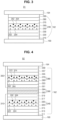
- FIG. 3 is a schematic cross-sectional view illustrating an OLED according to a second embodiment of the present invention.
- a weight % of the first host 252 in the first blue emitting layer 250 and a weight % of the second host 262 in the second blue emitting layer 260 may be same or different, and a weight % of the first dopant 254 in the first blue emitting layer 250 and a weight % of the second dopant 264 in the second blue emitting layer 260 may be same or different.
- a C3 to C30 heteroarylene group can be selected from the group consisting of pyrrolylene, pyridinylv, pyrimidinylene, pyrazinylene, pyridazinylene, triazinylene, tetrazinylene, imidazolylene, pyrazolylene, indolylene, isoindolylene, indazolylene, indolizinylene, pyrrolizinylene, carbazolylene, benzocarbazolylene, dibenzocarbazolylene, indolocarbazolylene, indenocarbazolylene, benzofurocarbazolylene, benzothienocarbazolylene, quinolinylene, isoquinolinylene, phthalazinylene, quinoxalinylene, cinnolinylene, quinazolinylene, quinolizinyl, quinolinylene, purinylene, phthalazinylene,
- each of Ar 1 and Ar 2 may be independently selected from the group consisting of hydrogen, a C6 to C30 aryl group, e.g., phenyl, naphthyl, fluorenyl, phenanthrenyl or pyrenyl, unsubstituted or substituted with at least one of a C1 to C10 alkyl group and a C6 to C30 aryl group, and a C3 to C30 heteroaryl group, e.g., dibenzothiophenyl, benzo[b]naphto[1,2-d]furanyl, or benzo[b]naphto[2,3-d]furanyl, unsubstituted or substituted with at least one of a C1 to C10 alkyl group and a C6 to C30 aryl group.
- a C6 to C30 aryl group e.g., phenyl, naphthyl, fluorenyl, phenanthrenyl or
- each of L 1 and L 2 may be independently a substituted or unsubstituted C6 to C30 arylene group, e.g., phenylene.
- the first host 252 included in the first blue EML 250 may include at least one of compounds in Formula 2as referred to herein above.
- each of b1 and b2 is independently 0 or 1
- b3 is an integer of 0 to 8
- one of b1 and b2 may be 0, and the other one of b1 and b2 may be 1.
- Each of L 11 and L 12 may be independently a substituted or unsubstituted C6 to C30 arylene group, e.g., phenylene.
- the second host 262 included in the second blue EML 260 may include at least one of compounds in Formula 4 as referred to herein above.
- the first dopant 254 is one of a first compound represented by Formula 5 and a second compound represented by Formula 6, and the second dopant 264 is one of a third compound represented by Formula 5 and a fourth compound represented by Formula 6.
- i) both of the first dopant 254 and the second dopant 264 are represented by Formula 5, and athe first dopant 254 and the second dopant 264 are same or different
- ii) the first dopant 254 is represented by Formula 5 and the second dopant 264 is represented by Formula 6
- iii) the first dopant 254 is represented by Formula 6
- the second dopant 264 is represented by Formula 5, or iv) both of the first dopant 254 and the second dopant 264 are represented by Formula 6, and the first dopant 254 and the second dopant 264 are same or different.
- each of e1, e2 and e3 is independently 0 or 1.
- each of e1 and e2 may be 0, and e3 may be 0 or 1.
- each of f1 and f2 is independently an integer of 0 to 4
- f3 is an integer of 0 to 3
- f4 is 0 or 1
- each of R 31 , R 32 and R 33 may be independently selected from the group consisting of a substituted or unsubstituted C1 to C30 alkyl group, e.g., methyl or tert-butyl, a C6 to C30 arylamino group, e.g., diphenylamino, unsubstituted or substituted with a C1 to C30 alkyl group, e.g., tert-butyl, a substituted or unsubstituted C3 to C30 cycloalkyl group, e.g., adamantanyl, and a substituted or unsubstituted C6 to C30 aryl group.
- a substituted or unsubstituted C1 to C30 alkyl group e.g., methyl or tert-butyl
- a C6 to C30 arylamino group e.g., diphenylamino
- each of f1, f2 and f3 is an integer of 1, f4 is 0 or 1;
- X is O or S;
- each of Ar 31 and Ar 32 is independently selected from the group consisting of a substituted or unsubstituted C6 to C10 arylamino group, a substituted or unsubstituted C6 to C10 aryl group, a substituted or unsubstituted C3 to C10 heteroaryl group and a substituted or unsubstituted C6 to C10 alicyclic group or forms a ring with adjacent benzene ring
- R 31 , R 32 and R 33 are each independently selected from the group consisting of a substituted or unsubstituted C1 to C10 alkyl group, a substituted or unsubstituted C3 to C10 cycloalkyl group, a substituted or unsubstituted C6 to C10 arylamino group,
- Each of the second compound and the fourth compound represented by Formula 6 is one of compounds in Formula 8 as referred to herein above.
- the first dopant 254 may include the first compound represented by Formula 5, and the second dopant 264 may include the fourth compound represented by Formula 6.
- a weight % of the first dopant 254 in the first blue emitting layer 250 may be smaller than that of the second dopant 264 in the second blue emitting layer 260.
- the first dopant 254 in the first blue emitting layer 250 may have a weight % of 0.5 to 3
- the second dopant 264 in the second blue emitting layer 260 may have a weight % of 1.5 to 5.
- the OLED D1 may have a big advantage in the driving voltage, the emitting efficiency and the lifespan.
- the first dopant 254 may include the second compound represented by Formula 6, and the second dopant 264 may include the third compound represented by Formula 5.
- a weight % of the first dopant 254 in the first blue emitting layer 250 may be greater than that of the second dopant 264 in the second blue emitting layer 260.
- the first dopant 254 in the first blue emitting layer 250 may have a weight % of 1.5 to 5
- the second dopant 264 in the second blue emitting layer 260 may have a weight % of 0.5 to 3.
- the OLED D1 may have a big advantage in the driving voltage, the color purity and the lifespan.
- a triplet energy of the first dopant 254 is greater than that of the first host 252, and a triplet energy of the second dopant 264 is greater than that of the second host 262.
- the organic emitting layer 162 may further include at least one of an HIL 210 between the HTL 220 and the first electrode 160 and an EIL 290 between the ETL 280 and the second electrode 164.
- the organic emitting layer 162 may further include at least one of an EBL 230 between the blue EML 240 and the HTL 220 and an HBL 270 between the blue EML 240 and the ETL 280.
- the organic emitting layer 162 may have a structure of the HIL 210, the HTL 220, the EBL 230, the first bule emitting layer 250, the second blue emitting layer 260, the HBL 270, the ETL 280 and the EII, 290 sequentially stacked on the first electrode 160.
- the first blue emitting layer 250 is spaced apart from the HTL 220 and contacts the EBL 230
- the second blue emitting layer 260 is spaced apparat from the ETL 280 and contacts the HBL 270.
- the HTL 220 may include a hole transporting material being at least one compound selected from the group consisting of N,N' -diphenyl-N,N' -bis(3-methylphenyl)-1,1' -biphenyl-4,4' -diamine (TPD), NPB (or NPD), 4,4' -bis(N-carbazolyl)-1,1' -biphenyl (CBP), poly[N,N' -bis(4-butylphenyl)-N,N' -bis(phenyl)-benzidine] (poly-TPD), (poly[(9,9-dioctylfluorenyl-2,7-diyl)-co-(4,4' -(N-(4-sec-butylphenyl)diphenylamine))] (TFB), di-[4-(N,N-di-p-tolyl-phenyl]cyclohexane
- TPD
- FIG. 4 is a schematic cross-sectional view illustrating an OLED according to a third embodiment of the present invention.
- a weight % of the first host 322 in the first blue emitting layer 320 and a weight % of the second host 332 in the second blue emitting layer 330 may be same or different, and a weight % of the first dopant 324 in the first blue emitting layer 320 and a weight % of the second dopant 334 in the second blue emitting layer 330 may be same or different.
- the first dopant 324 is one of a first compound represented by Formula 5 and a second compound represented by Formula 6, and the second dopant 334 is one of a third compound represented by Formula 5 and a fourth compound represented by Formula 6.
- i) both of the first dopant 324 and the second dopant 334 are represented by Formula 5, and the first dopant 324 and the second dopant 334 are same or different
- ii) the first dopant 324 is represented by Formula 5 and the second dopant 334 is represented by Formula 6
- iii) the first dopant 324 is represented by Formula 6
- the second dopant 334 is represented by Formula 5, or iv) both of the first dopant 324 and the second dopant 334 are represented by Formula 6, and the first dopant 324 and the second dopant 334 are same or different.
- the first dopant 324 may include the first compound represented by Formula 5, and the second dopant 334 may include the fourth compound represented by Formula 6.
- a weight % of the first dopant 324 in the first blue emitting layer 320 may be smaller than that of the second dopant 334 in the second blue emitting layer 330.
- the first dopant 324 in the first blue emitting layer 320 may have a weight % of 0.5 to 3
- the second dopant 334 in the second blue emitting layer 330 may have a weight % of 1.5 to 5.
- the OLED D2 may have a big advantage in the driving voltage, the emitting efficiency and the lifespan.
- the first dopant 324 may include the second compound represented by Formula 6, and the second dopant 334 may include the third compound represented by Formula 5.
- a weight % of the first dopant 324 in the first blue emitting layer 320 may be greater than that of the second dopant 334 in the second blue emitting layer 330.
- the first dopant 324 in the first blue emitting layer 320 may have a weight % of 1.5 to 5
- the second dopant 334 in the second blue emitting layer 330 may have a weight % of 0.5 to 3.
- the OLED D2 may have a big advantage in the driving voltage, the color purity and the lifespan.
- the first emitting part 310 may have a structure of the HIL 311, the first HTL 313, the first EBL 315, the first bule emitting layer 320, the second blue emitting layer 330, the first HBL 317 and the first ETL 319 sequentially stacked on the first electrode 160.
- the first blue emitting layer 320 is spaced apart from the first HTL 313 and contacts the first EBL 315
- the second blue emitting layer 330 is spaced apart from the first ETL 319 and contacts the first HBL 317.
- the first ETL 319 may have a hole blocking function as well as an electron transporting function so that the first HBL 317 may be omitted.
- the first emitting part 310 has a structure of the HIL 311, the first HTL 313, the first EBL 315, the first bule emitting layer 320, the second blue emitting layer 330 and the first ETL 319 sequentially stacked on the first electrode 160.
- the first blue emitting layer 320 is spaced apart from the first HTL 313 and contacts the first EBL 315, and the second blue emitting layer 330 contacts the first ETL 319.
- the second blue EML 380 includes a third blue emitting layer 360, which is disposed to be closer to the first electrode 160, and a fourth blue emitting layer 370, which is disposed to be closer to the second electrode 164 and is adjacent to the third blue emitting layer 360.
- the fourth blue emitting layer 370 is positioned between the third blue emitting layer 360 and the second electrode 164 and contacts the third blue emitting layer 360.
- the second blue EML 380 may have a thickness of 100 to 500 ⁇ .
- a summation of a thickness of the third blue emitting layer 360 and a thickness of the fourth blue emitting layer 370 is equal to a thickness of the second blue EML 380, and the thickness of the third blue emitting layer 360 and the thickness of the fourth blue emitting layer 370 may be same or different.
- Each of the thickness of the third blue emitting layer 360 and the thickness of the fourth blue emitting layer 370 may be 10 to 250 ⁇ , e.g., 20 to 250 ⁇ .
- the fourth blue emitting layer 370 includes a fourth host 372 and a fourth dopant (e.g., a fourth emitter) 374.
- the fourth host 372 may have a weight % (wt%) of 80 to 99.5, preferably 95 to 99.5, and the fourth dopant 374 may have a wt% of 0.5 to 20, preferably 0.5 to 5.
- a weight % of the third host 362 in the third blue emitting layer 360 and a weight % of the fourth host 372 in the fourth blue emitting layer 370 may be same or different, and a weight % of the third dopant 364 in the third blue emitting layer 360 and a weight % of the fourth dopant 374 in the fourth blue emitting layer 370 may be same or different.
- the third host 362 includes at least one of the first host compounds, e.g., a pyrene derivative, represented by Formula 1
- the fourth host 372 includes at least one of the second host compounds, e.g., an anthracene derivative, represented by Formula 3.
- the third host 362 may include at least one of the compounds in Formula 2
- the fourth host 372 may include at least one of the compounds in Formula 4.
- the third dopant 364 may include one of the compound represented by Formula 5 and the compound represented by Formula 6, and the fourth dopant 374 may include the other one of the compound represented by Formula 5 and the compound represented by Formula 6.
- the compound represented by Formula 5 may have a weight % of 0.5 to 3
- the compound represented by Formula 6 may have a weight % of 1.5 to 5.
- the third dopant 364 may include the second compound represented by Formula 6, and the fourth dopant 374 may include the third compound represented by Formula 5.
- a weight % of the third dopant 364 in the third blue emitting layer 360 may be greater than that of the fourth dopant 374 in the fourth blue emitting layer 370.
- the third dopant 364 in the third blue emitting layer 360 may have a weight % of 1.5 to 5
- the fourth dopant 374 in the fourth blue emitting layer 370 may have a weight % of 0.5 to 3.
- the OLED D2 may have a big advantage in the driving voltage, the color purity and the lifespan.
- the second emitting part 350 may further include at least one of a second HTL 351 disposed under the second blue EML 380 and a second ETL 357 disposed over the second blue EML 380. Namely, the second HTL 351 is positioned between the second blue EML 380 and the first emitting part 310, and the second ETL 357 is positioned between the second blue EML 380 and the second electrode 164.
- the second emitting part 350 may further include an EIL 359 between the second ETL 357 and the second electrode 164.
- the second emitting part 350 may further include a second EBL 353 between the second blue EML 380 and the second HTL 351 and a second HBL 355 between the second blue EML 380 and the second ETL 357.
- the second emitting part 350 may have a structure of the second HTL 351, the second EBL 353, the third blue emitting layer 360, the fourth blue emitting layer 370, the second HBL 355, the second ETL 357 and the EII, 359.
- the third blue emitting layer 360 is spaced apart from the second HTL 351 and contacts the second EBL 353
- the fourth blue emitting layer 370 is spaced apart from the second ETL 357 and contacts the second HBL 355.
- the second ETL 357 may have a hole blocking function as well as an electron transporting function so that the second HBL 355 may be omitted.
- the second emitting part 350 has a structure of the second HTL 351, the second EBL 353, the third blue emitting layer 360, the fourth blue emitting layer 370, the second ETL 357 and the EII, 359.
- the third blue emitting layer 360 is spaced apart from the second HTL 351 and contacts the second EBL 353, and the fourth blue emitting layer 370 contacts the second ETL 357.
- the HIL 311 may include the above-mentioned hole injection material and may have a thickness of 10 to 200 ⁇ .
- Each of the first and second HTLs 313 and 351 may include the above-mentioned hole transporting material and may have a thickness of 500 to 1500 ⁇ , preferably 600 to 1000 ⁇ .
- Each of the first and second ETLs 319 and 357 may include the above-mentioned electron transporting material and may have a thickness of 100 to 500 ⁇ , preferably 100 to 300 ⁇ .
- the EII, 359 may include the above-mentioned electron injection material and may have a thickness of 5 to 40 ⁇ , preferably 10 to 20 ⁇ .
- Each of the first and second EBLs 315 and 353 may include the above-mentioned electron blocking material and may have a thickness of 10 to 300 ⁇ .
- Each of the first and second HBLs 317 and 355 may include the above-mentioned hole blocking material and may have a thickness of 10 to 300 ⁇ .
- the N-type CGL 392 is positioned between the first ETL 319 and the second HTL 351, and the P-type CGL 394 is positioned between the N-type CGL 392 and the second HTL 351.
- the N-type CGL 392 may be an organic layer doped with an alkali metal, e.g., Li, Na, K and Cs, and/or an alkali earth metal, e.g., Mg, Sr, Ba and Ra.
- the N-type CGL 392 may be formed of an N-type charge generation material including a host being the organic material, e.g., 4,7-dipheny-1,10-phenanthroline (Bphen) and MTDATA, a dopant being an alkali metal and/or an alkali earth metal, and the dopant may be doped with a weight % of 0.01 to 30.
- the P-type CGL 394 may be formed of a P-type charge generation material including an inorganic material, e.g., tungsten oxide (WOx), molybdenum oxide (MoOx), beryllium oxide (Be2O3) and vanadium oxide (V2O5), an organic material, e.g., NPD, HAT-CN, F4TCNQ, TPD, TNB, TCTA and N,N'-dioctyl-3,4,9,10-perylenedicarboximide (PTCDI-C8).
- the P-type charge generation material for the P-type CGL 394 may include a compound in Formula 9 and a compound in Formula 10 as a p-type dopant, and the compound in Formula 10 may have a weight % of 5 to 30.
- the first blue EML 340 has a double-layered structure including the first and second blue emitting layers 320 and 330
- the second blue EML 380 has a double-layered structure including the third and fourth blue emitting layers 360 and 370.
- one of the first and second blue EMLs 340 and 380 may have a double-layered structure, while the other one of the first and second blue EMLs 340 and 380 may have a single-layered structure.
- the other one of the first and second blue EMLs 340 and 380 may include a blue host and a blue dopant.
- the blue host may be selected from the group consisting of mCP, 9-(3-(9H-carbazol-9-yl)phenyl)-9H-carbazole-3-carbonitrile (mCP-CN), mCBP, CBP-CN, 9-(3-(9H-Carbazol-9-yl)phenyl)-3-(diphenylphosphoryl)-9H-carbazole (mCPPO1) 3,5-Di(9H-carbazol-9-yl)biphenyl (Ph-mCP), TSPO1, 9-(3'-(9H-carbazol-9-yl)-[1,1'-biphenyl]-3-yl)-9H-pyrido[2,3-b]indole (CzBPCb), bis(2-methylphenyl)diphenylsilane (UGH-1), 1,4-bis(triphenylsilyl)benzene (UGH-2), 1,3-bis(triphenylsilyl
- the blue dopant may be selected from the group consisting of perylene, 4,4'-bis[4-(di-p-tolylamino)styryl]biphenyl (DPAVBi), 4-(di-p-tolylamino)-4-4'-[(di-p-tolylamino)styryl]stilbene (DPAVB), 4,4'-bis[4-(diphenylamino)styryl]biphenyl (BDAVBi), 2,7-bis(4-diphenylamino)styryl)-9,9-spiorfluorene (spiro-DPVBi), [1,4-bis[2-[4-[N,N-di(p-tolyl)amino]phenyl]vinyl] benzene (DSB), 1,4-di-[4-(N,N-diphenyl)amino]styryl-benzene (DSA), 2,5,8,11-tetra-
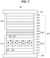
- FIG. 5 is a schematic cross-sectional view illustrating an organic light emitting display device according to a fourth embodiment of the present invention.
- the organic light emitting display device 400 includes a first substrate 410, where a red pixel RP, a green pixel GP and a blue pixel BP are defined, a second substrate 470 facing the first substrate 410, an OLED D, which is positioned between the first and second substrates 410 and 470 and providing white emission, and a color conversion layer 480 between the OLED D and the second substrate 470.
- a color filter may be formed between the second substrate 470 and each color conversion layer 480.
- Each of the first and second substrates 410 and 470 may be a glass substrate or a flexible substrate.
- each of the first and second substrates 410 and 470 may be a polyimide (PI) substrate, a polyethersulfone (PES) substrate, a polyethylenenaphthalate (PEN) substrate, a polyethylene terephthalate (PET) substrate or a polycarbonate (PC) substrate.
- PI polyimide
- PES polyethersulfone
- PEN polyethylenenaphthalate
- PET polyethylene terephthalate
- PC polycarbonate
- the OLED D including a first electrode 460, an organic emitting layer 462 and a second electrode 464 is formed on the planarization layer 450.
- the first electrode 460 may be connected to the drain electrode of the TFT Tr through the drain contact hole 452.
- a bank layer 466 is formed on the planarization layer 450 to cover an edge of the first electrode 460. Namely, the bank layer 466 is positioned at a boundary of the pixel and exposes a center of the first electrode 460 in the pixel.
- the OLED D emits a blue light and may have a structure shown in FIG. 3 or FIG. 4 . Namely, the OLED D is formed in each of the red, green and blue pixels RP, GP and BP and provides the blue light.
- the organic emitting layer 462 of the OLED D includes the blue EML 240 including the first blue emitting layer 250, which is disposed to be closer to the first electrode 160 as an anode, and the second blue emitting layer 260, which is disposed to be closer to the second electrode 164 as a cathode.
- the first blue emitting layer 250 includes the first host 252 and the first dopant 254, and the second blue emitting layer 260 includes the second host 262 and the second dopant 264.
- the first host 252 includes at least one of the first host compounds represented by Formula 1
- the second host 262 includes at least one of the second host compounds represented by Formula 3.
- the first dopant 254 is one of the first compound represented by Formula 5 and the second compound represented by Formula 6, and the second dopant 264 is one of the third compound represented by Formula 5 and the fourth compound represented by Formula 6.
- the color conversion layer 480 includes a first color conversion layer 482 corresponding to the red pixel RP and a second color conversion layer 484 corresponding to the green pixel GP.
- the color conversion layer 480 may include an inorganic color conversion material such as a quantum dot.
- the organic light emitting display device 400 can display a full-color image.
- a color filter layer may be disposed between the second substrate 470 and the color conversion layer 480.
- the color filter layer may include a red color filter and a green color filter respectively corresponding to the red and green pixel regions.
- the color conversion layer 480 is disposed between the OLED D and the first substrate 410.
- the color filter layer may be disposed between the first substrate 410 and the color conversion layer 480.
- An interlayer insulating layer 532 which is formed of an insulating material, is formed on the gate electrode 530.
- the interlayer insulating layer 532 may be formed of an inorganic insulating material, e.g., silicon oxide or silicon nitride, or an organic insulating material, e.g., benzocyclobutene or photo-acryl.
- the semiconductor layer 522, the gate electrode 530, the source electrode 540 and the drain electrode 542 constitute the TFT Tr.
- the TFT Tr serves as a driving element. Namely, the TFT Tr may correspond to the driving TFT Td (of FIG. 1 ).
- the power line which may be formed to be parallel to and spaced apart from one of the gate and data lines, and the storage capacitor for maintaining the voltage of the gate electrode of the TFT Tr in one frame may be further formed.
- a planarization layer 550 which includes a drain contact hole 552 exposing the drain electrode 542 of the TFT Tr, is formed to cover the color filter layer 580 and the TFT Tr.
- a first electrode 560 which is connected to the drain electrode 542 of the TFT Tr through the drain contact hole 552, is separately formed in each pixel and on the planarization layer 550.
- the first electrode 560 may be an anode and may be formed of a conductive material having a relatively high work function.
- the first electrode 560 may be formed of a transparent conductive material, e.g., ITO or IZO.
- a bank layer 566 is formed on the planarization layer 550 to cover an edge of the first electrode 560. Namely, the bank layer 566 is positioned at a boundary of the pixel and exposes a center of the first electrode 560 in the pixel.
- the OLED D3 is positioned to correspond to all of the red, green and blue pixel regions RP, GP and BP.
- the first EML 640 in the first emitting part 610 is a blue EML.
- the first EML 640 includes a first blue emitting layer 620 being closer to the first electrode 560 and a second blue emitting layer 630 being closer to the second electrode 564 and adjacent to the first blue emitting layer 620.
- the second blue emitting layer 630 is disposed between the first blue emitting layer 620 and the second electrode 564 and contacts the first blue emitting layer 620.
- the first EML 640 may have a thickness of 100 to 500 ⁇ .
- a summation of a thickness of the first blue emitting layer 620 and a thickness of the second blue emitting layer 630 is equal to a thickness of the first EML 640, and the thickness of the first blue emitting layer 620 and the thickness of the second blue emitting layer 630 may be same or different.
- Each of the thickness of the first blue emitting layer 620 and the thickness of the second blue emitting layer 630 may be 10 to 250 ⁇ , e.g., 20 to 250 ⁇ .
- the first blue emitting layer 620 includes a first host 622 and a first dopant (e.g., a first emitter) 624.
- the first host 622 may have a weight % (wt%) of 80 to 99.5, preferably 95 to 99.5, and the first dopant 624 may have a wt% of 0.5 to 20, preferably 0.5 to 5.
- the first host 622 includes at least one of the first host compounds, e.g., a pyrene derivative, represented by Formula 1
- the second host 632 includes at least one of the second host compounds, e.g., an anthracene derivative, represented by Formula 3.
- the first host 622 may include at least one of the compounds in Formula 2
- the second host 632 may include at least one of the compounds in Formula 4.
- the first dopant 624 is one of a first compound represented by Formula 5 and a second compound represented by Formula 6, and the second dopant 634 is one of a third compound represented by Formula 5 and a fourth compound represented by Formula 6.
- i) both of the first dopant 624 and the second dopant 634 are represented by Formula 5, and the first dopant 624 and the second dopant 634 are same or different
- ii) the first dopant 624 is represented by Formula 5
- the second dopant 634 is represented by Formula 6
- the first dopant 624 is represented by Formula 6
- the second dopant 634 is represented by Formula 5
- both of the first dopant 624 and the second dopant 634 are represented by Formula 6, and the second dopant 634 is represented by Formula 5, or iv) both of the first dopant 624 and the second dopant 634 are represented by Formula 6, and the first dopant 624 and the second dopant 634 are same or different.
- the first dopant 624 may include one of the compound represented by Formula 5 and the compound represented by Formula 6, and the second dopant 634 may include the other one of the compound represented by Formula 5 and the compound represented by Formula 6.
- the compound represented by Formula 5 may have a weight % of 0.5 to 3
- the compound represented by Formula 6 may have a weight % of 1.5 to 5.
- the first dopant 624 may include the first compound represented by Formula 5, and the second dopant 634 may include the fourth compound represented by Formula 6.
- a weight % of the first dopant 624 in the first blue emitting layer 620 may be smaller than that of the second dopant 634 in the second blue emitting layer 630.
- the first dopant 624 in the first blue emitting layer 620 may have a weight % of 0.5 to 3
- the second dopant 634 in the second blue emitting layer 630 may have a weight % of 1.5 to 5.
- the OLED D3 may have a big advantage in the driving voltage, the emitting efficiency and the lifespan.
- the first dopant 624 may include the second compound represented by Formula 6, and the second dopant 634 may include the third compound represented by Formula 5.
- a weight % of the first dopant 624 in the first blue emitting layer 620 may be greater than that of the second dopant 634 in the second blue emitting layer 630.
- the first dopant 624 in the first blue emitting layer 620 may have a weight % of 1.5 to 5
- the second dopant 634 in the second blue emitting layer 630 may have a weight % of 0.5 to 3.
- the OLED D3 may have a big advantage in the driving voltage, the color purity and the lifespan.
- the first emitting part 610 may further include at least one of a first HTL 613 disposed under the first EML 640 and a first ETL 619 disposed over the first EML 640.
- the first HTL 613 may be disposed between the first EML 640 and the first electrode 560
- the first ETL 619 may be disposed between the first EML 640 and the second electrode 564.
- the first emitting part 610 may further include an HIL 611 between the first HTL 613 and the first electrode 560
- the first emitting part 610 may further include at least one of a first EBL 615 between the first EML 640 and the first HTL 613 and a first HBL 617 between the first EML 640 and the first ETL 619.
- the second EML 680 in the second emitting part 650 may be a yellow-green EML.
- the second EML 680 may include a yellow-green host and a yellow-green dopant.
- the yellow-green dopant may be one of a fluorescent compound, a phosphorescent compound and a delayed fluorescent compound.
- the yellow-green dopant may be selected from the group consisting of 5,6,11,12-tetraphenylnaphthalene (Rubrene), 2,8-di-tert-butyl-5,11-bis(4-tert-butylphenyl)-6,12-diphenyltetracene (TBRb), bis(2-phenylbenzothiazolato)(acetylacetonate)irdium(III) (Ir(BT)2(acac)), bis(2-(9,9-diethytl-fluoren-2-yl)-1-phenyl-1H-benzo[d]imdiazolato)(acetylacetonate)iridium(III) (Ir(fbi)2(acac)), bis(2-phenylpyridine)(3-(pyridine-2-yl)-2H-chromen-2-onate)iridium(III) (fac-Ir(ppy)2Pc),
- the HIL 611 may include the above-mentioned hole injection material and may have a thickness of 10 to 200 ⁇ .
- Each of the first and second ETLs 619 and 657 may include the above-mentioned electron transporting material and may have a thickness of 500 to 1500 ⁇ , preferably 600 to 1000 ⁇ .
- Each of the first and second EBLs 615 and 653 may include the above-mentioned electron blocking material and may have a thickness of 10 to 300 ⁇ .
- the N-type CGL 692 is positioned between the first ETL 619 and the second HTL 651, and the P-type CGL 694 is positioned between the N-type CGL 692 and the second HTL 651.
- the first EML 640 between the first electrode 560 and the CGL 690 may be the yellow-green EML
- the second EML 680 between the second electrode 564 and the CGL 690 may be the blue EML including the first and second blue emitting layers 620 and 630.
- the OLED D4 is positioned to correspond to all of the red, green and blue pixel regions RP, GP and BP.
- the first EML 720 in the first emitting part 710 is a blue EML.
- the first EML 720 includes a first blue emitting layer 722 being closer to the first electrode 560 and a second blue emitting layer 724 being closer to the second electrode 564 and adjacent to the first blue emitting layer 722.
- the second blue emitting layer 724 is disposed between the first blue emitting layer 722 and the second electrode 564 and contacts the first blue emitting layer 722.
- the second blue emitting layer 724 includes a second host 724a and a second dopant (e.g., a second emitter) 724b.
- the second host 724a may have a weight % (wt%) of 80 to 99.5, preferably 95 to 99.5
- the second dopant 724b may have a wt% of 0.5 to 20, preferably 0.5 to 5.
- a weight % of the first host 722a in the first blue emitting layer 722 and a weight % of the second host 724a in the second blue emitting layer 724 may be same or different, and a weight % of the first dopant 722b in the first blue emitting layer 722 and a weight % of the second dopant 724b in the second blue emitting layer 724 may be same or different.
- the first host 722a includes at least one of the first host compounds, e.g., a pyrene derivative, represented by Formula 1, and the second host 724a includes at least one of the second host compounds, e.g., an anthracene derivative, represented by Formula 3.
- the first host 722a may include at least one of the compounds in Formula 2
- the second host 724a may include at least one of the compounds in Formula 4.
- the first dopant 722b may include one of the compound represented by Formula 5 and the compound represented by Formula 6, and the second dopant 724b may include the other one of the compound represented by Formula 5 and the compound represented by Formula 6.
- the compound represented by Formula 5 may have a weight % of 0.5 to 3
- the compound represented by Formula 6 may have a weight % of 1.5 to 5.
- the first dopant 722b may include the first compound represented by Formula 5, and the second dopant 724b may include the fourth compound represented by Formula 6.
- a weight % of the first dopant 722b in the first blue emitting layer 722 may be smaller than that of the second dopant 724b in the second blue emitting layer 724.
- the first dopant 722b in the first blue emitting layer 722 may have a weight % of 0.5 to 3
- the second dopant 724b in the second blue emitting layer 724 may have a weight % of 1.5 to 5.
- the OLED D4 may have a big advantage in the driving voltage, the emitting efficiency and the lifespan.
- the first dopant 722b may include the second compound represented by Formula 6, and the second dopant 724b may include the third compound represented by Formula 5.
- a weight % of the first dopant 722b in the first blue emitting layer 722 may be greater than that of the second dopant 724b in the second blue emitting layer 724.
- the first dopant 722b in the first blue emitting layer 722 may have a weight % of 1.5 to 5
- the second dopant 724b in the second blue emitting layer 724 may have a weight % of 0.5 to 3.
- the OLED D4 may have a big advantage in the driving voltage, the color purity and the lifespan.
- the first emitting part 710 may further include at least one of a first HTL 713 disposed under the first EML 720 and a first ETL 719 disposed over the first EML 720.
- the first HTL 713 may be disposed between the first EML 720 and the first electrode 560
- the first ETL 719 may be disposed between the first EML 720 and the second electrode 564.
- the first emitting part 710 may further include an HIL 711 between the first HTL 713 and the first electrode 560
- the first emitting part 710 may further include at least one of a first EBL 715 between the first EML 720 and the first HTL 713 and a first HBL 717 between the first EML 720 and the first ETL 719.
- the first ETL 719 may have a hole blocking function as well as an electron transporting function so that the first HBL 717 may be omitted.
- the first emitting part 710 has a structure of the HIL 711, the first HTL 713, the first EBL 715, the first bule emitting layer 722, the second blue emitting layer 724 and the first ETL 719 sequentially stacked on the first electrode 560.
- the first blue emitting layer 722 is spaced apart from the first HTL 713 and contacts the first EBL 715, and the second blue emitting layer 724 contacts the first ETL 719.
- the second EML 740 in the second emitting part 730 is a blue EML.
- the second EML 740 includes a third blue emitting layer 742, which is disposed to be closer to the first electrode 560, and a fourth blue emitting layer 744, which is disposed to be closer to the second electrode 564 and is adjacent to the third blue emitting layer 742.
- the fourth blue emitting layer 744 is positioned between the third blue emitting layer 742 and the second electrode 564 and contacts the third blue emitting layer 742.
- the thickness of the third blue emitting layer 742 may be smaller than that of the fourth blue emitting layer 744.
- the third blue emitting layer 742 may have a thickness of 20 to 100 ⁇
- the fourth blue emitting layer 744 may have a thickness of 150 to 250 ⁇ .
- the third dopant 742b may include one of the compound represented by Formula 5 and the compound represented by Formula 6, and the fourth dopant 744b may include the other one of the compound represented by Formula 5 and the compound represented by Formula 6.
- the compound represented by Formula 5 may have a weight % of 0.5 to 3
- the compound represented by Formula 6 may have a weight % of 1.5 to 5.
- the second ETL 737 may have a hole blocking function as well as an electron transporting function so that the second HBL 735 may be omitted.
- the second emitting part 730 has a structure of the second HTL 731, the second EBL 733, the third blue emitting layer 742, the fourth blue emitting layer 744, the second ETL 737 and the EII, 739.
- the third blue emitting layer 742 is spaced apart from the second HTL 731 and contacts the second EBL 733, and the fourth blue emitting layer 744 contacts the second ETL 737.
- the third EML 760 in the third emitting part 750 includes a red emitting layer 762 and a green emitting layer 764 to provide red and green light.
- the green emitting layer 764 may include a green host and a green dopant.
- the green dopant may be one of a fluorescent compound, a phosphorescent compound and a delayed fluorescent compound.
- the third emitting part 750 may further include at least one of a third HTL 751 under the third EML 760 and a third ETL 753 on the third EML 760.
- the third emitting part 750 may further include at least one of a third EBL between the third HTL 751 and the third EML 760 and a third HBL between the third EML 760 and the third ETL 753.
- the HIL 711 may include the above-mentioned hole injection material and may have a thickness of 10 to 200 ⁇ .
- Each of the first to third HTLs 713, 731 and 751 may include the above-mentioned hole transporting material and may have a thickness of 500 to 1500 ⁇ , preferably 600 to 1000 ⁇ .
- Each of the first to third ETLs 719, 737 and 753 may include the above-mentioned electron transporting material and may have a thickness of 100 to 500 ⁇ , preferably 100 to 300 ⁇ .
- the EII, 739 may include the above-mentioned electron injection material and may have a thickness of 5 to 40 ⁇ , preferably 10 to 20 ⁇ .
- Each of the first EBL 715, the second EBL 733 and the third EBL may include the above-mentioned electron blocking material and may have a thickness of 10 to 300 ⁇ .
- Each of the first HBL 717, the second HBL 735 and the third HBL may include the above-mentioned hole blocking material and may have a thickness of 10 to 300 ⁇ .
- the first CGL 770 is positioned between the first and third emitting parts 710 and 750, and the second CGL 780 is positioned between the second and third emitting parts 730 and 750.
- the first and third emitting parts 710 and 750 may be connected to each other through the first CGL 770
- the second and third emitting parts 730 and 750 may be connected to each other through the second CGL 780.
- the first CGL 770 may be a P-N junction CGL of a first N-type CGL 772 and a first P-type CGL 774
- the second CGL 780 may be a P-N junction CGL of a second N-type CGL 782 and a second P-type CGL 784.
- the first N-type CGL 772 is positioned between the first ETL 719 and the third HTL 751
- the first P-type CGL 774 is positioned between the first N-type CGL 772 and the third HTL 751.
- the second N-type CGL 782 is positioned between the third ETL 753 and the second HTL 731
- the second P-type CGL 784 is positioned between the second N-type CGL 782 and the second HTL 731.
- Each of the first and second N-type CGLs 772 and 782 may include the above-mentioned N-type charge generation material, and each of the first and second P-type CGLs 774 and 784 may include the above-mentioned P-type charge generation material.
- one of the first and second EMLs 720 and 740 may have a double-layered structure, while the other one of the first and second EMLs 720 and 740 may have a single-layered structure.
- the other one of the first and second EMLs 720 and 740 may include a blue host and a blue dopant.
- the blue host may be the above-mentioned blue host material
- the blue dopant may be the above-mentioned blue dopant material.
- the OLED D4 of the present invention includes the first emitting part 710 including the first EML 720 (e.g., a first blue EML), the second emitting part 730 including the second EML 740 (e.g., a second blue EML) and the third emitting part 750 including the third EML 760, which includes the red and green emitting layers 762 and 764, and at least one of the first and second blue EMLs 720 and 740 includes a first blue emitting layer including a first host and a first dopant and a second blue emitting layer including a second host and a second dopant.
- the first host includes at least one of the first host compounds represented by Formula 1
- the second host includes at least one of the second host compounds represented by Formula 3.
- the first dopant is one of the first compound represented by Formula 5 and the second compound represented by Formula 6
- the second dopant is one of the third compound represented by Formula 5 and the fourth compound represented by Formula 6.
- the OLED D4 includes the first and second emitting parts 710 and 730 each providing a blue emission and the third emitting part 750 providing a red-green emission such that the OLED D4 can provide a white emission.
- the OLED D4 in FIG. 8 has a three-stack structure including the first, second and third emitting parts 710, 730 and 750.
- the OLED D4 may further include additional emitting part and additional CGL.
- the OLED D5 includes the first electrode 560, the second electrode 564 and the organic emitting layer 562 therebetween, and the organic emitting layer 562 includes a first emitting part 810 including a first EML 820, a second emitting part 830 including a second EML 840, a third emitting part 850 including a third EML 855 and a fourth emitting part 860 including a fourth EML 863.
- the organic emitting layer 562 may further include a first CGL 870 between the first and third emitting parts 810 and 850, a second CGL 880 between the first and fourth emitting parts 810 and 860, and a third CGL 890 between the second and fourth emitting parts 830 and 860.
- the OLED D5 is positioned to correspond to all of the red, green and blue pixel regions RP, GP and BP.
- the first CGL 870 is positioned between the first and third emitting parts 810 and 850
- the second CGL 880 is positioned between the first and fourth emitting parts 810 and 860
- the third CGL 890 is positioned between the second and fourth emitting parts 830 and 860.
- the third emitting part 850, the first CGL 870, the first emitting part 810, the second CGL 880, the fourth emitting part 860, the third CGL 890 and the second emitting part 830 may be sequentially stacked on the first electrode 560.
- the first EML 820 may have a thickness of 100 to 500 ⁇ .
- a summation of a thickness of the first blue emitting layer 822 and a thickness of the second blue emitting layer 824 is equal to a thickness of the first EML 820, and the thickness of the first blue emitting layer 822 and the thickness of the second blue emitting layer 824 may be same or different.
- Each of the thickness of the first blue emitting layer 822 and the thickness of the second blue emitting layer 824 may be 10 to 250 ⁇ , e.g., 20 to 250 ⁇ .
- the first blue emitting layer 822 includes a first host 822a and a first dopant (e.g., a first emitter) 822b.
- the first host 822a may have a weight % (wt%) of 80 to 99.5, preferably 95 to 99.5
- the first dopant 822b may have a wt% of 0.5 to 20, preferably 0.5 to 5.
- the second blue emitting layer 824 includes a second host 824a and a second dopant (e.g., a second emitter) 824b.
- the second host 824a may have a weight % (wt%) of 80 to 99.5, preferably 95 to 99.5
- the second dopant 824b may have a wt% of 0.5 to 20, preferably 0.5 to 5.
- the first dopant 822b may include the first compound represented by Formula 5, and the second dopant 824b may include the fourth compound represented by Formula 6.
- a weight % of the first dopant 822b in the first blue emitting layer 822 may be smaller than that of the second dopant 824b in the second blue emitting layer 824.
- the first dopant 822b in the first blue emitting layer 822 may have a weight % of 0.5 to 3
- the second dopant 824b in the second blue emitting layer 824 may have a weight % of 1.5 to 5.
- the OLED D5 may have a big advantage in the driving voltage, the emitting efficiency and the lifespan.
- the first dopant 822b may include the second compound represented by Formula 6, and the second dopant 824b may include the third compound represented by Formula 5.
- a weight % of the first dopant 822b in the first blue emitting layer 822 may be greater than that of the second dopant 824b in the second blue emitting layer 824.
- the first dopant 822b in the first blue emitting layer 822 may have a weight % of 1.5 to 5
- the second dopant 824b in the second blue emitting layer 824 may have a weight % of 0.5 to 3.
- the OLED D5 may have a big advantage in the driving voltage, the color purity and the lifespan.
- the first emitting part 810 can further include at least one of a first HTL 813 under the first EML 820 and a first ETL 819 on the first EML 820.
- the first HTL 813 can be positioned between the first EML 820 and the first electrode 560
- the first ETL 819 can be positioned between the first EML 820 and the second CGL 880.
- the first emitting part 810 may have a structure including the first HTL 813, the first EBL, the first bule emitting layer 822, the second blue emitting layer 824, the first HBL and the first ETL 819 sequentially stacked over the first electrode 560.
- the first blue emitting layer 822 is spaced apart from the first HTL 813 and contacts the first EBL
- the second blue emitting layer 824 is spaced apparat from the first ETL 819 and contacts the first HBL.
- the first ETL 819 may have a hole blocking function as well as an electron transporting function so that the first HBL may be omitted.
- the first emitting part 810 has a structure of the first HTL 813, the first EBL, the first bule emitting layer 822, the second blue emitting layer 824 and the first ETL 819 sequentially stacked over the first electrode 560.
- the first blue emitting layer 822 is spaced apart from the first HTL 813 and contacts the first EBL
- the second blue emitting layer 824 contacts the first ETL 819.
- the second EML 840 in the second emitting part 830 is a blue EML.
- the second EML 840 includes a third blue emitting layer 842, which is disposed to be closer to the first electrode 560, and a fourth blue emitting layer 844, which is disposed to be closer to the second electrode 564 and is adjacent to the third blue emitting layer 842.
- the fourth blue emitting layer 844 is positioned between the third blue emitting layer 842 and the second electrode 564 and contacts the third blue emitting layer 842.
- the second EML 840 may have a thickness of 100 to 500 ⁇ .
- a summation of a thickness of the third blue emitting layer 842 and a thickness of the fourth blue emitting layer 844 is equal to a thickness of the second EML 840, and the thickness of the third blue emitting layer 842 and the thickness of the fourth blue emitting layer 844 may be same or different.
- Each of the thickness of the third blue emitting layer 842 and the thickness of the fourth blue emitting layer 844 may be 10 to 250 ⁇ , e.g., 20 to 250 ⁇ .
- the thickness of the third blue emitting layer 842 may be smaller than that of the fourth blue emitting layer 844.
- the third blue emitting layer 842 may have a thickness of 20 to 100 ⁇
- the fourth blue emitting layer 844 may have a thickness of 150 to 250 ⁇ .
- the third blue emitting layer 842 includes a third host 842a and a third dopant (e.g., a third emitter) 842b.
- the third host 842a may have a weight % (wt%) of 80 to 99.5, preferably 95 to 99.5, and the third dopant 842b may have a wt% of 0.5 to 20, preferably 0.5 to 5.
- a weight % of the third host 842a in the third blue emitting layer 842 and a weight % of the fourth host 844a in the fourth blue emitting layer 844 may be same or different, and a weight % of the third dopant 842b in the third blue emitting layer 842 and a weight % of the fourth dopant 844b in the fourth blue emitting layer 844 may be same or different.
- the third dopant 842b is one of a first compound represented by Formula 5 and a second compound represented by Formula 6, and the fourth dopant 844b is one of a third compound represented by Formula 5 and a fourth compound represented by Formula 6.
- both of the third dopant 842b and the fourth dopant 844b are represented by Formula 5, and the third dopant 842b and the fourth dopant 844b are same or different
- ii) the third dopant 842b is represented by Formula 5
- the fourth dopant 844b is represented by Formula 6
- the fourth dopant 844b is represented by Formula 6
- the fourth dopant 844b is represented by Formula 5
- both of the third dopant 842b and the fourth dopant 844b are represented by Formula 6, and the third dopant 842b and the fourth dopant 844b are same or different.
- the third dopant 842b may include the first compound represented by Formula 5, and the fourth dopant 844b may include the fourth compound represented by Formula 6.
- a weight % of the third dopant 842b in the third blue emitting layer 842 may be smaller than that of the fourth dopant 844b in the fourth blue emitting layer 844.
- the third dopant 842b in the third blue emitting layer 842 may have a weight % of 0.5 to 3
- the fourth dopant 844b in the fourth blue emitting layer 844 may have a weight % of 1.5 to 5.
- the OLED D5 may have a big advantage in the driving voltage, the emitting efficiency and the lifespan.
- the third dopant 842b may include the second compound represented by Formula 6, and the fourth dopant 844b may include the third compound represented by Formula 5.
- a weight % of the third dopant 842b in the third blue emitting layer 842 may be greater than that of the fourth dopant 844b in the fourth blue emitting layer 844.
- the third dopant 842b in the third blue emitting layer 842 may have a weight % of 1.5 to 5
- the fourth dopant 844b in the fourth blue emitting layer 844 may have a weight % of 0.5 to 3.
- the OLED D5 may have a big advantage in the driving voltage, the color purity and the lifespan.
- the second emitting part 830 may further include at least one of a second HTL 831 disposed under the second EML 840 and a second ETL 837 disposed over the second EML 840. Namely, the second HTL 831 is positioned between the second EML 840 and the first emitting part 810, and the second ETL 837 is positioned between the second EML 840 and the second electrode 564.
- the second emitting part 830 may further include an EIL 839 between the second ETL 837 and the second electrode 564.
- the third EML 855 in the third emitting part 850 may be a red EML.
- the third EML 855 may include a red host and a red dopant.
- the red host may be the above-mentioned red host
- the red dopant may be the above-mentioned red dopant.
- the third emitting part 850 may further include at least one of a third HTL 853 between the third EML 855 and the first electrode 560 and a third ETL 857 disposed between the third EML 855 and the first CGL 870.
- the third emitting part 850 may further include an HIL 851 between the third HTL 853 and the first electrode 560
- the third emitting part 850 may further include at least one of a third EBL between the third EML 855 and the third HTL 853 and a third HBL between the third EML 855 and the third ETL 857.
- the fourth EML 863 in the fourth emitting part 860 may be a green EML.
- the fourth EML 863 may include a green host and a green dopant.
- the green host may be the above-mentioned green host, and the green dopant may be the above-mentioned green dopant.
- the fourth emitting part 860 may further include at least one of a fourth HTL 861 between the fourth EML 863 and the second CGL 880 and a fourth ETL 865 between the fourth EML 863 and the third CGL 890.
- the compound BH1-1 in Formula 2 was used as the first host, the compounds BD2-1, BD2-2 and BD2-3 in Formula 8 were used as the first dopant.
- the compound BH2-1 in in Formula 4 was used as the second host, and the compound BD1-1 in Formula 7 was used as the second dopant.
- the OLED has big advantage in the driving voltage, the color purity and the lifespan with sufficient emitting efficiency.
- the compound BH1-2 in Formula 2 was used as the first host to form the first blue emitting layer (50 ⁇ ), and the compound BH2-1 in Formula 4 was used as the second host to form the second blue emitting layer (200 ⁇ ).
Landscapes
- Chemical & Material Sciences (AREA)
- Engineering & Computer Science (AREA)
- Materials Engineering (AREA)
- Physics & Mathematics (AREA)
- Spectroscopy & Molecular Physics (AREA)
- Optics & Photonics (AREA)
- Organic Chemistry (AREA)
- Inorganic Chemistry (AREA)
- Microelectronics & Electronic Packaging (AREA)
- Electroluminescent Light Sources (AREA)
Abstract
Description
- The present invention relates to an organic light emitting device, and more specifically, to an organic light emitting diode (OLED) having advantages in at least one of driving voltage, emitting efficiency and lifespan and an organic light emitting device including the same.
- As requests for a flat panel display device having a small occupied area have been increased, an organic light emitting display device including an OLED has been the subject of recent research and development.
- The OLED emits light by injecting electrons from a cathode as an electron injection electrode and holes from an anode as a hole injection electrode into an emitting material layer (EML), combining the electrons with the holes, generating an exciton, and transforming the exciton from an excited state to a ground state. A flexible substrate, for example, a plastic substrate, can be used as a base substrate where elements are formed. In addition, the organic light emitting display device can be operated at a voltage (e.g., 10V or below) lower than a voltage required to operate other display devices. Moreover, the organic light emitting display device has advantages in the power consumption and the color sense.
- The OLED includes a fist electrode as an anode over a substrate, a second electrode, which is spaced apart from and faces the first electrode, and an organic emitting layer therebetween.
- For example, the organic light emitting display device may include a red pixel region, a green pixel region and a blue pixel region, and the OLED may be formed in each of the red, green and blue pixel regions.
- However, the OLED in the blue pixel does not provide sufficient emitting efficiency, color purity and lifespan such that the organic light emitting display device has a limitation in the emitting efficiency, the color purity and the lifespan.
- The present invention is directed to an OLED and an organic light emitting device including the OLED that substantially obviate one or more of the problems associated with the limitations and disadvantages of the related conventional art.
- Additional features and advantages of the present invention are set forth in the description which follows, and will be apparent from the description, or evident by practice of the present invention. The objectives and other advantages of the present invention are realized and attained by the features described herein as well as in the appended drawings.
- To achieve these and other advantages in accordance with the purpose of the embodiments of the present invention, as described herein, an aspect of the present invention is an organic light emitting diode comprising a first electrode; a second electrode facing the first electrode; and a first emitting part including a first blue emitting layer and a second blue emitting layer and positioned between the first and second electrodes, the second blue emitting layer positioned between the first blue emitting layer and the second electrode and contacting the first blue emitting layer, wherein the first blue emitting layer includes a first host and a first dopant, and the second blue emitting layer includes a second host and a second dopant, wherein the first host is a pyrene derivative, and the second host is an anthracene derivative, wherein the first dopant is a first compound represented by Formula 5 or a second compound represented by Formula 6, and the second dopant is a third compound represented by Formula 5 or a fourth compound represented by Formula 6,

- each of e1 and e2 is independently an integer of 0 to 4, and e3 is an integer of 0 to 3,
- each of Ar21 and Ar22 is independently selected from the group consisting of a substituted or unsubstituted C6 to C30 arylamino group, a substituted or unsubstituted C6 to C30 aryl group, a substituted or unsubstituted C3 to C30 heteroaryl group and a substituted or unsubstituted C6 to C30 alicyclic group, and R21, R22 and R23 is independently selected from the group consisting of a substituted or unsubstituted C1 to C30 alkyl group, a substituted or unsubstituted C3 to C30 cycloalkyl group, a substituted or unsubstituted C6 to C30 arylamino group, a substituted or unsubstituted C6 to C30 aryl group and a substituted or unsubstituted C3 to C30 heteroaryl group,
- In an embodiment,when the first dopant is the first compound and the second dopant is the fourth compound, a weight % of the first dopant in the first blue emitting material layer is smaller than a weight % of the second dopant in the second blue emitting material layer, or wherein when the first dopant is the second compound and the second dopant is the third compound, a weight % of the first dopant in the first blue emitting material layer is greater than a weight % of the second dopant in the second blue emitting material layer.
In an embodiment, each of the first compound and the third compound is independently one of compounds in Formula 7:


Formula 1, - each of a1 and a2 is independently 0 or 1, and a3 is an integer of 0 to 4,
- R1 is selected from the group consisting of deuterium, a substituted or unsubstituted C1 to C30 alkyl group, a substituted or unsubstituted C1 to C30 alkoxy group, a substituted or unsubstituted C6 to C30 aryl group and a substituted or unsubstituted C3 to C30 heteroaryl group,
- each of Ar1 and Ar2 is independently selected from the group consisting of hydrogen, deuterium, a substituted or unsubstituted C6 to C30 aryl group and a substituted or unsubstituted C3 to C30 heteroaryl group, and
- each of L1 and L2 is independently selected from the group consisting of a substituted or unsubstituted C6 to C30 arylene group and a substituted or unsubstituted C3 to C30 heteroarylene group.
- each of b1 and b2 is independently 0 or 1, and b3 is an integer of 0 to 8,
- R11 is selected from the group consisting of deuterium, a substituted or unsubstituted C1 to C30 alkyl group, a substituted or unsubstituted C1 to C30 alkoxy group, a substituted or unsubstituted C6 to C30 aryl group and a substituted or unsubstituted C3 to C30 heteroaryl group,
- each of L11 and L12 is independently selected from the group consisting of a substituted or unsubstituted C6 to C30 arylene group and a substituted or unsubstituted C3 to C30 heteroarylene group, and
- each of Ar11 and Ar12 is independently selected from the group consisting of a substituted or unsubstituted C6 to C30 aryl group and a substituted or unsubstituted C3 to C30 heteroaryl group.
- wherein the third blue emitting layer includes a third host and a third dopant, and the fourth blue emitting layer includes a fourth host and a fourth dopant,
- wherein the third host is the pyrene derivative, and the fourth host is the anthracene derivative, wherein the third dopant is a fifth compound represented by the Formula 5 or a sixth compound represented by the Formula 6, and the second dopant is a seventh compound represented by the Formula 5 or an eighth compound represented by the Formula 6.
- In an embodiment, wherein when the third dopant is the fifth compound and the fourth dopant is the eighth compound, a weight % of the third dopant in the third blue emitting material layer is smaller than a weight % of the fourth dopant in the fourth blue emitting material layer, or wherein when the third dopant is the sixth compound and the second dopant is the seventh compound, a weight % of the third dopant in the third blue emitting material layer is greater than a weight % of the fourth dopant in the fourth blue emitting material layer. In an embodiment, the third host is represented by Formula 1:

- each of a1 and a2 is independently 0 or 1, and a3 is an integer of 0 to 4,
- R1 is selected from the group consisting of deuterium, a substituted or unsubstituted C1 to C30 alkyl group, a substituted or unsubstituted C1 to C30 alkoxy group, a substituted or unsubstituted C6 to C30 aryl group and a substituted or unsubstituted C3 to C30 heteroaryl group,
- each of Ar1 and Ar2 is independently selected from the group consisting of hydrogen, deuterium, a substituted or unsubstituted C6 to C30 aryl group and a substituted or unsubstituted C3 to C30 heteroaryl group, and
- each of L1 and L2 is independently selected from the group consisting of a substituted or unsubstituted C6 to C30 arylene group and a substituted or unsubstituted C3 to C30 heteroarylene group.
- each of b1 and b2 is independently 0 or 1, and b3 is an integer of 0 to 8,
- R11 is selected from the group consisting of deuterium, a substituted or unsubstituted C1 to C30 alkyl group, a substituted or unsubstituted C1 to C30 alkoxy group, a substituted or unsubstituted C6 to C30 aryl group and a substituted or unsubstituted C3 to C30 heteroaryl group,
- each of L11 and L12 is independently selected from the group consisting of a substituted or unsubstituted C6 to C30 arylene group and a substituted or unsubstituted C3 to C30 heteroarylene group, and
- each of Ar11 and Ar12 is independently selected from the group consisting of a substituted or unsubstituted C6 to C30 aryl group and a substituted or unsubstituted C3 to C30 heteroaryl group.
- a third emitting part including a red emitting layer and positioned between the first emitting part and the first electrode; and
- a fourth emitting part including a green emitting layer and positioned between the first and second emitting parts.
- Another aspect of the present invention is an organic light emitting device comprising a substrate; the organic light emitting of the invention -diode over the substrate; and an encapsulation layer covering the organic light emitting diode.
- It is to be understood that both the foregoing general description and the following detailed description are exemplary and explanatory and are intended to further explain the present invention as claimed.
- The accompanying drawings, which are included to provide a further understanding of the present invention and are incorporated in and constitute a part of this specification, illustrate embodiments of the present invention and together with the description serve to explain the principles of the present invention.
-
FIG. 1 is a schematic circuit diagram illustrating an organic light emitting display device of the present invention. -
FIG. 2 is a schematic cross-sectional view illustrating an organic light emitting display device according to a first embodiment of the present invention. -
FIG. 3 is a schematic cross-sectional view illustrating an OLED according to a second embodiment of the present invention. -
FIG. 4 is a schematic cross-sectional view illustrating an OLED according to a third embodiment of the present invention. -
FIG. 5 is a schematic cross-sectional view illustrating an organic light emitting display device according to a fourth embodiment of the present invention. -
FIG. 6 is a schematic cross-sectional view illustrating an organic light emitting display device according to a fifth embodiment of the present invention. -
FIG. 7 is a schematic cross-sectional view illustrating an OLED according to a sixth embodiment of the present invention. -
FIG. 8 is a schematic cross-sectional view illustrating an OLED according to a seventh embodiment of the present invention. -
FIG. 9 is a schematic cross-sectional view illustrating an OLED according to an eighth embodiment. - Reference will now be made in detail to aspects of the present invention, examples of which may be illustrated in the accompanying drawings. In the following description, when a detailed description of well-known functions or configurations related to this document is determined to unnecessarily cloud a gist of the inventive concept, the detailed description thereof will be omitted. The progression of processing steps and/or operations described is an example; however, the sequence of steps and/or operations is not limited to that set forth herein and may be changed as is known in the art, with the exception of steps and/or operations necessarily occurring in a particular order. Like reference numerals designate like elements throughout. Names of the respective elements used in the following explanations are selected only for convenience of writing the specification and may be thus different from those used in actual products.
- Advantages and features of the present invention and methods of achieving them will be apparent with reference to the aspects described below in detail with the accompanying drawings. However, the present invention is not limited to the aspects disclosed below, but can be realized in a variety of different forms, and only these aspects allow the disclosure of the present invention to be complete. The present disclosure is provided to fully inform the scope of the invention to the skilled in the art.
- The shapes, sizes, proportions, angles, numbers, and the like disclosed in the drawings for explaining the aspects of the present invention are illustrative, and the present invention is not limited to the illustrated matters. The same reference numerals refer to the same elements throughout the specification. In addition, in describing the present invention, if it is determined that a detailed description of the related known technology unnecessarily obscure the subject matter of the present invention, the detailed description thereof can be omitted. When 'including', 'having', 'consisting', and the like are used in this specification, other parts may be added unless 'only' is used. When a component is expressed in the singular, cases including the plural are included unless specific statement is described.
- In construing an element, the element is construed as including an error or tolerance range although there is no explicit description of such an error or tolerance range.
- In describing a position relationship, for example, when a position relation between two parts is described as, for example, "on," "over," "under," and "next," one or more other parts may be disposed between the two parts unless a more limiting term, such as "just" or "direct(ly)" is used.
- In describing a time relationship, for example, when the temporal order is described as, for example, "after," "subsequent," "next," and "before," a case that is not continuous may be included unless a more limiting term, such as "just," "immediate(ly)," or "direct(ly)" is used.
- It will be understood that, although the terms "first," "second," etc. may be used herein to describe various elements, these elements should not be limited by these terms. These terms are only used to distinguish one element from another. For example, a first element could be termed a second element, and, similarly, a second element could be termed a first element, without departing from the scope of the present invention.
- Features of various aspects of the present invention may be partially or overall coupled to or combined with each other, and may be variously inter-operated with each other and driven technically as those skilled in the art can sufficiently understand. The aspects of the present invention may be carried out independently from each other, or may be carried out together in co-dependent relationship.
- Reference will now be made in detail to some of the examples and preferred embodiments, which are illustrated in the accompanying drawings.
- In the present invention, an organic light emitting device including the OLED may be an organic light emitting display device or an organic lightening device. As an example, an organic light emitting display device, which is a display device including the OLED of the present invention, will be mainly described.
-
FIG. 1 is a schematic circuit diagram illustrating an organic light emitting display device of the present invention. - As illustrated in
FIG. 1 , a gate line GL and a data line DL, which cross each other to define a pixel region (pixel) P, and a power line PL are formed in an organic light emitting display device. A switching thin film transistor (TFT) Ts, a driving TFT Td, a storage capacitor Cst and an OLED D are formed in the pixel region P. The pixel region P may include a red pixel region, a green pixel region and a blue pixel region. - The switching thin film transistor Ts is connected to the gate line GL and the data line DL, and the driving thin film transistor Td is connected between the switching thin film transistor Ts and the power line PL. The storage capacitor Cst is connected to a gate electrode and a drain electrode of the driving TFT Td, and the OLED D is connected to the driving thin film transistor Td.
- When the switching thin film transistor Ts is turned on by the gate signal applied through the gate line GL, the data signal applied through the data line DL is applied into a gate electrode of the driving thin film transistor Td and one electrode of the storage capacitor Cst through the switching thin film transistor Ts.
- The driving thin film transistor Td is turned on by the data signal applied into the gate electrode so that a current proportional to the data signal is supplied from the power line PL to the OLED D through the driving thin film transistor Td. The OLED D emits light having a luminance proportional to the current flowing through the driving thin film transistor Td. In this case, the storage capacitor Cst is charge with a voltage proportional to the data signal so that the voltage of the gate electrode in the driving thin film transistor Td is kept constant during one frame. Therefore, the organic light emitting display device can display a desired image.
-
FIG. 2 is a schematic cross-sectional view illustrating an organic light emitting display device according to a first embodiment of the present invention. - As illustrated in
FIG. 2 , the organic light emittingdisplay device 100 includes asubstrate 110, a TFT Tr and an OLED D disposed on a planarization layer and connected to the TFT Tr. - The
substrate 110 may be a glass substrate or a flexible substrate. For example, the flexible substrate may be a polyimide (PI) substrate, a polyethersulfone (PES) substrate, a polyethylenenaphthalate (PEN) substrate, a polyethylene terephthalate (PET) substrate or a polycarbonate (PC) substrate. - A
buffer layer 120 is formed on the substrate, and the TFT Tr is formed on thebuffer layer 120. Thebuffer layer 120 may be omitted. - A
semiconductor layer 122 is formed on thebuffer layer 120. Thesemiconductor layer 122 may include an oxide semiconductor material or polycrystalline silicon. When thesemiconductor layer 122 includes the oxide semiconductor material, a light-shielding pattern (not shown) may be formed under thesemiconductor layer 122. The light to thesemiconductor layer 122 is shielded or blocked by the light-shielding pattern such that thermal degradation of thesemiconductor layer 122 can be prevented. On the other hand, when thesemiconductor layer 122 includes polycrystalline silicon, impurities may be doped into both sides of thesemiconductor layer 122. - A
gate insulating layer 124 is formed on thesemiconductor layer 122. Thegate insulating layer 124 may be formed of an inorganic insulating material such as silicon oxide (SiOx) or silicon nitride (SiNx). - A
gate electrode 130, which is formed of a conductive material, e.g., metal, is formed on thegate insulating layer 124 to correspond to a center of thesemiconductor layer 122. InFIG. 2 , thegate insulating layer 124 is formed on an entire surface of thesubstrate 110. Alternatively, thegate insulating layer 124 may be patterned to have the same shape as thegate electrode 130. - An interlayer insulating
layer 132, which is formed of an insulating material, is formed on thegate electrode 130. The interlayer insulatinglayer 132 may be formed of an inorganic insulating material, e.g., silicon oxide or silicon nitride, or an organic insulating material, e.g., benzocyclobutene or photo-acryl. - The interlayer insulating
layer 132 includes first and second contact holes 134 and 136 exposing both sides of thesemiconductor layer 122. The first and second contact holes 134 and 136 are positioned at both sides of thegate electrode 130 to be spaced apart from thegate electrode 130. The first and second contact holes 134 and 136 are formed through thegate insulating layer 124 and the interlayer insulatinglayer 132. Alternatively, when thegate insulating layer 124 is patterned to have the same shape as thegate electrode 130, the first and second contact holes 134 and 136 is formed only through the interlayer insulatinglayer 132. - A
source electrode 140 and adrain electrode 142, which are formed of a conductive material, e.g., metal, are formed on theinterlayer insulating layer 132. Thesource electrode 140 and thedrain electrode 142 are spaced apart from each other with respect to thegate electrode 130 and respectively contact both sides of thesemiconductor layer 122 through the first and second contact holes 134 and 136. - The
semiconductor layer 122, thegate electrode 130, thesource electrode 140 and thedrain electrode 142 constitute the TFT Tr. The TFT Tr serves as a driving element. Namely, the TFT Tr may correspond to the driving TFT Td (ofFIG. 1 ). - In the TFT Tr, the
gate electrode 130, thesource electrode 140, and thedrain electrode 142 are positioned over thesemiconductor layer 122. Namely, the TFT Tr has a coplanar structure. Alternatively, in the TFT Tr, the gate electrode may be positioned under the semiconductor layer, and the source and drain electrodes may be positioned over the semiconductor layer such that the TFT Tr may have an inverted staggered structure. In this instance, the semiconductor layer may include amorphous silicon. - Although not shown, the gate line and the data line cross each other to define the pixel region, and the switching TFT is formed to be connected to the gate and data lines. The switching TFT is connected to the TFT Tr as the driving element. In addition, the power line, which may be formed to be parallel to and spaced apart from one of the gate and data lines, and the storage capacitor for maintaining the voltage of the gate electrode of the TFT Tr in one frame may be further formed.
- A
planarization layer 150 is formed on the source and drainelectrodes substrate 110. Theplanarization layer 150 has a flat top surface and includes adrain contact hole 152 exposing thedrain electrode 142 of the TFT Tr. - The OLED D is disposed on the
planarization layer 150 and includes afirst electrode 160, which is connected to thedrain electrode 142 of the TFT Tr, an organic emittinglayer 162 on thefirst electrode 160 and asecond electrode 164 on the organic emittinglayer 162. The OLED D is disposed at each of the red, green and blue pixel regions and emits red light, green light and blue light in the red, green and blue pixel regions, respectively. - The
first electrode 160 is separately formed in each pixel region. Thefirst electrode 160 may be an anode and may be formed of a conductive material having a relatively high work function. For example, thefirst electrode 160 may be formed of a conductive material having a relatively high work function, e.g., a transparent conductive oxide (TCO). for example, thefirst electrode 160 may include at least one of indium-tin-oxide (ITO), indium-zinc-oxide (IZO), indium-tin-zinc oxide (ITZO), tin oxide (SnO), zinc oxide (ZnO), indium-copper-oxide (ICO) and aluminum-zinc-oxide (Al:ZnO, AZO). - When the organic light emitting
display device 100 is operated in a bottom-emission type, thefirst electrode 160 may have a single-layered structure formed of the transparent conductive oxide. Alternatively, when the organic light emittingdisplay device 100 is operated in a top-emission type, thefirst electrode 160 may further include a reflective layer to have a double-layered structure or a triple-layered structure. For example, the reflective layer may include silver (Ag) or aluminum-palladium-copper alloy (APC). In the top-emission type OLED D, thefirst electrode 160 may have a double-layered structure of Ag/ITO or APC/ITO or a triple-layered structure of ITO/Ag/ITO or ITO/APC/ITO. - A
bank layer 166 is formed on theplanarization layer 150 to cover an edge of thefirst electrode 160. Namely, thebank layer 166 is positioned at a boundary of the pixel region and exposes a center of thefirst electrode 160 in the pixel region. - An organic emitting
layer 162 is formed on thefirst electrode 160. The organic emittinglayer 162 may have a single-layered structure of an emitting material layer (EML). Alternatively, the organic emittinglayer 162 may further include at least one of a hole injection layer (HIL), a hole transport layer (HTL), an electron blocking layer (EBL), a hole blocking layer (HBL), an electron transport layer (ETL) and an electron injection layer (EIL) to have a multi-layered structure. - In the blue pixel region, the organic emitting
layer 162 of the OLED D includes a blue EML, and the blue EML includes a first blue emitting layer and a second blue emitting layer. - The first blue emitting layer includes a first host being a pyrene derivative (or compound) and a first dopant being one of a first compound represented by Formula 5 and a second compound represented by Formula 6, and the second blue emitting layer includes a second host being an anthracene derivative and a second dopant being one of a third compound represented by Formula 5 and a fourth compound represented by Formula 6. As a result, the OLED D and the organic light emitting
display device 100 have an advantage in at least one of the driving voltage, the color purity, the emitting efficiency, and the lifespan. - The organic emitting
layer 162 may include two or more blue EMLs, which are disposed to be spaced apart from each other, so that the OLED D may have a tandem structure. - The
second electrode 164 is formed over thesubstrate 110 where the organic emittinglayer 162 is formed. Thesecond electrode 164 covers an entire surface of the display area and may be formed of a conductive material having a relatively low work function to serve as a cathode. For example, thesecond electrode 164 may be formed of a material having high reflectance, such as aluminum (Al), magnesium (Mg), calcium (Ca), silver (Ag), their alloys or their combinations. In the top-emission type organic light emittingdisplay device 100, thesecond electrode 164 may have a thin profile (small thickness) to provide a light transmittance property (or a semi-transmittance property). - An encapsulation layer (or encapsulation film) 170 is formed on the
second electrode 164 to prevent penetration of moisture into the OLED D. Theencapsulation film 170 includes a first inorganic insulatinglayer 172, an organic insulatinglayer 174 and a second inorganic insulatinglayer 176 sequentially stacked, but it is not limited thereto. Theencapsulation film 170 may be omitted. - In the bottom-emission type organic light emitting
display device 100, a metal plate may be disposed on theencapsulation layer 170. - The organic light emitting
display device 100 may include a color filter layer corresponding to the red, green and blue pixel regions. The color filter layer may include red, green and blue color filters respectively corresponding to the red, green and blue pixel regions. The organic light emittingdisplay device 100 with the color filter layer may have improved color purity. - In the bottom-emission type organic light emitting
display device 100, the color filter layer may be disposed between the OLED D and thesubstrate 110, e.g., between the interlayer insulatinglayer 132 and theplanarization layer 150. In the top-emission type organic light emittingdisplay device 100, the color filter layer may be disposed over the OLED D, e.g., on or over thesecond electrode 164 or theencapsulation layer 170. - The organic light emitting
display device 100 may further include a polarization plate for reducing an ambient light reflection. For example, the polarization plate may be a circular polarization plate. In the bottom-emission type organic light emittingdisplay device 100, the polarization plate may be disposed under thesubstrate 110. In the top-emission type organic light emittingdisplay device 100, the polarization plate may be disposed on or over theencapsulation film 170. - In addition, in the top-emission type organic light emitting
display device 100, a cover window may be attached to theencapsulation film 170 or the polarization plate. In this instance, thesubstrate 110 and the cover window have a flexible property such that a flexible organic light emitting display device may be provided. -
FIG. 3 is a schematic cross-sectional view illustrating an OLED according to a second embodiment of the present invention. - As illustrated in
FIG. 3 , the OLED D1 includes the first andsecond electrodes layer 162 therebetween, and the organic emittinglayer 162 includes ablue EML 240. - The organic light emitting display device 100 (of
FIG. 2 ) includes red, green and blue pixels. In addition, the organic light emittingdisplay device 100 may further include a white pixel region. The OLED D1 may be positioned in the blue pixel. - The organic emitting
layer 162 in the red pixel region includes a red EML, and the organic emittinglayer 162 in the green pixel region includes a green EML. - One of the first and
second electrodes second electrodes second electrodes second electrodes - For example, the
first electrode 160 may include a transparent conductive material layer of ITO or IZO, and thesecond electrode 164 may be formed of one of Al, Mg, Ag, AlMg and MgAg. - The
blue EML 240 includes a first blue emittinglayer 250 being closer to thefirst electrode 160 and a second blue emittinglayer 260 being closer to thesecond electrode 164 and adjacent to the first blue emittinglayer 250. Namely, the second blue emittinglayer 260 is disposed between the first blue emittinglayer 250 and thesecond electrode 164 and contacts the first blue emittinglayer 250. - The
blue EML 240 may have a thickness of 100 to 500Å. A summation of a thickness of the first blue emittinglayer 250 and a thickness of the second blue emittinglayer 260 is equal to a thickness of theblue EML 240, and the thickness of the first blue emittinglayer 250 and the thickness of the second blue emittinglayer 260 may be same or different. Each of the thickness of the first blue emittinglayer 250 and the thickness of the second blue emittinglayer 260 may be 10 to 250 Â, e.g., 20 to 250 Å. - In an aspect of the present invention, the thickness of the first blue emitting
layer 250 may be smaller than that of the second blue emittinglayer 260. For example, the first blue emittinglayer 250 may have a thickness of 20 to 100 Â, and the second blue emittinglayer 260 may have a thickness of 150 to 250 Å. - The first blue emitting
layer 250 includes a first host 252 and a first dopant (e.g., a first emitter) 254. In the first blue emittinglayer 250, the first host 252 may have a weight % (wt%) of 80 to 99.5, preferably 95 to 99.5, and thefirst dopant 254 may have a wt% of 0.5 to 20, preferably 0.5 to 5. - The second blue emitting
layer 260 includes asecond host 262 and a second dopant (e.g., a second emitter) 264. In the second blue emittinglayer 260, thesecond host 262 may have a weight % (wt%) of 80 to 99.5, preferably 95 to 99.5, and thesecond dopant 264 may have a wt% of 0.5 to 20, preferably 0.5 to 5. - A weight % of the first host 252 in the first blue emitting
layer 250 and a weight % of thesecond host 262 in the second blue emittinglayer 260 may be same or different, and a weight % of thefirst dopant 254 in the first blue emittinglayer 250 and a weight % of thesecond dopant 264 in the second blue emittinglayer 260 may be same or different. - The first host 252 includes at least one of a first host compound, i.e., a pyrene derivative, preferably represented by
Formula 1.
- In
Formula 1, each of a1 and a2 is independently 0 or 1, and a3 is an integer of 0 to 4, - R1 is selected from the group consisting of deuterium, a substituted or unsubstituted C1 to C30 alkyl group, a substituted or unsubstituted C1 to C30 alkoxy group, a substituted or unsubstituted C6 to C30 aryl group and a substituted or unsubstituted C3 to C30 heteroaryl group,
- each of Ar1 and Ar2 is independently selected from the group consisting of hydrogen, deuterium, a substituted or unsubstituted C6 to C30 aryl group and a substituted or unsubstituted C3 to C30 heteroaryl group, and
- each of L1 and L2 is independently selected from the group consisting of a substituted or unsubstituted C6 to C30 arylene group and a substituted or unsubstituted C3 to C30 heteroarylene group.
- In the present invention, without specific definition, a substituent of an alkyl group, an alkoxy group, a cycloalkyl group, an alicylic group, an aryamino group, an aryl group and a heteroaryl group may be at least one of deuterium, halogen, cyano, a substituted or unsubstituted C1 to C10 alkyl group, a substituted or unsubstituted C3 to C30 cycloalkyl group, a substituted or unsubstituted C6 to C30 arylamino group, a substituted or unsubstituted C6 to C30 aryl group and a substituted or unsubstituted C3 to C30 heteroaryl group.
- In the present invention, without specific definition, a C1 to C30 alkyl group may be selected from the group consisting of methyl, ethyl, propyl and butyl, e.g., tert-butyl or isobutyl.
- In the present invention, without specific definition, a C3 to C30 cycloalkyl group may be selected from the group consisting of cyclopropyl, cyclobutyl, cyclopentyl, cyclohexyl, and adamantanyl.
- In the present invention, without specific definition, a C6 to C30 alicyclic group may be selected from the group consisting of tetralinyl, methyltetralinyl, ethyltetralinyl, tetramethyltetralinyl and pentamethylindanyl.
- In the present invention, without specific definition, a C6 to C30 aryl group may be selected from the group consisting of phenyl, biphenyl, terphenyl, naphthyl, anthracenyl, pentalenyl, indenyl, indenoindenyl, heptalenyl, biphenylenyl, indacenyl, phenanthrenyl, benzophenanthrenyl, dibenzophenanthrenyl, azulenyl, pyrenyl, fluoranthenyl, triphenylenyl, chrysenyl, tetraphenyl, tetrasenyl, picenyl, pentaphenyl, pentacenyl, fluorenyl, indenofluorenyl and spiro-fluorenyl.
- In the present invention, without specific definition, a C6 to C30 arylene group may be selected from the group consisting of phenylene, biphenylene, terphenylene, naphthylene, anthracenylene, pentanenylene, indenylene, indenoindenylene, heptalenylene, biphenylenylene, indacenylene, phenanthrenylene, benzophenanthrenylene, dibenzophenanthrenylene, azulenylene, pyrenylene, fluoranthenylene, triphenylenylene, chrysenylene, tetraphenylene, tetrasenylene, picenylene, pentaphenylene, pentacenylene, fluorenylene, indenofluorenylene and spiro-fluorenylene.
- In the present disclosure, without specific definition, a C3 to C30 heteroaryl group can be selected from the group consisting of pyrrolyl, pyridinyl, pyrimidinyl, pyrazinyl, pyridazinyl, triazinyl, tetrazinyl, imidazolyl, pyrazolyl, indolyl, isoindolyl, indazolyl, indolizinyl, pyrrolizinyl, carbazolyl, benzocarbazolyl, dibenzocarbazolyl, indolocarbazolyl, indenocarbazolyl, benzofurocarbazolyl, benzothienocarbazolyl, quinolinyl, isoquinolinyl, phthalazinyl, quinoxalinyl, cinnolinyl, quinazolinyl, quinolizinyl, quinolinyl, purinyl, phthalazinyl, quinoxalinyl, benzoquinolinyl, benzoisoquinolinyl, benzoquinazolinyl, benzoquinoxalinyl, acridinyl, phenanthrolinyl, perimidinyl, phenanthridinyl, pteridinyl, cinnolinyl, naphtharidinyl, furanyl, oxazinyl, oxazolyl, oxadiazolyl, triazolyl, dioxinyl, benzofuranyl, dibenzofuranyl, thiopyranyl, xanthenyl, chromanyl, isochromanyl, thioazinyl, thiophenyl, benzothiophenyl, dibenzothiophenyl, difuropyrazinyl, benzofurodibenzofuranyl, benzothienobenzothiophenyl, benzothienodibenzothiophenyl, benzothienobenzofuranyl, and benzothienodibenzofuranyl.
- In the present disclosure, without specific definition, a C3 to C30 heteroarylene group can be selected from the group consisting of pyrrolylene, pyridinylv, pyrimidinylene, pyrazinylene, pyridazinylene, triazinylene, tetrazinylene, imidazolylene, pyrazolylene, indolylene, isoindolylene, indazolylene, indolizinylene, pyrrolizinylene, carbazolylene, benzocarbazolylene, dibenzocarbazolylene, indolocarbazolylene, indenocarbazolylene, benzofurocarbazolylene, benzothienocarbazolylene, quinolinylene, isoquinolinylene, phthalazinylene, quinoxalinylene, cinnolinylene, quinazolinylene, quinolizinyl, quinolinylene, purinylene, phthalazinylene, quinoxalinylene, benzoquinolinylene, benzoisoquinolinylene, benzoquinazolinylene, benzoquinoxalinylene, acridinylene, phenanthrolinylene, perimidinylene, phenanthridinylene, pteridinylene, cinnolinylene, naphtharidinylene, furanylene, oxazinylene, oxazolylene, oxadiazolylene, triazolylene, dioxinylene, benzofuranyenel, dibenzofuranylene, thiopyranylene, xanthenylene, chromanylene, isochromanylene, thioazinylene, thiophenylene, benzothiophenylene, dibenzothiophenylene, difuropyrazinyl ene, benzofurodibenzofuranylene, benzothienobenzothiophenylene, benzothienodibenzothiophenylene, benzothienobenzofuranylene, and benzothienodibenzofuranylene.
- In
Formula 1, a3 may be 0 (zero). - In
Formula 1, each of Ar1 and Ar2 may be independently selected from the group consisting of hydrogen, a C6 to C30 aryl group, e.g., phenyl, naphthyl, fluorenyl, phenanthrenyl or pyrenyl, unsubstituted or substituted with at least one of a C1 to C10 alkyl group and a C6 to C30 aryl group, and a C3 to C30 heteroaryl group, e.g., dibenzothiophenyl, benzo[b]naphto[1,2-d]furanyl, or benzo[b]naphto[2,3-d]furanyl, unsubstituted or substituted with at least one of a C1 to C10 alkyl group and a C6 to C30 aryl group. - In
Formula 1, each of L1 and L2 may be independently a substituted or unsubstituted C6 to C30 arylene group, e.g., phenylene. - In
Formula 1, each of a1 and a2 may be 0 (zero), and a bonding site of Ar1 and Ar2 may be specified. For example,Formula 1 may be represented by Formula 1a or 1b.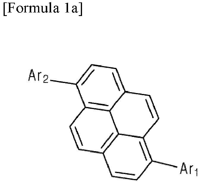
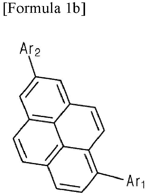
- In each of Formulas 1a and 1b, the definitions of Ar1 and Ar2 are same as those in
Formula 1. - For example, the first host 252 included in the first
blue EML 250 may include at least one of compounds in Formula 2as referred to herein above. - The
second host 262 includes at least one of a second host compound, i.e., an anthracene derivative, preferably represented byFormula 3.
- In
Formula 3, each of b1 and b2 is independently 0 or 1, and b3 is an integer of 0 to 8, - R11 is selected from the group consisting of deuterium, a substituted or unsubstituted C1 to C30 alkyl group, a substituted or unsubstituted C1 to C30 alkoxy group, a substituted or unsubstituted C6 to C30 aryl group and a substituted or unsubstituted C3 to C30 heteroaryl group,
- each of L11 and L12 is independently selected from the group consisting of a substituted or unsubstituted C6 to C30 arylene group and a substituted or unsubstituted C3 to C30 heteroarylene group, and
- each of Ar11 and Ar12 is independently selected from the group consisting of a substituted or unsubstituted C6 to C30 aryl group and a substituted or unsubstituted C3 to C30 heteroaryl group.
- In
Formula 3, b3 may be 0. - In
Formula 3, one of b1 and b2 may be 0, and the other one of b1 and b2 may be 1. Each of L11 and L12 may be independently a substituted or unsubstituted C6 to C30 arylene group, e.g., phenylene. - In
Formula 3, each of Ar11 and Ar12 may be a substituted or unsubstituted C6 to C30 aryl group, e.g., naphthyl (1-naphthyl or 2-naphthyl) or phenanthrenyl. For example, at least one of Ar11 and Ar12 may be naphthyl (1-naphthyl or 2-naphthyl). - In certain embodiments, in the
Formula 3, b3 is an integer of 0; each of L11 and L12 is independently selected from the group consisting of a substituted or unsubstituted C6 to C12 arylene group and a substituted or unsubstituted C3 to C12 heteroarylene group, and each of Ar11 and Ar12 is independently selected from the group consisting of a substituted or unsubstituted C6 to C20 aryl group and a substituted or unsubstituted C3 to C20 heteroaryl group. - For example, the
second host 262 included in the secondblue EML 260 may include at least one of compounds in Formula 4 as referred to herein above. - The
first dopant 254 is one of a first compound represented by Formula 5 and a second compound represented by Formula 6, and thesecond dopant 264 is one of a third compound represented by Formula 5 and a fourth compound represented by Formula 6. Namely, i) both of thefirst dopant 254 and thesecond dopant 264 are represented by Formula 5, and athefirst dopant 254 and thesecond dopant 264 are same or different, ii) thefirst dopant 254 is represented by Formula 5, and thesecond dopant 264 is represented by Formula 6, iii) thefirst dopant 254 is represented by Formula 6, and thesecond dopant 264 is represented by Formula 5, or iv) both of thefirst dopant 254 and thesecond dopant 264 are represented by Formula 6, and thefirst dopant 254 and thesecond dopant 264 are same or different.

- In Formula 5, each of e1 and e2 is independently an integer of 0 to 4, and e3 is an integer of 0 to 3,
- each of Ar21 and Ar22 is independently selected from the group consisting of a substituted or unsubstituted C6 to C30 arylamino group, a substituted or unsubstituted C6 to C30 aryl group, a substituted or unsubstituted C3 to C30 heteroaryl group and a substituted or unsubstituted C6 to C30 alicyclic group, and
- each of R21, R22 and R23 is independently selected from the group consisting of a substituted or unsubstituted C1 to C30 alkyl group, a substituted or unsubstituted C3 to C30 cycloalkyl group, a substituted or unsubstituted C6 to C30 arylamino group, a substituted or unsubstituted C6 to C30 aryl group and a substituted or unsubstituted C3 to C30 heteroaryl group.
- In Formula 5, each of Ar21 and Ar22 may be a C6 to C30 aryl group, e.g., phenyl, biphenyl, naphthyl or anthracenyl, unsubstituted or substituted with a C1 to C30 alkyl group, e.g., methyl or tert-butyl.
- In Formula 5, each of e1, e2 and e3 is independently 0 or 1. For example, each of e1 and e2 may be 0, and e3 may be 0 or 1.
- In Formula 5, each of R21, R22 and R23 may be independently selected from the group consisting of a substituted or unsubstituted C1 to C30 alkyl group, e.g., methyl or tert-butyl, a C6 to C30 aryl group, e.g., phenyl, unsubstituted or substituted with at least one of a C1 to C30 alkyl group, e.g., methyl or tert-butyl, and halogen, e.g., F, a substituted or unsubstituted C6 to C30 arylamino group, e.g., diphenylamino, and a substituted or unsubstituted C3 to C30 heteroaryl group, e.g., carbazolyl.
- In certain embodiments, in the first compound and the third compound represented by Formula 5, each of e1, e2 and e3 may be 1; each of Ar21 and Ar22 is independently a substituted or unsubstituted phenyl; and R21, R22 and R23 are each independently selected from the group consisting of a substituted or unsubstituted C1 to C10 alkyl group, a substituted or unsubstituted C6 to C10 aryl group and a substituted or unsubstituted C3 to C10 heteroaryl group.

- In Formula 6, each of f1 and f2 is independently an integer of 0 to 4, f3 is an integer of 0 to 3, f4 is 0 or 1,
- X is O or S,
- each of Ar31 and Ar32 is independently selected from the group consisting of a substituted or unsubstituted C6 to C30 arylamino group, a substituted or unsubstituted C6 to C30 aryl group, a substituted or unsubstituted C3 to C30 heteroaryl group and a substituted or unsubstituted C6 to C30 alicyclic group or forms a substituted or unsubstituted ring with adjacent benzene ring, and
- each of R31, R32 and R33 is independently selected from the group consisting of a substituted or unsubstituted C1 to C30 alkyl group, a substituted or unsubstituted C3 to C30 cycloalkyl group, a substituted or unsubstituted C6 to C30 arylamino group, a substituted or unsubstituted C6 to C30 aryl group and a substituted or unsubstituted C3 to C30 heteroaryl group.
- In Formula 6, each of Ar31 and Ar32 may be independently selected from the group consisting of a C6 to C30 aryl group, e.g., phenyl or biphenyl, unsubstituted or substituted with a C1 to C30 alkyl group, e.g., tert-butyl, and a C3 to C30 heteroaryl group, e.g., dibenzofuranyl, unsubstituted or substituted with at least one of a C1 to C30 alkyl group, e.g., tert-butyl, and a C6 to C30 aryl group, e.g., phenyl or biphenyl. In an aspect, at least one of Ar31 and Ar32 may form a carbazole ring, which is unsubstituted or substituted with a C1 to C30 alkyl group, e.g., tert-butyl, with adjacent benzene ring and nitrogen.
- In Formula 6, each of f1, f2 and f3 is independently 0 or 1.
- In Formula 6, each of R31, R32 and R33 may be independently selected from the group consisting of a substituted or unsubstituted C1 to C30 alkyl group, e.g., methyl or tert-butyl, a C6 to C30 arylamino group, e.g., diphenylamino, unsubstituted or substituted with a C1 to C30 alkyl group, e.g., tert-butyl, a substituted or unsubstituted C3 to C30 cycloalkyl group, e.g., adamantanyl, and a substituted or unsubstituted C6 to C30 aryl group.
- In certain embodiments, in the second compound and the fourth compound represented by Formula 6, each of f1, f2 and f3 is an integer of 1, f4 is 0 or 1; X is O or S; each of Ar31 and Ar32 is independently selected from the group consisting of a substituted or unsubstituted C6 to C10 arylamino group, a substituted or unsubstituted C6 to C10 aryl group, a substituted or unsubstituted C3 to C10 heteroaryl group and a substituted or unsubstituted C6 to C10 alicyclic group or forms a ring with adjacent benzene ring, and R31, R32 and R33 are each independently selected from the group consisting of a substituted or unsubstituted C1 to C10 alkyl group, a substituted or unsubstituted C3 to C10 cycloalkyl group, a substituted or unsubstituted C6 to C10 arylamino group, a substituted or unsubstituted C6 to C10 aryl group and a substituted or unsubstituted C3 to C10 heteroaryl group.
- In certain embodiments, Formula 6 may be represented by Formula 6-1, i.e., f4 in Formula 6 is 0, or Formula 6-2, i.e., f4 in Formula 6 is 1.


- In each of Formulas 6-1 and 6-2, the definitions of f1, f2, f3, Ar31, Ar32, R31, R32 and R33 are same as those in Formula 6.
- Each of the first compound and the third compound represented by Formula 5 is independently one of compounds in Formula 7 as referred to herein above.
- Each of the second compound and the fourth compound represented by Formula 6 is one of compounds in Formula 8 as referred to herein above.
- The
first dopant 254 may include one of the compound represented by Formula 5 and the compound represented by Formula 6, and thesecond dopant 264 may include the other one of the compound represented by Formula 5 and the compound represented by Formula 6. A weight % of the compound represented by Formula 5 may be smaller than that of the compound represented by Formula 6. For example, the compound represented by Formula 5 may have a weight % of 0.5 to 3, and the compound represented by Formula 6 may have a weight % of 1.5 to 5. - In an aspect of the present invention, the
first dopant 254 may include the first compound represented by Formula 5, and thesecond dopant 264 may include the fourth compound represented by Formula 6. A weight % of thefirst dopant 254 in the first blue emittinglayer 250 may be smaller than that of thesecond dopant 264 in the second blue emittinglayer 260. For example, thefirst dopant 254 in the first blue emittinglayer 250 may have a weight % of 0.5 to 3, and thesecond dopant 264 in the second blue emittinglayer 260 may have a weight % of 1.5 to 5. In this instance, the OLED D1 may have a big advantage in the driving voltage, the emitting efficiency and the lifespan. - In an aspect of the present invention, the
first dopant 254 may include the second compound represented by Formula 6, and thesecond dopant 264 may include the third compound represented by Formula 5. A weight % of thefirst dopant 254 in the first blue emittinglayer 250 may be greater than that of thesecond dopant 264 in the second blue emittinglayer 260. For example, thefirst dopant 254 in the first blue emittinglayer 250 may have a weight % of 1.5 to 5, and thesecond dopant 264 in the second blue emittinglayer 260 may have a weight % of 0.5 to 3. In this instance, the OLED D1 may have a big advantage in the driving voltage, the color purity and the lifespan. - A triplet energy level of the first host 252 included in the first blue emitting
layer 250, which is positioned to be closer to thefirst electrode 160 as an anode for injecting a hole, is higher than that of thesecond host 262 included in the second blue emittinglayer 260, which is positioned to be closer to thesecond electrode 164 as a cathode for injecting an electron. For example, a triplet energy of the first host 252 may be in a range of about 1.9 to 2.1eV, and a triplet energy of thesecond host 262 may be in a range of about 1.6 to 1.8eV. - A triplet energy of the
first dopant 254 is greater than that of the first host 252, and a triplet energy of thesecond dopant 264 is greater than that of thesecond host 262. - The organic emitting
layer 162 may further include at least one of anHTL 220 disposed under theblue EML 240 and anETL 280 disposed over theblue EML 240. Namely, theHTL 220 may be disposed between theblue EML 240 and thefirst electrode 160, and theETL 280 may be disposed between theblue EML 240 and thesecond electrode 164. - The organic emitting
layer 162 may further include at least one of anHIL 210 between theHTL 220 and thefirst electrode 160 and anEIL 290 between theETL 280 and thesecond electrode 164. - The organic emitting
layer 162 may further include at least one of anEBL 230 between theblue EML 240 and theHTL 220 and anHBL 270 between theblue EML 240 and theETL 280. - For example, the organic emitting
layer 162 may have a structure of theHIL 210, theHTL 220, theEBL 230, the firstbule emitting layer 250, the second blue emittinglayer 260, theHBL 270, theETL 280 and the EII, 290 sequentially stacked on thefirst electrode 160. In this case, the first blue emittinglayer 250 is spaced apart from theHTL 220 and contacts theEBL 230, and the second blue emittinglayer 260 is spaced apparat from theETL 280 and contacts theHBL 270. - The HIL 210 may include a hole injection material being at least one compound selected from the group consisting of 4,4' ,4" -tris(3-methylphenylamino)triphenylamine (MTDATA), 4,4' ,4" -tris(N,N-diphenyl-amino)triphenylamine (NATA), 4,4' ,4" -tris(N-(naphthalene-1-yl)-N-phenyl-amino)triphenylamine (1T-NATA), 4,4' ,4" -tris(N-(naphthalene-2-yl)-N-phenyl-amino)triphenylamine (2T-NATA), copper phthalocyanine(CuPc), tris(4-carbazoyl-9-yl-phenyl)amine (TCTA), N,N' -diphenyl-N,N'-bis(1-naphthyl)-1,1' -biphenyl-4,4" -diamine (NPB or NPD), 1,4,5,8,9,11-hexaazatriphenylenehexacarbonitrile(dipyrazino[2,3-f:2' 3' -h]quinoxaline-2,3,6,7,10,11-hexacarbonitrile (HAT-CN), 1,3,5-tris[4-(diphenylamino)phenyl]benzene (TDAPB), poly(3,4-ethylenedioxythiphene)polystyrene sulfonate (PEDOT/PSS), and N-(biphenyl-4-yl)-9,9-dimethyl-N-(4-(9-phenyl-9H-carbazol-3-yl)phenyl)-9H-fluoren-2-amine, but it is not limited thereto. For example, the hole injection material for the
HIL 210 may include a compound in Formula 9 and a compound as a p-type dopant in Formula 10. In this case, the compound in Formula 10 may have a weight % of 5 to 30. TheHIL 210 may have a thickness of 10 to 200Å. - The HTL 220 may include a hole transporting material being at least one compound selected from the group consisting of N,N' -diphenyl-N,N' -bis(3-methylphenyl)-1,1' -biphenyl-4,4' -diamine (TPD), NPB (or NPD), 4,4' -bis(N-carbazolyl)-1,1' -biphenyl (CBP), poly[N,N' -bis(4-butylphenyl)-N,N' -bis(phenyl)-benzidine] (poly-TPD), (poly[(9,9-dioctylfluorenyl-2,7-diyl)-co-(4,4' -(N-(4-sec-butylphenyl)diphenylamine))] (TFB), di-[4-(N,N-di-p-tolyl-amino)-phenyl]cyclohexane (TAPC), 3,5-di(9H-carbazol-9-yl)-N,N-diphenylaniline (DCDPA), N-(biphenyl-4-yl)-9,9-dimethyl-N-(4-(9-phenyl-9H-carbazol-3-yl)phenyl)-9H-fluoren-2-amine, and N-(biphenyl-4-yl)-N-(4-(9-phenyl-9H-carbazol-3-yl)phenyl)biphenyl-4-amine, but it is not limited thereto. For example, the hole transporting material for the
HTL 220 may include the compound in Formula 9. TheHTL 220 may have a thickness of 500 to 1500Å, preferably 600 to 1000Å. - The ETL 280 may include an electron transporting material being at least one compound selected from the group consisting of tris-(8-hydroxyquinoline aluminum (Alq3), 2-biphenyl-4-yl-5-(4-t-butylphenyl)-1,3,4-oxadiazole (PBD), spiro-PBD, lithium quinolate (Liq), 1,3,5-tris(N-phenylbenzimidazol-2-yl)benzene (TPBi), bis(2-methyl-8-quinolinolato-N1,O8)-(1,1' -biphenyl-4-olato)aluminum (BAlq), 4,7-diphenyl-1,10-phenanthroline (Bphen), 2,9-bis(naphthalene-2-yl)-4,7-diphenyl-1,10-phenanthroline (NBphen), 2,9-dimethyl-4,7-diphenyl-1,10-phenathroline (BCP), 3-(4-biphenyl)-4-phenyl-5-tert-butylphenyl-1,2,4-triazole (TAZ), 4-(naphthalen-1-yl)-3,5-diphenyl-4H-1,2,4-triazole (NTAZ), 1,3,5-tri(p-pyrid-3-yl-phenyl)benzene (TpPyPB), 2,4,6-tris(3' -(pyridin-3-yl)biphenyl-3-yl)1,3,5-triazine (TmPPPyTz), poly[9,9-bis(3' -((N,N-dimethyl)-N-ethylammonium)-propyl)-2,7-fluorene]-alt-2,7-(9,9-dioctylfluorene)] (PFNBr), tris(phenylquinoxaline) (TPQ), diphenyl-4-triphenylsilyl-phenylphosphine oxide (TSPO1), and 2-[4-(9,10-Di-2-naphthalen2-yl-2-anthracen-2-yl)phenyl]-1-phenyl-1H-benzimidazole (ZADN). For example, the electron transporting material for the
ETL 280 may include a compound in Formula 12. TheETL 280 may have a thickness of 100 to 500Å, preferably 100 to 300Å. - The
EIL 290 may include an electron injection material being at least one of an alkali metal, such as Li, an alkali halide compound, such as LiF, CsF, NaF, or BaF2, and an organo-metallic compound, such as Liq, lithium benzoate, or sodium stearate. TheEIL 290 may have a thickness of 5 to 40Å, preferably 10 to 20Å. - The
EBL 230 may include an electron blocking material being at least one compound selected from the group consisting of TCTA, tris[4-(diethylamino)phenyl]amine, N-(biphenyl-4-yl)-9,9-dimethyl-N-(4-(9-phenyl-9H-carbazol-3-yl)phenyl)-9H-fluoren-2-amine, TAPC, MTDATA, 1,3-bis(carbazol-9-yl)benzene (mCP), 3,3' -bis(N-carbazolyl)-1,1'-biphenyl (mCBP), CuPc, N,N' -bis[4-[bis(3-methylphenyl)amino]phenyl]-N,N' -diphenyl-[1,1' -biphenyl]-4,4' -diamine (DNTPD), TDAPB, DCDPA, and 2,8-bis(9-phenyl-9H-carbazol-3-yl)dibenzo[b,d]thiophene). For example, the electron blocking material for theEBL 230 may include a compound in Formula 11. TheEBL 230 may have a thickness of 100 to 300Å. - The
HBL 270 may include the material of theETL 280. For example, theHBL 270 may include a hole blocking material being at least one compound selected from the group consisting of BCP, BAlq, Alq3, PBD, spiro-PBD, Liq, bis-4,6-(3,5-di-3-pyridylphenyl)-2-methylpyrimidine (B3PYMPM), bis[2-(diphenylphosphino)phenyl]ether oxide (DPEPO), 9-(6-9H-carbazol-9-yl)pyridine-3-yl)-9H-3,9'-bicarbazole, TSPO1 and the compound in Formula 12, but it is not limited thereto. TheHBL 270 may have a thickness of 100 to 300Å. - For example, when the
ETL 280 includes the compound in Formula 12, theETL 280 may have a hole blocking function as well as an electron transporting function so that theHBL 270 may be omitted. In this case, the organic emittinglayer 162 has a structure of theHIL 210, theHTL 220, theEBL 230, the firstbule emitting layer 250, the second blue emittinglayer 260, theETL 280 and the EII, 290 sequentially stacked on thefirst electrode 160. As a result, the first blue emittinglayer 250 is spaced apart from theHTL 220 and contacts theEBL 230, and the second blue emittinglayer 260 contacts theETL 280. - In the OLED D1, the
blue EML 240 including the first and second blue emittinglayers blue EML 240 including the first and second blue emittinglayers HIL 210, theHTL 220, theEBL 230, theHBL 270, theETL 280 and the EII, 290 constitutes an emitting part. - As described above, in the OLED D1 of the present invention, the
blue EML 240 includes the first blue emittinglayer 250, which includes the first host 252 and thefirst dopant 254 and is disposed to be closer to thefirst electrode 160 as an anode, and the second blue emittinglayer 260, which includes thesecond host 262 and thesecond dopant 264 and is disposed to be closer to thesecond electrode 164 as a cathode. In this case, the first host 252 includes at least one of the first host compounds represented byFormula 1, and thesecond host 262 includes at least one of the second host compounds represented byFormula 3. Thefirst dopant 254 is one of the first compound represented by Formula 5 and the second compound represented by Formula 6, and thesecond dopant 264 is one of the third compound represented by Formula 5 and the fourth compound represented by Formula 6. - Accordingly, the OLED D1 and the organic light emitting
display device 100 may have an advantage in at least one of the driving voltage, the color purity, the emitting efficiency and the lifespan. -
FIG. 4 is a schematic cross-sectional view illustrating an OLED according to a third embodiment of the present invention. - As illustrated in
FIG. 4 , the OLED D2 includes the first andsecond electrodes layer 162 between the first andsecond electrodes layer 162 includes a first emittingpart 310 including a firstblue EML 340 and a second emittingpart 350 including a secondblue EML 380. In addition, the organic emittinglayer 162 may further include a charge generation layer (CGL) 390 between the first and second emittingparts - The organic light emitting display device 100 (of
FIG. 2 ) includes a red pixel, a green pixel and a blue pixel. The organic light emittingdisplay device 100 may further include a white pixel region. The OLED D2 is positioned in the blue pixel. - One of the first and
second electrodes second electrodes second electrodes second electrodes - For example, the
first electrode 160 may include a transparent conductive material layer of ITO or IZO, and thesecond electrode 164 may be formed of one of Al, Mg, Ag, AlMg and MgAg. - The
CGL 390 is positioned between the first and second emittingparts part 310, theCGL 390 and the second emittingpart 350 are sequentially stacked on thefirst electrode 160. Namely, the first emittingpart 310 is positioned between thefirst electrode 160 and theCGL 390, and the second emittingpart 350 is positioned between thesecond electrode 164 and theCGL 390. - In the first emitting
part 310, the firstblue EML 340 includes a first blue emittinglayer 320 being closer to thefirst electrode 160 and a second blue emittinglayer 330 being closer to thesecond electrode 164 and adjacent to the first blue emittinglayer 320. Namely, the second blue emittinglayer 330 is disposed between the first blue emittinglayer 320 and thesecond electrode 164 and contacts the first blue emittinglayer 320. - The first
blue EML 340 may have a thickness of 100 to 500Å. A summation of a thickness of the first blue emittinglayer 320 and a thickness of the second blue emittinglayer 330 is equal to a thickness of the firstblue EML 340, and the thickness of the first blue emittinglayer 320 and the thickness of the second blue emittinglayer 330 may be same or different. Each of the thickness of the first blue emittinglayer 320 and the thickness of the second blue emittinglayer 330 may be 10 to 250 Â, e.g., 20 to 250 Å. - In an aspect of the present invention, the thickness of the first blue emitting
layer 320 may be smaller than that of the second blue emittinglayer 330. For example, the first blue emittinglayer 320 may have a thickness of 20 to 100 Â, and the second blue emittinglayer 330 may have a thickness of 150 to 250 Å. - The first blue emitting
layer 320 includes afirst host 322 and a first dopant (e.g., a first emitter) 324. In the first blue emittinglayer 320, thefirst host 322 may have a weight % (wt%) of 80 to 99.5, preferably 95 to 99.5, and thefirst dopant 324 may have a wt% of 0.5 to 20, preferably 0.5 to 5. - The second blue emitting
layer 330 includes asecond host 332 and a second dopant (e.g., a second emitter) 334. In the second blue emittinglayer 330, thesecond host 332 may have a weight % (wt%) of 80 to 99.5, preferably 95 to 99.5, and thesecond dopant 334 may have a wt% of 0.5 to 20, preferably 0.5 to 5. - A weight % of the
first host 322 in the first blue emittinglayer 320 and a weight % of thesecond host 332 in the second blue emittinglayer 330 may be same or different, and a weight % of thefirst dopant 324 in the first blue emittinglayer 320 and a weight % of thesecond dopant 334 in the second blue emittinglayer 330 may be same or different. - The
first host 322 includes at least one of the first host compounds, e.g., a pyrene derivative, represented byFormula 1, and thesecond host 332 includes at least one of the second host compounds, e.g., an anthracene derivative, represented byFormula 3. For example, thefirst host 322 may include at least one of the compounds in Formula 2, and thesecond host 332 may include at least one of the compounds in Formula 4. - The
first dopant 324 is one of a first compound represented by Formula 5 and a second compound represented by Formula 6, and thesecond dopant 334 is one of a third compound represented by Formula 5 and a fourth compound represented by Formula 6. Namely, i) both of thefirst dopant 324 and thesecond dopant 334 are represented by Formula 5, and thefirst dopant 324 and thesecond dopant 334 are same or different, ii) thefirst dopant 324 is represented by Formula 5, and thesecond dopant 334 is represented by Formula 6, iii) thefirst dopant 324 is represented by Formula 6, and thesecond dopant 334 is represented by Formula 5, or iv) both of thefirst dopant 324 and thesecond dopant 334 are represented by Formula 6, and thefirst dopant 324 and thesecond dopant 334 are same or different. - The
first dopant 324 may include one of the compound represented by Formula 5 and the compound represented by Formula 6, and thesecond dopant 334 may include the other one of the compound represented by Formula 5 and the compound represented by Formula 6. For example, the compound represented by Formula 5 may have a weight % of 0.5 to 3, and the compound represented by Formula 6 may have a weight % of 1.5 to 5. - In an aspect of the present invention, the
first dopant 324 may include the first compound represented by Formula 5, and thesecond dopant 334 may include the fourth compound represented by Formula 6. A weight % of thefirst dopant 324 in the first blue emittinglayer 320 may be smaller than that of thesecond dopant 334 in the second blue emittinglayer 330. For example, thefirst dopant 324 in the first blue emittinglayer 320 may have a weight % of 0.5 to 3, and thesecond dopant 334 in the second blue emittinglayer 330 may have a weight % of 1.5 to 5. In this instance, the OLED D2 may have a big advantage in the driving voltage, the emitting efficiency and the lifespan. - In an aspect of the present invention, the
first dopant 324 may include the second compound represented by Formula 6, and thesecond dopant 334 may include the third compound represented by Formula 5. A weight % of thefirst dopant 324 in the first blue emittinglayer 320 may be greater than that of thesecond dopant 334 in the second blue emittinglayer 330. For example, thefirst dopant 324 in the first blue emittinglayer 320 may have a weight % of 1.5 to 5, and thesecond dopant 334 in the second blue emittinglayer 330 may have a weight % of 0.5 to 3. In this instance, the OLED D2 may have a big advantage in the driving voltage, the color purity and the lifespan. - The first emitting
part 310 may further include at least one of afirst HTL 313 disposed under the firstblue EML 340 and afirst ETL 319 disposed over the firstblue EML 340. Namely, thefirst HTL 313 may be disposed between the firstblue EML 340 and thefirst electrode 160, and thefirst ETL 319 may be disposed between the firstblue EML 340 and thesecond electrode 164. - The first emitting
part 310 may further include anHIL 311 between thefirst HTL 313 and thefirst electrode 160. - The first emitting
part 310 may further include at least one of afirst EBL 315 between the firstblue EML 340 and thefirst HTL 313 and afirst HBL 317 between the firstblue EML 340 and thefirst ETL 319. - For example, the first emitting
part 310 may have a structure of theHIL 311, thefirst HTL 313, thefirst EBL 315, the firstbule emitting layer 320, the second blue emittinglayer 330, thefirst HBL 317 and thefirst ETL 319 sequentially stacked on thefirst electrode 160. In this case, the first blue emittinglayer 320 is spaced apart from thefirst HTL 313 and contacts thefirst EBL 315, and the second blue emittinglayer 330 is spaced apart from thefirst ETL 319 and contacts thefirst HBL 317. - The
first ETL 319 may have a hole blocking function as well as an electron transporting function so that thefirst HBL 317 may be omitted. In this case, the first emittingpart 310 has a structure of theHIL 311, thefirst HTL 313, thefirst EBL 315, the firstbule emitting layer 320, the second blue emittinglayer 330 and thefirst ETL 319 sequentially stacked on thefirst electrode 160. As a result, the first blue emittinglayer 320 is spaced apart from thefirst HTL 313 and contacts thefirst EBL 315, and the second blue emittinglayer 330 contacts thefirst ETL 319. - In the second emitting
part 350, the secondblue EML 380 includes a third blue emittinglayer 360, which is disposed to be closer to thefirst electrode 160, and a fourth blue emitting layer 370, which is disposed to be closer to thesecond electrode 164 and is adjacent to the third blue emittinglayer 360. Namely, the fourth blue emitting layer 370 is positioned between the third blue emittinglayer 360 and thesecond electrode 164 and contacts the third blue emittinglayer 360. - The second
blue EML 380 may have a thickness of 100 to 500Å. A summation of a thickness of the third blue emittinglayer 360 and a thickness of the fourth blue emitting layer 370 is equal to a thickness of the secondblue EML 380, and the thickness of the third blue emittinglayer 360 and the thickness of the fourth blue emitting layer 370 may be same or different. Each of the thickness of the third blue emittinglayer 360 and the thickness of the fourth blue emitting layer 370 may be 10 to 250 Â, e.g., 20 to 250 Å. - In an aspect of the present invention, the thickness of the third blue emitting
layer 360 may be smaller than that of the fourth blue emitting layer 370. For example, the third blue emittinglayer 360 may have a thickness of 20 to 100 Â, and the fourth blue emitting layer 370 may have a thickness of 150 to 250 Å. - The third blue emitting
layer 360 includes athird host 362 and a third dopant (e.g., a third emitter) 364. In the third blue emittinglayer 360, thethird host 362 may have a weight % (wt%) of 80 to 99.5, preferably 95 to 99.5, and thethird dopant 364 may have a wt% of 0.5 to 20, preferably 0.5 to 5. - The fourth blue emitting layer 370 includes a
fourth host 372 and a fourth dopant (e.g., a fourth emitter) 374. In the fourth blue emitting layer 370, thefourth host 372 may have a weight % (wt%) of 80 to 99.5, preferably 95 to 99.5, and thefourth dopant 374 may have a wt% of 0.5 to 20, preferably 0.5 to 5. - A weight % of the
third host 362 in the third blue emittinglayer 360 and a weight % of thefourth host 372 in the fourth blue emitting layer 370 may be same or different, and a weight % of thethird dopant 364 in the third blue emittinglayer 360 and a weight % of thefourth dopant 374 in the fourth blue emitting layer 370 may be same or different. - The
third host 362 includes at least one of the first host compounds, e.g., a pyrene derivative, represented byFormula 1, and thefourth host 372 includes at least one of the second host compounds, e.g., an anthracene derivative, represented byFormula 3. For example, thethird host 362 may include at least one of the compounds in Formula 2, and thefourth host 372 may include at least one of the compounds in Formula 4. - The
third dopant 364 is one of a first compound represented by Formula 5 and a second compound represented by Formula 6, and thefourth dopant 374 is one of a third compound represented by Formula 5 and a fourth compound represented by Formula 6. Namely, i) both of thethird dopant 364 and thefourth dopant 374 are represented by Formula 5, and thethird dopant 364 and thefourth dopant 374 are same or different, ii) thethird dopant 364 is represented by Formula 5, and thefourth dopant 374 is represented by Formula 6, iii) thethird dopant 364 is represented by Formula 6, and thefourth dopant 374 is represented by Formula 5, or iv) both of thethird dopant 364 and thefourth dopant 374 are represented by Formula 6, and thethird dopant 364 and thefourth dopant 374 are same or different. - The
third dopant 364 may include one of the compound represented by Formula 5 and the compound represented by Formula 6, and thefourth dopant 374 may include the other one of the compound represented by Formula 5 and the compound represented by Formula 6. For example, the compound represented by Formula 5 may have a weight % of 0.5 to 3, and the compound represented by Formula 6 may have a weight % of 1.5 to 5. - In an aspect of the present invention, the
third dopant 364 may include the first compound represented by Formula 5, and thefourth dopant 374 may include the fourth compound represented by Formula 6. A weight % of thethird dopant 364 in the third blue emittinglayer 360 may be smaller than that of thefourth dopant 374 in the fourth blue emitting layer 370. For example, thethird dopant 364 in the third blue emittinglayer 360 may have a weight % of 0.5 to 3, and thefourth dopant 374 in the fourth blue emitting layer 370 may have a weight % of 1.5 to 5. In this instance, the OLED D2 may have a big advantage in the driving voltage, the emitting efficiency and the lifespan. - In an aspect of the present invention, the
third dopant 364 may include the second compound represented by Formula 6, and thefourth dopant 374 may include the third compound represented by Formula 5. A weight % of thethird dopant 364 in the third blue emittinglayer 360 may be greater than that of thefourth dopant 374 in the fourth blue emitting layer 370. For example, thethird dopant 364 in the third blue emittinglayer 360 may have a weight % of 1.5 to 5, and thefourth dopant 374 in the fourth blue emitting layer 370may have a weight % of 0.5 to 3. In this instance, the OLED D2 may have a big advantage in the driving voltage, the color purity and the lifespan. - The second emitting
part 350 may further include at least one of asecond HTL 351 disposed under the secondblue EML 380 and asecond ETL 357 disposed over the secondblue EML 380. Namely, thesecond HTL 351 is positioned between the secondblue EML 380 and the first emittingpart 310, and thesecond ETL 357 is positioned between the secondblue EML 380 and thesecond electrode 164. - The second emitting
part 350 may further include anEIL 359 between thesecond ETL 357 and thesecond electrode 164. - The second emitting
part 350 may further include asecond EBL 353 between the secondblue EML 380 and thesecond HTL 351 and asecond HBL 355 between the secondblue EML 380 and thesecond ETL 357. - For example, the second emitting
part 350 may have a structure of thesecond HTL 351, thesecond EBL 353, the third blue emittinglayer 360, the fourth blue emitting layer 370, thesecond HBL 355, thesecond ETL 357 and the EII, 359. In this instance, the third blue emittinglayer 360 is spaced apart from thesecond HTL 351 and contacts thesecond EBL 353, and the fourth blue emitting layer 370 is spaced apart from thesecond ETL 357 and contacts thesecond HBL 355. - The
second ETL 357 may have a hole blocking function as well as an electron transporting function so that thesecond HBL 355 may be omitted. In this case, the second emittingpart 350 has a structure of thesecond HTL 351, thesecond EBL 353, the third blue emittinglayer 360, the fourth blue emitting layer 370, thesecond ETL 357 and the EII, 359. As a result, the third blue emittinglayer 360 is spaced apart from thesecond HTL 351 and contacts thesecond EBL 353, and the fourth blue emitting layer 370 contacts thesecond ETL 357. - The
HIL 311 may include the above-mentioned hole injection material and may have a thickness of 10 to 200 Å. - Each of the first and second HTLs 313 and 351 may include the above-mentioned hole transporting material and may have a thickness of 500 to 1500Å, preferably 600 to 1000Å.
- Each of the first and second ETLs 319 and 357 may include the above-mentioned electron transporting material and may have a thickness of 100 to 500Å, preferably 100 to 300Å.
- The EII, 359 may include the above-mentioned electron injection material and may have a thickness of 5 to 40Å, preferably 10 to 20Å.
- Each of the first and second EBLs 315 and 353 may include the above-mentioned electron blocking material and may have a thickness of 10 to 300Å.
- Each of the first and second HBLs 317 and 355 may include the above-mentioned hole blocking material and may have a thickness of 10 to 300Å.
- The
CGL 390 is positioned between the first and second emittingparts parts CGL 390. TheCGL 390 may be a P-N junction CGL of an N-type CGL 392 and a P-type CGL 394. - The N-
type CGL 392 is positioned between thefirst ETL 319 and thesecond HTL 351, and the P-type CGL 394 is positioned between the N-type CGL 392 and thesecond HTL 351. - The N-
type CGL 392 may be an organic layer doped with an alkali metal, e.g., Li, Na, K and Cs, and/or an alkali earth metal, e.g., Mg, Sr, Ba and Ra. For example, the N-type CGL 392 may be formed of an N-type charge generation material including a host being the organic material, e.g., 4,7-dipheny-1,10-phenanthroline (Bphen) and MTDATA, a dopant being an alkali metal and/or an alkali earth metal, and the dopant may be doped with a weight % of 0.01 to 30. - The P-
type CGL 394 may be formed of a P-type charge generation material including an inorganic material, e.g., tungsten oxide (WOx), molybdenum oxide (MoOx), beryllium oxide (Be2O3) and vanadium oxide (V2O5), an organic material, e.g., NPD, HAT-CN, F4TCNQ, TPD, TNB, TCTA and N,N'-dioctyl-3,4,9,10-perylenedicarboximide (PTCDI-C8). For example, the P-type charge generation material for the P-type CGL 394 may include a compound in Formula 9 and a compound in Formula 10 as a p-type dopant, and the compound in Formula 10 may have a weight % of 5 to 30. - In
FIG. 4 , the firstblue EML 340 has a double-layered structure including the first and second blue emittinglayers blue EML 380 has a double-layered structure including the third and fourth blue emittinglayers 360 and 370. - Alternatively, one of the first and second
blue EMLs blue EMLs blue EMLs - For example, the blue host may be selected from the group consisting of mCP, 9-(3-(9H-carbazol-9-yl)phenyl)-9H-carbazole-3-carbonitrile (mCP-CN), mCBP, CBP-CN, 9-(3-(9H-Carbazol-9-yl)phenyl)-3-(diphenylphosphoryl)-9H-carbazole (mCPPO1) 3,5-Di(9H-carbazol-9-yl)biphenyl (Ph-mCP), TSPO1, 9-(3'-(9H-carbazol-9-yl)-[1,1'-biphenyl]-3-yl)-9H-pyrido[2,3-b]indole (CzBPCb), bis(2-methylphenyl)diphenylsilane (UGH-1), 1,4-bis(triphenylsilyl)benzene (UGH-2), 1,3-bis(triphenylsilyl)benzene (UGH-3), 9,9-spiorobifluoren-2-yl-diphenyl-phosphine oxide (SPPO1) and 9,9'-(5-(triphenylsilyl)-1,3-phenylene)bis(9H-carbazole) (SimCP).
- The blue dopant may be selected from the group consisting of perylene, 4,4'-bis[4-(di-p-tolylamino)styryl]biphenyl (DPAVBi), 4-(di-p-tolylamino)-4-4'-[(di-p-tolylamino)styryl]stilbene (DPAVB), 4,4'-bis[4-(diphenylamino)styryl]biphenyl (BDAVBi), 2,7-bis(4-diphenylamino)styryl)-9,9-spiorfluorene (spiro-DPVBi), [1,4-bis[2-[4-[N,N-di(p-tolyl)amino]phenyl]vinyl] benzene (DSB), 1,4-di-[4-(N,N-diphenyl)amino]styryl-benzene (DSA), 2,5,8,11-tetra-tetr-butylperylene (TBPe), bis(2-hydroxylphenyl)-pyridine)beryllium (Bepp2), 9-(9-Phenylcarbazole-3-yl)-10-(naphthalene-1-yl)anthracene (PCAN), mer-tris(1-phenyl-3-methylimidazolin-2-ylidene-C,C(2)'iridium(III) (mer-Ir(pmi)3), fac-Tris(1,3-diphenyl-benzimidazolin-2-ylidene-C,C(2)'iridium(III) (fac-Ir(dpbic)3), bis(3,4,5-trifluoro-2-(2-pyridyl)phenyl-(2-carboxypyridyl)iridium(III) (Ir(tfpd)2pic), tris(2-(4,6-difluorophenyl)pyridine))iridium(III) (Ir(Fppy)3) and bis[2-(4,6-difluorophenyl)pyridinato-C2,N](picolinato)iridium(III) (FIrpic).
- The OLED D2 of the present invention includes the first emitting
part 310 including the firstblue EML 340 and the second emittingpart 350 including the secondblue EML 380, and at least one of the first and secondblue EMLs Formula 1, and the second host includes at least one of the second host compounds represented byFormula 3, and each of the first and second dopants independently includes the compound represented by Formula 5 or the compound represented by Formula 6. - Accordingly, the OLED D2 and the organic light emitting
display device 100 have an advantages in at least one of the driving voltage, the color purity, the emitting efficiency and the lifespan. -
FIG. 5 is a schematic cross-sectional view illustrating an organic light emitting display device according to a fourth embodiment of the present invention. - As illustrated in
FIG. 5 , the organic light emittingdisplay device 400 includes afirst substrate 410, where a red pixel RP, a green pixel GP and a blue pixel BP are defined, asecond substrate 470 facing thefirst substrate 410, an OLED D, which is positioned between the first andsecond substrates color conversion layer 480 between the OLED D and thesecond substrate 470. - Although not shown, a color filter may be formed between the
second substrate 470 and eachcolor conversion layer 480. - Each of the first and
second substrates second substrates - A TFT Tr, which corresponding to each of the red, green and blue pixels RP, GP and BP, is formed on the
first substrate 410, and aplanarization layer 450, which has adrain contact hole 452 exposing an electrode, e.g., a drain electrode, of the TFT Tr is formed to cover the TFT Tr. - The OLED D including a
first electrode 460, an organic emittinglayer 462 and asecond electrode 464 is formed on theplanarization layer 450. In this instance, thefirst electrode 460 may be connected to the drain electrode of the TFT Tr through thedrain contact hole 452. - A
bank layer 466 is formed on theplanarization layer 450 to cover an edge of thefirst electrode 460. Namely, thebank layer 466 is positioned at a boundary of the pixel and exposes a center of thefirst electrode 460 in the pixel. - The OLED D emits a blue light and may have a structure shown in
FIG. 3 or FIG. 4 . Namely, the OLED D is formed in each of the red, green and blue pixels RP, GP and BP and provides the blue light. - For example, referring to
FIG. 3 , the organic emittinglayer 462 of the OLED D includes theblue EML 240 including the first blue emittinglayer 250, which is disposed to be closer to thefirst electrode 160 as an anode, and the second blue emittinglayer 260, which is disposed to be closer to thesecond electrode 164 as a cathode. The first blue emittinglayer 250 includes the first host 252 and thefirst dopant 254, and the second blue emittinglayer 260 includes thesecond host 262 and thesecond dopant 264. In this case, the first host 252 includes at least one of the first host compounds represented byFormula 1, thesecond host 262 includes at least one of the second host compounds represented byFormula 3. Thefirst dopant 254 is one of the first compound represented by Formula 5 and the second compound represented by Formula 6, and thesecond dopant 264 is one of the third compound represented by Formula 5 and the fourth compound represented by Formula 6. - The
color conversion layer 480 includes a firstcolor conversion layer 482 corresponding to the red pixel RP and a secondcolor conversion layer 484 corresponding to the green pixel GP. For example, thecolor conversion layer 480 may include an inorganic color conversion material such as a quantum dot. - The blue light from the OLED D is converted into the red light by the first
color conversion layer 482 in the red pixel RP, and the blue light from the OLED D is converted into the green light by the secondcolor conversion layer 484 in the green pixel GP. - Accordingly, the organic light emitting
display device 400 can display a full-color image. - A color filter layer may be disposed between the
second substrate 470 and thecolor conversion layer 480. The color filter layer may include a red color filter and a green color filter respectively corresponding to the red and green pixel regions. - On the other hand, when the light from the OLED D passes through the
first substrate 410, thecolor conversion layer 480 is disposed between the OLED D and thefirst substrate 410. In this case, the color filter layer may be disposed between thefirst substrate 410 and thecolor conversion layer 480. -
FIG. 6 is a schematic cross-sectional view illustrating an organic light emitting display device according to a fifth embodiment of the present invention.FIG. 7 is a schematic cross-sectional view illustrating an OLED according to a sixth embodiment of the present invention,FIG. 8 is a schematic cross-sectional view illustrating an OLED according to a seventh embodiment of the present invention, andFIG. 9 is a schematic cross-sectional view illustrating an OLED according to an eighth embodiment. - As illustrated in
FIG. 6 , the organic light emittingdisplay device 500 includes afirst substrate 510, where a red pixel RP, a green pixel GP and a blue pixel BP are defined, asecond substrate 570 facing thefirst substrate 510, an OLED D, which is positioned between the first andsecond substrates color filter layer 580 between the OLED D and thefirst substrate 510. - Each of the first and
second substrates second substrates - A
buffer layer 520 is formed on the substrate, and the TFT Tr corresponding to each of the red, green and blue pixels RP, GP and BP is formed on thebuffer layer 520. Thebuffer layer 520 may be omitted. - A
semiconductor layer 522 is formed on thebuffer layer 520. Thesemiconductor layer 522 may include an oxide semiconductor material or polycrystalline silicon. - A
gate insulating layer 524 is formed on thesemiconductor layer 522. Thegate insulating layer 524 may be formed of an inorganic insulating material such as silicon oxide or silicon nitride. - A
gate electrode 530, which is formed of a conductive material, e.g., metal, is formed on thegate insulating layer 524 to correspond to a center of thesemiconductor layer 522. - An interlayer insulating
layer 532, which is formed of an insulating material, is formed on thegate electrode 530. The interlayer insulatinglayer 532 may be formed of an inorganic insulating material, e.g., silicon oxide or silicon nitride, or an organic insulating material, e.g., benzocyclobutene or photo-acryl. - The interlayer insulating
layer 532 includes first and second contact holes 534 and 536 exposing both sides of thesemiconductor layer 522. The first and second contact holes 534 and 536 are positioned at both sides of thegate electrode 530 to be spaced apart from thegate electrode 530. - A
source electrode 540 and adrain electrode 542, which are formed of a conductive material, e.g., metal, are formed on theinterlayer insulating layer 532. - The
source electrode 540 and thedrain electrode 542 are spaced apart from each other with respect to thegate electrode 530 and respectively contact both sides of thesemiconductor layer 522 through the first and second contact holes 534 and 536. - The
semiconductor layer 522, thegate electrode 530, thesource electrode 540 and thedrain electrode 542 constitute the TFT Tr. The TFT Tr serves as a driving element. Namely, the TFT Tr may correspond to the driving TFT Td (ofFIG. 1 ). - The
color filter layer 580 is formed on theinterlayer insulating layer 532. Thecolor filter layer 580 includes red, green andblue color filters - Although not shown, the gate line and the data line cross each other to define the pixel, and the switching TFT is formed to be connected to the gate and data lines. The switching TFT is connected to the TFT Tr as the driving element.
- In addition, the power line, which may be formed to be parallel to and spaced apart from one of the gate and data lines, and the storage capacitor for maintaining the voltage of the gate electrode of the TFT Tr in one frame may be further formed.
- A
planarization layer 550, which includes adrain contact hole 552 exposing thedrain electrode 542 of the TFT Tr, is formed to cover thecolor filter layer 580 and the TFT Tr. - A
first electrode 560, which is connected to thedrain electrode 542 of the TFT Tr through thedrain contact hole 552, is separately formed in each pixel and on theplanarization layer 550. Thefirst electrode 560 may be an anode and may be formed of a conductive material having a relatively high work function. For example, thefirst electrode 560 may be formed of a transparent conductive material, e.g., ITO or IZO. - A
bank layer 566 is formed on theplanarization layer 550 to cover an edge of thefirst electrode 560. Namely, thebank layer 566 is positioned at a boundary of the pixel and exposes a center of thefirst electrode 560 in the pixel. - An organic emitting
layer 562 is formed on thefirst electrode 560. - Referring to
FIG. 7 , the OLED D3 includes thefirst electrode 560, thesecond electrode 564 and the organic emittinglayer 562 therebetween, and the organic emittinglayer 562 includes a first emittingpart 610 including afirst EML 640 and a second emittingpart 650 including asecond EML 680. In addition, the organic emittinglayer 562 may further include a charge generation layer (CGL) 690 between the first and second emittingparts - The OLED D3 is positioned to correspond to all of the red, green and blue pixel regions RP, GP and BP.
- The
CGL 690 is positioned between the first and second emittingparts part 610, theCGL 690 and the second emittingpart 650 are sequentially stacked on thefirst electrode 560. Namely, the first emittingpart 610 is positioned between thefirst electrode 560 and theCGL 690, and the second emittingpart 650 is positioned between thesecond electrode 564 and theCGL 690. - The
first EML 640 in the first emittingpart 610 is a blue EML. Thefirst EML 640 includes a first blue emittinglayer 620 being closer to thefirst electrode 560 and a second blue emittinglayer 630 being closer to thesecond electrode 564 and adjacent to the first blue emittinglayer 620. Namely, the second blue emittinglayer 630 is disposed between the first blue emittinglayer 620 and thesecond electrode 564 and contacts the first blue emittinglayer 620. - The
first EML 640 may have a thickness of 100 to 500Å. A summation of a thickness of the first blue emittinglayer 620 and a thickness of the second blue emittinglayer 630 is equal to a thickness of thefirst EML 640, and the thickness of the first blue emittinglayer 620 and the thickness of the second blue emittinglayer 630 may be same or different. Each of the thickness of the first blue emittinglayer 620 and the thickness of the second blue emittinglayer 630 may be 10 to 250 Å, e.g., 20 to 250 Å. - In an aspect of the present invention, the thickness of the first blue emitting
layer 620 may be smaller than that of the second blue emittinglayer 630. For example, the first blue emittinglayer 620 may have a thickness of 20 to 100 Å, and the second blue emittinglayer 630 may have a thickness of 150 to 250 Å. - The first blue emitting
layer 620 includes afirst host 622 and a first dopant (e.g., a first emitter) 624. In the first blue emittinglayer 620, thefirst host 622 may have a weight % (wt%) of 80 to 99.5, preferably 95 to 99.5, and thefirst dopant 624 may have a wt% of 0.5 to 20, preferably 0.5 to 5. - The second blue emitting
layer 630 includes asecond host 632 and a second dopant (e.g., a second emitter) 634. In the second blue emittinglayer 630, thesecond host 632 may have a weight % (wt%) of 80 to 99.5, preferably 95 to 99.5, and thesecond dopant 634 may have a wt% of 0.5 to 20, preferably 0.5 to 5. - A weight % of the
first host 622 in the first blue emittinglayer 620 and a weight % of thesecond host 632 in the second blue emittinglayer 630 may be same or different, and a weight % of thefirst dopant 624 in the first blue emittinglayer 620 and a weight % of thesecond dopant 634 in the second blue emittinglayer 630 may be same or different. - The
first host 622 includes at least one of the first host compounds, e.g., a pyrene derivative, represented byFormula 1, and thesecond host 632 includes at least one of the second host compounds, e.g., an anthracene derivative, represented byFormula 3. For example, thefirst host 622 may include at least one of the compounds in Formula 2, and thesecond host 632 may include at least one of the compounds in Formula 4. - The
first dopant 624 is one of a first compound represented by Formula 5 and a second compound represented by Formula 6, and thesecond dopant 634 is one of a third compound represented by Formula 5 and a fourth compound represented by Formula 6. Namely, i) both of thefirst dopant 624 and thesecond dopant 634 are represented by Formula 5, and thefirst dopant 624 and thesecond dopant 634 are same or different, ii) thefirst dopant 624 is represented by Formula 5, and thesecond dopant 634 is represented by Formula 6, iii) thefirst dopant 624 is represented by Formula 6, and thesecond dopant 634 is represented by Formula 5, or iv) both of thefirst dopant 624 and thesecond dopant 634 are represented by Formula 6, and thefirst dopant 624 and thesecond dopant 634 are same or different. - The
first dopant 624 may include one of the compound represented by Formula 5 and the compound represented by Formula 6, and thesecond dopant 634 may include the other one of the compound represented by Formula 5 and the compound represented by Formula 6. For example, the compound represented by Formula 5 may have a weight % of 0.5 to 3, and the compound represented by Formula 6 may have a weight % of 1.5 to 5. - In an aspect of the present invention, the
first dopant 624 may include the first compound represented by Formula 5, and thesecond dopant 634 may include the fourth compound represented by Formula 6. A weight % of thefirst dopant 624 in the first blue emittinglayer 620 may be smaller than that of thesecond dopant 634 in the second blue emittinglayer 630. For example, thefirst dopant 624 in the first blue emittinglayer 620 may have a weight % of 0.5 to 3, and thesecond dopant 634 in the second blue emittinglayer 630 may have a weight % of 1.5 to 5. In this instance, the OLED D3 may have a big advantage in the driving voltage, the emitting efficiency and the lifespan. - In an aspect of the present invention, the
first dopant 624 may include the second compound represented by Formula 6, and thesecond dopant 634 may include the third compound represented by Formula 5. A weight % of thefirst dopant 624 in the first blue emittinglayer 620 may be greater than that of thesecond dopant 634 in the second blue emittinglayer 630. For example, thefirst dopant 624 in the first blue emittinglayer 620 may have a weight % of 1.5 to 5, and thesecond dopant 634 in the second blue emittinglayer 630 may have a weight % of 0.5 to 3. In this instance, the OLED D3 may have a big advantage in the driving voltage, the color purity and the lifespan. - The first emitting
part 610 may further include at least one of afirst HTL 613 disposed under thefirst EML 640 and afirst ETL 619 disposed over thefirst EML 640. Namely, thefirst HTL 613 may be disposed between thefirst EML 640 and thefirst electrode 560, and thefirst ETL 619 may be disposed between thefirst EML 640 and thesecond electrode 564. - The first emitting
part 610 may further include anHIL 611 between thefirst HTL 613 and thefirst electrode 560 - The first emitting
part 610 may further include at least one of afirst EBL 615 between thefirst EML 640 and thefirst HTL 613 and afirst HBL 617 between thefirst EML 640 and thefirst ETL 619. - For example, the first emitting
part 610 may have a structure of theHIL 611, thefirst HTL 613, thefirst EBL 615, the firstbule emitting layer 620, the second blue emittinglayer 630, thefirst HBL 617 and thefirst ETL 619 sequentially stacked on thefirst electrode 560. In this case, the first blue emittinglayer 620 is spaced apart from thefirst HTL 613 and contacts thefirst EBL 615, and the second blue emittinglayer 630 is spaced apparat from thefirst ETL 619 and contacts thefirst HBL 617. - The
first ETL 619 may have a hole blocking function as well as an electron transporting function so that thefirst HBL 617 may be omitted. In this case, the first emittingpart 610 has a structure of theHIL 611, thefirst HTL 613, thefirst EBL 615, the firstbule emitting layer 620, the second blue emittinglayer 630 and thefirst ETL 619 sequentially stacked on thefirst electrode 560. As a result, the first blue emittinglayer 620 is spaced apart from thefirst HTL 613 and contacts thefirst EBL 615, and the second blue emittinglayer 630 contacts thefirst ETL 619. - The
second EML 680 in the second emittingpart 650 may be a yellow-green EML. Thesecond EML 680 may include a yellow-green host and a yellow-green dopant. For example, the yellow-green dopant may be one of a fluorescent compound, a phosphorescent compound and a delayed fluorescent compound. - In the
second EML 680, the yellow-green host may have a weight % of about 70 to 99.9, and the yellow-green dopant may have a weight % of about 0.1 to 10, preferably about 1 to 5. - For example, the yellow-green host may be selected from the group consisting of mCP-CN, CBP, mCBP, mCP, DPEPO, 2,8-bis(diphenylphosphoryl)dibenzothiophene (PPT), TmPyPB, PYD-2Cz, 2,8-di(9H-carbazol-9-yl)dibenzothiophene (DCzDBT), 3',5'-di(carbazol-9-yl)-[1,1`-bipheyl]-3,5-dicarbonitrile (DCzTPA), 4`-(9H-carbazol-9-yl)biphenyl-3,5-dicarbonitrile(4'-(9H-carbazol-9-yl)biphenyl-3,5-dicarbonitrile (pCzB-2CN), 3`-(9H-carbazol-9-yl)biphenyl-3,5-dicarbonitrile (mCzB-2CN), TSPO1, and 9-(9-phenyl-9H-carbazol-6-yl)-9H-carbazole (CCP), but it is not limited thereto.
- For example, the yellow-green dopant may be selected from the group consisting of 5,6,11,12-tetraphenylnaphthalene (Rubrene), 2,8-di-tert-butyl-5,11-bis(4-tert-butylphenyl)-6,12-diphenyltetracene (TBRb), bis(2-phenylbenzothiazolato)(acetylacetonate)irdium(III) (Ir(BT)2(acac)), bis(2-(9,9-diethytl-fluoren-2-yl)-1-phenyl-1H-benzo[d]imdiazolato)(acetylacetonate)iridium(III) (Ir(fbi)2(acac)), bis(2-phenylpyridine)(3-(pyridine-2-yl)-2H-chromen-2-onate)iridium(III) (fac-Ir(ppy)2Pc), bis(2-(2,4-difluorophenyl)quinoline)(picolinate)iridium(III) (FPQIrpic), and bis(4-phenylthieno[3,2-c]pyridinato-N,C2') (acetylacetonate) iridium(III) (PO-01), but it is not limited thereto.
- The second emitting
part 650 may further include at least one of asecond HTL 651 disposed under thesecond EML 680 and asecond ETL 657 disposed over thesecond EML 680. Namely, thesecond HTL 651 is positioned between thesecond EML 680 and the first emittingpart 610, and thesecond ETL 657 is positioned between thesecond EML 680 and thesecond electrode 564. - The second emitting
part 650 may further include anEIL 659 between thesecond ETL 657 and thesecond electrode 564. - The second emitting
part 650 may further include asecond EBL 653 between thesecond EML 680 and thesecond HTL 651 and asecond HBL 655 between thesecond EML 680 and thesecond ETL 657. - The
HIL 611 may include the above-mentioned hole injection material and may have a thickness of 10 to 200Å. - Each of the first and second HTLs 613 and 651 may include the above-mentioned hole transporting material and may have a thickness of 500 to 1500Å, preferably 700 to 1300Å.
- Each of the first and second ETLs 619 and 657 may include the above-mentioned electron transporting material and may have a thickness of 500 to 1500Å, preferably 600 to 1000Å.
- The EII, 659 may include the above-mentioned electron injection material and may have a thickness of 5 to 40Å, preferably 10 to 20Å.
- Each of the first and second EBLs 615 and 653 may include the above-mentioned electron blocking material and may have a thickness of 10 to 300Å.
- Each of the first and second HBLs 617 and 655 may include the above-mentioned hole blocking material and may have a thickness of 10 to 300Å.
- The
CGL 690 is positioned between the first and second emittingparts parts CGL 690. TheCGL 690 may be a P-N junction CGL of an N-type CGL 692 and a P-type CGL 694. - The N-
type CGL 692 is positioned between thefirst ETL 619 and thesecond HTL 651, and the P-type CGL 694 is positioned between the N-type CGL 692 and thesecond HTL 651. - The N-
type CGL 692 may include the above-mentioned N-type charge generation material, and the P-type CGL 694 may include the above-mentioned P-type charge generation material. - In
FIG. 7 , thefirst EML 640 between thefirst electrode 560 and theCGL 690 is the blue EML including the first and second blue emittinglayers second EML 680 between thesecond electrode 564 and theCGL 690 is the yellow-green EML. - Alternatively, the
first EML 640 between thefirst electrode 560 and theCGL 690 may be the yellow-green EML, while thesecond EML 680 between thesecond electrode 564 and theCGL 690 may be the blue EML including the first and second blue emittinglayers - In the OLED D3, the
first EML 640 includes the first blue emittinglayer 620, which includes thefirst host 622 and thefirst dopant 624 and is disposed to be closer to thefirst electrode 560 as an anode, and the second blue emittinglayer 630, which includes thesecond host 632 and thesecond dopant 634 and is disposed to be closer to thesecond electrode 564 as a cathode. In this case, thefirst host 622 includes at least one of the first host compounds represented byFormula 1, and thesecond host 632 includes at least one of the second host compounds represented byFormula 3. Thefirst dopant 624 is one of the first compound represented by Formula 5 and the second compound represented by Formula 6, and thesecond dopant 634 is one of the third compound represented by Formula 5 and the fourth compound represented by Formula 6. - Accordingly, the OLED D3 and the organic light emitting
display device 100 have an advantages in at least one of the driving voltage, the color purity, the emitting efficiency and the lifespan. - In addition, the OLED D3 including the first emitting
part 610, which emits a blue light, and the second emittingpart 650, which emits a yellow-green light, can provide a white light. - Referring to
FIG. 8 , the OLED D4 includes thefirst electrode 560, thesecond electrode 564 and the organic emittinglayer 562 therebetween, and the organic emittinglayer 562 includes a first emittingpart 710 including afirst EML 720, a second emittingpart 730 including asecond EML 740 and a third emittingpart 750 including athird EML 760. In addition, the organic emittinglayer 562 may further include afirst CGL 770 between the first and third emittingparts parts - The OLED D4 is positioned to correspond to all of the red, green and blue pixel regions RP, GP and BP.
- The
first CGL 770 is positioned between the first and third emittingparts parts part 710, thefirst CGL 770, the third emittingpart 750, the second CGL 780 and the second emittingpart 730 may be sequentially stacked on thefirst electrode 560. In other words, the first emittingpart 710 may be positioned between thefirst electrode 560 and thefirst CGL 770, the third emittingpart 750 may be positioned between the first and second CGLs 770 and 780, and the second emittingpart 730 may be positioned between the second CGL 780 and thesecond electrode 564. - The
first EML 720 in the first emittingpart 710 is a blue EML. Thefirst EML 720 includes a first blue emittinglayer 722 being closer to thefirst electrode 560 and a second blue emittinglayer 724 being closer to thesecond electrode 564 and adjacent to the first blue emittinglayer 722. Namely, the second blue emittinglayer 724 is disposed between the first blue emittinglayer 722 and thesecond electrode 564 and contacts the first blue emittinglayer 722. - The
first EML 720 may have a thickness of 100 to 500Å. A summation of a thickness of the first blue emittinglayer 722 and a thickness of the second blue emittinglayer 724 is equal to a thickness of thefirst EML 720, and the thickness of the first blue emittinglayer 722 and the thickness of the second blue emittinglayer 724 may be same or different. Each of the thickness of the first blue emittinglayer 722 and the thickness of the second blue emittinglayer 724 may be 10 to 250 Å, e.g., 20 to 250 Å. - In an aspect of the present invention, the thickness of the first blue emitting
layer 722 may be smaller than that of the second blue emittinglayer 724. For example, the first blue emittinglayer 722 may have a thickness of 20 to 100 Å, and the second blue emittinglayer 724 may have a thickness of 150 to 250 Å. - The first blue emitting
layer 722 includes a first host 722a and a first dopant (e.g., a first emitter) 722b. In the first blue emittinglayer 722, the first host 722a may have a weight % (wt%) of 80 to 99.5, preferably 95 to 99.5, and thefirst dopant 722b may have a wt% of 0.5 to 20, preferably 0.5 to 5. - The second blue emitting
layer 724 includes asecond host 724a and a second dopant (e.g., a second emitter) 724b. In the second blue emittinglayer 724, thesecond host 724a may have a weight % (wt%) of 80 to 99.5, preferably 95 to 99.5, and thesecond dopant 724b may have a wt% of 0.5 to 20, preferably 0.5 to 5. - A weight % of the first host 722a in the first blue emitting
layer 722 and a weight % of thesecond host 724a in the second blue emittinglayer 724 may be same or different, and a weight % of thefirst dopant 722b in the first blue emittinglayer 722 and a weight % of thesecond dopant 724b in the second blue emittinglayer 724 may be same or different. - The first host 722a includes at least one of the first host compounds, e.g., a pyrene derivative, represented by
Formula 1, and thesecond host 724a includes at least one of the second host compounds, e.g., an anthracene derivative, represented byFormula 3. For example, the first host 722a may include at least one of the compounds in Formula 2, and thesecond host 724a may include at least one of the compounds in Formula 4. - The
first dopant 722b is one of a first compound represented by Formula 5 and a second compound represented by Formula 6, and thesecond dopant 724b is one of a third compound represented by Formula 5 and a fourth compound represented by Formula 6. Namely, i) both of thefirst dopant 722b and thesecond dopant 724b are represented by Formula 5, and thefirst dopant 722b and thesecond dopant 724b are same or different, ii) thefirst dopant 722b is represented by Formula 5, and thesecond dopant 724b is represented by Formula 6, iii) thefirst dopant 722b is represented by Formula 6, and thesecond dopant 724b is represented by Formula 5, or iv) both of thefirst dopant 722b and thesecond dopant 724b are represented by Formula 6, and thefirst dopant 722b and thesecond dopant 724b are same or different. - The
first dopant 722b may include one of the compound represented by Formula 5 and the compound represented by Formula 6, and thesecond dopant 724b may include the other one of the compound represented by Formula 5 and the compound represented by Formula 6. For example, the compound represented by Formula 5 may have a weight % of 0.5 to 3, and the compound represented by Formula 6 may have a weight % of 1.5 to 5. - In an aspect of the present invention, the
first dopant 722b may include the first compound represented by Formula 5, and thesecond dopant 724b may include the fourth compound represented by Formula 6. A weight % of thefirst dopant 722b in the first blue emittinglayer 722 may be smaller than that of thesecond dopant 724b in the second blue emittinglayer 724. For example, thefirst dopant 722b in the first blue emittinglayer 722 may have a weight % of 0.5 to 3, and thesecond dopant 724b in the second blue emittinglayer 724 may have a weight % of 1.5 to 5. In this instance, the OLED D4 may have a big advantage in the driving voltage, the emitting efficiency and the lifespan. - In an aspect of the present invention, the
first dopant 722b may include the second compound represented by Formula 6, and thesecond dopant 724b may include the third compound represented by Formula 5. A weight % of thefirst dopant 722b in the first blue emittinglayer 722 may be greater than that of thesecond dopant 724b in the second blue emittinglayer 724. For example, thefirst dopant 722b in the first blue emittinglayer 722 may have a weight % of 1.5 to 5, and thesecond dopant 724b in the second blue emittinglayer 724 may have a weight % of 0.5 to 3. In this instance, the OLED D4 may have a big advantage in the driving voltage, the color purity and the lifespan. - The first emitting
part 710 may further include at least one of afirst HTL 713 disposed under thefirst EML 720 and afirst ETL 719 disposed over thefirst EML 720. Namely, thefirst HTL 713 may be disposed between thefirst EML 720 and thefirst electrode 560, and thefirst ETL 719 may be disposed between thefirst EML 720 and thesecond electrode 564. - The first emitting
part 710 may further include anHIL 711 between thefirst HTL 713 and thefirst electrode 560 - The first emitting
part 710 may further include at least one of afirst EBL 715 between thefirst EML 720 and thefirst HTL 713 and afirst HBL 717 between thefirst EML 720 and thefirst ETL 719. - For example, the first emitting
part 710 may have a structure of theHIL 711, thefirst HTL 713, thefirst EBL 715, the first blue emittinglayer 722, the second blue emittinglayer 724, thefirst HBL 717 and thefirst ETL 719 sequentially stacked on thefirst electrode 560. In this case, the first blue emittinglayer 722 is spaced apart from thefirst HTL 713 and contacts thefirst EBL 715, and the second blue emittinglayer 724 is spaced apparat from thefirst ETL 719 and contacts thefirst HBL 717. - The
first ETL 719 may have a hole blocking function as well as an electron transporting function so that thefirst HBL 717 may be omitted. In this case, the first emittingpart 710 has a structure of theHIL 711, thefirst HTL 713, thefirst EBL 715, the firstbule emitting layer 722, the second blue emittinglayer 724 and thefirst ETL 719 sequentially stacked on thefirst electrode 560. As a result, the first blue emittinglayer 722 is spaced apart from thefirst HTL 713 and contacts thefirst EBL 715, and the second blue emittinglayer 724 contacts thefirst ETL 719. - The
second EML 740 in the second emittingpart 730 is a blue EML. Thesecond EML 740 includes a third blue emittinglayer 742, which is disposed to be closer to thefirst electrode 560, and a fourth blue emitting layer 744, which is disposed to be closer to thesecond electrode 564 and is adjacent to the third blue emittinglayer 742. Namely, the fourth blue emitting layer 744 is positioned between the third blue emittinglayer 742 and thesecond electrode 564 and contacts the third blue emittinglayer 742. - The
second EML 740 may have a thickness of 100 to 500Å. A summation of a thickness of the third blue emittinglayer 742 and a thickness of the fourth blue emitting layer 744 is equal to a thickness of thesecond EML 740, and the thickness of the third blue emittinglayer 742 and the thickness of the fourth blue emitting layer 744 may be same or different. Each of the thickness of the third blue emittinglayer 742 and the thickness of the fourth blue emitting layer 744 may be 10 to 250 Å, e.g., 20 to 250 Å. - In an aspect of the present invention, the thickness of the third blue emitting
layer 742 may be smaller than that of the fourth blue emitting layer 744. For example, the third blue emittinglayer 742 may have a thickness of 20 to 100 Å, and the fourth blue emitting layer 744 may have a thickness of 150 to 250 Å. - The third blue emitting
layer 742 includes athird host 742a and a third dopant (e.g., a third emitter) 742b. In the third blue emittinglayer 742, thethird host 742a may have a weight % (wt%) of 80 to 99.5, preferably 95 to 99.5, and thethird dopant 742b may have a wt% of 0.5 to 20, preferably 0.5 to 5. - The fourth blue emitting layer 744 includes a
fourth host 744a and a fourth dopant (e.g., a fourth emitter) 744b. In the fourth blue emitting layer 744, thefourth host 744a may have a weight % (wt%) of 80 to 99.5, preferably 95 to 99.5, and thefourth dopant 744b may have a wt% of 0.5 to 20, preferably 0.5 to 5. - A weight % of the
third host 742a in the third blue emittinglayer 742 and a weight % of thefourth host 744a in the fourth blue emitting layer 744 may be same or different, and a weight % of thethird dopant 742b in the third blue emittinglayer 742 and a weight % of thefourth dopant 744b in the fourth blue emitting layer 744 may be same or different. - The
third host 742a includes at least one of the first host compounds, e.g., a pyrene derivative, represented byFormula 1, and thefourth host 744a includes at least one of the second host compounds, e.g., an anthracene derivative, represented byFormula 3. For example, thethird host 742a may include at least one of the compounds in Formula 2, and thefourth host 744a may include at least one of the compounds in Formula 4. - The
third dopant 742b is one of a first compound represented by Formula 5 and a second compound represented by Formula 6, and thefourth dopant 744b is one of a third compound represented by Formula 5 and a fourth compound represented by Formula 6. Namely, i) both of thethird dopant 742b and thefourth dopant 744b are represented by Formula 5, and thethird dopant 742b and thefourth dopant 744b are same or different, ii) thethird dopant 742b is represented by Formula 5, and thefourth dopant 744b is represented by Formula 6, iii) thethird dopant 742b is represented by Formula 6, and thefourth dopant 744b is represented by Formula 5, or iv) both of thethird dopant 742b and thefourth dopant 744b are represented by Formula 6, and thethird dopant 742b and thefourth dopant 744b are same or different. - The
third dopant 742b may include one of the compound represented by Formula 5 and the compound represented by Formula 6, and thefourth dopant 744b may include the other one of the compound represented by Formula 5 and the compound represented by Formula 6. For example, the compound represented by Formula 5 may have a weight % of 0.5 to 3, and the compound represented by Formula 6 may have a weight % of 1.5 to 5. - In an aspect of the present invention, the
third dopant 742b may include the first compound represented by Formula 5, and thefourth dopant 744b may include the fourth compound represented by Formula 6. A weight % of thethird dopant 742b in the third blue emittinglayer 742 may be smaller than that of thefourth dopant 744b in the fourth blue emitting layer 744. For example, thethird dopant 742b in the third blue emittinglayer 742 may have a weight % of 0.5 to 3, and thefourth dopant 744b in the fourth blue emitting layer 744 may have a weight % of 1.5 to 5. In this instance, the OLED D4 may have a big advantage in the driving voltage, the emitting efficiency and the lifespan. - In an aspect of the present invention, the
third dopant 742b may include the second compound represented by Formula 6, and thefourth dopant 744b may include the third compound represented by Formula 5. A weight % of thethird dopant 742b in the third blue emittinglayer 742 may be greater than that of thefourth dopant 744b in the fourth blue emitting layer 744. For example, thethird dopant 742b in the third blue emittinglayer 742 may have a weight % of 1.5 to 5, and thefourth dopant 744b in the fourth blue emitting layer 744may have a weight % of 0.5 to 3. In this instance, the OLED D4 may have a big advantage in the driving voltage, the color purity and the lifespan. - The second emitting
part 730 may further include at least one of asecond HTL 731 disposed under thesecond EML 740 and asecond ETL 737 disposed over thesecond EML 740. Namely, thesecond HTL 731 is positioned between thesecond EML 740 and the first emittingpart 710, and thesecond ETL 737 is positioned between thesecond EML 740 and thesecond electrode 564. - The second emitting
part 730 may further include anEIL 739 between thesecond ETL 737 and thesecond electrode 564. - The second emitting
part 730 may further include asecond EBL 733 between thesecond EML 740 and thesecond HTL 731 and asecond HBL 735 between thesecond EML 740 and thesecond ETL 737. - For example, the second emitting
part 730 may have a structure of thesecond HTL 731, thesecond EBL 733, the third blue emittinglayer 742, the fourth blue emitting layer 744, thesecond HBL 735, thesecond ETL 737 and the EII, 739. In this instance, the third blue emittinglayer 742 is spaced apart from thesecond HTL 731 and contacts thesecond EBL 733, and the fourth blue emitting layer 744 is spaced apart from thesecond ETL 737 and contacts thesecond HBL 735. - The
second ETL 737 may have a hole blocking function as well as an electron transporting function so that thesecond HBL 735 may be omitted. In this case, the second emittingpart 730 has a structure of thesecond HTL 731, thesecond EBL 733, the third blue emittinglayer 742, the fourth blue emitting layer 744, thesecond ETL 737 and the EII, 739. As a result, the third blue emittinglayer 742 is spaced apart from thesecond HTL 731 and contacts thesecond EBL 733, and the fourth blue emitting layer 744 contacts thesecond ETL 737. - The
third EML 760 in the third emittingpart 750 includes a red emittinglayer 762 and a green emittinglayer 764 to provide red and green light. - The red emitting
layer 762 may include a red host and a red dopant. For example, the red dopant may be one of a fluorescent compound, a phosphorescent compound and a delayed fluorescent compound. - The red host may be selected from the group consisting of mCP-CN, CBP, mCBP, mCP, DPEPO, 2,8-bis(diphenylphosphoryl)dibenzothiophene (PPT), 1,3,5-tri[(3-pyridyl)-phen-3-yl]benzene (TmPyPB), 2,6-di(9H-carbazol-9-yl)pyridine (PYD-2Cz), 2,8-di(9H-carbazol-9-yl)dibenzothiophene (DCzDBT), 3`,5`-di(carbazol-9-yl)-[1,1`-bipheyl]-3,5-dicarbonitrile (DCzTPA), 4'-(9H-carbazol-9-yl)biphenyl-3,5-dicarbonitrile(4'-(9H-carbazol-9-yl)biphenyl-3,5-dicarbonitrile (pCzB-2CN), 3`-(9H-carbazol-9-yl)biphenyl-3,5-dicarbonitrile (mCzB-2CN), TSPO1, 9-(9-phenyl-9H-carbazol-6-yl)-9H-carbazole (CCP), 4-(3-(triphenylen-2-yl)phenyl)dibenzo[b,d]thiophene, 9-(4-(9H-carbazol-9-yl)phenyl)-9H-3,9'-bicarbazole, 9-(3-(9H-carbazol-9-yl)phenyl)-9H-3,9'-bicarbazole, 9-(6-(9H-carbazol-9-yl)pyridin-3-yl)-9H-3,9'-bicabazole, 9,9'-diphenyl-9H,9'H-3,3'-bicarbazole (BCzPh), 1,3,5-tris(carbazole-9-yl)benzene (TCP), TCTA, 4,4'-bis(carbazole-9-yl)-2,2'-dimethylbipheyl (CDBP), 2,7-bis(carbazole-9-yl)-9,9-dimethylfluorene (DMFL-CBP), 2,2',7,7'-tetrakis(carbazole-9-yl)-9,9-spiorofluorene (Spiro-CBP), and 3,6-bis(carbazole-9-yl)-9-(2-ethyl-hexyl)-9H-carbazole (TCz1), but it is not limited thereto.
- The red dopant may be selected from the group consisting of[bis(2-(4,6-dimethyl)phenylquinoline)](2,2,6,6-tetramethylheptane-3,5-dionate)iridium(III), bis[2-(4-n-hexylphenyl)quinoline](acetylacetonate)iridium(III) (Hex-Ir(phq)2(acac)), tris[2-(4-n-hexylphenyl)quinoline]iridium(III) (Hex-Ir(phq)3), tris[2-phenyl-4-methylquinoline]iridium( III) (Ir(Mphq)3), bis(2-phenylquinoline)(2,2,6,6-tetramethylheptene-3,5-dionate)iridium(III) (Ir(dpm)PQ2), bis(phenylisoquinoline)(2,2,6,6-tetramethylheptene-3,5-dionate)iridium(III) (Ir(dpm)(piq)2), bis[(4-n-hexylphenyl)isoquinoline](acetylacetonate)iridium(III) (Hex-Ir(piq)2(acac)), tris[2-(4-n-hexylphenyl)quinoline]iridium(III) (Hex-Ir(piq)3), tris(2-(3-methylphenyl)-7-methyl-quinolato)iridium (Ir(dmpq)3), bis[2-(2-methylphenyl)-7-methylquinoline](acetylacetonate)iridium(III) (Ir(dmpq)2(acac)), bis[2-(3,5-dimethylphenyl)-4-methyl-quinoline](acetylacetonate)iridium(III) (Ir(mphmq)2(acac)), and tris(dibenzoylmethane)mono(1,10-phenanthroline)europium(III) (Eu(dbm)3(phen)), but it is not limited thereto.
- The green emitting
layer 764 may include a green host and a green dopant. For example, the green dopant may be one of a fluorescent compound, a phosphorescent compound and a delayed fluorescent compound. - The green host may be one of the materials for the yellow-green host.
- The green dopant may be selected from the group consisting of [bis(2-phenylpyridine)](pyridyl-2-benzofuro[2,3-b]pyridine)iridium, tris[2-phenylpyridine]iridium(III ) (Ir(ppy)3), fac-tris(2-phenylpyridine)iridium(III) (fac-Ir(ppy)3), bis(2-phenylpyridine)(acetylacetonate)iridium(III) (Ir(ppy)2(acac)), tris[2-(p-tolyl)pyridine]iridium( III) (Ir(mppy)3), bis(2-(naphthalene-2-yl)pyridine)(acetylacetonate)iridium(III) (Ir(npy)2acac), tris(2-phenyl-3-methyl-pyridine)iridium (Ir(3mppy)3), and fac-tris(2-(3-p-xylyl)phenyl)pyridine iridium(III) (TEG), but it is not limited thereto.
- In an aspect, the
third EML 760 in the third emittingpart 750 may further include a yellow-green emitting layer to have a triple-layered structure. The yellow-green emitting layer may include the above-mentioned yellow-green host and the above-mentioned yellow-green dopant. In another aspect, the yellow-green EML may be included instead of the third EML760. - The third
emitting part 750 may further include at least one of athird HTL 751 under thethird EML 760 and athird ETL 753 on thethird EML 760. - In addition, the third emitting
part 750 may further include at least one of a third EBL between thethird HTL 751 and thethird EML 760 and a third HBL between thethird EML 760 and thethird ETL 753. - The
HIL 711 may include the above-mentioned hole injection material and may have a thickness of 10 to 200Å. - Each of the first to
third HTLs - Each of the first to
third ETLs - The EII, 739 may include the above-mentioned electron injection material and may have a thickness of 5 to 40Å, preferably 10 to 20Å.
- Each of the
first EBL 715, thesecond EBL 733 and the third EBL may include the above-mentioned electron blocking material and may have a thickness of 10 to 300Å. - Each of the
first HBL 717, thesecond HBL 735 and the third HBL may include the above-mentioned hole blocking material and may have a thickness of 10 to 300Å. - The
first CGL 770 is positioned between the first and third emittingparts parts parts first CGL 770, and the second and third emittingparts first CGL 770 may be a P-N junction CGL of a first N-type CGL 772 and a first P-type CGL 774, and the second CGL 780 may be a P-N junction CGL of a second N-type CGL 782 and a second P-type CGL 784. - In the
first CGL 770, the first N-type CGL 772 is positioned between thefirst ETL 719 and thethird HTL 751, and the first P-type CGL 774 is positioned between the first N-type CGL 772 and thethird HTL 751. - In the second CGL 780, the second N-type CGL 782 is positioned between the
third ETL 753 and thesecond HTL 731, and the second P-type CGL 784 is positioned between the second N-type CGL 782 and thesecond HTL 731. - Each of the first and second N-
type CGLs 772 and 782 may include the above-mentioned N-type charge generation material, and each of the first and second P-type CGLs 774 and 784 may include the above-mentioned P-type charge generation material. - In
FIG. 8 , thefirst EML 720 has a double-layered structure including the first and second blue emittinglayers second EML 740 has a double-layered structure including the third and fourth blue emittinglayers 742 and 744. - Alternatively, one of the first and second EMLs 720 and 740 may have a double-layered structure, while the other one of the first and second EMLs 720 and 740 may have a single-layered structure. In this instance, the other one of the first and second EMLs 720 and 740 may include a blue host and a blue dopant. The blue host may be the above-mentioned blue host material, and the blue dopant may be the above-mentioned blue dopant material.
- The OLED D4 of the present invention includes the first emitting
part 710 including the first EML 720 (e.g., a first blue EML), the second emittingpart 730 including the second EML 740 (e.g., a second blue EML) and the third emittingpart 750 including thethird EML 760, which includes the red and green emittinglayers blue EMLs Formula 1, and the second host includes at least one of the second host compounds represented byFormula 3. The first dopant is one of the first compound represented by Formula 5 and the second compound represented by Formula 6, and the second dopant is one of the third compound represented by Formula 5 and the fourth compound represented by Formula 6. - Accordingly, the OLED D4 and the organic light emitting
display device 100 have an advantages in at least one of the driving voltage, the color purity, the emitting efficiency and the lifespan. - In addition, the OLED D4 includes the first and second emitting
parts part 750 providing a red-green emission such that the OLED D4 can provide a white emission. - The OLED D4 in
FIG. 8 has a three-stack structure including the first, second and third emittingparts - Referring to
FIG. 9 , the OLED D5 includes thefirst electrode 560, thesecond electrode 564 and the organic emittinglayer 562 therebetween, and the organic emittinglayer 562 includes a first emittingpart 810 including afirst EML 820, a second emittingpart 830 including asecond EML 840, a third emittingpart 850 including athird EML 855 and a fourth emittingpart 860 including afourth EML 863. In addition, the organic emittinglayer 562 may further include a first CGL 870 between the first and third emittingparts second CGL 880 between the first and fourth emittingparts third CGL 890 between the second and fourth emittingparts - The OLED D5 is positioned to correspond to all of the red, green and blue pixel regions RP, GP and BP.
- The first CGL 870 is positioned between the first and third emitting
parts second CGL 880 is positioned between the first and fourth emittingparts third CGL 890 is positioned between the second and fourth emittingparts part 850, the first CGL 870, the first emittingpart 810, thesecond CGL 880, the fourth emittingpart 860, thethird CGL 890 and the second emittingpart 830 may be sequentially stacked on thefirst electrode 560. In other words, the first emittingpart 810 may be positioned between the first and second CGLs 870 and 880, the second emittingpart 830 may be positioned between thethird CGL 890 and thesecond electrode 564, the third emittingpart 850 may be positioned between thefirst electrode 560 and the first CGL 870, and the fourth emittingpart 860 may be positioned between the second and third CGLs 880 and 890. - The
first EML 820 in the first emittingpart 810 is a blue EML. Thefirst EML 820 includes a first blue emittinglayer 822 being closer to thefirst electrode 560 and a second blue emittinglayer 824 being closer to thesecond electrode 564 and adjacent to the first blue emittinglayer 822. Namely, the second blue emittinglayer 824 is disposed between the first blue emittinglayer 822 and thesecond electrode 564 and contacts the first blue emittinglayer 822. - The
first EML 820 may have a thickness of 100 to 500Å. A summation of a thickness of the first blue emittinglayer 822 and a thickness of the second blue emittinglayer 824 is equal to a thickness of thefirst EML 820, and the thickness of the first blue emittinglayer 822 and the thickness of the second blue emittinglayer 824 may be same or different. Each of the thickness of the first blue emittinglayer 822 and the thickness of the second blue emittinglayer 824 may be 10 to 250 Å, e.g., 20 to 250 Å. - In an aspect of the present invention, the thickness of the first blue emitting
layer 822 may be smaller than that of the second blue emittinglayer 824. For example, the first blue emittinglayer 822 may have a thickness of 20 to 100 Å, and the second blue emittinglayer 824 may have a thickness of 150 to 250 Å. - The first blue emitting
layer 822 includes afirst host 822a and a first dopant (e.g., a first emitter) 822b. In the first blue emittinglayer 822, thefirst host 822a may have a weight % (wt%) of 80 to 99.5, preferably 95 to 99.5, and thefirst dopant 822b may have a wt% of 0.5 to 20, preferably 0.5 to 5. - The second blue emitting
layer 824 includes asecond host 824a and a second dopant (e.g., a second emitter) 824b. In the second blue emittinglayer 824, thesecond host 824a may have a weight % (wt%) of 80 to 99.5, preferably 95 to 99.5, and thesecond dopant 824b may have a wt% of 0.5 to 20, preferably 0.5 to 5. - A weight % of the
first host 822a in the first blue emittinglayer 822 and a weight % of thesecond host 824a in the second blue emittinglayer 824 may be same or different, and a weight % of thefirst dopant 822b in the first blue emittinglayer 822 and a weight % of thesecond dopant 824b in the second blue emittinglayer 824 may be same or different. - The
first host 822a includes at least one of the first host compounds, e.g., a pyrene derivative, represented byFormula 1, and thesecond host 824a includes at least one of the second host compounds, e.g., an anthracene derivative, represented byFormula 3. For example, thefirst host 822a may include at least one of the compounds in Formula 2, and thesecond host 824a may include at least one of the compounds in Formula 4. - The
first dopant 822b is one of a first compound represented by Formula 5 and a second compound represented by Formula 6, and thesecond dopant 824b is one of a third compound represented by Formula 5 and a fourth compound represented by Formula 6. Namely, i) both of thefirst dopant 822b and thesecond dopant 824b are represented by Formula 5, and thefirst dopant 822b and thesecond dopant 824b are same or different, ii) thefirst dopant 822b is represented by Formula 5, and thesecond dopant 824b is represented by Formula 6, iii) thefirst dopant 822b is represented by Formula 6, and thesecond dopant 824b is represented by Formula 5, or iv) both of thefirst dopant 822b and thesecond dopant 824b are represented by Formula 6, and thefirst dopant 822b and thesecond dopant 824b are same or different. - The
first dopant 822b may include one of the compound represented by Formula 5 and the compound represented by Formula 6, and thesecond dopant 824b may include the other one of the compound represented by Formula 5 and the compound represented by Formula 6. For example, the compound represented by Formula 5 may have a weight % of 0.5 to 3, and the compound represented by Formula 6 may have a weight % of 1.5 to 5. - In an aspect of the present invention, the
first dopant 822b may include the first compound represented by Formula 5, and thesecond dopant 824b may include the fourth compound represented by Formula 6. A weight % of thefirst dopant 822b in the first blue emittinglayer 822 may be smaller than that of thesecond dopant 824b in the second blue emittinglayer 824. For example, thefirst dopant 822b in the first blue emittinglayer 822 may have a weight % of 0.5 to 3, and thesecond dopant 824b in the second blue emittinglayer 824 may have a weight % of 1.5 to 5. In this instance, the OLED D5 may have a big advantage in the driving voltage, the emitting efficiency and the lifespan. - In an aspect of the present invention, the
first dopant 822b may include the second compound represented by Formula 6, and thesecond dopant 824b may include the third compound represented by Formula 5. A weight % of thefirst dopant 822b in the first blue emittinglayer 822 may be greater than that of thesecond dopant 824b in the second blue emittinglayer 824. For example, thefirst dopant 822b in the first blue emittinglayer 822 may have a weight % of 1.5 to 5, and thesecond dopant 824b in the second blue emittinglayer 824 may have a weight % of 0.5 to 3. In this instance, the OLED D5 may have a big advantage in the driving voltage, the color purity and the lifespan. - The first emitting
part 810 can further include at least one of afirst HTL 813 under thefirst EML 820 and afirst ETL 819 on thefirst EML 820. Namely, thefirst HTL 813 can be positioned between thefirst EML 820 and thefirst electrode 560, and thefirst ETL 819 can be positioned between thefirst EML 820 and thesecond CGL 880. - The first emitting
part 810 may further include at least one of a first EBL between thefirst EML 820 and thefirst HTL 813 and a first HBL between thefirst EML 820 and thefirst ETL 819. - For example, the first emitting
part 810 may have a structure including thefirst HTL 813, the first EBL, the firstbule emitting layer 822, the second blue emittinglayer 824, the first HBL and thefirst ETL 819 sequentially stacked over thefirst electrode 560. In this case, the first blue emittinglayer 822 is spaced apart from thefirst HTL 813 and contacts the first EBL, and the second blue emittinglayer 824 is spaced apparat from thefirst ETL 819 and contacts the first HBL. - The
first ETL 819 may have a hole blocking function as well as an electron transporting function so that the first HBL may be omitted. In this case, the first emittingpart 810 has a structure of thefirst HTL 813, the first EBL, the firstbule emitting layer 822, the second blue emittinglayer 824 and thefirst ETL 819 sequentially stacked over thefirst electrode 560. As a result, the first blue emittinglayer 822 is spaced apart from thefirst HTL 813 and contacts the first EBL, and the second blue emittinglayer 824 contacts thefirst ETL 819. - The
second EML 840 in the second emittingpart 830 is a blue EML. Thesecond EML 840 includes a third blue emittinglayer 842, which is disposed to be closer to thefirst electrode 560, and a fourth blue emittinglayer 844, which is disposed to be closer to thesecond electrode 564 and is adjacent to the third blue emittinglayer 842. Namely, the fourth blue emittinglayer 844 is positioned between the third blue emittinglayer 842 and thesecond electrode 564 and contacts the third blue emittinglayer 842. - The
second EML 840 may have a thickness of 100 to 500Å. A summation of a thickness of the third blue emittinglayer 842 and a thickness of the fourth blue emittinglayer 844 is equal to a thickness of thesecond EML 840, and the thickness of the third blue emittinglayer 842 and the thickness of the fourth blue emittinglayer 844 may be same or different. Each of the thickness of the third blue emittinglayer 842 and the thickness of the fourth blue emittinglayer 844 may be 10 to 250 Å, e.g., 20 to 250 Å. - In an aspect of the present invention, the thickness of the third blue emitting
layer 842 may be smaller than that of the fourth blue emittinglayer 844. For example, the third blue emittinglayer 842 may have a thickness of 20 to 100 Å, and the fourth blue emittinglayer 844 may have a thickness of 150 to 250 Å. - The third blue emitting
layer 842 includes athird host 842a and a third dopant (e.g., a third emitter) 842b. In the third blue emittinglayer 842, thethird host 842a may have a weight % (wt%) of 80 to 99.5, preferably 95 to 99.5, and thethird dopant 842b may have a wt% of 0.5 to 20, preferably 0.5 to 5. - The fourth blue emitting
layer 844 includes afourth host 844a and a fourth dopant (e.g., a fourth emitter) 844b. In the fourth blue emittinglayer 844, thefourth host 844a may have a weight % (wt%) of 80 to 99.5, preferably 95 to 99.5, and thefourth dopant 844b may have a wt% of 0.5 to 20, preferably 0.5 to 5. - A weight % of the
third host 842a in the third blue emittinglayer 842 and a weight % of thefourth host 844a in the fourth blue emittinglayer 844 may be same or different, and a weight % of thethird dopant 842b in the third blue emittinglayer 842 and a weight % of thefourth dopant 844b in the fourth blue emittinglayer 844 may be same or different. - The
third host 842a includes at least one of the first host compounds, e.g., a pyrene derivative, represented byFormula 1, and thefourth host 844a includes at least one of the second host compounds, e.g., an anthracene derivative, represented byFormula 3. For example, thethird host 842a may include at least one of the compounds in Formula 2, and thefourth host 844a may include at least one of the compounds in Formula 4. - The
third dopant 842b is one of a first compound represented by Formula 5 and a second compound represented by Formula 6, and thefourth dopant 844b is one of a third compound represented by Formula 5 and a fourth compound represented by Formula 6. Namely, i) both of thethird dopant 842b and thefourth dopant 844b are represented by Formula 5, and thethird dopant 842b and thefourth dopant 844b are same or different, ii) thethird dopant 842b is represented by Formula 5, and thefourth dopant 844b is represented by Formula 6, iii) thethird dopant 842b is represented by Formula 6, and thefourth dopant 844b is represented by Formula 5, or iv) both of thethird dopant 842b and thefourth dopant 844b are represented by Formula 6, and thethird dopant 842b and thefourth dopant 844b are same or different. - The
third dopant 842b may include one of the compound represented by Formula 5 and the compound represented by Formula 6, and thefourth dopant 844b may include the other one of the compound represented by Formula 5 and the compound represented by Formula 6. For example, the compound represented by Formula 5 may have a weight % of 0.5 to 3, and the compound represented by Formula 6 may have a weight % of 1.5 to 5. - In an aspect of the present invention, the
third dopant 842b may include the first compound represented by Formula 5, and thefourth dopant 844b may include the fourth compound represented by Formula 6. A weight % of thethird dopant 842b in the third blue emittinglayer 842 may be smaller than that of thefourth dopant 844b in the fourth blue emittinglayer 844. For example, thethird dopant 842b in the third blue emittinglayer 842 may have a weight % of 0.5 to 3, and thefourth dopant 844b in the fourth blue emittinglayer 844 may have a weight % of 1.5 to 5. In this instance, the OLED D5 may have a big advantage in the driving voltage, the emitting efficiency and the lifespan. - In an aspect of the present invention, the
third dopant 842b may include the second compound represented by Formula 6, and thefourth dopant 844b may include the third compound represented by Formula 5. A weight % of thethird dopant 842b in the third blue emittinglayer 842 may be greater than that of thefourth dopant 844b in the fourth blue emittinglayer 844. For example, thethird dopant 842b in the third blue emittinglayer 842 may have a weight % of 1.5 to 5, and thefourth dopant 844b in the fourth blue emitting layer 844may have a weight % of 0.5 to 3. In this instance, the OLED D5 may have a big advantage in the driving voltage, the color purity and the lifespan. - The second emitting
part 830 may further include at least one of asecond HTL 831 disposed under thesecond EML 840 and asecond ETL 837 disposed over thesecond EML 840. Namely, thesecond HTL 831 is positioned between thesecond EML 840 and the first emittingpart 810, and thesecond ETL 837 is positioned between thesecond EML 840 and thesecond electrode 564. - The second emitting
part 830 may further include anEIL 839 between thesecond ETL 837 and thesecond electrode 564. - The second emitting
part 830 may further include a second EBL between thesecond EML 840 and thesecond HTL 831 and a second HBL between thesecond EML 840 and thesecond ETL 837. - For example, the second emitting
part 830 may have a structure of thesecond HTL 831, the second EBL, the third blue emittinglayer 842, the fourth blue emittinglayer 844, the second HBL, thesecond ETL 837 and the EII, 839. In this instance, the third blue emittinglayer 842 is spaced apart from thesecond HTL 831 and contacts the second EBL, and the fourth blue emittinglayer 844 is spaced apart from thesecond ETL 837 and contacts the second HBL. - The
second ETL 837 may have a hole blocking function as well as an electron transporting function so that the second HBL may be omitted. In this case, the second emittingpart 830 has a structure of thesecond HTL 831, the second EBL, the third blue emittinglayer 842, the fourth blue emittinglayer 844, thesecond ETL 837 and the EII, 839. As a result, the third blue emittinglayer 842 is spaced apart from thesecond HTL 831 and contacts the second EBL, and the fourth blue emittinglayer 844 contacts thesecond ETL 837. - The
third EML 855 in the third emittingpart 850 may be a red EML. Thethird EML 855 may include a red host and a red dopant. For example, the red host may be the above-mentioned red host, and the red dopant may be the above-mentioned red dopant. - The third
emitting part 850 may further include at least one of athird HTL 853 between thethird EML 855 and thefirst electrode 560 and a third ETL 857 disposed between thethird EML 855 and the first CGL 870. - The third
emitting part 850 may further include anHIL 851 between thethird HTL 853 and thefirst electrode 560 - The third
emitting part 850 may further include at least one of a third EBL between thethird EML 855 and thethird HTL 853 and a third HBL between thethird EML 855 and the third ETL 857. - The
fourth EML 863 in the fourth emittingpart 860 may be a green EML. Thefourth EML 863 may include a green host and a green dopant. The green host may be the above-mentioned green host, and the green dopant may be the above-mentioned green dopant. - The fourth emitting
part 860 may further include at least one of afourth HTL 861 between thefourth EML 863 and thesecond CGL 880 and afourth ETL 865 between thefourth EML 863 and thethird CGL 890. - In addition, the fourth emitting
part 860 may further include at least one of a fourth EBL between thefourth EML 863 and thefourth HTL 861 and a fourth HBL between thefourth EML 863 and thefourth ETL 865. - The
HIL 851 may include the above-mentioned hole injection material and may have a thickness of 10 to 200Å. - Each of the first to
fourth HTLs - Each of the first to
fourth ETLs - The EII, 839 may include the above-mentioned electron injection material and may have a thickness of 5 to 40Å, preferably 10 to 20Å.
- Each of the first to fourth EBLs may include the above-mentioned electron blocking material and may have a thickness of 10 to 300Å.
- Each of the first to fourth HBLs may include the above-mentioned hole blocking material and may have a thickness of 10 to 300Å.
- The first CGL 870 is positioned between the first and third emitting
parts second CGL 880 is positioned between the first and fourth emittingparts third CGL 890 is positioned between the second and fourth emittingparts parts parts second CGL 880, and the second and fourth emittingparts third CGL 890. The first CGL 870 may be a P-N junction CGL of a first N-type CGL 872 and a first P-type CGL 874, thesecond CGL 880 may be a P-N junction CGL of a second N-type CGL 882 and a second P-type CGL 884, and thethird CGL 890 may be a P-N junction CGL of a third N-type CGL 892 and a third P-type CGL 894. - In the first CGL 870, the first N-type CGL 872 is positioned between the
first HTL 813 and the third ETL 857, and the first P-type CGL 874 is positioned between the first N-type CGL 872 and thefirst HTL 813. - In the
second CGL 880, the second N-type CGL 882 is positioned between thefirst ETL 819 and thefourth HTL 861, and the second P-type CGL 884 is positioned between the second N-type CGL 882 and thefourth HTL 861. - In the
third CGL 890, the third N-type CGL 892 is positioned between thefourth ETL 865 and thesecond HTL 831, and the third P-type CGL 894 is positioned between the third N-type CGL 892 and thesecond HTL 831. - Each of the first to third N-
type CGLs type CGLs - In
FIG. 9 , thefirst EML 820 has a double-layered structure including the first and second blue emittinglayers second EML 840 has a double-layered structure including the third and fourth blue emittinglayers - Alternatively, one of the first and second EMLs 820 and 840 may have a double-layered structure, while the other one of the first and second EMLs 820 and 840 may have a single-layered structure. In this instance, the other one of the first and second EMLs 820 and 840 may include a blue host and a blue dopant. The blue host may be the above-mentioned blue host material, and the blue dopant may be the above-mentioned blue dopant material.
- The OLED D5 of the present invention includes the first emitting
part 810 including the first EML 820 (e.g., a first blue EML), the second emittingpart 830 including the second EML 840 (e.g., a second blue EML), the third emittingpart 850 including thethird EML 855, i.e., a red EML, and the fourth emittingpart 860 including thefourth EML 863, i.e., a green EML, and at least one of the first and secondblue EMLs Formula 1, and the second host includes at least one of the second host compounds represented byFormula 3. The first dopant is one of the first compound represented by Formula 5 and the second compound represented by Formula 6, and the second dopant is one of the third compound represented by Formula 5 and the fourth compound represented by Formula 6. - Accordingly, the OLED D5 and the organic light emitting
display device 100 have an advantages in at least one of the driving voltage, the color purity, the emitting efficiency and the lifespan. - In addition, the OLED D5 includes the first and second emitting
parts part 850 providing a red emission and the fourth emittingpart 860 providing a green emission such that the OLED D5 can provide a white emission. - Referring to
FIG. 6 again, asecond electrode 564 is formed over thefirst substrate 510 where the organic emittinglayer 562 is formed. - In the organic light emitting
display device 500, since the light emitted from the organic emittinglayer 562 is incident to thecolor filter layer 580 through thesecond electrode 564, thesecond electrode 564 has a thin profile for transmitting the light. - The
first electrode 560, the organic emittinglayer 562 and thesecond electrode 564 constitute the OLED D. - An encapsulation layer (or an encapsulation film) may be formed to prevent penetration of moisture into the OLED D. For example, the encapsulation film may include a first inorganic insulating layer, an organic insulating layer and a second inorganic insulating layer sequentially stacked, but it is not limited thereto. The encapsulation film may be omitted.
- A polarization plate for reducing an ambient light reflection may be disposed over the top-emission type OLED D. For example, the polarization plate may be a circular polarization plate.
- In the OLED D of
FIG. 6 , thecolor filter layer 580 is disposed between the OLED D and the interlayer insulatinglayer 532. However, thecolor filter layer 580 can be positioned at any position between the OLED D and thefirst substrate 510. - In the OLED D of
FIG. 6 , the light from the organic emittinglayer 562 passes through thefirst electrode 560, and thecolor filter layer 580 is disposed under the OLED D. Alternatively, the light from the organic emittinglayer 562 passes through thesecond electrode 564, and thecolor filter layer 580 may be disposed between the OLED D and thesecond substrate 570. In this case, thefirst electrode 560 further include a reflection layer to serve as a reflective electrode, and thesecond electrode 564 has a thin profile to serve as a transparent (semi-transparent) electrode. For example, the color filter layer may be formed directly on the second electrode of the OLED D or may be formed on an inner surface of thesecond substrate 570. - A color conversion layer (not shown) may be formed between the OLED D and the
color filter layer 580. The color conversion layer may include a red color conversion layer, a green color conversion layer and a blue color conversion layer respectively corresponding to the red, green and blue pixels RP, GP and BP. The white light from the OLED D is converted into the red light, the green light and the blue light by the red, green and blue color conversion layer, respectively. - As described above, in the organic light emitting
display device 500, the OLED D in the red, green and blue pixels RP, GP and BP emits the white light, and the white light from the organic light emitting diode D passes through thered color filter 582, thegreen color filter 584 and theblue color filter 586. As a result, the red light, the green light and the blue light are provided from the red pixel RP, the green pixel GP and the blue pixel BP, respectively. - In
FIGs. 6 to 9 , the OLED D emitting the white light is used for a display device. Alternatively, the OLED D may be formed on an entire surface of a substrate without at least one of the driving element and the color filter layer to be used for a lightening device. The display device and the lightening device each including the OLED D of the present invention may be referred to as an organic light emitting device. - On an anode (ITO, 1100Å), an HIL (the compound in Formula 9 and the compound in Formula 10 (20wt%), 100Å), an HTL (the compound in Formula 9, 800Å), an EBL (the compound in Formula 11, 150Å), a blue EML (a host and a dopant (1.5wt% doping), 250Å), an ETL (the compound in Formula 12, 200Å), an EII, (LiF, 15Å), and a cathode (Al, 1000Å) were sequentially stacked to form an OLED.


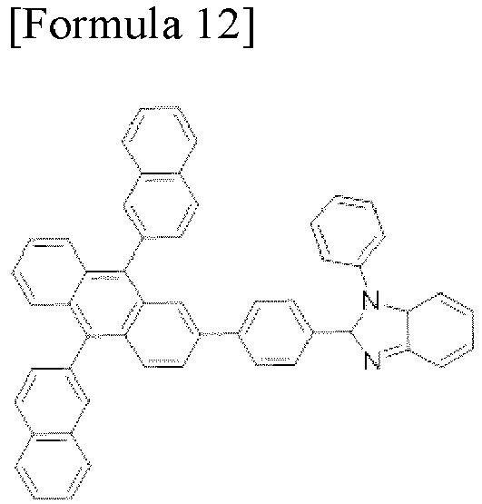
- The compound BH2-1 in Formula 4 was used as the host, and the compound BD2-1 in Formula 8 was used as the dopant.
- The compound BH2-1 in Formula 4 was used as the host, and the compound BD1-1 in Formula 7 was used as the dopant.
- On an anode (ITO, 1100Å), an HIL (the compound in Formula 9 and the compound in Formula 10 (20wt%), 100Å), an HTL (the compound in Formula 9, 800Å), an EBL (the compound in Formula 11, 150Å), a first blue emitting layer (a first host and a first dopant (1.5wt% doping), 50Å), a second blue emitting layer (a second host and a second dopant (2wt% doping), 200Å), an ETL (the compound in Formula 12, 200Å), an EII, (LiF, 15Å), and a cathode (Al, 1000Å) were sequentially stacked to form an OLED.
- The compound BH1-1 in Formula 2 was used as the first host, the compounds BD1-1, BD1-2 and BD1-3 in Formula 7 were used as the first dopant. The compound BH2-1 in in Formula 4 was used as the second host, and the compound BD1-1 in Formula 7 was used as the second dopant.
- The compound BH1-2 in Formula 2 was used as the first host, the compounds BD1-1, BD1-2 and BD1-3 in Formula 7 were used as the first dopant. The compound BH2-1 in in Formula 4 was used as the second host, and the compound BD1-1 in Formula 7 was used as the second dopant.
- The compound BH1-3 in Formula 2 was used as the first host, the compounds BD1-1, BD1-2 and BD1-3 in Formula 7 were used as the first dopant. The compound BH2-1 in in Formula 4 was used as the second host, and the compound BD1-1 in Formula 7 was used as the second dopant.
- The compound BH1-1 in Formula 2 was used as the first host, the compounds BD1-1, BD1-2 and BD1-3 in Formula 7 were used as the first dopant. The compound BH2-1 in in Formula 4 was used as the second host, and the compound BD2-1 in Formula 8 was used as the second dopant.
- The compound BH1-2 in Formula 2 was used as the first host, the compounds BD1-1, BD1-2 and BD1-3 in Formula 7 were used as the first dopant. The compound BH2-1 in in Formula 4 was used as the second host, and the compound BD2-1 in Formula 8 was used as the second dopant.
- The compound BH1-3 in Formula 2 was used as the first host, the compounds BD1-1, BD1-2 and BD1-3 in Formula 7 were used as the first dopant. The compound BH2-1 in in Formula 4 was used as the second host, and the compound BD2-1 in Formula 8 was used as the second dopant.
- The compound BH1-1 in Formula 2 was used as the first host, the compounds BD2-1, BD2-2 and BD2-3 in Formula 8 were used as the first dopant. The compound BH2-1 in in Formula 4 was used as the second host, and the compound BD1-1 in Formula 7 was used as the second dopant.
- The compound BH1-2 in Formula 2 was used as the first host, the compounds BD2-1, BD2-2 and BD2-3 in Formula 8 were used as the first dopant. The compound BH2-1 in in Formula 4 was used as the second host, and the compound BD1-1 in Formula 7 was used as the second dopant.
- The compound BH1-3 in Formula 2 was used as the first host, the compounds BD2-1, BD2-2 and BD2-3 in Formula 8 were used as the first dopant. The compound BH2-1 in in Formula 4 was used as the second host, and the compound BD1-1 in Formula 7 was used as the second dopant.
- The compound BH1-1 in Formula 2 was used as the first host, the compounds BD2-1, BD2-2 and BD2-3 in Formula 8 were used as the first dopant. The compound BH2-1 in in Formula 4 was used as the second host, and the compound BD2-1 in Formula 8 was used as the second dopant.
- The compound BH1-2 in Formula 2 was used as the first host, the compounds BD2-1, BD2-2 and BD2-3 in Formula 8 were used as the first dopant. The compound BH2-1 in in Formula 4 was used as the second host, and the compound BD2-1 in Formula 8 was used as the second dopant.
- The compound BH1-3 in Formula 2 was used as the first host, the compounds BD2-1, BD2-2 and BD2-3 in Formula 8 were used as the first dopant. The compound BH2-1 in in Formula 4 was used as the second host, and the compound BD2-1 in Formula 8 was used as the second dopant.
- The properties, i.e., a voltage (V), a color coordinate (CIEx, CIEy), an external quantum efficiency (EQE) and a lifespan (T95), of the OLEDs manufactured in Comparative Examples 1 and 2 and Examples 1 to 36 were measured and listed in Tables 1 to 4.
Table 1 B-EML Property (@10mA/cm2) T95 (%) B-EML1 B-EML2 Volt (V) Volt (V) @100J CIEx CIEy EQE (%) Ref1 BH2-1 + BD2-1 0 0 0.000 0.000 100.0% 100.0% Ref2 BH2-1 + BD1-1 -0.01 -0.02 -0.001 -0.005 90.5% 94.3% Ex1 BH1-1+BD1-1 BH2-1+BD1-1 -0.16 -0.12 -0.002 -0.003 95.3% 136.7% Ex2 BH1-1+BD1-2 BH2-1+BD1-1 -0.13 -0.10 -0.002 -0.004 96.5% 132.3% Ex3 BH1-1+BD1-3 BH2-1+BD1-1 -0.15 -0.12 -0.002 -0.003 95.0% 139.2% Ex4 BH1-2+BD1-1 BH2-1+BD1-1 -0.15 -0.11 -0.001 -0.002 94.7% 137.7% Ex5 BH1-2+BD1-2 BH2-1+BD1-1 -0.12 -0.08 -0.001 -0.003 95.6% 134.9% Ex6 BH1-2+BD1-3 BH2-1+BD1-1 -0.17 -0.13 -0.001 -0.003 94.8% 138.4% Ex7 BH1-3+BD1-1 BH2-1+BD1-1 -0.11 -0.07 -0.001 -0.003 95.2% 135.6% Ex8 BH1-3+BD1-2 BH2-1+BD1-1 -0.12 -0.08 -0.002 -0.004 96.7% 131.0% Ex9 BH1-3+BD1-3 BH2-1+BD1-1 -0.14 -0.09 -0.001 -0.003 94.9% 137.9% Table 2 B-EML Property (@10mA/cm2) T95 (%) B-EML1 B-EML2 Volt (V) Volt (V) @100J CIEx CIEy EQE (%) Ex10 BH1-1+BD1-1 BH2-1+BD2-1 -0.15 -0.10 -0.001 +0.001 102.0% 141.3% Ex11 BH1-1+BD1-2 BH2-1+BD2-1 -0.11 -0.05 -0.001 +0.000 102.6% 139.2% Ex12 BH1-1+BD1-3 BH2-1+BD2-1 -0.13 -0.07 -0.001 +0.001 101.7% 142.7% Ex13 BH1-2+BD1-1 BH2-1+BD2-1 -0.14 -0.09 -0.001 +0.001 101.5% 142.1% Ex14 BH1-2+BD1-2 BH2-1+BD2-1 -0.10 -0.05 -0.001 +0.001 101.8% 140.3% Ex15 BH1-2+BD1-3 BH2-1+BD2-1 -0.15 -0.10 -0.001 +0.001 101.6% 145.4% Ex16 BH1-3+BD1-1 BH2-1+BD2-1 -0.09 -0.04 -0.001 +0.001 102.1 % 139.1% Ex17 BH1-3+BD1-2 BH2-1+BD2-1 -0.11 -0.06 -0.001 +0.000 102.4% 138.3% Ex18 BH1-3+BD1-3 BH2-1+BD2-1 -0.12 -0.06 -0.001 +0.001 101.9% 140.3% Table 3 B-EML Property (@10mA/cm2) T95 (%) B-EML1 B-EML2 Volt (V) Volt (V) @100J CIEx CIEy EQE (%) Ex19 BH1-1+BD2-1 BH2-1+BD1-1 -0.16 -0.11 -0.002 -0.001 97.0% 139.6% Ex20 BH1-1+BD2-2 BH2-1+BD1-1 -0.14 -0.09 -0.002 -0.001 96.4% 138.7% Ex21 BH1-1+BD2-3 BH2-1+BD1-1 -0.13 -0.09 -0.002 -0.002 98.0% 137.3% Ex22 BH1-2+BD2-1 BH2-1+BD1-1 -0.15 -0.11 -0.002 -0.001 96.6% 141.6% Ex23 BH1-2+BD2-2 BH2-1+BD1-1 -0.11 -0.05 -0.002 -0.001 97.0% 140.9% Ex24 BH1-2+BD2-3 BH2-1+BD1-1 -0.16 -0.10 -0.002 -0.002 97.6% 140.1% Ex25 BH1-3+BD2-1 BH2-1+BD1-1 -0.08 -0.03 -0.002 -0.001 97.2% 138.9% Ex26 BH1-3+BD2-2 BH2-1+BD1-1 -0.08 -0.04 -0.002 -0.001 96.7% 139.2% Ex27 BH1-3+BD2-3 BH2-1+BD1-1 -0.10 -0.04 -0.002 -0.002 97.8% 138.4% Table 4 B-EML Property (@10mA/cm2) T95 (%) B-EML1 B-EML2 Volt (V) Volt (V) @100J CIEx ClEy EQE (%) Ex28 BH1-1+BD2-1 BH2-1+BD2-1 -0.17 -0.12 -0.001 +0.004 103.6% 145.0% Ex29 BH1-1+B02-2 BH2-1+BD2-1 -0.15 -0.10 -0.001 +0.004 103.0% 144.4% Ex30 BH1-1+BD2-3 BH2-1+BD2-1 -0.15 -0.08 -0.001 +0.003 104.1 % 144.0% Ex31 BH1-2+BD2-1 BH2-1+BD2-1 -0.14 -0.09 -0.001 +0.004 103.2% 146.4% Ex32 BH1-2+BD2-2 BH2-1+BD2-1 -0.10 -0.06 -0.001 +0.003 103.3% 145.9% Ex33 BH1-2+BD2-3 BH2-1+BD2-1 -0.17 -0.12 -0.001 +0.003 103.9% 144.7% Ex34 BH1-3+BD2-1 BH2-1+BD2-1 -0.09 -0.04 -0.001 +0.004 103.0% 145.4% Ex35 BH1-3+BD2-2 BH2-1+BD2-1 -0.11 -0.08 -0.001 +0.004 102.8% 144.9% Ex36 BH1-3+BD2-3 BH2-1+BD2-1 -0.13 -0.10 -0.001 +0.003 103.7% 144.7% - As shown in Tables 1 to 4, in comparison to the OLED of Comparative Examples 1 and 2, the OLED of Examples 1 to 36 has an advantage in at least one of the driving voltage, the color purity, the emitting efficiency and the lifespan.
- In addition, as shown in Examples 10 to 18, when the first dopant in the first blue emitting layer is the compound represented by Formula 5 and the second dopant in the second blue emitting layer is the compound represented by Formula 6, the OLED has big advantage in the driving voltage, the emitting efficiency and the lifespan with sufficient color purity.
- As shown in Examples 19 to 27, when the first dopant in the first blue emitting layer is the compound represented by Formula 6 and the second dopant in the second blue emitting layer is the compound represented by Formula 5, the OLED has big advantage in the driving voltage, the color purity and the lifespan with sufficient emitting efficiency.
- As shown in Examples 28 to 36, when the first dopant in the first blue emitting layer is the compound represented by Formula 6 and the second dopant in the second blue emitting layer is the compound represented by Formula 6, the OLED has big advantage in the driving voltage, the color purity and the lifespan with sufficient emitting efficiency.
- On an anode (ITO, 1100Å), an HIL (the compound in Formula 9 and the compound in Formula 10 (20wt%), 100Å), an HTL (the compound in Formula 9, 800Å), an EBL (the compound in Formula 11, 150Å), a first blue emitting layer (a first host and a first dopant (the compound BD2-1 in Formula 8, 1.5wt% doping)), a second blue emitting layer (a second host and a second dopant (the compound BD2-1 in Formula 8, 1.5wt% doping)), an ETL (the compound in Formula 12, 200Å), an EII, (LiF, 15Å), and a cathode (Al, 1000Å) were sequentially stacked to form an OLED.
- The compound BH1-1 in Formula 2 was used as the first host to form the first blue emitting layer (25 Å), and the compound BH2-1 in Formula 4 was used as the second host to form the second blue emitting layer (225 Å).
- The compound BH1-1 in Formula 2 was used as the first host to form the first blue emitting layer (50 Å), and the compound BH2-1 in Formula 4 was used as the second host to form the second blue emitting layer (200 Å).
- The compound BH1-1 in Formula 2 was used as the first host to form the first blue emitting layer (75 Å), and the compound BH2-1 in Formula 4 was used as the second host to form the second blue emitting layer (175 Å).
- The compound BH1-2 in Formula 2 was used as the first host to form the first blue emitting layer (25 Å), and the compound BH2-1 in Formula 4 was used as the second host to form the second blue emitting layer (225 Å).
- The compound BH1-2 in Formula 2 was used as the first host to form the first blue emitting layer (50 Å), and the compound BH2-1 in Formula 4 was used as the second host to form the second blue emitting layer (200 Å).
- The compound BH1-2 in Formula 2 was used as the first host to form the first blue emitting layer (75 Å), and the compound BH2-1 in Formula 4 was used as the second host to form the second blue emitting layer (175 Å).
- The properties, i.e., a voltage (V), a color coordinate (CIEx, CIEy), an external quantum efficiency (EQE) and a lifespan (T95), of the OLEDs manufactured in Comparative Example 1 and Examples 37 to 42 were measured and listed in Table 5.
Table 5 B-EML Property (@10mA/cm2) T95 (%) B-EML1 B-EML2 Volt (V) Volt (V) @100J CIEx CIEy EQE (%) Ref1 BH2-1 (250Å) 0 0 0.000 0.000 100.0% 100.0% Ex37 BH1-1 (25Å) BH2-1 (225Å) -0.02 -0.03 -0.002 +0.004 103% 141% Ex38 BH1-1 (50Å) BH2-1 (200Å) -0.06 -0.11 -0.002 +0.005 104% 145% Ex39 BH1-1 (75Å) BH2-1 (175Å) -0.05 -0.11 -0.002 +0.006 103% 135% Ex40 BH1-2 (25Å) BH2-1 (225Å) -0.01 -0.01 -0.001 +0.004 102.7% 145.7% Ex41 BH1-2 (50Å) BH2-1 (200Å) -0.03 -0.05 -0.001 +0.004 103.2% 146.4% Ex42 BH1-2 (75Å) BH2-1 (175Å) -0.04 -0.05 -0.001 +0.005 103.0% 146.0% - As shown in Table 5, when a thickness of the first blue emitting layer, which includes the first host represented by
Formula 1, is smaller than that of the second blue emitting layer, which includes the second host represented byFormula 3, the OLED has an advantage in at least one of the driving voltage, the color purity, the emitting efficiency and the lifespan. - In addition, as the OLEDs in Examples 38 and 41, when a thickness, e.g., 50Å, of the first blue emitting layer is about 1/4 of a thickness, e.g., 200Å, of the second blue emitting layer, the OLED has big advantage in at least one of the driving voltage, the color purity, the emitting efficiency and the lifespan.
- It will be apparent to those skilled in the art that various modifications and variations can be made in the embodiments of the present invention without departing from the spirit or scope of the present invention. Thus, it is intended that the modifications and variations cover this invention provided they come within the scope of the appended claims and their equivalents.

each of f1 and f2 is independently an integer of 0 to 4, f3 is an integer of 0 to 3, f4 is 0 or 1, X is O or S, each of Ar31 and Ar32 is independently selected from the group consisting of a substituted or unsubstituted C6 to C30 arylamino group, a substituted or unsubstituted C6 to C30 aryl group, a substituted or unsubstituted C3 to C30 heteroaryl group and a substituted or unsubstituted C6 to C30 alicyclic group or forms a substituted or unsubstituted ring with adjacent benzene ring, and each of R31, R32 and R33 is independently selected from the group consisting of a substituted or unsubstituted C1 to C30 alkyl group, a substituted or unsubstituted C3 to C30 cycloalkyl group, a substituted or unsubstituted C6 to C30 arylamino group, a substituted or unsubstituted C6 to C30 aryl group and a substituted or unsubstituted C3 to C30 heteroaryl group.
In an embodiment, wherein the first dopant is represented by one of the Formulas 5 and 6, and the second dopant is represented by the other one of the Formulas 5 and 6.


In an embodiment, the organic light emitting diode further comprises:
a second emitting part including a third blue emitting layer and a fourth blue emitting layer and positioned between the first emitting part and the second electrode, the fourth blue emitting layer positioned between the third blue emitting layer and the second electrode and contacting the third blue emitting layer,

In an embodiment, the organic light emitting diode further comprises:
a third emitting part including a red emitting layer and a green emitting layer and positioned between the first and second emitting parts.
In an embodiment, the organic light emitting diode further comprises:
a second emitting part including a yellow-green emitting layer and positioned between the first emitting part and the second electrode.
Claims (15)
- An organic light emitting diode, comprising:a first electrode;a second electrode facing the first electrode; anda first emitting part including a first blue emitting layer and a second blue emitting layer and positioned between the first and second electrodes, the second blue emitting layer positioned between the first blue emitting layer and the second electrode and contacting the first blue emitting layer,wherein the first blue emitting layer includes a first host and a first dopant, and the second blue emitting layer includes a second host and a second dopant,wherein the first host is a pyrene derivative, and the second host is an anthracene derivative,wherein the first dopant is a first compound represented by Formula 5 or a second compound represented by Formula 6, and the second dopant is a third compound represented by Formula 5 or a fourth compound represented by Formula 6,
 each of e1 and e2 is independently an integer of 0 to 4, and e3 is an integer of 0 to 3,each of Ar21 and Ar22 is independently selected from the group consisting of a substituted or unsubstituted C6 to C30 arylamino group, a substituted or unsubstituted C6 to C30 aryl group, a substituted or unsubstituted C3 to C30 heteroaryl group and a substituted or unsubstituted C6 to C30 alicyclic group, andR21, R22 and R23 is independently selected from the group consisting of a substituted or unsubstituted C1 to C30 alkyl group, a substituted or unsubstituted C3 to C30 cycloalkyl group, a substituted or unsubstituted C6 to C30 arylamino group, a substituted or unsubstituted C6 to C30 aryl group and a substituted or unsubstituted C3 to C30 heteroaryl group,
 each of f1 and f2 is independently an integer of 0 to 4, f3 is an integer of 0 to 3, f4 is 0 or 1,X is O or S,each of Ar31 and Ar32 is independently selected from the group consisting of a substituted or unsubstituted C6 to C30 arylamino group, a substituted or unsubstituted C6 to C30 aryl group, a substituted or unsubstituted C3 to C30 heteroaryl group and a substituted or unsubstituted C6 to C30 alicyclic group or forms a substituted or unsubstituted ring with adjacent benzene ring, andeach of R31, R32 and R33 is independently selected from the group consisting of a substituted or unsubstituted C1 to C30 alkyl group, a substituted or unsubstituted C3 to C30 cycloalkyl group, a substituted or unsubstituted C6 to C30 arylamino group, a substituted or unsubstituted C6 to C30 aryl group and a substituted or unsubstituted C3 to C30 heteroaryl group.
 - The organic light emitting diode according to claim 1, wherein the first dopant is represented by one of the Formulas 5 and 6, and the second dopant is represented by the other one of the Formulas 5 and 6.
- The organic light emitting diode according to any of claims 1 to 2, wherein when the first dopant is the first compound and the second dopant is the fourth compound, a weight % of the first dopant in the first blue emitting material layer is smaller than a weight % of the second dopant in the second blue emitting material layer, or
wherein when the first dopant is the second compound and the second dopant is the third compound, a weight % of the first dopant in the first blue emitting material layer is greater than a weight % of the second dopant in the second blue emitting material layer. - The organic light emitting diode according to any of claims 1 to 3, wherein each of the first compound and the third compound is independently one of compounds in Formula 7:
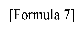

- The organic light emitting diode according to any of claims 1 to 4, wherein each of the second compound and the fourth compound is independently one of compounds in Formula 8:
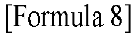

- The organic light emitting diode according to any of claims 1 to 5, wherein the first host is represented by Formula 1:
 each of a1 and a2 is independently 0 or 1, and a3 is an integer of 0 to 4,R1 is selected from the group consisting of deuterium, a substituted or unsubstituted C1 to C30 alkyl group, a substituted or unsubstituted C1 to C30 alkoxy group, a substituted or unsubstituted C6 to C30 aryl group and a substituted or unsubstituted C3 to C30 heteroaryl group,each of Ar1 and Ar2 is independently selected from the group consisting of hydrogen, deuterium, a substituted or unsubstituted C6 to C30 aryl group and a substituted or unsubstituted C3 to C30 heteroaryl group, andeach of L1 and L2 is independently selected from the group consisting of a substituted or unsubstituted C6 to C30 arylene group and a substituted or unsubstituted C3 to C30 heteroarylene group.
 - The organic light emitting diode according to any of claims 1 to 6, wherein the first host includes at least one of first host compounds in Formula 2:


- The organic light emitting diode according to any of claims 1 to 7, wherein the second host is represented by Formula 3:
 each of b1 and b2 is independently 0 or 1, and b3 is an integer of 0 to 8,R11 is selected from the group consisting of deuterium, a substituted or unsubstituted C1 to C30 alkyl group, a substituted or unsubstituted C1 to C30 alkoxy group, a substituted or unsubstituted C6 to C30 aryl group and a substituted or unsubstituted C3 to C30 heteroaryl group,each of L11 and L12 is independently selected from the group consisting of a substituted or unsubstituted C6 to C30 arylene group and a substituted or unsubstituted C3 to C30 heteroarylene group, andeach of Ar11 and Ar12 is independently selected from the group consisting of a substituted or unsubstituted C6 to C30 aryl group and a substituted or unsubstituted C3 to C30 heteroaryl group.
 - The organic light emitting diode according to any of claims 1 to 8, wherein the second host includes at least one of second host compounds in Formula 4:


- The organic light emitting diode according to any of claims 1 to 9, further comprising:a second emitting part including a third blue emitting layer and a fourth blue emitting layer and positioned between the first emitting part and the second electrode, the fourth blue emitting layer positioned between the third blue emitting layer and the second electrode and contacting the third blue emitting layer,wherein the third blue emitting layer includes a third host and a third dopant, and the fourth blue emitting layer includes a fourth host and a fourth dopant,wherein the third host is the pyrene derivative, and the fourth host is the anthracene derivative,wherein the third dopant is a fifth compound represented by the Formula 5 or a sixth compound represented by the Formula 6, and the second dopant is a seventh compound represented by the Formula 5 or an eighth compound represented by the Formula 6.
- The organic light emitting diode according to claim 10, wherein the third dopant is represented by one of the Formulas 5 and 6, and the fourth dopant is represented by the other one of the Formulas 5 and 6.
- The organic light emitting diode according to any of claims 10 to 11, wherein wherein when the third dopant is the fifth compound and the fourth dopant is the eighth compound, a weight % of the third dopant in the third blue emitting material layer is smaller than a weight % of the fourth dopant in the fourth blue emitting material layer, or
wherein when the third dopant is the sixth compound and the second dopant is the seventh compound, a weight % of the third dopant in the third blue emitting material layer is greater than a weight % of the fourth dopant in the fourth blue emitting material layer. - The organic light emitting diode according to any of claims 10 to 12, wherein the third host is represented by Formula 1:

 each of a1 and a2 is independently 0 or 1, and a3 is an integer of 0 to 4,R1 is selected from the group consisting of deuterium, a substituted or unsubstituted C1 to C30 alkyl group, a substituted or unsubstituted C1 to C30 alkoxy group, a substituted or unsubstituted C6 to C30 aryl group and a substituted or unsubstituted C3 to C30 heteroaryl group,each of Ar1 and Ar2 is independently selected from the group consisting of hydrogen, deuterium, a substituted or unsubstituted C6 to C30 aryl group and a substituted or unsubstituted C3 to C30 heteroaryl group, andeach of L1 and L2 is independently selected from the group consisting of a substituted or unsubstituted C6 to C30 arylene group and a substituted or unsubstituted C3 to C30 heteroarylene group.
 - The organic light emitting diode according to any of claims 10 to 13, wherein the fourth host is represented by Formula 3:

 each of b1 and b2 is independently 0 or 1, and b3 is an integer of 0 to 8,R11 is selected from the group consisting of deuterium, a substituted or unsubstituted C1 to C30 alkyl group, a substituted or unsubstituted C1 to C30 alkoxy group, a substituted or unsubstituted C6 to C30 aryl group and a substituted or unsubstituted C3 to C30 heteroaryl group,each of L11 and L12 is independently selected from the group consisting of a substituted or unsubstituted C6 to C30 arylene group and a substituted or unsubstituted C3 to C30 heteroarylene group, andeach of Ar11 and Ar12 is independently selected from the group consisting of a substituted or unsubstituted C6 to C30 aryl group and a substituted or unsubstituted C3 to C30 heteroaryl group.
 - An organic light emitting device, comprising:a substrate;an organic light emitting diode of any of claims 1 to 14 over the substrate; andan encapsulation layer covering the organic light emitting diode.
Applications Claiming Priority (1)
| Application Number | Priority Date | Filing Date | Title |
|---|---|---|---|
| KR20220189154 | 2022-12-29 |
Publications (2)
| Publication Number | Publication Date |
|---|---|
| EP4395515A1 true EP4395515A1 (en) | 2024-07-03 |
| EP4395515B1 EP4395515B1 (en) | 2026-02-18 |
Family
ID=87863459
Family Applications (1)
| Application Number | Title | Priority Date | Filing Date |
|---|---|---|---|
| EP23194259.0A Active EP4395515B1 (en) | 2022-12-29 | 2023-08-30 | Organic light emitting diode and organic light emitting device including the same |
Country Status (4)
| Country | Link |
|---|---|
| US (1) | US20240244969A1 (en) |
| EP (1) | EP4395515B1 (en) |
| KR (1) | KR20240106941A (en) |
| CN (1) | CN118284281A (en) |
Families Citing this family (1)
| Publication number | Priority date | Publication date | Assignee | Title |
|---|---|---|---|---|
| CN121895956B (en) * | 2026-03-20 | 2026-05-29 | 石家庄诚志永华显示材料有限公司 | Organic composition for double-luminescent-layer blue light device and double-luminescent-layer blue light organic electroluminescent device comprising same |
Citations (5)
| Publication number | Priority date | Publication date | Assignee | Title |
|---|---|---|---|---|
| JP2007294261A (en) * | 2006-04-25 | 2007-11-08 | Matsushita Electric Works Ltd | Organic electroluminescence device |
| US20110251446A1 (en) * | 2008-12-19 | 2011-10-13 | Canon Kabushiki Kaisha | DIACENAPHTHO[1,2-b:1',2'-k]CHRYSENE DERIVATIVE |
| WO2021010656A1 (en) * | 2019-07-18 | 2021-01-21 | 주식회사 엘지화학 | Organic light emitting element |
| US20220209119A1 (en) * | 2020-12-28 | 2022-06-30 | Lg Display Co., Ltd. | Organic light emitting device |
| US20220285625A1 (en) * | 2018-10-16 | 2022-09-08 | Idemitsu Kosan Co.,Ltd. | Organic electroluminescence device and electronic apparatus |
-
2023
- 2023-08-08 US US18/231,450 patent/US20240244969A1/en active Pending
- 2023-08-22 CN CN202311058297.2A patent/CN118284281A/en active Pending
- 2023-08-30 EP EP23194259.0A patent/EP4395515B1/en active Active
- 2023-09-08 KR KR1020230119779A patent/KR20240106941A/en active Pending
Patent Citations (5)
| Publication number | Priority date | Publication date | Assignee | Title |
|---|---|---|---|---|
| JP2007294261A (en) * | 2006-04-25 | 2007-11-08 | Matsushita Electric Works Ltd | Organic electroluminescence device |
| US20110251446A1 (en) * | 2008-12-19 | 2011-10-13 | Canon Kabushiki Kaisha | DIACENAPHTHO[1,2-b:1',2'-k]CHRYSENE DERIVATIVE |
| US20220285625A1 (en) * | 2018-10-16 | 2022-09-08 | Idemitsu Kosan Co.,Ltd. | Organic electroluminescence device and electronic apparatus |
| WO2021010656A1 (en) * | 2019-07-18 | 2021-01-21 | 주식회사 엘지화학 | Organic light emitting element |
| US20220209119A1 (en) * | 2020-12-28 | 2022-06-30 | Lg Display Co., Ltd. | Organic light emitting device |
Also Published As
| Publication number | Publication date |
|---|---|
| CN118284281A (en) | 2024-07-02 |
| EP4395515B1 (en) | 2026-02-18 |
| KR20240106941A (en) | 2024-07-08 |
| US20240244969A1 (en) | 2024-07-18 |
Similar Documents
| Publication | Publication Date | Title |
|---|---|---|
| EP4038667B1 (en) | Organic light emitting diode and organic light emitting device having the same | |
| KR20220093837A (en) | Organic light emitting device | |
| EP4395515B1 (en) | Organic light emitting diode and organic light emitting device including the same | |
| US20240244857A1 (en) | Organic compound, organic light emitting diode and organic light emitting device having the compound | |
| US12575322B2 (en) | Organic light emitting diode and organic light emitting display device including the same | |
| EP4199686A1 (en) | Organic light emitting diode and organic light emitting device including the same | |
| EP4395516B1 (en) | Organic light emitting diode and organic light emitting device including the same | |
| EP4395517B1 (en) | Organic light emitting diode and organic light emitting device including the same | |
| EP4395518B1 (en) | Organic light emitting diode and organic light emitting device including the same | |
| KR20240059262A (en) | Organic light emitting diode and organic light emitting device including the same | |
| US20240244871A1 (en) | Organic light emitting diode and organic light emitting device including the same | |
| US20250275475A1 (en) | Organic light emitting diode and organic light emitting device including the same | |
| US20240276751A1 (en) | Organic light emitting device | |
| US20240237377A1 (en) | Organic light emitting diode and organic light emitting display device including the same | |
| US20250241118A1 (en) | Organic light emitting diode and organic light emitting device including the same | |
| US20240244967A1 (en) | Organic Light Emitting Diode and Organic Light Emitting Device Including the Same | |
| US20240179932A1 (en) | Organic light emitting diode and organic light emitting device including the same | |
| US20240246997A1 (en) | Organic compound, organic light emitting diode and organic light emitting device including the same | |
| EP4203645A2 (en) | Organic light emitting diode and organic light emitting display device including the same | |
| US20240237525A1 (en) | Organic Light Emitting Diode and Organic Light Emitting Device Including the Same | |
| KR20250131874A (en) | Organic light emitting diode and organic light emitting device including the same | |
| KR20250131297A (en) | Organic compound and organic light emitting diode and organic light emitting device including the same |
Legal Events
| Date | Code | Title | Description |
|---|---|---|---|
| PUAI | Public reference made under article 153(3) epc to a published international application that has entered the european phase |
Free format text: ORIGINAL CODE: 0009012 |
|
| STAA | Information on the status of an ep patent application or granted ep patent |
Free format text: STATUS: REQUEST FOR EXAMINATION WAS MADE |
|
| 17P | Request for examination filed |
Effective date: 20230830 |
|
| AK | Designated contracting states |
Kind code of ref document: A1 Designated state(s): AL AT BE BG CH CY CZ DE DK EE ES FI FR GB GR HR HU IE IS IT LI LT LU LV MC ME MK MT NL NO PL PT RO RS SE SI SK SM TR |
|
| RBV | Designated contracting states (corrected) |
Designated state(s): AL AT BE BG CH CY CZ DE DK EE ES FI FR GB GR HR HU IE IS IT LI LT LU LV MC ME MK MT NL NO PL PT RO RS SE SI SK SM TR |
|
| STAA | Information on the status of an ep patent application or granted ep patent |
Free format text: STATUS: EXAMINATION IS IN PROGRESS |
|
| 17Q | First examination report despatched |
Effective date: 20241205 |
|
| GRAP | Despatch of communication of intention to grant a patent |
Free format text: ORIGINAL CODE: EPIDOSNIGR1 |
|
| STAA | Information on the status of an ep patent application or granted ep patent |
Free format text: STATUS: GRANT OF PATENT IS INTENDED |
|
| INTG | Intention to grant announced |
Effective date: 20250915 |
|
| GRAS | Grant fee paid |
Free format text: ORIGINAL CODE: EPIDOSNIGR3 |
|
| GRAA | (expected) grant |
Free format text: ORIGINAL CODE: 0009210 |
|
| STAA | Information on the status of an ep patent application or granted ep patent |
Free format text: STATUS: THE PATENT HAS BEEN GRANTED |
|
| AK | Designated contracting states |
Kind code of ref document: B1 Designated state(s): AL AT BE BG CH CY CZ DE DK EE ES FI FR GB GR HR HU IE IS IT LI LT LU LV MC ME MK MT NL NO PL PT RO RS SE SI SK SM TR |
|
| REG | Reference to a national code |
Ref country code: CH Ref legal event code: F10 Free format text: ST27 STATUS EVENT CODE: U-0-0-F10-F00 (AS PROVIDED BY THE NATIONAL OFFICE) Effective date: 20260218 Ref country code: GB Ref legal event code: FG4D |
|
| REG | Reference to a national code |
Ref country code: IE Ref legal event code: FG4D |
|
| REG | Reference to a national code |
Ref country code: DE Ref legal event code: R096 Ref document number: 602023012121 Country of ref document: DE |
|
| REG | Reference to a national code |
Ref country code: NL Ref legal event code: MP Effective date: 20260218 |
|
| PG25 | Lapsed in a contracting state [announced via postgrant information from national office to epo] |
Ref country code: RS Free format text: LAPSE BECAUSE OF FAILURE TO SUBMIT A TRANSLATION OF THE DESCRIPTION OR TO PAY THE FEE WITHIN THE PRESCRIBED TIME-LIMIT Effective date: 20260518 |
|
| PG25 | Lapsed in a contracting state [announced via postgrant information from national office to epo] |
Ref country code: ES Free format text: LAPSE BECAUSE OF FAILURE TO SUBMIT A TRANSLATION OF THE DESCRIPTION OR TO PAY THE FEE WITHIN THE PRESCRIBED TIME-LIMIT Effective date: 20260218 |
|
| PG25 | Lapsed in a contracting state [announced via postgrant information from national office to epo] |
Ref country code: PL Free format text: LAPSE BECAUSE OF FAILURE TO SUBMIT A TRANSLATION OF THE DESCRIPTION OR TO PAY THE FEE WITHIN THE PRESCRIBED TIME-LIMIT Effective date: 20260218 |
|
| PG25 | Lapsed in a contracting state [announced via postgrant information from national office to epo] |
Ref country code: GR Free format text: LAPSE BECAUSE OF FAILURE TO SUBMIT A TRANSLATION OF THE DESCRIPTION OR TO PAY THE FEE WITHIN THE PRESCRIBED TIME-LIMIT Effective date: 20260519 |
|
| REG | Reference to a national code |
Ref country code: LT Ref legal event code: MG9D |
|
| PG25 | Lapsed in a contracting state [announced via postgrant information from national office to epo] |
Ref country code: LT Free format text: LAPSE BECAUSE OF FAILURE TO SUBMIT A TRANSLATION OF THE DESCRIPTION OR TO PAY THE FEE WITHIN THE PRESCRIBED TIME-LIMIT Effective date: 20260218 |
|
| PG25 | Lapsed in a contracting state [announced via postgrant information from national office to epo] |
Ref country code: NO Free format text: LAPSE BECAUSE OF FAILURE TO SUBMIT A TRANSLATION OF THE DESCRIPTION OR TO PAY THE FEE WITHIN THE PRESCRIBED TIME-LIMIT Effective date: 20260518 |
|
| PG25 | Lapsed in a contracting state [announced via postgrant information from national office to epo] |
Ref country code: SE Free format text: LAPSE BECAUSE OF FAILURE TO SUBMIT A TRANSLATION OF THE DESCRIPTION OR TO PAY THE FEE WITHIN THE PRESCRIBED TIME-LIMIT Effective date: 20260218 Ref country code: FI Free format text: LAPSE BECAUSE OF FAILURE TO SUBMIT A TRANSLATION OF THE DESCRIPTION OR TO PAY THE FEE WITHIN THE PRESCRIBED TIME-LIMIT Effective date: 20260218 Ref country code: AT Free format text: LAPSE BECAUSE OF FAILURE TO SUBMIT A TRANSLATION OF THE DESCRIPTION OR TO PAY THE FEE WITHIN THE PRESCRIBED TIME-LIMIT Effective date: 20260218 |
|
| REG | Reference to a national code |
Ref country code: AT Ref legal event code: MK05 Ref document number: 1889695 Country of ref document: AT Kind code of ref document: T Effective date: 20260218 |
|
| PG25 | Lapsed in a contracting state [announced via postgrant information from national office to epo] |
Ref country code: HR Free format text: LAPSE BECAUSE OF FAILURE TO SUBMIT A TRANSLATION OF THE DESCRIPTION OR TO PAY THE FEE WITHIN THE PRESCRIBED TIME-LIMIT Effective date: 20260218 |
|
| PG25 | Lapsed in a contracting state [announced via postgrant information from national office to epo] |
Ref country code: PT Free format text: LAPSE BECAUSE OF FAILURE TO SUBMIT A TRANSLATION OF THE DESCRIPTION OR TO PAY THE FEE WITHIN THE PRESCRIBED TIME-LIMIT Effective date: 20260618 Ref country code: IS Free format text: LAPSE BECAUSE OF FAILURE TO SUBMIT A TRANSLATION OF THE DESCRIPTION OR TO PAY THE FEE WITHIN THE PRESCRIBED TIME-LIMIT Effective date: 20260618 |
|
| PG25 | Lapsed in a contracting state [announced via postgrant information from national office to epo] |
Ref country code: NL Free format text: LAPSE BECAUSE OF FAILURE TO SUBMIT A TRANSLATION OF THE DESCRIPTION OR TO PAY THE FEE WITHIN THE PRESCRIBED TIME-LIMIT Effective date: 20260218 |
|
| PG25 | Lapsed in a contracting state [announced via postgrant information from national office to epo] |
Ref country code: LV Free format text: LAPSE BECAUSE OF FAILURE TO SUBMIT A TRANSLATION OF THE DESCRIPTION OR TO PAY THE FEE WITHIN THE PRESCRIBED TIME-LIMIT Effective date: 20260218 |
|
| PG25 | Lapsed in a contracting state [announced via postgrant information from national office to epo] |
Ref country code: BG Free format text: LAPSE BECAUSE OF FAILURE TO SUBMIT A TRANSLATION OF THE DESCRIPTION OR TO PAY THE FEE WITHIN THE PRESCRIBED TIME-LIMIT Effective date: 20260218 |