EP4395157A1 - Primary variable speed generator-motor device - Google Patents
Primary variable speed generator-motor device Download PDFInfo
- Publication number
- EP4395157A1 EP4395157A1 EP21954952.4A EP21954952A EP4395157A1 EP 4395157 A1 EP4395157 A1 EP 4395157A1 EP 21954952 A EP21954952 A EP 21954952A EP 4395157 A1 EP4395157 A1 EP 4395157A1
- Authority
- EP
- European Patent Office
- Prior art keywords
- level
- phase
- command
- current
- signal
- Prior art date
- Legal status (The legal status is an assumption and is not a legal conclusion. Google has not performed a legal analysis and makes no representation as to the accuracy of the status listed.)
- Pending
Links
Images















Classifications
-
- H—ELECTRICITY
- H02—GENERATION; CONVERSION OR DISTRIBUTION OF ELECTRIC POWER
- H02P—CONTROL OR REGULATION OF ELECTRIC MOTORS, ELECTRIC GENERATORS OR DYNAMO-ELECTRIC CONVERTERS; CONTROLLING TRANSFORMERS, REACTORS OR CHOKE COILS
- H02P9/00—Arrangements for controlling electric generators for the purpose of obtaining a desired output
- H02P9/10—Control effected upon generator excitation circuit to reduce harmful effects of overloads or transients, e.g. sudden application of load, sudden removal of load, sudden change of load
-
- H—ELECTRICITY
- H02—GENERATION; CONVERSION OR DISTRIBUTION OF ELECTRIC POWER
- H02P—CONTROL OR REGULATION OF ELECTRIC MOTORS, ELECTRIC GENERATORS OR DYNAMO-ELECTRIC CONVERTERS; CONTROLLING TRANSFORMERS, REACTORS OR CHOKE COILS
- H02P21/00—Arrangements or methods for the control of electric machines by vector control, e.g. by control of field orientation
- H02P21/22—Current control, e.g. using a current control loop
-
- H—ELECTRICITY
- H02—GENERATION; CONVERSION OR DISTRIBUTION OF ELECTRIC POWER
- H02M—APPARATUS FOR CONVERSION BETWEEN AC AND AC, BETWEEN AC AND DC, OR BETWEEN DC AND DC, AND FOR USE WITH MAINS OR SIMILAR POWER SUPPLY SYSTEMS; CONVERSION OF DC OR AC INPUT POWER INTO SURGE OUTPUT POWER; CONTROL OR REGULATION THEREOF
- H02M1/00—Details of apparatus for conversion
- H02M1/32—Means for protecting converters other than automatic disconnection
-
- H—ELECTRICITY
- H02—GENERATION; CONVERSION OR DISTRIBUTION OF ELECTRIC POWER
- H02M—APPARATUS FOR CONVERSION BETWEEN AC AND AC, BETWEEN AC AND DC, OR BETWEEN DC AND DC, AND FOR USE WITH MAINS OR SIMILAR POWER SUPPLY SYSTEMS; CONVERSION OF DC OR AC INPUT POWER INTO SURGE OUTPUT POWER; CONTROL OR REGULATION THEREOF
- H02M7/00—Conversion of AC power input into DC power output; Conversion of DC power input into AC power output
- H02M7/42—Conversion of DC power input into AC power output without possibility of reversal
- H02M7/44—Conversion of DC power input into AC power output without possibility of reversal by static converters
- H02M7/48—Conversion of DC power input into AC power output without possibility of reversal by static converters using discharge tubes with control electrode or semiconductor devices with control electrode
- H02M7/483—Converters with outputs that each can have more than two voltages levels
- H02M7/487—Neutral point clamped inverters
-
- H—ELECTRICITY
- H02—GENERATION; CONVERSION OR DISTRIBUTION OF ELECTRIC POWER
- H02P—CONTROL OR REGULATION OF ELECTRIC MOTORS, ELECTRIC GENERATORS OR DYNAMO-ELECTRIC CONVERTERS; CONTROLLING TRANSFORMERS, REACTORS OR CHOKE COILS
- H02P27/00—Arrangements or methods for the control of AC motors characterised by the kind of supply voltage
- H02P27/04—Arrangements or methods for the control of AC motors characterised by the kind of supply voltage using variable-frequency supply voltage, e.g. inverter or converter supply voltage
- H02P27/06—Arrangements or methods for the control of AC motors characterised by the kind of supply voltage using variable-frequency supply voltage, e.g. inverter or converter supply voltage using DC to AC converters or inverters
- H02P27/08—Arrangements or methods for the control of AC motors characterised by the kind of supply voltage using variable-frequency supply voltage, e.g. inverter or converter supply voltage using DC to AC converters or inverters with pulse width modulation
- H02P27/14—Arrangements or methods for the control of AC motors characterised by the kind of supply voltage using variable-frequency supply voltage, e.g. inverter or converter supply voltage using DC to AC converters or inverters with pulse width modulation with three or more levels of voltage
-
- H—ELECTRICITY
- H02—GENERATION; CONVERSION OR DISTRIBUTION OF ELECTRIC POWER
- H02P—CONTROL OR REGULATION OF ELECTRIC MOTORS, ELECTRIC GENERATORS OR DYNAMO-ELECTRIC CONVERTERS; CONTROLLING TRANSFORMERS, REACTORS OR CHOKE COILS
- H02P29/00—Arrangements for regulating or controlling electric motors, appropriate for both AC and DC motors
- H02P29/02—Providing protection against overload without automatic interruption of supply
- H02P29/024—Detecting a fault condition, e.g. short circuit, locked rotor, open circuit or loss of load
- H02P29/028—Detecting a fault condition, e.g. short circuit, locked rotor, open circuit or loss of load the motor continuing operation despite the fault condition, e.g. eliminating, compensating for or remedying the fault
-
- H—ELECTRICITY
- H02—GENERATION; CONVERSION OR DISTRIBUTION OF ELECTRIC POWER
- H02M—APPARATUS FOR CONVERSION BETWEEN AC AND AC, BETWEEN AC AND DC, OR BETWEEN DC AND DC, AND FOR USE WITH MAINS OR SIMILAR POWER SUPPLY SYSTEMS; CONVERSION OF DC OR AC INPUT POWER INTO SURGE OUTPUT POWER; CONTROL OR REGULATION THEREOF
- H02M1/00—Details of apparatus for conversion
- H02M1/38—Means for preventing simultaneous conduction of switches
- H02M1/385—Means for preventing simultaneous conduction of switches with means for correcting output voltage deviations introduced by the dead time
-
- H—ELECTRICITY
- H02—GENERATION; CONVERSION OR DISTRIBUTION OF ELECTRIC POWER
- H02M—APPARATUS FOR CONVERSION BETWEEN AC AND AC, BETWEEN AC AND DC, OR BETWEEN DC AND DC, AND FOR USE WITH MAINS OR SIMILAR POWER SUPPLY SYSTEMS; CONVERSION OF DC OR AC INPUT POWER INTO SURGE OUTPUT POWER; CONTROL OR REGULATION THEREOF
- H02M5/00—Conversion of AC power input into AC power output, e.g. for change of voltage, for change of frequency, for change of number of phases
- H02M5/40—Conversion of AC power input into AC power output, e.g. for change of voltage, for change of frequency, for change of number of phases with intermediate conversion into DC
- H02M5/42—Conversion of AC power input into AC power output, e.g. for change of voltage, for change of frequency, for change of number of phases with intermediate conversion into DC by static converters
- H02M5/44—Conversion of AC power input into AC power output, e.g. for change of voltage, for change of frequency, for change of number of phases with intermediate conversion into DC by static converters using discharge tubes or semiconductor devices to convert the intermediate DC into AC
- H02M5/453—Conversion of AC power input into AC power output, e.g. for change of voltage, for change of frequency, for change of number of phases with intermediate conversion into DC by static converters using discharge tubes or semiconductor devices to convert the intermediate DC into AC using devices of a triode or transistor type requiring continuous application of a control signal
- H02M5/458—Conversion of AC power input into AC power output, e.g. for change of voltage, for change of frequency, for change of number of phases with intermediate conversion into DC by static converters using discharge tubes or semiconductor devices to convert the intermediate DC into AC using devices of a triode or transistor type requiring continuous application of a control signal using semiconductor devices only
- H02M5/4585—Conversion of AC power input into AC power output, e.g. for change of voltage, for change of frequency, for change of number of phases with intermediate conversion into DC by static converters using discharge tubes or semiconductor devices to convert the intermediate DC into AC using devices of a triode or transistor type requiring continuous application of a control signal using semiconductor devices only having a rectifier with controlled elements
-
- H—ELECTRICITY
- H02—GENERATION; CONVERSION OR DISTRIBUTION OF ELECTRIC POWER
- H02M—APPARATUS FOR CONVERSION BETWEEN AC AND AC, BETWEEN AC AND DC, OR BETWEEN DC AND DC, AND FOR USE WITH MAINS OR SIMILAR POWER SUPPLY SYSTEMS; CONVERSION OF DC OR AC INPUT POWER INTO SURGE OUTPUT POWER; CONTROL OR REGULATION THEREOF
- H02M7/00—Conversion of AC power input into DC power output; Conversion of DC power input into AC power output
- H02M7/42—Conversion of DC power input into AC power output without possibility of reversal
- H02M7/44—Conversion of DC power input into AC power output without possibility of reversal by static converters
- H02M7/48—Conversion of DC power input into AC power output without possibility of reversal by static converters using discharge tubes with control electrode or semiconductor devices with control electrode
- H02M7/483—Converters with outputs that each can have more than two voltages levels
- H02M7/4833—Capacitor voltage balancing
Definitions
- the first type is a doubly-fed induction machine in which a frequency converter is connected between a low-voltage side terminal of a unit transformer whose high-voltage side terminal is connected to an AC system and an excitation winding terminal of a wound rotor induction machine.
- the former method has a disadvantage of causing an increase in size of the system, and the latter method has a disadvantage of significantly shaking the AC system.
- the system-side terminal voltage of the unit transformer 3105 drops to almost zero, including when symmetrical faults occur on the power line 3104.
- the Grid Code enacted to ratify the expansion of applications of wind and solar power generation facilities that cannot actually continue operation has been used as a remedy, and the existing facilities have been exempted from continuing operation.
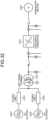
- FIG. 32 shows another example of a conventional FPC system.
- the FPC system When the capacity of an FPC system increases, the FPC system often needs to be connected to a bulk power system via a unit transformer.
- a generator motor 3202 is connected to one of two AC terminals of a frequency converter 3201.
- a first AC system (AC system 1) 3203 is connected to a high-voltage side terminal of a unit transformer 3207 via a first power line (power line 1) 3204, and a second AC system (AC system 2) 3205 is connected to the high-voltage side terminal of the unit transformer 3207 via a second power line (power line 2) 3206 to constitute a loop transmission system.
- the other AC terminal of the frequency converter 3201 is connected to a low-voltage side terminal of the unit transformer 3207.
- the first power line 3204 and the second power line 3206 are a direct grounded system or a high-resistance grounded system. Therefore, if a single line-to-ground fault occurs in any of the power lines, the terminal voltage of the unit transformer 3207 decreases, and a transient overcurrent occurs in the frequency converter 3201.
- the arc extinction capacity of the electronic switch constituting the frequency converter 3201 has been increased, and the DC capacitor capacity of the frequency converter has been increased.
- FPC systems have been exempted from continuing operation in the event of an in-phase single line-to-ground fault.
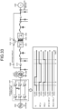
- a purpose of the present invention is to implement an FPC system applicable to the configuration shown in FIG. 33 .
- Another purpose of the present invention is to solve various problems to implement the FPC system with an electronic switch capacitance and DC capacitor capacitance smaller than those of a conventional frequency converter constituted by a conventional 3-level converter.
- a first 3-level converter 3301 and a second 3-level converter 3302 are connected back-to-back, and a positive capacitor 3303 and a negative capacitor 3304 are connected to the DC ends.
- a generator motor 3305 is connected to the AC end of the second 3-level converter 3302, and an AC system 3306 is connected to the AC end of the first 3-level converter 3301 via a single-circuit power line 3307 and a unit transformer 3308.
- the system side winding of the unit transformer 3308 is directly grounded or high resistance grounded.
- a circuit breaker 3310 is for protection in a variable speed operation mode via the 3-level converters, and a circuit breaker 3311 is for protection in a bypass operation mode via the bypass circuit 3309.
- the amplitude and the phase of the AC voltage of a second frequency converter 3302 are matched to the terminal voltage of the generator motor 3305, and a current command is rapidly increased to the generator current at the same time as the start of the operation of the frequency converter. This causes the current of the bypass circuit to rapidly approach zero, and it is possible to switch to the variable speed operation by opening a load breaker 3312 instead of the circuit breaker 3311.
- variable-speed operation mode is required to have the same or better operational continuity performance as the bypass operation mode.
- leading end circuit breaker (52F_A) is closed at time t3, and then the trailing end circuit breaker (52B_A) is closed at time t4.
- the period from time t2 to time t4 is called an open-phase period
- the single-circuit power line 3307 is for two-phase transmission for a B-phase and a C-phase while the A-phase is in an open-phase state.
- This open-phase period usually lasts nearly one second.
- Frequency converters have many advantages, but also have many disadvantages. Vulnerability in an open-phase period is the most serious disadvantage in applications in which frequency converters are connected to bulk power systems, including FPC systems.
- Patent Literature 2 a method of suppressing overcurrent in the electronic switch of a 3-level converter is disclosed in Patent Literature 2, which is applied to a doubly-fed induction machine.
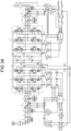
- a first 3-level converter 1 is provided with a positive terminal (P terminal) 2, a negative terminal (N terminal) 3, and an intermediate terminal (C terminal) 4 on the DC side, and provided with a U-phase terminal 5, a V-phase terminal 6, and a W-phase terminal 7 on the AC side.
- a second 3-level converter 8 is provided with a positive terminal (P terminal) 9, a negative terminal (N terminal) 10, and an intermediate terminal (C terminal) 11 on the DC side, and provided with a U-phase terminal 12, a V-phase terminal 13, and a W-phase terminal 14 on the AC side.
- a positive capacitor (CBP) 15 and a negative capacitor (CBN) 16 are provided at the back connection part on the DC side, and a positive discharge resistance (RP) 3401, a negative discharge resistance (RN) 3402, and a positive chopper (CHP) 3403 and a negative chopper (CHN) 3404 for preventing overcharge are provided.
- RP positive discharge resistance
- RN negative discharge resistance
- CHP positive chopper
- CHN negative chopper
- the AC side terminal of the first 3-level converter 1 is connected to an AC system 17 via a unit transformer 18, a circuit breaker with synchronous input device 19, and a harmonic filter 20 that also functions as a reactor.
- the AC terminal of the second 3-level converter 8 is connected to an electrical rotating machine 21 via a harmonic filter 22 that also functions as a reactor.
- an instrument transformer 23 is connected to the unit transformer 18 side, and an instrument transformer 24 is connected to the first 3-level converter 1 side.
- a signal of the instrument transformer 24 is input to a transformer-side phase detector 25, and a reference voltage phase signal ( ⁇ e) 26 is output.
- the reference voltage phase signal ( ⁇ e) 26 is input to a current regulator 3427.
- An instrument current transformer 28 that measures the AC current of the first 3-level converter 1 is provided between the circuit breaker with synchronous input device 19 and the harmonic filter 20.
- a signal of the instrument current transformer 28 is input to a power detector 29, and the power detector 29 outputs a reactive power signal (Q_FB) 30, which is matched with an external reactive power command (Q_REF) 31 and input to a reactive power regulator 32.
- Q_FB reactive power signal
- Q_REF external reactive power command
- a direct-axis current command (ITD_REF) 33 is output from the reactive power regulator 32 and input to the current regulator 3427.
- the voltage of the positive capacitor (CBP) 15 is measured by a DC voltage transformer 34, and the voltage of the negative capacitor (CBN) 16 is measured by a DC voltage transformer 35.
- a positive-side output signal (VDCP) 36 and a negative-side output signal (VDCN) 37 are energized to output a DC voltage signal (VC_FB) 38.
- the DC voltage signal (VC_FB) 38 is matched with an external DC voltage command (VC_REF) 39 and input to a DC voltage regulator 40, and the DC voltage regulator 40 outputs a transvers-axis current command (ITQ_REF) 41 and inputs it to the current regulator 3427.
- a U-phase current (ITU) 42, a V-phase current (ITV) 43, and a W-phase current (ITW) 44 from the instrument current transformer 28 are input to the current regulator 3427.
- the current regulator 3427 outputs a U-phase first mode command (M_TU1) 3445, a V-phase first mode command (M_TV1) 3446, and a W-phase first mode command (M_TW1) 3447.
- M_TU1 U-phase first mode command
- M_TV1 V-phase first mode command
- M_TW1 W-phase first mode command
- An output signal of a pulse generator 48 directly connected to the rotation shaft of the electrical rotating machine 21 is input to a rotation phase detector 49, and the rotation phase detector 49 outputs a rotation phase signal ( ⁇ r) 50 to a current regulator 3451.
- a voltage signal from an instrument transformer 52 provided between the electrical rotating machine 21 and the harmonic filter 22 and a current signal from an instrument current transformer 53 are input to a power detector 54.
- a reactive power signal (QM_FB) 55 from the power detector 54 and an external reactive power command (QM_REF) 56 are matched and input to a reactive power regulator 57, and a direct-axis current command (IMD_REF) 58 from the reactive power regulator 57 is input to the current regulator 3451.
- QM_FB reactive power signal
- QM_REF external reactive power command
- IMD_REF direct-axis current command
- the reactive power command (QM_REF) 56 is generally set to zero.
- An active power signal (P_FB) 65 from the power detector 29 and an external active power command (P_REF) 63 are matched and input to an active power regulator 3466, and a transvers-axis current command (IMQ_REF) 3467 is output and input to the current regulator 3451.
- a U-phase current (IMU) 76, a V-phase current (IMV) 77, and a W-phase current (IMW) 78 from the instrument current transformer 53 are input to the current regulator 3451.
- the current regulator 3451 outputs a U-phase mode command (M_MU) 3479, a V-phase mode command (M_MV) W-phase 3480, and a mode command (M_MW) 3481.
- M_MU U-phase mode command
- M_MV V-phase mode command
- M_MW mode command
- the 3-phase first mode commands 3445, 3446, and 3447 are input to a mode command switcher 3482.
- Current signals 42, 43, and 44 from the instrument current transformer 28 are input to the mode command switcher 3482 to calculate a second mode command, and a first mode command and a second mode command are selected to output a mode command (M_TU) 3483, a mode command (M_TV) 3484, and a mode command (M_TW) 3485 to the first 3-level converter 1.
- the 3-phase mode commands 3483, 3484, and 3485 are input to gate pulse generators 3486, 3487, and 3488, and 4-output gate pulses 3492, 3493, and 3494 are output, respectively.
- Mode commands 3479, 3480, and 3481 to the second 3-level converter 8 are input to gate pulse generators 3489, 3490, and 3491, and 4-output gate pulses 3495, 3496, and 3497 are output, respectively.
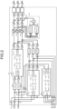
- a transvers-axis current (IQ) 207 from the 3-phase/2-phase calculator 205 and a transvers-axis current command (IQ_REF) 211 are matched and input to a transvers-axis current controller 212, and a transvers-axis voltage command (VQ_REF) 213 is output.
- IQ transvers-axis current
- VQ_REF transvers-axis voltage command
- the direct-axis current controller 209 and the transvers-axis current controller 212 each include at least proportional control elements and integral control elements, both of which are used in an activated state.
- a 2-phase/3-phase calculator 214 receives the phase reference signal ( ⁇ ) 201, the direct-axis voltage command (VD_REF) 210, and the transvers-axis voltage command (VQ_REF) 213, and outputs a U-phase voltage command first stage (VU1_REF) 215, a V-phase voltage command first stage (VV1_REF) 216, and a W-phase voltage command first stage (VW1_REF) 217.
- the 3-phase voltage command first stages 215, 216, and 217 are input to output limiters 3518, 3519, and 3520, and a U-phase voltage command third stage (VU3_REF) 3521, a V-phase voltage command third stage (VV3_REF) 3522, and a W-phase voltage command third stage (VW3_REF) 3523 are output, respectively.
- VU3_REF U-phase voltage command third stage
- VV3_REF V-phase voltage command third stage
- VW3_REF W-phase voltage command third stage
- An overmodulation suppression circuit 224 inputs the voltage command third stages 3521, 3522, and 3523 to a maximum-value selection circuit 225 and a minimum-value selection circuit 226, energizes outputs of the maximum-value selection circuit 225 and the minimum-value selection circuit 226, and outputs a voltage correction command 228 through a gain 227.
- a U-phase modulated-wave command ( ⁇ _U) 3529 is a signal obtained by subtracting the voltage correction command 228 from the U-phase voltage command third stage (VU3_REF) 3521.
- the U-phase modulated-wave command ( ⁇ _U) 3529 is input to a U-phase 3-level PWM modulator 3530, and a U-phase mode command (M_U) 3531 is output.
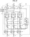
- a U-phase current (ITU) 3701, a V-phase current (ITV) 3702, a W-phase current (ITW) 3703 of the first 3-level converter are input.
- the effect of the mode command switcher 3482 is similar to the case in which the mode command switcher 3482 is applied to a doubly-fed induction machine, and it has been found that the overcurrent flowing through the electronic switches in the event of a system fault can be suppressed to be equal to or less than the first threshold (I1).
- the switch output (SW_TM) 3719 intermittently becomes level 1 and cannot return to the steady state.
- the reactive power signal (QM_FB) 55 from the power detector 54 and the external reactive power command (QM_REF) 56 are matched and input to the reactive power regulator 57, and the direct-axis current command (IMD_REF) 58 from the reactive power regulator 57 is input to the current regulator 51.
- QM_FB reactive power signal
- QM_REF external reactive power command
- IMD_REF direct-axis current command
- the auxiliary DC voltage regulator 61 branches and outputs the active power command correction ( ⁇ P_REF) 62, energizes it to an external speed command (N_REF) 72, matches it with a correction speed command 73 and the rotation speed signal (N_FB) 71 from the speed detector 70, and inputs it to a speed regulator 74.
- ⁇ P_REF active power command correction
- N_REF external speed command
- N_FB rotation speed signal
- the current regulator 51 outputs a mode command (M_MU) 79, a mode command (M_MV) 80, and a mode command (M_MW) 81.
- M_MU mode command
- M_MV mode command
- M_MW mode command
- An output limiter 218 limits upper and lower limits of the signal obtained by energizing the U-phase voltage command first stage (VU1_REF) 215 and the U-phase voltage command second stage (VU2_REF) 240, and outputs a U-phase voltage command third stage (VU3_REF) 221.
- the configurations for the V phase and the W phase are the same as that for the U phase, and the descriptions of output limiters 219 and 220 and voltage command third stages 222 and 223 are omitted to avoid duplication.
- An overmodulation suppression circuit 224 inputs the voltage command third stages 221, 222, and 223 to the maximum-value selection circuit 225 and the minimum-value selection circuit 226, energizes outputs of the maximum-value selection circuit 225 and the minimum-value selection circuit 226, and outputs the voltage correction command 228 through the gain 227.
- a U-phase modulated-wave command ( ⁇ _U) 229 is a signal obtained by subtracting the voltage correction command 228 from the U-phase voltage command third stage (VU3_REF) 221.
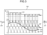
- the U-phase modulated-wave command ( ⁇ _U) 229 is input to a U-phase 3-level PWM modulator 230, and a U-phase mode command (M_U1) 231 is output.
- Modulated-wave commands 232 and 245, 3-level PWM modulators 233 and 246, and mode commands 234 and 247 for the V-phase and W-phase are also similar to those for the U-phase, and the descriptions thereof are omitted to avoid duplication.
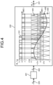
- the U-phase modulated-wave command ( ⁇ _U) 229 is input to an output regulator 401, and a modulated-wave correction command ( ⁇ _U) 402 is output.
- a modulated-wave correction command ( ⁇ _U) 402 is output.
- the U-phase mode command (M_U) 231 is output as level +1.
- the U-phase mode command (M_U) 231 is output as level -1. In other cases, the U-phase mode command (M_U) 231 is output as level 0.
- FIG. 5 is a diagram showing an embodiment of the mode command switcher 82 shown in FIG. 1 .
- the current signal (ITU) 42 from the instrument current transformer 28 is input to a comparator with hysteresis 502.
- a signal (SW_TUN) 504 is switched from level 0 to level 1.
- the signal (SW_TUN) 504 is switched from level 1 to level 0.
- the current signal (ITU) 42 from the instrument current transformer 28 is input to a comparator with hysteresis 503.
- a signal (SW_TUP) 505 is switched from level 0 to level 1.
- the signal (SW_TUP) 505 is switched from level 1 to level 0.
- the system-side circuit breaker operates in four cycles after the 3-phase ground fault occurs to remove the fault phase, and the remaining one-line transmission is performed.
- VDCP positive capacitor voltage signal
- VDCN negative capacitor voltage signal
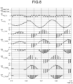
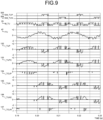
- FIGS. 8 and 9 are operation waveform diagrams for evaluating an overcurrent suppression effect.
- FIG. 8 shows a case in which the mode command switcher 82 is excluded, and
- FIG. 9 shows a case in which the operation is performed.
- the reference sign 42 is the U-phase current (ITU), and the positive side indicates the current in the outflow direction from the U-phase terminal of the first 3-level converter 1.
- a reference sign 102 is a U-phase P element current (I_TUP) of the first 3-level converter 1; the positive side indicates the current value of the electronic switch, and the negative side indicates the current value of the FWD.
- I_TUP U-phase P element current
- a reference sign 103 is a U-phase PC element current (I_TUPC) of the first 3-level converter 1; the positive side indicates the current value of the electronic switch, and the negative side indicates the current value of the FWD.
- I_TUPC U-phase PC element current
- Reference sign 104 is a U-phase P-side clamp diode current (I_TCUP) of the first 3-level converter 1, and a negative side indicates a current value of the diode.
- I_TCUP U-phase P-side clamp diode current
- a reference sign 105 is a U-phase N element current (I_TUN) of the first 3-level converter 1; the positive side indicates the current value of the electronic switch, and the negative side indicates the current value of the FWD.
- I_TUN U-phase N element current
- a reference sign 106 is a U-phase NC element current (I_TUNC) of the first 3-level converter 1; the positive side indicates the current value of the electronic switch, and the negative side indicates the current value of the FWD.
- I_TUNC U-phase NC element current
- a reference sign 107 is a U-phase N-side clamp diode current (I_TCUN) of the first 3-level converter 1, and a negative side indicates the current value of the diode.
- the impedance of the unit transformer 18 and a harmonic filter 28 is adjusted so that the current in the event of a fault is twice the current value in the steady state before the ground fault occurs at time 0.2 [s], in accordance with the design of a conventional standard 3-level converter.
- the signal (SW_TUP) 505 changes to level 1 twice by time 0.205 seconds.
- the threshold (I1) of the comparators with hysteresis 502 and 503 is set to 1.25 times the maximum current value during steady operation. Therefore, when the signal 505 rises to level 1, the U-phase current (ITU) is switched from the electronic switches of the N element and the NC element to the FWDs of the P element and the PC element, and the maximum current of the U-phase current (ITU) is reduced to 1.25 times from 2 times in FIG. 8 .
- the signal (SW_TUN) 504 changes to level 1 three times in a period from time 0.210 [s] to time 0.205 [s].
- the U-phase current (ITU) is switched from the electronic switches of the P element and the PC element to the FWDs of the N element and the NC element, and the maximum current of the U-phase current (ITU) is reduced to 1.25 times from 2 times in FIG. 8 .
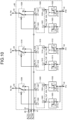
- a timer circuit 1006 receives the signal (SW_TUP) 1005 and the signal (SW_TUN) 1004 and outputs a U-phase second mode command (M_TU2) 1007 and a signal (SW_TU) 1008.
- a selector switch 1009 selectively outputs the U-phase first mode command (M_TU1) 45 when the signal (SW_TU) 1008 is level 0, and the U-phase second mode command (M_TU2) 1007 when the signal (SW_TU) 1008 is level 1 as the U-phase mode command (M_TU) 83.
- timer circuit 1006 An embodiment of the timer circuit 1006 is described with reference to FIG. 11 .
- the range of the signal 1004 (SW_TUN), the signal 1005 (SW_TUP), the signal 1014 (SW_TVN), the signal 1015 (SW_TVP), the signal 1024 (SW_TWN), the signal 1025 (SW_TWP), the U-phase mode command (M_TU) 83, the V-phase mode command (M_TV) 84, and the W-phase mode command (M_TW) 85 can be achieved only by the 2-level signal logical circuit and timer circuit, and there is an effect that the range can be achieved without being limited by the calculation cycle of a microprocessor. Therefore, it is possible to implement the first 3-level converter 1 suitable for small-capacity applications in which a high PWM frequency is often selected to downsize the system.
- An active power regulator 1366 matches and receives an active power signal (PM_FB) 1301 from the power detector 54 provided on the electrical rotating machine 21 side and the correction active power command 64, and outputs a signal 1367.
- a mode selector switch 1368 selectively outputs the output signal 1367 of the active power regulator 1366 and the output signal 75 of the speed regulator 74, and inputs the signal to the current regulator 51 as a transvers-axis current command (IMQ_REF) 1369.
- a mode selector switch 1468 selectively outputs the output signal 1467 of the active power regulator 1466 and the output signal 1475 of the speed regulator 1474 as a signal 1469.
- the match signal (VC_DIF) 59 of the DC voltage signal (VC_FB) 38 and the DC voltage command (VC_REF) 39 is input to a dead band gain 1460, and the input to an auxiliary DC voltage regulator 1461 is a value other than zero when the absolute value of deviation exceeds a threshold.
- the auxiliary DC voltage regulator 1461 outputs a transvers-axis current command correction ( ⁇ IMQ_REF) 1462, energizes it to the signal 1469 from the mode selector switch 1468, and inputs it to the current regulator 51 as a transvers-axis current command (IMQ_REF) 1470.
- the transvers-axis current command correction ( ⁇ IMQ_REF) 1462 energizes the transvers-axis current command (IMQ_REF) 1470 to the electrical rotating machine 21 in the power generation direction when the match signal (VC_DIF) 59 is positive and the DC voltage signal (VC_FB) 38 is lower than the DC voltage command (VC_REF) 39, and energizes the transvers-axis current command (IMQ_REF) 1470 in the electric direction when the match signal (VC_DIF) 59 is negative.
- the transvers-axis current command (IMQ_REF) 1470 obtained by energizing the transvers-axis current command correction ( ⁇ IMQ_REF) 1462 to the signal 1469 from the mode selector switch 1468 is directly input to the current regulator 51, there is an effect of suppressing and recovering the capacitor voltage signal (VC_DIF) 59 at a high speed particularly when the speed regulator 1474 is used.
- FIGS. 15 and 16 An embodiment according to Claim 2 of the present invention is described with reference to FIGS. 15 and 16 .
- FIG. 15 shows the state transition of a mode command (M) 1511, which is one input to the gate pulse generators 86, 87, and 88, and four outputs of a gate pulse (G_P) 1512, an output gate pulse (G_PC) 1513, an output gate pulse (G_NC) 1514, and an output gate pulse (G_N) 1515.
- M mode command
- the four element currents 1604, 1607, 1611, and 1614 indicate the current between the collector and emitter of the electronic switch in the positive direction and the current between the anode and cathode of the FWD in the negative direction.
- the two clamp diode currents 1608 and 1615 indicate the currents in the negative direction.
- the four gate currents 1603, 1606, 1610, and 1613 indicate the currents in the positive direction during turn-on and in the negative direction during turn-off.
- the dead time compensation period Td2 in the 1521 state is set to be longer than the dead time set period Td1 of 1519 and 1520.
- the voltage imbalance suppression operation by the mode command switcher 1702 is sporadically performed on the system side before the 3-phase ground fault occurs at time 0.2 [s]. Since the 3-phase ground fault at time 0.2 [s] is a symmetrical fault, the signals (SW_MU) 1816, 1826 (SW_MV), and 1836 (SW_MW) alternate at approximately the same frequency, but the operation is completed within three cycles after the fault phase is removed, and the imbalance between the positive capacitor voltage signal (VDCP) 36 and the negative capacitor voltage signal (VDCN) 37 seen in FIG. 6 converges.
- the mode switcher 1702 uses the relatively smooth current command (IMU_REF) 1704 instead of the current (IMU) 76 of the second 3-level converter 8 including the pulsation component, the operation frequency of the mode switcher 1702 is minimized. Therefore, there is an effect of maintaining independence from other control operations. In addition, by suppressing the operation frequency of the mode switcher 1702, there is an effect of minimizing the number of switching operations of the electronic switch and the FWD, thereby suppressing the increase in generated losses.
- IMU_REF relatively smooth current command
- the U-phase first mode command (M_MU1) 1779, the V-phase first mode command (M_MV1) 1780, and the W-phase first mode command (M_MW1) 1781 from the current regulator 1701 are input.
- the voltage signal (VDCP) 36 of the positive capacitor (CBP) 15 and the voltage signal (VDCN) 37 of the negative capacitor (CBN) 16 are input.
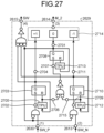
- a signal 2707 becomes level 1
- a flip-flop circuit 2708 is set, the signal 2701 becomes level 1, and the second mode command (M_2) 2614 becomes level 0 by an output switching circuit 2714.
- FIG. 28 a period from time t1 to time t8 indicates the operation according to Claim 5
- a period from time t9 to time t14 indicates the operation according to Claim 6.
- FIG. 29 shows an embodiment in a case where Claim 5 of the present invention is applied to the timer circuit 1814.
- a reference sign 2924 is an output switching circuit.
- the output switching circuit 2924 sets the second mode command (M_2) 1815 to level 0 and outputs it when a signal 2901 is level 1, sets the second mode command (M_2) 1815 to level +1 and outputs it when a signal 2902 is level 1, and sets the second mode command (M_2) 1815 to level -1 and outputs it when a signal 2903 is level 1.
- the output signal 2906 of the flip-flop circuit 2905 becomes level 0.
- the signal 2901 also becomes level 0.
- the signal 2902 becomes level 1, and the mode command (M_2) 1815 is switched from level 0 to level +1.
- the signal (SW_P) 1812 when the signal (SW_P) 1812 is level 0, the signal (SW) 1816 becomes level 0.
- the signal (SW) 1816 is an OR output of the signals 2901, 2902, and 2903.
- the input signal (SW_P) 2630 is level 0
- the signal (SW) 2615 changes from level 1 to level 0.
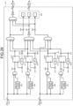
- a reference sign 3060 is an output switching circuit.
- the output switching circuit 3060 sets the second mode command (M_2) 2614 to level 0 and outputs it when a signal 3001 is level 1, sets the second mode command (M_2) 2614 to level +1 and outputs it when a signal 3020 is level 1, and sets the second mode command (M_2) 2614 to level -1 and outputs it when a signal 3040 is level 1.
- a signal 3022 becomes level 1 by a previous-value holding circuit 3021.
- a logical conjunction signal 3023 of the signal 3022 and the input signal (SW_P) 2630 sets a flip-flop circuit with reset priority 3024.
- the input signal (SW_P) 2630 is level 1
- the signal 3020 becomes level 1
- the output switching circuit 3060 outputs level +1 as the second mode command (M_2) 2614.
- a signal 3028 becomes level 1 by a previous-value holding circuit 3027. Since an output signal 3030 of a flip-flop circuit with reset priority 3029 becomes level 1 and the signal 3001 becomes level 1, the output switching circuit 3060 outputs level 0 as the second mode command (M_2) 2614.
- the output signal 3030 of the flip-flop circuit 3029 becomes level 0 after the set time Td2 of the on-delay circuit 3031, and the signal 3001 also becomes level 0.
- the signal (SW) 2615 is an OR output of the signals 3001, 3020, and 3040, and outputs level 1 when the second mode command (M_2) 2614 is enabled.
Landscapes
- Engineering & Computer Science (AREA)
- Power Engineering (AREA)
- Inverter Devices (AREA)
Abstract
Description
- The present invention relates to a neutral point clamped 3-level semiconductor power converter (hereinafter, referred to as a "3-level converter" in the present invention). The present invention particularly relates to an adjustable speed generator motor system with full power converter (hereinafter, referred to as an FPC system) in which the direct current (DC) sides of two 3-level converters are connected back-to-back to constitute a frequency converter, the alternating current (AC) side of one 3-level converter is connected to a power system, and the AC side of the other 3-level converter is connected to an AC rotating machine (hereinafter, referred to as an electrical rotating machine).
- 3-level converters are applied to variable speed drives of electric motors, power converters for solar power generation facilities, and frequency converters used for variable speed of hydraulic, pumped storage, and wind power generation facilities.
- There are two types for variable speed for hydraulic, pumped storage, and wind power generation facilities. The first type is a doubly-fed induction machine in which a frequency converter is connected between a low-voltage side terminal of a unit transformer whose high-voltage side terminal is connected to an AC system and an excitation winding terminal of a wound rotor induction machine.
- The second type is an FPC system in which a frequency converter is connected between a low-voltage side terminal of a unit transformer and an armature winding terminal of a generator motor. 3-level converters are applied in both types.
- Since recent technological advances in self arc-extinguishing semiconductor devices (hereinafter, referred to as "electronic switches" in the present invention) and diodes have led to higher withstand voltage and lower power dissipation, the application range of 3-level converters continues to expand.
- In particular, improvements in the price performance ratio of frequency converters have expanded the applications of FPC systems. Meanwhile, the overcurrent capacity of a self-commutated power converter employing an electronic switch, such as a 3-level converter, has a disadvantage of being limited by the instantaneous current value at turn-off switching.
- For this reason, a method including an arc-extinguishing current capacity that withstands overcurrent generated at a power line failure and a method applying bypass switch circuit are generally used.
- The former method has a disadvantage of causing an increase in size of the system, and the latter method has a disadvantage of significantly shaking the AC system.
- Regarding a doubly-fed induction system, a method of commutating current to a fly-wheeling diode (hereinafter, referred to as an FWD) an arc-extinguishing current capacity of an electronic switch is exceeded is disclosed when a 2-level power converter is employed in
Patent Literature 1 and when a 3-level converter is employed inPatent Literature 2. -
- Patent Literature 1:
JP 5401213 B - Patent Literature 2:
WO 2020/230343 A - Patent Literature 3:
WO 2019/235595 A - Patent Literature 4:
JP 2020-195226 A - Patent Literature 5:
JP 5952087 B - A conventional generator motor system is connected to armature winding terminals of a generator motor via an AC system and a unit transformer, and a rotor phase is constrained by power line voltage phase via synchronizing power coefficient. Thus, rotating speed is fixed at synchronous speed. Compared with a conventional generator motor, an FPC system has many advantages.
- When FPC systems are applied to hydraulic, wind, and other power generation facilities, the purpose is often to improve system efficiency, including turbine efficiency, through variable speed operation.
- Therefore, in order to achieve the purpose of employing FPC systems, the main premise is to reduce the dimensions and price of a frequency converter, which is an additional facility associated with variable speed.
- From the above perspective, the basic design of a 2-level power converter or a 3-level converter, which has been used as a commercially-available variable-speed electric device for production facilities in factories, is often diverted as a frequency converter of an FPC system.
-
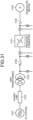
FIG. 31 shows an example of a conventional FPC system. Agenerator motor 3102 is connected to one of two AC terminals of afrequency converter 3101 via adisconnector switch 3103 for maintenance. - The other AC terminal of the
frequency converter 3101 is connected to anAC system 3107 via apower line 3104, aunit transformer 3105, and a circuit breaker withsynchronous input device 3106. - Since the
conventional frequency converter 3101 is based on a design for applications connected to a factory power supply, the system side winding of theunit transformer 3105 is assumed to be a delta winding, and thepower line 3104 is often a non-grounded system. - When the
power line 3104 is a grounded system or a high-resistance grounded system, thefrequency converter 3101 is not affected by transient phenomena during single line-to-ground faults that account for the majority of ground faults occurring in thepower line 3104. For this reason, non-grounded power lines are used intendedly. - In practice, the system-side terminal voltage of the
unit transformer 3105 drops to almost zero, including when symmetrical faults occur on thepower line 3104. In such cases, the Grid Code enacted to ratify the expansion of applications of wind and solar power generation facilities that cannot actually continue operation has been used as a remedy, and the existing facilities have been exempted from continuing operation. -
FIG. 32 shows another example of a conventional FPC system. When the capacity of an FPC system increases, the FPC system often needs to be connected to a bulk power system via a unit transformer. - A
generator motor 3202 is connected to one of two AC terminals of afrequency converter 3201. A first AC system (AC system 1) 3203 is connected to a high-voltage side terminal of aunit transformer 3207 via a first power line (power line 1) 3204, and a second AC system (AC system 2) 3205 is connected to the high-voltage side terminal of theunit transformer 3207 via a second power line (power line 2) 3206 to constitute a loop transmission system. - The other AC terminal of the
frequency converter 3201 is connected to a low-voltage side terminal of theunit transformer 3207. - Here, the
first power line 3204 and thesecond power line 3206 are a direct grounded system or a high-resistance grounded system. Therefore, if a single line-to-ground fault occurs in any of the power lines, the terminal voltage of theunit transformer 3207 decreases, and a transient overcurrent occurs in thefrequency converter 3201. - In order to continue operation in the event of spreading a fault on the system side, the arc extinction capacity of the electronic switch constituting the
frequency converter 3201 has been increased, and the DC capacitor capacity of the frequency converter has been increased. - When the
first AC system 3203 and thesecond AC system 3205 are common, thefirst power line 3204 and thesecond power line 3206 constitute a double-circuit power line and are connected to a longitudinal transmission system. - In any case, the probability of occurrence of an in-phase single line-to-ground fault, in which a ground fault occurs simultaneously in the same specific phase of the
first power line 3204 and thesecond power line 3206, has been regarded as extremely low. - FPC systems have been exempted from continuing operation in the event of an in-phase single line-to-ground fault. Alternatively, even in the case of a double-circuit power line, if one circuit cannot be used for maintenance inspection or the like, an open-phase operation period occurs due to high-speed reclosing in the event of a single line-to-ground fault, and the system in this case had to be exempted from continuing operation.
- As described above, the "operation continuation exemption based on the Grid Code" and the "operation continuation exemption in the event of an open-phase operation period" are caused by "weaknesses of frequency converters using electronic switches" and have been regarded as indispensable.
- Meanwhile, in generator motor systems that do not use frequency converters, it is compulsorily required to continue operation in the event of a close-end ground fault in which a system end voltage of a unit transformer drops to zero or in the event of an in-phase single line-to-ground fault.
- A purpose of the present invention is to implement an FPC system applicable to the configuration shown in
FIG. 33 . - Another purpose of the present invention is to solve various problems to implement the FPC system with an electronic switch capacitance and DC capacitor capacitance smaller than those of a conventional frequency converter constituted by a conventional 3-level converter.
- Hereinafter,
FIG. 33 is described. - A first 3-
level converter 3301 and a second 3-level converter 3302 are connected back-to-back, and apositive capacitor 3303 and anegative capacitor 3304 are connected to the DC ends. - A
generator motor 3305 is connected to the AC end of the second 3-level converter 3302, and anAC system 3306 is connected to the AC end of the first 3-level converter 3301 via a single-circuit power line 3307 and aunit transformer 3308. The system side winding of theunit transformer 3308 is directly grounded or high resistance grounded. - In the configuration in
FIG. 33 , the AC ends of the two 3-level converters bypass circuit 3309 is provided between theunit transformer 3308 and thegenerator motor 3305. - A
circuit breaker 3310 is for protection in a variable speed operation mode via the 3-level converters, and acircuit breaker 3311 is for protection in a bypass operation mode via thebypass circuit 3309. -
Patent Literatures generator motor 3305. - When the bypass operation is switched to the variable speed operation, the amplitude and the phase of the AC voltage of a
second frequency converter 3302 are matched to the terminal voltage of thegenerator motor 3305, and a current command is rapidly increased to the generator current at the same time as the start of the operation of the frequency converter. This causes the current of the bypass circuit to rapidly approach zero, and it is possible to switch to the variable speed operation by opening aload breaker 3312 instead of thecircuit breaker 3311. - In order to switch from the variable speed operation to the bypass operation, by adjusting the rotation speed to the synchronous speed by the active power regulation, adjusting the voltage amplitude and phase of both ends of the
load breaker 3312 by the voltage phase regulation to close theload breaker 3312, rapidly narrowing the current of the frequency converter to zero, and stopping the operation, it is possible to switch to the bypass operation. - In the case of the configuration in
FIG. 33 , it is practically impossible to distinguish the operation mode from the outside. There is no rational reason, either from the perspective of the owner of an FPC system or from the perspective of the operator of a power system, to distinguish between the variable speed operation mode and the bypass operation mode for operation when a ground fault occurs on the system side. - Therefore, in the event of a single line-to-ground fault, which accounts for the majority of system-side ground faults, the variable-speed operation mode is required to have the same or better operational continuity performance as the bypass operation mode.
- A typical time chart when a single line-to-ground fault occurs in the single-
circuit power line 3307 is shown. - Hereinafter, an example in which an A-phase single line-to-ground fault occurs at time t1 in the configuration in
FIG. 33 is described. At time t2, a leading end circuit breaker (52F_A) and a trailing end circuit breaker (52B_A) for the A-phase are opened. - The leading end circuit breaker (52F_A) is closed at time t3, and then the trailing end circuit breaker (52B_A) is closed at time t4.
- As a result, the period from time t2 to time t4 is called an open-phase period, and the single-
circuit power line 3307 is for two-phase transmission for a B-phase and a C-phase while the A-phase is in an open-phase state. This open-phase period usually lasts nearly one second. - Frequency converters have many advantages, but also have many disadvantages. Vulnerability in an open-phase period is the most serious disadvantage in applications in which frequency converters are connected to bulk power systems, including FPC systems.
- As disclosed above, a method of suppressing overcurrent in the electronic switch of a 3-level converter is disclosed in
Patent Literature 2, which is applied to a doubly-fed induction machine. - The application of this method to an FPC system is shown in
FIG. 34 . - A first 3-
level converter 1 is provided with a positive terminal (P terminal) 2, a negative terminal (N terminal) 3, and an intermediate terminal (C terminal) 4 on the DC side, and provided with aU-phase terminal 5, a V-phase terminal 6, and a W-phase terminal 7 on the AC side. A second 3-level converter 8 is provided with a positive terminal (P terminal) 9, a negative terminal (N terminal) 10, and an intermediate terminal (C terminal) 11 on the DC side, and provided with aU-phase terminal 12, a V-phase terminal 13, and a W-phase terminal 14 on the AC side. - A positive capacitor (CBP) 15 and a negative capacitor (CBN) 16 are provided at the back connection part on the DC side, and a positive discharge resistance (RP) 3401, a negative discharge resistance (RN) 3402, and a positive chopper (CHP) 3403 and a negative chopper (CHN) 3404 for preventing overcharge are provided.
- The AC side terminal of the first 3-
level converter 1 is connected to anAC system 17 via aunit transformer 18, a circuit breaker withsynchronous input device 19, and aharmonic filter 20 that also functions as a reactor. - The AC terminal of the second 3-
level converter 8 is connected to an electricalrotating machine 21 via aharmonic filter 22 that also functions as a reactor. - At both ends of the circuit breaker with
synchronous input device 19, aninstrument transformer 23 is connected to theunit transformer 18 side, and aninstrument transformer 24 is connected to the first 3-level converter 1 side. A signal of theinstrument transformer 24 is input to a transformer-side phase detector 25, and a reference voltage phase signal (θe) 26 is output. The reference voltage phase signal (θe) 26 is input to acurrent regulator 3427. - An instrument
current transformer 28 that measures the AC current of the first 3-level converter 1 is provided between the circuit breaker withsynchronous input device 19 and theharmonic filter 20. A signal of the instrumentcurrent transformer 28 is input to apower detector 29, and thepower detector 29 outputs a reactive power signal (Q_FB) 30, which is matched with an external reactive power command (Q_REF) 31 and input to areactive power regulator 32. A direct-axis current command (ITD_REF) 33 is output from thereactive power regulator 32 and input to thecurrent regulator 3427. - The voltage of the positive capacitor (CBP) 15 is measured by a
DC voltage transformer 34, and the voltage of the negative capacitor (CBN) 16 is measured by aDC voltage transformer 35. A positive-side output signal (VDCP) 36 and a negative-side output signal (VDCN) 37 are energized to output a DC voltage signal (VC_FB) 38. The DC voltage signal (VC_FB) 38 is matched with an external DC voltage command (VC_REF) 39 and input to aDC voltage regulator 40, and theDC voltage regulator 40 outputs a transvers-axis current command (ITQ_REF) 41 and inputs it to thecurrent regulator 3427. - A U-phase current (ITU) 42, a V-phase current (ITV) 43, and a W-phase current (ITW) 44 from the instrument
current transformer 28 are input to thecurrent regulator 3427. - The
current regulator 3427 outputs a U-phase first mode command (M_TU1) 3445, a V-phase first mode command (M_TV1) 3446, and a W-phase first mode command (M_TW1) 3447. - An output signal of a
pulse generator 48 directly connected to the rotation shaft of the electricalrotating machine 21 is input to arotation phase detector 49, and therotation phase detector 49 outputs a rotation phase signal (θr) 50 to acurrent regulator 3451. - A voltage signal from an
instrument transformer 52 provided between the electricalrotating machine 21 and theharmonic filter 22 and a current signal from an instrumentcurrent transformer 53 are input to apower detector 54. A reactive power signal (QM_FB) 55 from thepower detector 54 and an external reactive power command (QM_REF) 56 are matched and input to areactive power regulator 57, and a direct-axis current command (IMD_REF) 58 from thereactive power regulator 57 is input to thecurrent regulator 3451. - Since the electrical
rotating machine 21 maximizes efficiency at a power factor of 1, the reactive power command (QM_REF) 56 is generally set to zero. - An active power signal (P_FB) 65 from the
power detector 29 and an external active power command (P_REF) 63 are matched and input to anactive power regulator 3466, and a transvers-axis current command (IMQ_REF) 3467 is output and input to thecurrent regulator 3451. A U-phase current (IMU) 76, a V-phase current (IMV) 77, and a W-phase current (IMW) 78 from the instrumentcurrent transformer 53 are input to thecurrent regulator 3451. - The
current regulator 3451 outputs a U-phase mode command (M_MU) 3479, a V-phase mode command (M_MV) W-phase 3480, and a mode command (M_MW) 3481. - The 3-phase first mode commands 3445, 3446, and 3447 are input to a
mode command switcher 3482.Current signals current transformer 28 are input to themode command switcher 3482 to calculate a second mode command, and a first mode command and a second mode command are selected to output a mode command (M_TU) 3483, a mode command (M_TV) 3484, and a mode command (M_TW) 3485 to the first 3-level converter 1. The 3-phase mode commands 3483, 3484, and 3485 are input togate pulse generators 3486, 3487, and 3488, and 4-output gate pulses - Mode commands 3479, 3480, and 3481 to the second 3-
level converter 8 are input togate pulse generators 3489, 3490, and 3491, and 4-output gate pulses -
FIG. 35 shows a current regulator and shows a configuration of thecurrent regulator 3427 of the first 3-level converter 1 and thecurrent regulator 3451 of the second 3-level converter 8. - A 3-phase/2-
phase calculator 205 receives a phase reference signal (θ) 201, a U-phase current (IU) 202, a V-phase current (IV) 203, and a W-phase current (IW) 204. A direct-axis current (ID) 206 from the 3-phase/2-phase calculator 205 and a direct-axis current command (ID_REF) 208 are matched and input to a direct-axiscurrent controller 209, and a direct-axis voltage command (VD_REF) 210 is output. - In addition, a transvers-axis current (IQ) 207 from the 3-phase/2-
phase calculator 205 and a transvers-axis current command (IQ_REF) 211 are matched and input to a transvers-axiscurrent controller 212, and a transvers-axis voltage command (VQ_REF) 213 is output. - Here, the direct-axis
current controller 209 and the transvers-axiscurrent controller 212 each include at least proportional control elements and integral control elements, both of which are used in an activated state. - A 2-phase/3-
phase calculator 214 receives the phase reference signal (θ) 201, the direct-axis voltage command (VD_REF) 210, and the transvers-axis voltage command (VQ_REF) 213, and outputs a U-phase voltage command first stage (VU1_REF) 215, a V-phase voltage command first stage (VV1_REF) 216, and a W-phase voltage command first stage (VW1_REF) 217. The 3-phase voltage command first stages 215, 216, and 217 are input tooutput limiters - An
overmodulation suppression circuit 224 inputs the voltage commandthird stages value selection circuit 225 and a minimum-value selection circuit 226, energizes outputs of the maximum-value selection circuit 225 and the minimum-value selection circuit 226, and outputs avoltage correction command 228 through again 227. - A U-phase modulated-wave command (α_U) 3529 is a signal obtained by subtracting the
voltage correction command 228 from the U-phase voltage command third stage (VU3_REF) 3521. The U-phase modulated-wave command (α_U) 3529 is input to a U-phase 3-level PWM modulator 3530, and a U-phase mode command (M_U) 3531 is output. - Modulated-
wave commands level PWM modulators -
FIG. 36 shows a configuration of a gate pulse generator.Fig 36 shows the configuration of thegate pulse generators 3486, 3487, 3488 of the first 3-level converter 1 and thegate pulse generators 3489, 3490, 3491 of the second 3-level converter 8. - A mode command M to the gate pulse generators has 3-levels of +1, 0, and -1. The electronic switches in four series constituting the 3-level converter are referred to as a P element, a PC element, an NC element, and an N element in order from the DC positive terminal P to the negative terminal N, and the gate outputs to the respective elements are denoted as G_P, G_PC, G_NC, and G_N.
- When the mode command M is level +1, G_P and G_PC are ON output, and G_N and G_NC are OFF output.
- When the mode command M is
level 0, G_PC and G_NC are ON output, and G_P and G_N are OFF output. - When the mode command M is level -1, G_N and G_NC are ON output, and G_P and G_PC are OFF output.
-
FIG. 37 shows a configuration of a mode command switcher of a doubly-fed induction 3-level converter disclosed inPatent Literature 2, which is themode command switcher 3482. - A U-phase current (ITU) 3701, a V-phase current (ITV) 3702, a W-phase current (ITW) 3703 of the first 3-level converter are input.
- Absolute-
value calculation circuits detectors level 1 when the absolute value of the U-phase current (ITU) 3701 is minimum, a comparison result (SW_TV) 3711 islevel 1 when the absolute value of the V-phase current (ITV) 3702 is minimum, and a comparison result (SW_TW) 3712 islevel 1 when the absolute value of the W-phase current (ITW) 3703 is minimum. -
Reference signs sign detector 3713 outputs level +1 as a U-phase second mode command (M_TU2) 3731 when the U-phase current (ITU) 3701 is negative and the absolute value is not minimum, and outputs level -1 as the second mode command (M_TU2) 3731 when the U-phase current (ITU) 3701 is positive and the absolute value is not minimum. In addition, thesign detector 3713outputs level 0 as the second mode command (M_TU2) 3731 when the absolute value of the U-phase current (ITU) 3701 is minimum. - A V-phase second mode command (M_TV2) 3732 and a W-phase second mode command (M_TW2) 3733 are output with the same configuration and operation as those for the U-phase, and the descriptions thereof are omitted to avoid duplication.
- A maximum-
value selection circuit 3716 inputs a maximum value (CIMAX) 3717 of the 3-phase current absolute values to a comparator withhysteresis 3718. The comparator withhysteresis 3718 changes a switch output (SW_TM) 3719 fromlevel 0 tolevel 1 when the maximum value (CIMAX) 3717 of the 3-phase current absolute values exceeds a first threshold (I1), and fromlevel 1 tolevel 0 when the maximum value (CIMAX) 3717 falls below a second threshold (I2). - A U-phase first mode command (M_TU1) 3720 and a second mode command (M_TU2) 3731 are switched by a U-phase
mode selector switch 3723. The U-phasemode selector switch 3723 selectively outputs the U-phase first mode command (M_TU1) 3720 as a mode command (M_TU) 3726 when the switch output (SW_TM) 3719 islevel 0, and selectively outputs the U-phase second mode command (M_TU2) 3731 as the mode command (M_TU) 3726 when the switch output (SW_TM) 3719 islevel 1. - A
selector switch 3724, which switches a V-phase first mode command (M_TV1) 3721 and a V-phase second mode command (M_TV2) 3732 and outputs a mode command (M_TV) 3727, and aselector switch 3725, which switches a W-phase first mode command (M_TW1) 3722 and a W-phase second mode command (M_TW2) 3733 and outputs a mode command (M_TW) 3728 are also similar to that for the U-phase, and the descriptions thereof are omitted to avoid duplication. - In the configuration in
FIG. 37 , the 3-phase mode commands are simultaneously switched by the switch output (SW_TM) 3719. - In the case of the FPC system in
FIGS. 34 ,35 ,36 , and37 , the effect of themode command switcher 3482 is similar to the case in which themode command switcher 3482 is applied to a doubly-fed induction machine, and it has been found that the overcurrent flowing through the electronic switches in the event of a system fault can be suppressed to be equal to or less than the first threshold (I1). However, even after the system fault is ended, the switch output (SW_TM) 3719 intermittently becomeslevel 1 and cannot return to the steady state. Therefore, when the switch output (SW_TM) 3719 is forcibly fixed tolevel 0 with a time limit, the overcurrent flowing through the electronic switches immediately after the switch output (SW_TM) is fixed tolevel 0 exceeds the first threshold (I1), and a current exceeding the first threshold (I1) must be extinguished. - In general, an electronic switch that extinguishes a current exceeding an element specific threshold even once is considered to be broken or damaged. For this reason, it has been found that the configuration in
FIG. 37 is effective for a doubly-fed induction system but is not applicable to an FPC system in which a frequency converter is connected to the primary armature side of a generator motor. - In order to solve the above problem and implement a 3-level converter that stably continues operation after a system fault while suppressing overcurrent of an FPC system, a method of switching mode commands independently for three phases is conceivable.
- However, new problems arise in switching mode commands independently for three phases. A first problem is that overcurrent cannot be suppressed in the event of an asymmetrical fault on the system side. A second problem is that voltage imbalance occurs between capacitors on the positive side and the negative side of a 3-level converter.
- Purposes of the present invention are to solve the above problems to employ a 3-level converter and to provide an FPC system that is compact and lightweight by removing a discharge resistance or minimizing the discharge resistance capacity and secures operational continuity in the event of a system fault.
- In order to achieve the above purposes, the current control of a 3-level converter is performed while switching mode commands independently for three phases to suppress overcurrent in all the three phases. The suppression of current imbalance between the three phases is achieved by providing a second current controller independently for three phases and energizes it to a first current controller. The second current controller consists only of proportional gain and excludes integral gain elements.
- Since the sum of the proportional gain elements of the first current controller and the proportional gain elements of the second current controller is limited by the time constant of a control target of a current control system and the calculation cycle of the control system, allocation is important. In the case of suppressing overcurrent independently for three phases, it has been found that by setting the proportional gain elements of the second current controller to four times or more the proportional gain elements of the first current controller, the stability of the current control can be secured even if the capacitor capacitance is reduced to 1/2 or less in the event of a symmetrical fault on the power line side and to 1/4 or less in the event of an asymmetrical fault with an open-phase period, compared with the case of only the first current controller.
- In the case of suppressing overcurrent while switching mode commands independently for three phases, the voltage output waveform of the 3-level converter becomes the output voltage waveform of a 2-level power converter with two elements in series. Then, the turn-off time of the electronic switch becomes longer, and it is necessary to set the dead time longer, which is a problem that the current control characteristic during the normal operation is deteriorated.
- In order to solve the problem, a dead time compensation circuit is provided at a subsequent stage of mode command switching, and the dead time is set longer only at the time of the overcurrent suppression operation.
- In addition, switching mode commands for the current control of the 3-level converter independently for three phases arises a new problem of rapidly expanding voltage imbalance between the positive capacitor and the negative capacitor.
-
Patent Literature 5 and the like disclose a method for suppressing voltage imbalance between the positive capacitor and the negative capacitor. - However, in order to stably operate in the event of an asymmetrical fault on the system side, a simple method that does not require complicated calculation is required.
- The solution of this problem is achieved by switching to a second mode command according to the signs (direction) of the 3-phase currents and the magnitude relation to suppress the voltage imbalance between the positive capacitor and the negative capacitor while switching the mode commands of the 3-level converter for current control independently for three phases.
- In addition, the solution is achieved by switching the mode command of the 3-level converter connected to the generator motor side in which the influence of the system side fault spreading is relatively small.
- Hereinafter, a second mode command switching method is described.
- In general, the charging currents of the positive capacitor and the negative capacitor of the 3-level converter are inverted in magnitude relation even during normal operation, and the capacitor voltage is pulsating.
- In a conduction mode of the 3-level converter shown in
FIG. 38 , the U phase and the W phase have positive currents, and the V phase has a negative current of a total value of the U phase and the W phase. In this case, the charging current of the positive capacitor is a total current value of the V phase and the W phase. The charging current of the negative capacitor is the V-phase current value. In the conduction mode, the difference between the positive capacitor voltage and the negative capacitor voltage (VDCP-VDCN) changes to the positive side. - In a conduction mode of the 3-level converter shown in
FIG. 39 , the V phase and the W phase have negative currents, and the U phase has a positive current of a total value of the V phase and the W phase. In this case, the charging current of the negative capacitor is a total current value of the V phase and the W phase. The charging current of the positive capacitor is the V-phase current value. In the conduction mode, the difference between the positive capacitor voltage and the positive capacitor voltage (VDCP-VDCN) changes to the negative side. -
FIG. 40 shows a change in the difference between the positive capacitor voltage and the negative capacitor voltage (VDCP-VDCN) of the 3-level converter. Assuming that one cycle is 360 degrees, one cycle is divided into 12 modes every 30 degrees.FIG. 38 corresponds tomode number 1, andFIG. 39 corresponds tomode number 2. - According to the determination criteria shown in
FIG. 40 , when the absolute value of the difference between the positive capacitor voltage and the negative capacitor voltage (VDCP-VDCN) exceeds a threshold, the current conduction mode is determined by the 3-phase current value or the 3-phase current command value, and the mode is switched to the required mode command when the mode becomes for reducing the voltage imbalance. - The positive capacitor voltage and the negative capacitor voltage are common to the first 3-level converter and the second 3-level converter connected back-to back on the DC side. Therefore, it can be achieved by switching the mode command of either 3-level converter.
- In the case of the FPC system, since the mode switching is prioritized for the overcurrent suppression on the first 3-level converter side which is directly affected by the system side, suppression of the voltage imbalance between the positive and negative capacitors is achieved by switching the mode command on the second 3-level converter side connected to the generator motor side.
- The mode command switching due to the suppression of the voltage imbalance between the positive and negative capacitors does not simultaneously operate in two or more phases.
- However, the stability can be enhanced by providing the second current controller independently for three phases on the second 3-level converter side and energizing it to the first current controller.
- It has been found that when the positive and negative capacitor voltage imbalance is suppressed by the mode command switching, the voltage waveform of the second power converter becomes the output voltage waveform of the 2-level power converter with two elements in series as in the case of the overcurrent suppression.
- The second power converter is connected to the electrical rotating machine. The purpose of employing the 3-level converter instead of the 2-level power converter is to protect the insulation of the electrical rotating machine coil by suppressing the step change width of the voltage waveform and the time change rate of the voltage. Therefore, it is desirable to avoid the output voltage waveform of the 2-level power converter.
- This problem can be solved by providing a period of the
voltage level 0 before and after the period of the mode command switching in order to suppress the capacitor voltage imbalance. - The desired purposes can be achieved by the above system configuration and control method.
- According to an FPC system of the present invention, while reducing the current capacity of semiconductor elements constituting a 3-level converter and suppressing the positive and negative capacitor capacitances, it is possible to secures better performance than a conventional fixed-speed generator motor system in terms of operational continuity performance during power system faults and to achieve both economic benefits for a system owner and stable operational benefits for a power system operator.
-
-
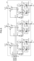
FIG. 1 is a diagram showing a configuration of a first embodiment according toClaim 1 of the present invention. -
FIG. 2 is a diagram showing a current regulator according toClaim 1 of the present invention. -
FIG. 3 is a diagram showing one of PWM modulations (unipolar modulation) of a 3-level converter. -
FIG. 4 is a diagram showing one of PWM modulations (dipolar modulation) of a 3-level converter. -
FIG. 5 is a diagram showing a mode switcher according toClaim 1 of the present invention. -
FIG. 6 is an operation waveform diagram when a close-end 3-phase ground fault occurs in the configuration according toClaim 1 of the present invention. -
FIG. 7 is an operation waveform diagram when 3-phase individual AC current control is excluded in the configuration according toClaim 1 of the present invention. -
FIG. 8 is an operation waveform diagram when a mode switcher is excluded in the configuration according toClaim 1 of the present invention. -
FIG. 9 is an operation waveform diagram when the mode switcher is activated in the configuration according toClaim 1 of the present invention. -
FIG. 10 is a diagram showing another mode switcher according toClaim 1 of the present invention. -
FIG. 11 is a diagram showing a timer circuit of the other mode switcher according toClaim 1 of the present invention. -
FIG. 12 is a diagram showing operation of an on-delay circuit used in the present invention. -
FIG. 13 is a diagram showing a configuration of a second example according toClaim 1 of the present invention. -
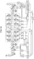
FIG. 14 is a diagram showing a configuration of a third example according toClaim 1 of the present invention. -
FIG. 15 is a diagram showing mode transition according toClaim 2 of the present invention. -
FIG. 16 is a diagram showing operation according toClaim 2 of the present invention. -
FIG. 17 is a diagram showing a configuration of an embodiment according toClaim 3 of the present invention. -
FIG. 18 is a diagram showing a mode switcher according to the embodiment according toClaim 3 of the present invention. -
FIG. 19 is a diagram showing a timer circuit according to the embodiment according toClaim 3 of the present invention. -
FIG. 20 is an operation waveform diagram when a close-end 3-phase ground fault occurs in the configuration according toClaim 3 of the present invention. -
FIG. 21 is an operation waveform diagram when the mode switcher is excluded in a fault with a close-end 1-phase ground fault open phase in the configuration according toClaim 3 of the present invention. -
FIG. 22 is an operation waveform diagram when the mode switcher is activated in a fault with a close-end 1-phase ground fault open phase in the configuration according toClaim 3 of the present invention. -
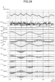
FIG. 23 is an operation waveform diagram when the mode switcher is excluded in the configuration according toClaim 3 of the present invention. -
FIG. 24 is an operation waveform diagram when the mode switcher is activated in the configuration according toClaim 3 of the present invention. -
FIG. 25 is a diagram showing a configuration of an embodiment according toClaim 4 of the present invention. -
FIG. 26 is a diagram showing a mode switching circuit of the embodiment according toClaim 4 of the present invention. -
FIG. 27 is a diagram showing a timer circuit of the embodiment according toClaim 4 of the present invention. -
FIG. 28 is a diagram showing operation according toClaims -
FIG. 29 is a diagram showing a timer circuit according toClaim 5 of the present invention. -
FIG. 30 is a diagram showing a timer circuit according toClaim 6 of the present invention. -
FIG. 31 is a diagram showing a configuration of a conventional FPC system. -
FIG. 32 is a diagram showing another configuration of the conventional FPC system. -
FIG. 33 is a diagram showing a configuration of an FPC system implemented by the present invention. -
FIG. 34 is a diagram showing a configuration of a conventional FPC system. -
FIG. 35 is a diagram showing a current regulator of the conventional FPC system. -
FIG. 36 is a diagram showing a gate pulse generator of a conventional 3-level converter. -
FIG. 37 is a diagram showing a mode switcher of a conventional mode 3-level converter. -
FIG. 38 is a diagram showing a charging period biased to a positive capacitor in a 3-level converter. -
FIG. 39 is a diagram showing a charging period biased to a negative capacitor in the 3-level converter. -
FIG. 40 is a mode diagram for distinguishing positive/negative capacitor voltage imbalance in a 3-level converter. - Hereinafter, embodiments of a 3-level converter and an adjustable speed generator motor system with full power converter (FPC system) according to the present invention will be described in detail with reference to the drawings. Note that the present invention is not limited by the embodiments.
- A system configuration of a first embodiment according to
Claim 1 of the present invention is described with reference toFIG. 1 . The descriptions of the same numbers as those described inFIG. 34 are the same and are omitted to avoid duplication. - The reference voltage phase signal (θe) 26 from the transformer-
side phase detector 25 is input to acurrent regulator 27 that controls the first 3-level converter 1. - The reactive power signal (Q_FB) 30 from the
power detector 29 and the external reactive power command (Q_REF) 31 are matched and input to thereactive power regulator 32. The direct-axis current command (ITD_REF) 33 is output from thereactive power regulator 32 and input to thecurrent regulator 27. - A signal (VC_DIF) 59 obtained by matching the DC voltage signal (VC_FB) 38 with the external DC voltage command (VC_REF) 39 is input to the
DC voltage regulator 40, and theDC voltage regulator 40 outputs the transvers-axis current command (ITQ_REF) 41 and inputs it to thecurrent regulator 27. The U-phase current (ITU) 42, the V-phase current (ITV) 43, and the W-phase current (ITW) 44 from the instrumentcurrent transformer 28 are input to thecurrent regulator 27. - The
current regulator 27 outputs a U-phase first mode command (M_TU1) 45, a V-phase first mode command (M_TV1) 46, and a W-phase first mode command (M_TW1) 47. - The rotation phase signal (θr) 50 from the
rotation phase detector 49 is input to acurrent regulator 51 that controls the second 3-level converter 8. - The reactive power signal (QM_FB) 55 from the
power detector 54 and the external reactive power command (QM_REF) 56 are matched and input to thereactive power regulator 57, and the direct-axis current command (IMD_REF) 58 from thereactive power regulator 57 is input to thecurrent regulator 51. - The match signal (VC_DIF) 59 of the DC voltage signal (VC_FB) 38 and the DC voltage command (VC_REF) 39 is input to a
dead band gain 60, and the input to an auxiliaryDC voltage regulator 61 is a value other than zero when the absolute value of deviation exceeds a threshold. The auxiliaryDC voltage regulator 61 outputs an active power command correction (ΔP_REF) 62, matches a correctionactive power command 64 energized to the external active power command (P_REF) 63 with the active power signal (P_FB) 65 from thepower detector 29, and inputs it to anactive power regulator 66. - Note that, the active power command correction (ΔP_REF) 62 energizes the correction
active power command 64 to the electricalrotating machine 21 in the power generation direction when the match signal (VC_DIF) 59 is positive and the DC voltage signal (VC_FB) 38 is lower than the DC voltage command (VC_REF) 39, and energizes the correctionactive power command 64 in the electric direction when the match signal (VC_DIF) 59 is negative. - The output signal of the
pulse generator 48 directly connected to the rotation shaft of the electricalrotating machine 21 is branched and input to aspeed detector 70, and a rotation speed signal (N_FB) 71 is output. - The auxiliary
DC voltage regulator 61 branches and outputs the active power command correction (ΔP_REF) 62, energizes it to an external speed command (N_REF) 72, matches it with acorrection speed command 73 and the rotation speed signal (N_FB) 71 from thespeed detector 70, and inputs it to aspeed regulator 74. - Note that, the active power command correction (ΔP_REF) 62 energizes the
correction speed command 73 to the electricalrotating machine 21 in the deceleration direction when the match signal (VC_DIF) 59 is positive and the DC voltage signal (VC_FB) 38 is lower than the DC voltage command (VC_REF) 39, and energizes thecorrection speed command 73 in the acceleration direction when the match signal (VC_DIF) 59 is negative. - An
output signal 67 of theactive power regulator 66 and anoutput signal 75 of thespeed regulator 74 are selectively output by amode selector switch 68, and a transvers-axis current command (IMQ_REF) 69 is output and input to thecurrent regulator 51. - The U-phase current (IMU) 76, the V-phase current (IMV) 77, and the W-phase current (IMW) 78 from the instrument
current transformer 53 are input to thecurrent regulator 51. - The
current regulator 51 outputs a mode command (M_MU) 79, a mode command (M_MV) 80, and a mode command (M_MW) 81. - The first mode commands 45, 46, and 47 are input to a
mode command switcher 82. The 3-phase current signals 42, 43, and 44 from the instrumentcurrent transformer 28 are input to themode command switcher 82 to calculate a second mode command, and a first mode command and a second mode command are selected to output a U-phase mode command (M_TU) 83, a V-phase mode command (M_TV) 84, and a W-phase mode command (M_TW) 85 to the first 3-level converter 1. The 3-phase mode commands 83, 84, and 85 are input togate pulse generators output gate pulses current regulator 51 to the second 3-level converter 8 are input togate pulse generators output gate pulses gate pulse generators - An embodiment of the
current regulator 27 of the first 3-level converter 1 is described with reference toFIG. 2 . Thecurrent regulator 51 of the second 3-level converter 8 has the same configuration as that of thecurrent regulator 27. Alternatively, it may have the same configuration as that of thecurrent regulator 3451 shown inFIG. 34 . The descriptions of the same numbers as those described inFIG. 35 are the same and are omitted to avoid duplication. - A 2-phase/3-phase calculator 235 receives the phase reference signal (θ) 201, the direct-axis current command (ID_REF) 208, and the transvers-axis current command (IQ_REF) 211, and outputs a U-phase current command (IU_REF) 236, a V-phase current command (IV_REF) 237, and a W-phase current command (IW_REF) 238.
- A U-phase AC
current regulator 239 matches and receives the U-phase current command (IU_REF) 236 and the U-phase current (IU) 202, and outputs a U-phase voltage command second stage (VU2_REF) 240. The configurations for the V phase and the W phase are the same as that for the U phase, and the descriptions of ACcurrent regulators second stages - Here, the AC
current regulators - An
output limiter 218 limits upper and lower limits of the signal obtained by energizing the U-phase voltage command first stage (VU1_REF) 215 and the U-phase voltage command second stage (VU2_REF) 240, and outputs a U-phase voltage command third stage (VU3_REF) 221. The configurations for the V phase and the W phase are the same as that for the U phase, and the descriptions ofoutput limiters third stages - An
overmodulation suppression circuit 224 inputs the voltage commandthird stages value selection circuit 225 and the minimum-value selection circuit 226, energizes outputs of the maximum-value selection circuit 225 and the minimum-value selection circuit 226, and outputs thevoltage correction command 228 through thegain 227. - A U-phase modulated-wave command (α_U) 229 is a signal obtained by subtracting the
voltage correction command 228 from the U-phase voltage command third stage (VU3_REF) 221. The U-phase modulated-wave command (α_U) 229 is input to a U-phase 3-level PWM modulator 230, and a U-phase mode command (M_U1) 231 is output. Modulated-wave commands 232 and 245, 3-level PWM modulators -
FIG. 3 is a diagram showing operation of the 3-level PWM modulator 230. The operation of a PWM modulator, which is generally called unipolar modulation, is shown. Hereinafter, the case for the U phase is described as an example. - When the value of the U-phase modulated-wave command (α_U) 229 is greater than a P-
side carrier wave 301, the U-phase mode command (M_U) 231 is output as level +1. When the value is smaller than an N-side carrier wave 302, the U-phase mode command (M_U) 231 is output as level -1. In other cases, the U-phase mode command (M_U) 231 is output aslevel 0. -
FIG. 4 is a diagram showing operation of another 3-level PWM modulator 230. The operation of a PWM modulator, which is generally called dipolar modulation, is shown. Hereinafter, the case for the U phase is described as an example. - The U-phase modulated-wave command (α_U) 229 is input to an
output regulator 401, and a modulated-wave correction command (β_U) 402 is output. When the value of the modulated-wave correction command 402 is greater than a P-side carrier wave 403, the U-phase mode command (M_U) 231 is output as level +1. When the value of the modulated-wave correction command 402 is smaller than an N-side carrier wave 404, the U-phase mode command (M_U) 231 is output as level -1. In other cases, the U-phase mode command (M_U) 231 is output aslevel 0. -
FIG. 5 is a diagram showing an embodiment of themode command switcher 82 shown inFIG. 1 . - The current signal (ITU) 42 from the instrument
current transformer 28 is input to a comparator withhysteresis 502. When the current signal (ITU) 42 exceeds a positive threshold I1 to the positive side, a signal (SW_TUN) 504 is switched fromlevel 0 tolevel 1. When the current signal (ITU) 42 falls below a positive threshold I2, which has a smaller absolute value than I1, the signal (SW_TUN) 504 is switched fromlevel 1 tolevel 0. At the same time, the current signal (ITU) 42 from the instrumentcurrent transformer 28 is input to a comparator withhysteresis 503. When the current signal (ITU) 42 exceeds a threshold -I1 to the negative side, a signal (SW_TUP) 505 is switched fromlevel 0 tolevel 1. When the current signal (ITU) 42 exceeds a negative threshold -12, which has a greater absolute value than -I1, the signal (SW_TUP) 505 is switched fromlevel 1 tolevel 0. - A
signal outputter 501 outputs a second mode command (M_TU2) 506 atlevel 1 when the signal (SW_TUP) 505 islevel 1, and outputs the second mode command (M_TU2) 506 at level -1 when the signal (SW_TUN) 504 islevel 1. - A signal (SW_TU) 507 is an OR output of (SW_TUN) 504 and (SW_TUP) 505, and the U-phase mode command (M_TW) 83 is selectively output by a
selector switch 508. Theselector switch 508 selectively outputs the U-phase first mode command (M_TU1) 45 when the signal (SW_TU) 507 islevel 0, and selectively outputs the U-phase second mode command (M_TU2) 506 when the signal (SW_TU) 507 islevel 1. - As shown in
FIG. 5 , themode command switcher 82 has a 3-phase independent configuration, the V phase and the W phase are the same as the U phase, and the descriptions thereof are omitted to avoid duplication. -
FIG. 6 is an operation waveform diagram when a close-end 3-phase ground fault occurs when the FPC system of the embodiment according toClaim 1 of the present invention shown inFIGS. 1 to 5 is connected to a double-circuit power line or when loop transmission is performed. - Hereinafter, the operation waveform diagrams of the embodiments of the present invention are unified to the dipolar modulation in
FIG. 4 as the PWM modulation. - Hereinafter, the measurement positions of the operation waveforms shown in
FIG. 6 are described with the numbers and reference signs shown inFIG. 1 . InFIG. 6 , six waveforms from the top are the voltages (phase voltages) and the currents of a system-side terminal 100 of theunit transformer 18 inFIG. 1 . - The seventh to twelfth waveforms from the top are the active power signal (P_FB) 65 and the reactive power signal (Q_FB) 30 of the
unit transformer 18 on the first 3-level converter 1 side, an active power signal (PM_FB) 101 and the reactive power signal (QM_FB) 55 of the electricalrotating machine 21, the positive capacitor voltage signal (VDCP) 36, and the negative capacitor voltage signal (VDCN) 37. The thirteenth active power command correction (ΔP_REF) 62 from the top is the output of the auxiliaryDC voltage regulator 61. - The fourteenth waveform from the top is the signal (SW_TU) 507 in
FIG. 5 . The signal (SW_TU) 507 inFIG. 5 selects the U-phase second mode command (M_TU2) 506 and becomeslevel 1 when outputting the U-phase mode command (M_Mu) 79. The fifteenth waveform from the top inFIG. 6 is a signal (SW_TV) 517 inFIG. 5 , and the sixteenth waveform is a signal (SW_TW) 527 inFIG. 5 . - In the above waveforms, a 3-phase ground fault occurs at time 0.2 [s] in
FIG. 6 . Since a ground fault occurs at the close end of theunit transformer 18, thephase voltage 100 becomes 0 for all the three phases. - During the close-end 3-phase ground fault period, the active power cannot be output to the transmission side, and the active power signal (P_FB) 65 becomes zero. Since the active power signal (PM_FB) 101 of the electrical
rotating machine 21 follows the active power command (P_REF) 63, the active power from the electricalrotating machine 21 to the second 3-level converter 8 is stored in the positive capacitor (CBP) 15 and the negative capacitor (CBN) 16, and the positive capacitor voltage signal (VDCP) 36 and the negative capacitor voltage signal (VDCN) 37 rise sharply to 1.2 times their ratings. - Here, the capacitance of the positive capacitor (CBP) 15 and the negative capacitor (CBN) 16 is downsized to the limit to keep the direct-axis
current controller 209 and the transvers-axiscurrent controller 212 stable. - In
FIG. 6 , the system-side circuit breaker operates in four cycles after the 3-phase ground fault occurs to remove the fault phase, and the remaining one-line transmission is performed. - In the embodiment of the present invention, when the capacitor voltage signal (VC_DIF) 59, which is the deviation between the DC voltage signal (VC_FB) 38 and the DC voltage command (VC_REF) 39, exceeds the threshold of the
dead band gain 60, the active power command correction (ΔP_REF) 62 rises to 1 PU in the electric motor direction by the auxiliaryDC voltage regulator 61 to suppress the rise of the positive capacitor voltage signal (VDCP) 36 and the negative capacitor voltage signal (VDCN) 37 to return to the set value, and the active power command correction (ΔP_REF) 62 returns to zero. Thus, the active power signal (P_FB) 65 can also be brought close to the level before the close-end 3-phase ground fault. - The signal (SW_TU) 507, the signal (SW_TV) 517, and the signal (SW_TW) 527 intermittently become
level 1 independently for three phases after the ground fault occurs, but the period in which the second mode command is selectively output by themode command switcher 82 ends within two cycles after the fault phase is removed. - In a conventional FPC system, it has been necessary to wait nearly one second for the active power signal (P_FB) 65 to return. Since the decrease in the active power until the return is the acceleration power of the wind turbine or the hydraulic turbine, a significant increase in the rotational speed of the electrical
rotating machine 21 could not be avoided. In order to avoid this increase in the rotational speed, the positive discharge resistance (RP) 3401 and the negative discharge resistance (RN) 3402 inFIG. 34 have been treated mostly as Joule heat. - In addition, the positive capacitor voltage signal (VDCP) 36 and the negative capacitor voltage signal (VDCN) 37 rise up to 1.2 times, but which is limited only during the ground fault period. Therefore, by appropriately selecting a capacitor, the influence on the reliability and lifetime of the capacitor can be avoided.
- As described above, the embodiment of the present invention has an effect of implementing the FPC system capable of continuing operation even in the event of a close-end 3-phase ground fault without using a discharge resistance.
-
FIG. 7 is a diagram showing operation waveforms when the ACcurrent regulators FIG. 2 are excluded under the same conditions as inFIG. 6 in order to evaluate the effect of the AC current regulators. The measurement positions are the same as those inFIG. 6 . When the AC current regulators are removed in the same configuration as inFIG. 6 , the direct-axiscurrent controller 209 and the transvers-axiscurrent controller 212 become unstable. Then, the DC voltage signal (VC_FB) 38 exceeds twice the value before the ground fault, and the DC voltage command (VC_REF) 39 securing the economic efficiency cannot protect the positive capacitor (CBP) 15 and the negative capacitor (CBN) 16, and the operation cannot be continued. - In the following,
FIG. 7 shows operation waveforms when the capacitor capacitance is doubled as compared with the case inFIG. 6 . Due to this influence, the voltage increase rate of the positive capacitor voltage signal (VDCP) 36 and the negative capacitor voltage signal (VDCN) 37 immediately after the 3-phase ground fault at time 0.2 [s] is reduced to 1/2 as compared with the case inFIG. 6 . - When the AC current regulators are removed, it is necessary to increase the capacitor capacitance of the positive capacitor (CBP) 15 and the negative capacitor (CBN) 16 to about 2 times in order to keep the direct-axis
current controller 209 and the transvers-axiscurrent controller 212 stable in the event of a symmetrical fault such as a 3-phase ground fault and to increase the capacitor capacitance to about 4 times in the event of an asymmetrical fault. This indicates a capacitor capacitance reduction effect of the AC current regulators. -
FIGS. 8 and9 are operation waveform diagrams for evaluating an overcurrent suppression effect.FIG. 8 shows a case in which themode command switcher 82 is excluded, andFIG. 9 shows a case in which the operation is performed. - In the following, the measurement positions of the operation waveforms shown in
FIG. 8 are described with the numbers and reference signs shown inFIGS. 5 and1 . - In the two waveforms from the top, the U-phase mode command (M_TU) 83 of the first 3-
level converter 1 is switched to level +1 when the signal (SW_TUP) 505 inFIG. 5 islevel 1. When the signal (SW_TUN) 504 islevel 1, the U-phase mode command (M_TU) 83 is switched to level -1. In the case inFIG. 8 , since themode command switcher 82 is excluded, the level is 0. - Next, the third waveform from the top is the U-phase mode command (M_TU) 83 of the first 3-
level converter 1 inFIG. 1 . - The
reference sign 42 is the U-phase current (ITU), and the positive side indicates the current in the outflow direction from the U-phase terminal of the first 3-level converter 1. - A
reference sign 102 is a U-phase P element current (I_TUP) of the first 3-level converter 1; the positive side indicates the current value of the electronic switch, and the negative side indicates the current value of the FWD. - A
reference sign 103 is a U-phase PC element current (I_TUPC) of the first 3-level converter 1; the positive side indicates the current value of the electronic switch, and the negative side indicates the current value of the FWD. -
Reference sign 104 is a U-phase P-side clamp diode current (I_TCUP) of the first 3-level converter 1, and a negative side indicates a current value of the diode. - A
reference sign 105 is a U-phase N element current (I_TUN) of the first 3-level converter 1; the positive side indicates the current value of the electronic switch, and the negative side indicates the current value of the FWD. - A
reference sign 106 is a U-phase NC element current (I_TUNC) of the first 3-level converter 1; the positive side indicates the current value of the electronic switch, and the negative side indicates the current value of the FWD. - A
reference sign 107 is a U-phase N-side clamp diode current (I_TCUN) of the first 3-level converter 1, and a negative side indicates the current value of the diode. - In
FIG. 8 , the impedance of theunit transformer 18 and aharmonic filter 28 is adjusted so that the current in the event of a fault is twice the current value in the steady state before the ground fault occurs at time 0.2 [s], in accordance with the design of a conventional standard 3-level converter. -
FIG. 9 shows when themode command switcher 82 is operating. In the following, the measurement positions of the operation waveforms shown inFIG. 9 are the same as those inFIG. 8 , and the descriptions thereof are omitted to avoid duplication. - After a 3-phase ground fault occurs at time 0.2 [s], the signal (SW_TUP) 505 changes to
level 1 twice by time 0.205 seconds. In the embodiment inFIG. 9 , the threshold (I1) of the comparators withhysteresis signal 505 rises tolevel 1, the U-phase current (ITU) is switched from the electronic switches of the N element and the NC element to the FWDs of the P element and the PC element, and the maximum current of the U-phase current (ITU) is reduced to 1.25 times from 2 times inFIG. 8 . In addition, the signal (SW_TUN) 504 changes tolevel 1 three times in a period from time 0.210 [s] to time 0.205 [s]. - When the
signal 504 rises tolevel 1, the U-phase current (ITU) is switched from the electronic switches of the P element and the PC element to the FWDs of the N element and the NC element, and the maximum current of the U-phase current (ITU) is reduced to 1.25 times from 2 times inFIG. 8 . - In the embodiment in
FIG. 9 , the threshold (I2) of the comparators withhysteresis signal 504 and thesignal 505 is long, and the number of times of rising can be reduced. As a result, there is an effect of reducing the number of switching operations during a system fault and reducing the switching loss of the electronic switches and the FWDs. In addition, since themode command switcher 82 reduces the overcurrent level by 35% from 2 times to 1.25 times the steady state, there is an effect of reducing the conduction loss of the electronic switches and the FWDs. - Another embodiment of the
mode command switcher 82 is described with reference toFIG. 10 . - The current signal (ITU) 42 from the instrument
current transformer 28 is input to acomparator 1002,level 1 is output as a signal (SW_TUN) 1004 when the current signal (ITU) 42 exceeds the positive threshold I1 to the positive side, andlevel 0 is output when the current signal (ITU) 42 falls below the positive threshold I1. At the same time, the current signal (ITU) 42 from the instrumentcurrent transformer 28 is input to acomparator 1003,level 1 is output as a signal (SW_TUP) 1005 when the current signal (ITU) 42 exceeds the threshold -I1 to the negative side, andlevel 0 is output when the current signal (ITU) 42 falls below the threshold -I1. - A
timer circuit 1006 receives the signal (SW_TUP) 1005 and the signal (SW_TUN) 1004 and outputs a U-phase second mode command (M_TU2) 1007 and a signal (SW_TU) 1008. - A
selector switch 1009 selectively outputs the U-phase first mode command (M_TU1) 45 when the signal (SW_TU) 1008 islevel 0, and the U-phase second mode command (M_TU2) 1007 when the signal (SW_TU) 1008 islevel 1 as the U-phase mode command (M_TU) 83. - As shown in
FIG. 10 , themode command switcher 82 has a 3-phase independent configuration, the V phase and the W phase are the same as the U phase, and the descriptions thereof are omitted to avoid duplication. - An embodiment of the
timer circuit 1006 is described with reference toFIG. 11 . - The signal (SW_TUP) 1005 is input to the set side of a flip-flop circuit with
reset priority 1102, and an output signal (X) 1103 is input to an on-delay circuit 1104. An output signal (Y) 1105 of the on-delay circuit 1104 is input to the reset side of the flip-flop circuit 1102. Similarly, the signal (SW_TUN) 1004 is input to the set side of a flip-flop circuit withreset priority 1106, and anoutput signal 1107 is input to an on-delay circuit 1108. Anoutput signal 1109 of the on-delay circuit 1108 is input to the reset side of the flip-flop circuit 1106. - A
signal outputter 1110 outputslevel 1 as the second mode command (M_TU2) 1007 when thesignal 1103 islevel 1, and outputs level -1 as the second mode command (M_TU2) 1007 when thesignal 1107 islevel 1. The signal (SW_TU) 1008 is an OR output of thesignal 1103 and thesignal 1107. - In the above, the on-
delay circuits - An example of the on-
delay circuit 1104 is described with reference toFIG. 12 . - When the input signal (X) 1103 changes from
level 0 tolevel 1 and then maintainslevel 1 for more than a delay set time Td, the output signal (Y) 1105 changes fromlevel 0 tolevel 1. When the input signal (X) 1103 changes fromlevel 1 tolevel 0, the output signal (Y) 1105 changes fromlevel 1 tolevel 0. - According to the embodiment in
FIGS. 10 to 12 , of themode command switcher 82, the range of the signal 1004 (SW_TUN), the signal 1005 (SW_TUP), the signal 1014 (SW_TVN), the signal 1015 (SW_TVP), the signal 1024 (SW_TWN), the signal 1025 (SW_TWP), the U-phase mode command (M_TU) 83, the V-phase mode command (M_TV) 84, and the W-phase mode command (M_TW) 85 can be achieved only by the 2-level signal logical circuit and timer circuit, and there is an effect that the range can be achieved without being limited by the calculation cycle of a microprocessor. Therefore, it is possible to implement the first 3-level converter 1 suitable for small-capacity applications in which a high PWM frequency is often selected to downsize the system. - A system configuration according to a second embodiment according to
Claim 1 of the present invention is described with reference toFIG. 13 . The descriptions of the same numbers as those described inFIG. 1 are the same and are omitted to avoid duplication. - An
active power regulator 1366 matches and receives an active power signal (PM_FB) 1301 from thepower detector 54 provided on the electricalrotating machine 21 side and the correctionactive power command 64, and outputs a signal 1367. A mode selector switch 1368 selectively outputs the output signal 1367 of theactive power regulator 1366 and theoutput signal 75 of thespeed regulator 74, and inputs the signal to thecurrent regulator 51 as a transvers-axis current command (IMQ_REF) 1369. - According to the embodiment in
FIG. 13 , since the external active power command (P_REF) 64 and the active power signal (PM_FB) 1301 are matched and input to theactive power regulator 1366, there is an effect of quickly recovering after fault phase removal and minimizing the increase in rotation speed of the electricalrotating machine 21. - A system configuration according to a third embodiment according to
Claim 1 of the present invention is described with reference toFIG. 14 . The descriptions of the same numbers as those described inFIG. 1 are the same and are omitted to avoid duplication. - An active power regulator 1466 receives the active power signal (P_FB) 65 from the
power detector 29 and the external active power command 63 (P_REF) that have been matched, and outputs asignal 1467. A speed regulator 1474 receives the rotational speed signal (N_FB) 71 from thespeed detector 70 and the external speed command (N_REF) 72 that have been matched, and outputs asignal 1475. - A
mode selector switch 1468 selectively outputs theoutput signal 1467 of the active power regulator 1466 and theoutput signal 1475 of the speed regulator 1474 as asignal 1469. - The match signal (VC_DIF) 59 of the DC voltage signal (VC_FB) 38 and the DC voltage command (VC_REF) 39 is input to a
dead band gain 1460, and the input to an auxiliaryDC voltage regulator 1461 is a value other than zero when the absolute value of deviation exceeds a threshold. The auxiliaryDC voltage regulator 1461 outputs a transvers-axis current command correction (ΔIMQ_REF) 1462, energizes it to thesignal 1469 from themode selector switch 1468, and inputs it to thecurrent regulator 51 as a transvers-axis current command (IMQ_REF) 1470. The transvers-axis current command correction (ΔIMQ_REF) 1462 energizes the transvers-axis current command (IMQ_REF) 1470 to the electricalrotating machine 21 in the power generation direction when the match signal (VC_DIF) 59 is positive and the DC voltage signal (VC_FB) 38 is lower than the DC voltage command (VC_REF) 39, and energizes the transvers-axis current command (IMQ_REF) 1470 in the electric direction when the match signal (VC_DIF) 59 is negative. - According to the embodiment in
FIG. 14 , since the transvers-axis current command (IMQ_REF) 1470 obtained by energizing the transvers-axis current command correction (ΔIMQ_REF) 1462 to thesignal 1469 from themode selector switch 1468 is directly input to thecurrent regulator 51, there is an effect of suppressing and recovering the capacitor voltage signal (VC_DIF) 59 at a high speed particularly when the speed regulator 1474 is used. - An embodiment according to
Claim 2 of the present invention is described with reference toFIGS. 15 and16 . -
FIG. 15 shows the state transition of a mode command (M) 1511, which is one input to thegate pulse generators - A
reference sign 1516 indicates a four-output gate pulse state in a mode command (M=0) state, areference sign 1517 indicates a four-output gate pulse state in a mode command (M=+1) state, and areference sign 1518 indicates a four-output gate pulse state in a mode command (M=-1) state. - In the present invention, in order to secure the dead time compensation period of the first 3-
level converter 1, a dead time compensation circuit is provided in thegate pulse generators mode command switcher 82 to prevent a short circuit. - In the following, an operation in a normal operation state is described.
- The dead time compensation period of the first 3-
level converter 1 is provided during the transition between the mode command (M=0)state 1516 and the mode command (M=+1)state 1517. - For the sake of explanation, the mode during the dead time period is referred to as a (M=+1_D) 1519 state. In addition, a dead time period of the first 3-level converter is provided during the transition between the mode command (M=0)
state 1516 and the mode command (M=-1)state 1518. For the sake of explanation, the mode during the dead time period is referred to as a (M=-1_D) 1520 state. The transitions between the above states are denoted by 1501, 1502, 1503, 1504, 1505, 1506, 1507, and 1508. -
FIG. 16 is a waveform diagram showing waveforms of the respective components with the dead time period expanded. - From the top in
FIG. 16 , a mode command (M) 1601, a gate pulse (G_P) 1602 to the P element, a gate current (IG_P) 1603 of the P element, a current (I_P) 1604 of the P element, a gate pulse (G_PC) 1605 of the PC element, a gate current (IG_PC) 1606 of the PC element, a current (I_PC) 1607 of the PC element, a P-side clamp diode current (I_CP) 1608, a gate pulse (G_N) 1609 to the N element, a gate current (IG_N) 1610 of the N element, a PC current (I_N) 1611 of the N element, a gate pulse (G_PC) 1612 of the NC element, a gate current (IG_NC) 1613 of the NC element, a current (I_NC) 1614 of the NC element, and an N-side clamp diode current (I_CN) 1615 are shown. - Here, the four
element currents clamp diode currents 1608 and 1615 indicate the currents in the negative direction. The fourgate currents - The
gate transition 1501 inFIG. 15 occurs when the mode command (M) 1601 changes fromlevel 0 tolevel 1 at time (t1p) 1531 inFIG. 16 , and thetransition 1502 occurs attime 1532 after a dead time set period Td1. Similarly, the gate transitions 1503 to 1508 also occur from time (t2p) 1533 totime 1538 inFIG. 16 . - The above is the operation of the dead time compensation circuit provided in the
gate pulse generators - Next, an operation when the current detection value exceeds the threshold I1 at the
mode command switcher 82 according toClaim 1 of the present invention is described. - In the first 3-
level converter 1 of the present invention, a dead time compensation period Td2 is provided during the transition between the mode command (M=+1)state 1517 and the mode command (M=-1)state 1518. For the sake of explanation, the mode during the dead time period is referred to as a (M=0_D) 1521 state. The dead time compensation period Td2 in the 1521 state is set to be longer than the dead time set period Td1 of 1519 and 1520. - In the following, the operation when the current detection value exceeds the threshold I1 at time (t6 p) 1539 is described with reference to
FIG. 16 . - The state immediately before time (t6 p) 1539 is the same as the state immediately before the previous time (t2 p) 1533, and the description thereof is omitted to avoid duplication.
- A
state transition 1509 inFIG. 15 occurs at time (t6 p) 1539.FIG. 16 shows a state in which the current (I_P) 1604 of the element P is positive and the electronic switch conducts a current. When the mode command (M) 1601 changes from (M=+1) to (M=-1) in this state, the gate pulse (G_P) 1602 to the P element and the gate pulse (G_PC) 1605 of the PC element change from ON to OFF, and both the electronic switches of the P element and the PC element start turn-off. - The turn-off time from the off-change of the gate pulse to the element-off state becomes longer as the current value at the start of turn-off becomes larger. Therefore, since the turn-off is at time (t6p) 1539 when the current detection value exceeds the threshold I1, both of a turn-off time (T_p) 1616 of the P element and a turn-off time (T_CP) 1617 of the PC element become longer than the turn-off time during the normal operation. Therefore, in terms of preventing a short circuit, it is desirable to set the dead time compensation period Td2 longer than usual. On the other hand, if the setting of the dead time compensation period Td2 is too long, there is a side effect such as loss of controllability.
- At
time 1540 after the dead time compensation period Td2 from time (t6 p) 1539, the gate pulse (G_N) 1609 to the N element and the gate pulse (G_PC) 1612 to the NC element change to ON, but in the arm, the FWD has already started conducting a current at time (t6 p) 1539, and no current/voltage change occurs in both the N element and the NC element. As a result, even if the dead time compensation period Td2 is set to be longer, no adverse effect occurs. - The adverse effect can occur when the P element current (I_P) is negative and the FWD conducts a current at the time when the mode command (M) 1601 changes from (M=+1) to (M=-1) as at time (t6 n) 1618 in
FIG. 16 . - In this case, since the N element (I_N) 1611 and the NC element (I_NC) 1614 start turn-on at
time 1619 after the dead time compensation period Td2 from time (t6n) 1618 inFIG. 16 , an influence of setting the dead time compensation period Td2 to be longer appears. However, since themode command switcher 82 of the present invention detects the sign of the element current and performs the mode switching, the phenomena at time (t6 n) 1618 andtime 1619 inFIG. 16 are suppressed. - From the above, by setting the dead time compensation period Td2 longer than a normal dead time compensation period Td1, it is possible to suppress adverse effects due to the turn-on delay while preventing a short circuit.
- A system configuration of a first embodiment according to
Claim 3 of the present invention is described with reference toFIG. 17 . The descriptions of the same numbers as those described inFIG. 1 are the same and are omitted to avoid duplication. - The U-phase current (IMU) 76, the V-phase current (IMV) 77, and the W-phase current (IMW) 78 from the instrument
current transformer 53 are input to acurrent regulator 1701. Thecurrent regulator 1701 outputs a U-phase first mode command (M_MU1) 1779, a V-phase first mode command (M_MV1) 1780, and a W-phase first mode command (M _MW1) 1781 to amode command switcher 1702. Here, the configuration of thecurrent regulator 1701 may be the same as that of thecurrent regulator 51 inFIG. 1 . - The direct-axis current command (IMD_REF) 58 from the
reactive power regulator 57 is branched and output, and is input to themode command switcher 1702 and a 2-phase/3-phase converter 1703. In addition, the transvers-axis current command (IMQ_REF) 69 from themode selector switch 68 is branched and output, and is input to themode command switcher 1702 and the 2-phase/3-phase converter 1703. - The 2-phase/3-
phase converter 1703 receives the rotation phase signal (θr) 50, outputs a U-phase current command (IMU_REF) 1704, a V-phase current command (IMV_REF) 1705, and a W-phase current command (IMW_REF) 1706, and inputs them to themode command switcher 1702. The voltage signal (VDCP) 36 of the positive capacitor (CBP) 15 and the voltage signal (VDCN) 37 of the negative capacitor (CBN) 16 are input to themode command switcher 1702. - The
mode command switcher 1702 receives the above 10 signals, and outputs, togate pulse generators 1789, 1790, and 1791, a U-phase mode command (M_MU) 1707, a V-phase mode command (M_MV) 1708, and a W-phase mode command (M_MW) 1709 to the second 3-level converter 8. Thegate pulse generators 1789, 1790, and 1791 each output 4-output gate pulses level converter 8. Here, thegate pulse generators 1789, 1790, and 1791 each include a dead time compensation circuit that delays the rise of the gate pulse for the purpose of preventing circuit shorts. - An embodiment of the
mode command switcher 1702 is described with reference toFIG. 18 . - The voltage signal (VDCP) 36 of the positive capacitor (CBP) 15 and the voltage signal (VDCN) 37 of the negative capacitor (CBN) 16 are matched to calculate a difference voltage (VC_DIF) 1801, and the difference voltage (VC_DIF) 1801 is input to a comparator with
hysteresis 1804. The comparator withhysteresis 1804 switches a signal (SW_VCN) 1805 fromlevel 0 tolevel 1 when the difference voltage (VC_DIF) 1801 exceeds a positive threshold V1 to the positive side, and switches the signal (SW_VCN) 1805 fromlevel 1 tolevel 0 when the difference voltage (VC_DIF) 1801 falls below a positive threshold V2 having an absolute value smaller than V1. In addition, the difference voltage (VC_DIF) 1801 is input to a comparator withhysteresis 1802, and the comparator withhysteresis 1802 switches a signal (SW_VCP) 1803 fromlevel 0 tolevel 1 when the difference voltage (VC_DIF) 1801 falls below a negative threshold -V1 to the negative side, and switches the signal (SW_VCP) 1803 fromlevel 1 tolevel 0 when the difference voltage (VC_DIF) 1801 exceeds a threshold -V2. - A root-
square sum calculator 1806 inputs a root-squaresum output signal 1807 of the direct-axis current command (IMD_REF) 58 and the transvers-axis current command (IMQ_REF) 69 to the denominator side of adivider 1808. The U-phase current command (IMU_REF) 1704 is input to the numerator side of thedivider 1808, and thedivider 1808 outputs a U-phasecurrent command signal 1809 in which the amplitude of the 3-phase current command is unitized. - A
comparator 1811outputs level 1 when the unitized U-phasecurrent command signal 1809 exceeds a positive threshold C1 to the positive side, and outputslevel 0 in other cases. Acomparator 1810outputs level 1 when the unitized U-phasecurrent command signal 1809 falls below a negative threshold -C1 to the negative side, and outputslevel 0 in other cases. Here, the value of the threshold C1 is set to a value between 0.86 and 1.0. - A signal (SW_MUP) 1812 is a logical conjunction of the output of the
comparator 1810 and the signal (SW_VCP) 1803, and a signal (SW_MUN) 1813 is a logical conjunction of the output of thecomparator 1811 and the signal (SW_VCN) 1805. - A
timer circuit 1814 receives the signal (SW_MUP) 1812 and the signal (SW_MUN) 1813, and outputs a second mode command (M_MU2) 1815 and a signal (SW_MU) 1816. - A
selector switch 1817 selects the first mode command (M_MU1) 1779 when the signal (SW_MU) 1816 islevel 0 and selects the second mode command (M_MU2) 1815 when the signal (SW_MU) 1816 islevel 1, and outputs the mode command (M_MU) 1707. - As shown in
FIG. 18 , the configurations and operations for the V phase and the W phase are similar, and the descriptions thereof are omitted to avoid duplication. - An embodiment of the
timer circuit 1814 is described with reference toFIG. 19 . - When a
signal 1901 islevel 1,level 0 is output as the second mode command (M_2) 1815. When the input signal (SW_P) 1812 changes fromlevel 0 tolevel 1 in a state where thesignal 1901 islevel 0, asignal 1902 also changes fromlevel 0 tolevel 1, andlevel 1 is output as the second mode command (M_2) 1815. - The change from
level 1 tolevel 0 of the input signal (SW_P) 1812 is detected using a previous-value holding circuit 1904, thesignal 1902 changes fromlevel 0 tolevel 1, and the second mode command (M_2) 1815 changes tolevel 0 since thesignal 1901 is the output of a flip-flop withreset priority 1909. At the same time, the timer of an on-delay circuit 1910 is started, and the flip-flop 1909 is reset tolevel 0 after the set time. - When the signal (SW_P) 1812 is
level 1 at the time when the flip-flop 1909 is reset, the second mode command (M_2) 1815 is set tolevel 1 again. - When the signal (SW_N) 1813 is
level 1 at the time when the flip-flop 1909 is reset, the second mode command (M_2) 1815 is set to level -1. - When the signal (SW_P) 1812 and the signal (SW_N) 1813 are both
level 0 at the time when the flip-flop 1909 is reset, the signal (SW) 1816 returns fromlevel 1 tolevel 0. -
FIG. 20 is an operation waveform diagram when a close-end 3-phase ground fault occurs when the FPC system of the embodiment according toClaim 3 of the present invention shown inFIGS. 17 to 19 is connected to a double-circuit power line or when loop transmission is performed. The configuration and control of the first 3-level converter 1, and the capacitance of the positive capacitor (CBP) 15 and the negative capacitor (CBN) 16 are the same as those inFIG. 6 , and the difference is that themode command switcher 1702 is additionally operated. - In the following, the measurement positions of the operation waveforms shown in
FIG. 20 are described with the numbers and reference signs shown inFIG. 17 . The descriptions of the same numbers as those described inFIG. 6 are the same. The descriptions thereof are omitted to avoid duplication. - The signal (SW_MU) 1816 becomes
level 1 when the U-phase mode command (M_MU) 1707 inFIG. 17 selectively outputs the second mode command (M_MU2) 1815 for capacitor voltage imbalance suppression. A reference sign 1826 (SW_MV) indicates the V phase, and a reference sign 1836 (SW_MW) indicates the W phase. - Compared to
FIG. 6 with the above operation waveforms, the voltage imbalance suppression operation by themode command switcher 1702 is sporadically performed on the system side before the 3-phase ground fault occurs at time 0.2 [s]. Since the 3-phase ground fault at time 0.2 [s] is a symmetrical fault, the signals (SW_MU) 1816, 1826 (SW_MV), and 1836 (SW_MW) alternate at approximately the same frequency, but the operation is completed within three cycles after the fault phase is removed, and the imbalance between the positive capacitor voltage signal (VDCP) 36 and the negative capacitor voltage signal (VDCN) 37 seen inFIG. 6 converges. - In the embodiment in
FIG. 20 , the threshold (V1) of the comparators withhysteresis - According to the embodiment in
FIG. 20 , there is an effect of maintaining the positive and negative capacitor voltage balance during steady operation without affecting normal control performance. -
FIGS. 21 and22 are operation waveform diagrams when a single line-to-ground fault on a single-circuit power line described inFIG. 33 to confirm the effect with and without themode command switcher 1702.FIG. 21 shows a case in which themode command switcher 1702 is excluded, andFIG. 22 shows a case in which themode command switcher 1702 is operated. - In the following, an A-phase single line-to-ground fault occurs at time t1=0.2 [s]. At time t2 after four cycles, the A-phase leading-end circuit breaker (52F_A) and the trailing-end circuit breaker (52B_A) are opened.
- Between time t1 and time t2, the A-phase voltage of the system-
side terminal 100 of theunit transformer 18 becomes zero because of a close-end fault. The leading-end circuit breaker (52F_A) is closed at time t3=1.1 [s], and subsequently the trailing-end circuit breaker (52B_A) is closed at time t4=1.25 [s]. As a result, the period from time t2 to time t4 is an open-phase period, and the A-phase current of the system-side terminal 100 of theunit transformer 18 becomes zero. Although the current of the first 3-level converter 1 is imbalanced during the open-phase period, there is an effect that the W-phase overcurrent is suppressed by amode switcher 82 and that the operation is continued, as shown by the waveform of the signal (SW_TU) 527. - When the trailing-end circuit breaker (52B_A) is closed at time t4, the U-phase signal (SW_TU) 507 and the V-phase signal (SW_TV) 517 also operate, but converge within two cycles. However, imbalance between the positive capacitor voltage signal (VDCP) 36 and the negative capacitor voltage signal (VDCN) 37 diverges after time t4.
-
FIG. 22 is an operation waveform diagram when themode command switcher 1702 is operated. - The imbalance between the positive capacitor voltage signal (VDCP) 36 and the negative capacitor voltage signal (VDCN) 37 seen after time t4 in
FIG. 21 converges due to the effect of themode command switcher 1702. Due to an asymmetrical fault, the number of times of operation of the U-phase signal (SW_MU) 1816 is the largest during the open-phase period, and the V-phase signal (SW_MV) 1826 is never operated. After the trailing-end circuit breaker (52B_A) is closed, the three phases operate together, but converge after 0.3 [s] from time t4. - The above is the difference, but the operation waveforms of the other parts are almost the same. This indicates that there is no side effect of the
mode command switcher 1702. - According to the embodiment in
FIG. 22 , there is an effect that themode command switcher 82 for overcurrent suppression provided on the first 3-level converter 1 side and themode command switcher 1702 for voltage imbalance suppression provided on the second 3-level converter 8 side operate without mutual interference and that stable operation is continued even in the event of a system-side asymmetrical fault including an open-phase period that is the weakest point of conventional frequency converters. -
FIGS. 23 and24 are comparative diagrams for showing the operation of amode switcher 1702 for voltage imbalance suppression when a close-end 3-phase ground fault occurs.FIG. 23 shows a case in which themode switcher 1702 is excluded, andFIG. 24 shows a case in which themode switcher 1702 is operated.FIG. 23 shows the detailed operation of the U-phase of the second 3-level converter 8 corresponding toFIG. 6 .FIG. 24 shows the detailed operation of the U-phase of the second 3-level converter 8 corresponding toFIG. 20 . - In the following, the measurement positions of the operation waveforms shown in
FIG. 23 are described with the numbers and reference signs shown inFIGS. 1 and18 . - From the top, a waveform 59 (VDCP-VDCN) is (VDC_DIF) 59 in
FIG. 1 and indicates a value obtained by subtracting the negative capacitor voltage from the positive capacitor voltage. - The next waveform (ICP-ICN) 2301 indicates a value obtained by subtracting the charging current of the negative capacitor (CBN) 16 from the charging current of the positive capacitor (CBP) 15, and is a waveform proportional to the time derivative of the
waveform 59. - The next waveform (SW_VCP) 1803 is the output of the comparator with
hysteresis 1802 inFIG. 18 , and becomeslevel 1 when the waveform 59 (VDCP-VDCN) exceeds the threshold (-V1) in the negative direction. - The next waveform (SW_VCN) 1803 becomes
level 1 when the waveform 59 (VDCP-VDCN) exceeds the threshold (V1) in the positive direction. - In the embodiment in
FIG. 23 , in order to substantially exclude themode switcher 1702, the threshold V1 is set to a large value to maintainlevel 0. - The next waveform (IMU_REF) 1704 is the U-phase current command (IMU_REF) 1704 of the second 3-
level converter 8 inFIG. 17 , and is the U-phase current command of the electricalrotating machine 21. - The next waveform (SW_MUP) 1812 is the signal (SW_MUP) 1812 in
FIG. 18 , and when this signal islevel 1, the U-phase mode command (M_MU) 1707 outputs level +1 by themode switcher 1702. - The next waveform (SW_MUN) 1813 is the signal (SW_MUN) 1813 in
FIG. 18 , and when this signal islevel 1, the U-phase mode command (M_MU) 1707 outputs level -1 by themode switcher 1702. - The next waveform (M_MU) 1707 is the 3-level U-phase mode command (M_MU) 1707 output to the U-phase gate pulse generator 1789.
- The next waveform (IMU) 76 is the U-phase current (IMU) 76 from the instrument
current transformer 53 inFIG. 1 , and the positive side indicates the current in the outflow direction from the U-phase terminal of second 3-level converter 8. - The
current regulator 1701 performs control to follow the U-phase current command (IMU_REF) 1704. - The next waveform (I_MUP) 108 is the current (I_MUP) of the U-phase P element of the second 3-
level converter 8; the positive side indicates the current value of the electronic switch, and the negative side indicates the current value of the FWD. - The next waveform (I_MUPC) 109 is the current (I _MUPC) of the U-phase PC element of the second 3-
level converter 8; the positive side indicates the current value of the electronic switch, and the negative side indicates the current value of the FWD. - The next waveform (I_MCUP) 110 is the U-phase P-side clamp diode current (I_MCUP) of the second 3-
level converter 8, and the negative side indicates the current value of the diode. - The next waveform (I_MUN) 111 is the current (I_MUN) of the U-phase N element of the second 3-
level converter 8; the positive side indicates the current value of the electronic switch, and the negative side indicates the current value of the FWD. - The next waveform (I_MUNC) 112 is the current (I_MUNC) of the U-phase NC element of the second 3-
level converter 8; the positive side indicates the current value of the electronic switch, and the negative side indicates the current value of the FWD. - The next waveform (I_MCUN) 113 is the U-phase N-side clamp diode current (I_MCUN) of the first 3-
level converter 1, and the negative side indicates the current value of the diode. - In the operation waveforms in
FIG. 23 described above, when the close-end triple line-to-ground fault occurs at time 0.2 [s], the amplitude of the U-phase mode command (M_MU) 1707 becomes a small value in order to suppress the positive and negative capacitor voltages, and the U-phase current (IMU) 76 also becomes a small value. However, almost no change is observed in the change pattern of the U-phase mode command (M_MU) 1707 before and after the close-end triple line-to-ground fault occurs, and as a result, no change other than the amplitude change is observed in thewaveforms 108 to 113. - The measurement positions of the operation waveforms shown in
FIG. 24 are the same as those inFIG. 23 , and the descriptions thereof are omitted to avoid duplication. - In the embodiment in
FIG. 24 , in order to operate themode switcher 1702, the threshold V1 is set to 1% similarly toFIGS. 20 and22 . - In
FIG. 24 , the waveform (SW_VCP) 1803 becomeslevel 1 once between time t=0.205 [s] to time t=0.21 [s] and from time t=0.214 [s] to time t=0.227 [s], and the negative capacitor voltage (VDCN) becomes larger than the positive capacitor voltage (VDCP) by a difference equal to or greater than the threshold V1. - During the period between time t=0.205 [s] and time t=0.21 [s] in which the waveform (SW_VCP) 1803 is
level 1, since the U-phase current command (IMU_REF) 1704 is positive, the signal (SW_MUN) 1813 maintainslevel 0, and themode switcher 1702 does not operate. On the other hand, of the period from time t=0.214 [s] to t=0.227 [s] in which the waveform (SW_VCP) 1803 islevel 1,level 1 continues during the period from t=0.215 [s] to t=0.218 [s] in which the U-phase current command (IMU_REF) is in the negative direction and the absolute value is larger than those of the V-phase and W-phase current commands, and the U-phase mode command (M_MU) 1707 becomes level -1 by themode switcher 1702. - Comparing the
waveforms 108 to 113 inFIG. 24 with the correspondingwaveforms 108 to 113 inFIG. 23 , the difference is limited to the period from time t=0.214 [s] to time t=0.227 [s] in which the waveform (SW_VCP) 1803 islevel 1. - In the case in
FIG. 24 , the conduction period of the FWDs of the P element (I_MUP) 108 and the PC element (I _MUPC) 109 is extended compared to that inFIG. 23 , and the conduction period of the NC element (I _MUNC) 112 and the U-phase N-side clamp diode current (I_MCUN) 113 is reduced by the extended period. - The above difference has a slight influence on the U-phase current control, which indicates that there are no side effects of the voltage imbalance suppression operation by the
mode switcher 1702. - As described above, according to the embodiment in
FIG. 24 , since themode switcher 1702 uses the relatively smooth current command (IMU_REF) 1704 instead of the current (IMU) 76 of the second 3-level converter 8 including the pulsation component, the operation frequency of themode switcher 1702 is minimized. Therefore, there is an effect of maintaining independence from other control operations. In addition, by suppressing the operation frequency of themode switcher 1702, there is an effect of minimizing the number of switching operations of the electronic switch and the FWD, thereby suppressing the increase in generated losses. - A system configuration of an embodiment according to
Claim 4 of the present invention is described with reference toFIG. 25 . The descriptions of the same numbers as those described inFIG. 17 are the same and are omitted to avoid duplication. - A
mode command switcher 2501 receives the U-phase current (IMU) 76, the V-phase current (IMV) 77, and the W-phase current (IMW) 78 from the instrumentcurrent transformer 53. - In addition, the U-phase first mode command (M_MU1) 1779, the V-phase first mode command (M_MV1) 1780, and the W-phase first mode command (M_MW1) 1781 from the
current regulator 1701 are input. In addition, the voltage signal (VDCP) 36 of the positive capacitor (CBP) 15 and the voltage signal (VDCN) 37 of the negative capacitor (CBN) 16 are input. - The
mode command switcher 2501 receives the above eight signals, and outputs, to thegate pulse generators 1789, 1790, and 1791, a U-phase mode command (M_MU) 2502, a V-phase mode command (M_MV) 2503, and a W-phase mode command (M_MW) 2504 to the second 3-level converter 8. - An embodiment of the
mode command switcher 2501 is described with reference toFIG. 26 . The descriptions of the same numbers as those described inFIG. 18 are the same and are omitted to avoid duplication. - Absolute-
value calculation circuits comparators comparators output level 1 when the input match result is greater than a threshold C3, andoutput level 0 in other cases. - A signal (SW_MU) 2607 becomes
level 1 when the absolute value of the U-phase current (IMU) 76 is maximum, and becomeslevel 0 in other cases. Similarly, a signal (SW_MV) 2608 becomeslevel 1 when the absolute value of the V-phase current (IMV) 77 is maximum, and a signal (SW_MW) 2609 becomeslevel 1 when the absolute value of the W-phase current (IMW) 78 is maximum. - Sign
detectors output level 1 when the signs of the U-phase current (IMU) 76, the V-phase current (IMV) 77, and the W-phase current (IMW) 78 are positive, respectively.Timer circuits - In the following, the
U-phase timer circuit 2629 is described as an example. - A signal (SW_MUP) 2630 becomes
level 1 when the signal (SW_VCP) 1803 islevel 1 on condition that the absolute value of the U-phase current (IMU) 76 is maximum and negative. - A signal (SW_MUN) 2613 becomes
level 1 when the signal (SW_VCN) 1805 islevel 1 on condition that the absolute value of the U-phase current (IMU) 76 is maximum and positive. - The two signals of the signal (SW_MUP) 2630 and the signal (SW_MUN) 2613 are input to the
U-phase timer circuit 2629, and a second mode command (M_MU2) 2614 and a signal (SW_MU) 2615 are output. - The V-
phase timer circuit 2617 and the W-phase timer circuit 2623 are the same as theU-phase timer circuit 2629, and the descriptions thereof are omitted to avoid duplication. - An embodiment of the
timer circuit 2629 is described with reference toFIG. 27 . - When a
signal 2701 islevel 1,level 0 is output as the second mode command (M_2) 2614. When the input signal (SW_P) 2630 changes fromlevel 0 tolevel 1 in a state where thesignal 2701 islevel 0, asignal 2702 also changes fromlevel 0 tolevel 1, a flip-flop circuit withreset priority 2703 is set, asignal 2704 becomeslevel 1, andlevel 1 is output as the second mode command (M_2) 2614. - When the
signal 2704 changes tolevel 1, the timer of an on-delay circuit 2705 is started, asignal 2706 becomeslevel 1 after the set time Td1, and theoutput signal 2704 of the flip-flop circuit 2703 changes tolevel 0. - At the same time as the
signal 2706 changes tolevel 1, asignal 2707 becomeslevel 1, a flip-flop circuit 2708 is set, thesignal 2701 becomeslevel 1, and the second mode command (M_2) 2614 becomeslevel 0 by an output switching circuit 2714. - When the input signal (SW_N) 2613 changes from
level 0 tolevel 1 in a state where thesignal 2701 islevel 0, asignal 2709 also changes fromlevel 0 tolevel 1, a flip-flop circuit withreset priority 2710 is set, asignal 2711 becomeslevel 1, and level -1 is output as the second mode command (M_2) 2614 by the output switching circuit 2714. - When the
signal 2711 changes to level +1, the timer of an on-delay circuit 2712 is started, asignal 2715 becomeslevel 1 after the set time Td1, and theoutput signal 2711 of the flip-flop circuit 2710 changes tolevel 0. - At the same time as the
signal 2715 changes tolevel 1, thesignal 2707 becomeslevel 1, the flip-flop circuit 2708 is set, thesignal 2701 becomeslevel 1, andlevel 0 is output by the output switching circuit 2714 as the second mode command (M_2) 2614. - When the
signal 2701 becomeslevel 1, the timer of an on-delay circuit 2713 is started, and the flip-flop circuit 2708 is reset tolevel 0 after a set time Td2. - When the signal (SW_P) 2630 is
level 1 at the time when the flip-flop circuit 2708 is reset, the second mode command (M_2) 2614 is set tolevel 1 again by the output switching circuit 2714. - When the signal (SW_N) 2613 is
level 1 at the time when the flip-flop circuit 2708 is reset, the second mode command (M_2) 2614 is set to level -1 by the output switching circuit 2714. - The signal (SW) 2615 is an OR output of the
signals level 1 when the second mode command (M_2) 2614 is enabled. - When the flip-
flop circuit 2708, the signal (SW_P) 2630, and the signal (SW_N) 2613 are alllevel 0, the signal (SW) 2615 returns fromlevel 1 tolevel 0. - As described above, according to the embodiment shown in
FIGS. 25 to 27 , of themode command switcher 2501, the range of the signal 2607 (SW_MU), the signal 2608 (SW_MV), the signal 2609 (SW_MW), the U-phase mode command (M_MU) 2502, the V-phase mode command (M_MV) 2503, and the W-phase mode command (M_MW) 2504 can be achieved only by the 2-level signal logical circuit and timer circuit, and there is an effect that the range can be achieved without being limited by the calculation cycle of the microprocessor. Therefore, it is possible to implement the second 3-level converter 8 suitable for small-capacity applications where a high PWM frequency is often selected to downsize the system. - Operations according to
Claims FIG. 28 . InFIG. 28 , a period from time t1 to time t8 indicates the operation according toClaim 5, and a period from time t9 to time t14 indicates the operation according toClaim 6. - In the following, an operation in a case where
Claim 5 of the present invention is applied to thetimer circuit 1814 from time t1 to time t8 inFIG. 28 is described. - A signal (M=0) 2801 is for outputting the mode command=0, and a signal (M=+1) 2802 is for outputting the mode command=+1.
- When the input signal (SW_P) 1812 changes from
level 0 tolevel 1 at time t1, the signal (M=0) 2801 changes fromlevel 0 tolevel 1, and the signal (SW) 1816 changes fromlevel 0 tolevel 1. The signal (M=0) 2801 maintainslevel 1 until the delay set time Td1 elapses after the input signal (SW_P) 1812 changes tolevel 1. - When the input signal (SW_P) 1812 is
level 0 at time t2 after the delay set time Td1 has elapsed, the signal (M=0) 2801 changes fromlevel 1 tolevel 0, and the signal (SW) 1816 changes fromlevel 1 tolevel 0. - When the input signal (SW_P) 1812 changes from
level 0 tolevel 1 at time t3, the signal (M=0) 2801 changes fromlevel 0 tolevel 1, and the signal (SW) 1816 changes fromlevel 0 tolevel 1. - When the input signal (SW_P) 1812 is
level 1 at time t4 after the delay set time Td1 has elapsed, the output signal (M=0) 2801 changes fromlevel 1 tolevel 0, and the signal (M=+1) 2802 changes fromlevel 0 tolevel 1. - As a result, the period of the mode command=0 can be secured for the set time Td1 before switching to the mode command=1.
- When the input signal (SW_P) 1812 changes from
level 1 tolevel 0 at time t5, the signal (M=0) 2801 changes fromlevel 0 tolevel 1, and the signal (M=+1) 2802 changes fromlevel 1 tolevel 0. The signal (M=0) 2801 maintainslevel 0 until the delay set time Td2 elapses after the input signal (SW_P) 1812 changes tolevel 1. - When the input signal (SW_P) 1812 is
level 1 at time t6 after the delay set time Td2 has elapsed from time t5, the signal (M=0) 2801 changes fromlevel 1 tolevel 0, and the output signal (M=+1) 2802 changes fromlevel 0 tolevel 1. - As a result, even when the input signal (SW_P) 1812 is intermittent, the period of the mode command=0 can be secured for the set time Td2.
- When the input signal (SW_P) 1812 changes from
level 1 tolevel 0 at time t7, the signal (M=0) 2801 changes fromlevel 0 tolevel 1, and the signal (M=+1) 2802 changes fromlevel 1 tolevel 0. - When the input signal (SW_P) 1812 is
level 0 at time t8 after the delay set time Td2 has elapsed, the signal (M=0) 2801 changes fromlevel 1 tolevel 0, and the signal (SW) 1816 changes fromlevel 1 tolevel 0. - As a result, the period of the mode command=0 can be secured for the set time Td2 before the signal (SW) 1816 becomes
level 0. - The signal (SW) 1816 changes from
level 0 tolevel 1 when the signal (M=0) 2801 or the signal (M=+1) 2802 changes fromlevel 0 tolevel 1. The signal (SW) 1816 changes fromlevel 1 tolevel 0 when both the signal (M=0) 2801 and the signal (M=+1) 2802 becomelevel 0. -
FIG. 29 shows an embodiment in a case whereClaim 5 of the present invention is applied to thetimer circuit 1814. - A
reference sign 2924 is an output switching circuit. Theoutput switching circuit 2924 sets the second mode command (M_2) 1815 tolevel 0 and outputs it when asignal 2901 islevel 1, sets the second mode command (M_2) 1815 to level +1 and outputs it when asignal 2902 islevel 1, and sets the second mode command (M_2) 1815 to level -1 and outputs it when asignal 2903 islevel 1. - When the signal (SW_P) 1812 rises from
level 0 tolevel 1, asignal 2925 becomeslevel 1 by a previous-value holding circuit 2904. Since anoutput signal 2906 of a flip-flop circuit withreset priority 2905 becomeslevel 1 and thesignal 2901 also becomeslevel 1, theoutput switching circuit 2924outputs level 0 as the mode command (M_2) 1815. - Since a
signal 2908 becomeslevel 1 after the delay set time Td1 of an on-delay circuit 2907 elapses, theoutput signal 2906 of the flip-flop circuit 2905 becomeslevel 0. At the same time, thesignal 2901 also becomeslevel 0. On the other hand, thesignal 2902 becomeslevel 1, and the mode command (M_2) 1815 is switched fromlevel 0 to level +1. - When the signal (SW_MUP) 1812 falls from
level 1 tolevel 0, asignal 2927 becomeslevel 1 by a previous-value holding circuit 2914. Since anoutput signal 2916 of a flip-flop circuit withreset priority 2915 becomeslevel 1 and thesignal 2901 becomeslevel 1, the mode command (M_2) 1815 becomeslevel 0. Since asignal 2918 becomeslevel 1 after the delay set time Td2 of an on-delay circuit 2917 elapses, theoutput signal 2916 of the flip-flop circuit 2915 becomeslevel 0. At this time, thesignal 2901 also becomeslevel 0. - On the other hand, when the signal (SW_P) 1812 at that time is
level 1, thesignal 2902 also becomeslevel 1, and the mode command (M_2) 1815 switches fromlevel 0 to level +1. - On the other hand, when the signal (SW_P) 1812 is
level 0, the signal (SW) 1816 becomeslevel 0. The signal (SW) 1816 is an OR output of thesignals - The circuit that outputs
level 0 and level -1 as the second mode command (M_2) 1815 by the input signal (SW_N) 1813 has the same circuit configuration as the circuit that outputslevel 0 and level +1 as the second mode command (M_2) 1815 by the input signal (SW_P) 1812, and the description thereof is omitted to avoid duplication. - According to the embodiment in
FIG. 29 , since the current command having the smooth operation waveform is used, there is an effect of suppressing the mode in which the voltage waveform of the second 3-level converter 8 becomes that of the 2-level converter and protecting the coil insulation of the electricalrotating machine 21 by always providing thelevel 0 period before and after the switching to the second mode command (M_2) 1815 while minimizing the switching frequency to the second mode command (M_2) 1815 and reducing the number of switching operations of the electronic switch and the FWD to suppress the losses. - Next, an operation in a case where
Claim 6 of the present invention is applied to thetimer circuit 2629 from time t9 to time t14 inFIG. 28 is described. - When the input signal (SW_P) 2630 changes from
level 0 tolevel 1 at time t9, the signal (M=0) 2801 and the signal (SW) 2615 change fromlevel 0 tolevel 1. - The signal (M=0) 2801 maintains
level 1 until time t10 after the delay set time Td1 has elapsed from the change tolevel 1, and changes fromlevel 1 tolevel 0 at time t10. At time t10, when the input signal (SW_P) 2630 islevel 1, the signal (M=+1) 2802 changes fromlevel 0 tolevel 1. - As a result, the period of the mode command=0 can be secured for the set time Td1 before switching to the mode command=1.
- The signal (M=+1) 2802 maintains
level 1 time t11 after a delay set time TC from the change tolevel 1, and changes fromlevel 1 tolevel 0 at time t11. At time t11, the signal (M=0) 2801 unconditionally changes fromlevel 0 tolevel 1. - As a result, the period of the mode command=1 can be returned to the mode command=0 after the delay set time TC even without detecting that the signal (SW) 2615 changes from
level 1 tolevel 0. - The signal (M=0) 2801 maintains
level 1 until time t12 after the delay set time Td2 has elapsed from the change tolevel 1, and changes fromlevel 1 tolevel 0 at time t12. At time t12, when the input signal (SW_P) 2630 islevel 1, the signal (M=+1) 2802 changes fromlevel 0 tolevel 1. - As a result, even when the signal (SW) 2615 continues or is intermittent, the period of the mode command=0 can be secured for the delay set time Td2.
- The signal (M=+1) 2802 maintains
level 1 until time t13 after the delay set time TC has elapsed from the change tolevel 1, and changes fromlevel 1 tolevel 0 at time t13. At time t13, the signal (M=0) 2801 changes fromlevel 0 tolevel 1. The signal (M=0) 2801 maintainslevel 1 until time t14 after the delay set time Td2 has elapsed from the change tolevel 1, and changes fromlevel 1 tolevel 0 at time t14. At time t14, when the input signal (SW_P) 2630 islevel 0, the signal (SW) 2615 changes fromlevel 1 tolevel 0. - In the following, a circuit diagram when
Claim 6 of the present invention is applied to thetimer circuit 2629 is described with reference toFIG. 30 . - A
reference sign 3060 is an output switching circuit. Theoutput switching circuit 3060 sets the second mode command (M_2) 2614 tolevel 0 and outputs it when asignal 3001 islevel 1, sets the second mode command (M_2) 2614 to level +1 and outputs it when asignal 3020 islevel 1, and sets the second mode command (M_2) 2614 to level -1 and outputs it when asignal 3040 islevel 1. - When the input signal (SW_P) 2630 rises from
level 0, asignal 3003 becomeslevel 1 by a previous-value holding circuit 3002. Since anoutput signal 3005 of a flip-flop circuit withreset priority 3004 becomeslevel 1 and thesignal 3001 becomeslevel 1, theoutput switching circuit 3060outputs level 0 as the second mode command (M_2) 2614. - When the
signal 3005 changes tolevel 1, the timer of an on-delay circuit 3006 is started, asignal 3007 becomeslevel 1 after the set time Td1, theoutput signal 3005 of the flip-flop circuit 3004 becomeslevel 0, and thesignal 3001 also becomeslevel 0. - When the
signal 3005 falls fromlevel 1, asignal 3022 becomeslevel 1 by a previous-value holding circuit 3021. Alogical conjunction signal 3023 of thesignal 3022 and the input signal (SW_P) 2630 sets a flip-flop circuit withreset priority 3024. At this time, when the input signal (SW_P) 2630 islevel 1, thesignal 3020 becomeslevel 1, and theoutput switching circuit 3060 outputs level +1 as the second mode command (M_2) 2614. - As a result, the period of the mode command=0 can be secured for the set time Td1 before switching to the mode command=1.
- When the
signal 3020 changes tolevel 1, the timer of an on-delay circuit 3025 is started, asignal 3026 becomeslevel 1 after a set time Tc, and the flip-flop output signal 3020 becomeslevel 0. - When the
signal 3020 falls fromlevel 1, asignal 3028 becomeslevel 1 by a previous-value holding circuit 3027. Since anoutput signal 3030 of a flip-flop circuit withreset priority 3029 becomeslevel 1 and thesignal 3001 becomeslevel 1, theoutput switching circuit 3060outputs level 0 as the second mode command (M_2) 2614. - As a result, the period of the mode command=1 can be continued for the set time TC and switch to
level 0 without detecting that the input signal (SW_P) 2630 changes fromlevel 1 tolevel 0. - When the
signal 3030 changes tolevel 1, the timer of an on-delay circuit 3031 is started, asignal 3032 becomeslevel 1 after the set time Td2, theoutput signal 3030 of the flip-flop circuit 3029 becomeslevel 0, and thesignal 3001 also becomeslevel 0. - When the
signal 3030 falls fromlevel 1, asignal 3034 becomeslevel 1 by a previous-value holding circuit 3033. Thelogical conjunction signal 3023 of thesignal 3034 and the input signal (SW_P) 2630 sets the flip-flop circuit withreset priority 3024. When the input signal (SW_P) 2630 islevel 1, thesignal 3020 becomeslevel 1, and theoutput switching circuit 3060 outputs level +1 again as the second mode command (M_2) 2614. Similarly to the above description, when thesignal 3020 changes tolevel 1, the flip-flop output signal 3020 changes tolevel 0 after the set time Tc of the on-delay circuit 3025. - At the same time as the
signal 3020 falls fromlevel 1, thesignal 3001 becomeslevel 1, and the second mode command (M_2) 2614 becomeslevel 0. - When the
signal 3030 changes tolevel 1, theoutput signal 3030 of the flip-flop circuit 3029 becomeslevel 0 after the set time Td2 of the on-delay circuit 3031, and thesignal 3001 also becomeslevel 0. - When the
signal 3030 falls fromlevel 1, asignal 3034 becomeslevel 1 by a previous-value holding circuit 3033. When the input signal (SW_P) 2630 islevel 0, thesignal 3020 maintainslevel 0, and the output signal (SW) 2615 becomeslevel 0. - The signal (SW) 2615 is an OR output of the
signals level 1 when the second mode command (M_2) 2614 is enabled. - As a result, the period of the mode command=0 can be secured for the set time Td2 before the signal (SW) 2615 becomes
level 0. - The circuit that outputs
level 0 and level -1 as the second mode command (M_2) 2614 by the input signal (SW_N) 2613 has the same circuit configuration as the circuit that outputslevel 0 and level +1 as the second mode command (M_2) 2614 by the input signal (SW_P) 2630, and the description thereof is omitted to avoid duplication. - According to the embodiment in
FIG. 30 , the range of the signal 2607 (SW_MU), the signal 2608 (SW_MV), the signal 2609 (SW_MW), the U-phase mode command (M_MU) 2502, the V-phase mode command (M_MV) 2503, and the W-phase mode command (M_MW) 2504 can be achieved only by the 2-level signal logical circuit and timer circuit, and there is an effect that the range can be achieved without being limited by the calculation cycle of the microprocessor. Therefore, it is possible to implement the second 3-level converter 8 suitable for small-capacity applications in which a high PWM frequency is often selected to downsize a system without being limited by the calculation cycle of the microprocessor, and there is an effect of suppressing the mode in which the voltage waveform of the second 3-level converter 8 becomes that of the 2-level converter and protecting the coil insulation of the electricalrotating machine 21 by always providing thelevel 0 period before and after the switching to the second mode command (M_2) 2614. -
- 1, 3301 First 3-level converter
- 2, 9 Positive terminal (P terminal)
- 3, 10 Negative terminal (N terminal)
- 4, 11 Intermediate terminal (C terminal)
- 5, 12 U-phase terminal
- 6, 13 V-phase terminal
- 7, 14 W-phase terminal
- 8, 3302 Second 3-level converter
- 15, 3303 Positive capacitor (CBP)
- 16, 3304 Negative capacitor (CBN)
- 17, 3107, 3306 AC system
- 18, 3105, 3207, 3308 Unit transformer
- 19, 3106 Circuit breaker with synchronous input device
- 20, 22 Harmonic filter
- 21 Electrical rotating machine
- 23, 24, 52 Instrument transformer
- 25 Transformer-side phase detector
- 27, 51, 1701, 3427, 3451 Current regulator
- 28, 53 Instrument current transformer
- 29, 54 Power detector
- 32, 57 Reactive power regulator
- 34, 35 DC voltage transformer
- 40 DC voltage regulator
- 48 Pulse generator
- 49 Rotation phase detector
- 60, 1460 Dead band gain
- 61, 1461 Auxiliary DC voltage regulator
- 66, 1366, 1466, 3466 Active power regulator
- 68, 1368, 1468 Mode selector switch
- 70 Speed detector
- 74, 1474 Speed regulator
- 86, 87, 88, 89, 90, 91, 1789, 1790, 1791, 3486, 3487, 3488, 3489, 3490, 3491 Gate pulse generator
- 100 System-side terminal
- 108 P element (I_MUP)
- 109 PC element (I_MUPC)
- 112 NC element (I_MUNC)
- 205 3-phase/2-phase calculator
- 209 Direct-axis current controller
- 212 Transvers-axis current controller
- 214, 235 2-phase/3-phase calculator
- 218, 219, 220, 3518, 3519, 3520 Output limiter
- 224 Overmodulation suppression circuit
- 225, 3716 Maximum-value selection circuit
- 226 Minimum-value selection circuit
- 227 Gain
- 230, 233, 246, 3530, 3533, 3536 3-level PWM modulator
- 239, 241, 243 AC current regulator
- 401 Output regulator
- 402 Modulated-wave correction command (β_U)
- 501, 1110 Signal outputter
- 502, 503, 1802, 1804, 3718 Comparator with hysteresis
- 508, 1009, 1817 Selector switch
- 1002, 1003, 1810, 1811, 2604, 2605, 2606 Comparator
- 1006, 1814, 2617, 2623, 2629 Timer circuit
- 1102, 1106, 1909, 2703, 2708, 2710, 2905, 2915, 3004,
- 3024, 3029 Flip-flop circuit
- 1104, 1108, 1910, 2705, 2712, 2713, 2907, 2917, 3006,
- 3025, 3031 On-delay circuit
- 1611 N element (I_N)
- 1614 NC element (I_NC)
- 82, 1702, 2501, 3482 Mode command switcher
- 1703 2-phase/3-phase converter
- 1806 Root-square sum calculator
- 1808 Divider
- 1904, 2904, 2914, 3002, 3021, 3027, 3033 Previous-value holding circuit
- 2601, 2602, 2603, 3704, 3705, 3706 Absolute-value calculation circuit
- 2610, 2611, 2612, 3707, 3708, 3709, 3713, 3714, 3715 Sign detector
- 2714, 2924, 3060 Output switching circuit
- 3101, 3201 Frequency converter
- 3102, 3202, 3305 Generator motor
- 3103 Disconnector switch
- 3104 Power line
- 3203 First AC system (AC system 1)
- 3204 First power line (power line 1)
- 3205 Second AC system (AC system 2)
- 3206 Second power line (power line 2)
- 3307 Single-circuit power line
- 3309 Bypass circuit
- 3310, 3311 Circuit breaker
- 3312 Load breaker
- 3401 Positive discharge resistance (RP)
- 3402 Negative discharge resistance (RN)
- 3403 Positive chopper (CHP)
- 3404 Negative chopper (CHN)
- 3723 U-phase mode selector switch
- 3724 V-phase mode selector switch
- 3725 W-phase mode selector switch
Claims (6)
- An adjustable speed generator motor system with full power converter, the system comprising:two 3-level converters each having a positive terminal (P terminal), a negative terminal (N terminal), and an intermediate potential terminal (C terminal) provided on a direct current (DC) side, and a 3-phase alternate-current (AC) terminal provided on an AC side, the two 3-level converters configured to switch and output 3-level potentials of a positive terminal potential (+1 mode), a negative terminal potential (-1 mode), and an intermediate potential terminal (0 mode) to the 3-phase AC terminal, the two 3-level converters being a first 3-level converter with the 3-phase AC terminal connected to an AC system via an inductive element and a second 3-level converter with the 3-phase AC terminal connected to an AC rotating machine via an inductive element, positive terminals (P terminals), negative terminals (N terminals), and intermediate potential terminals (C terminals) of the two 3-level converters being connected back-to-back;a positive capacitor (CBP) connected between the positive terminal (P terminal) and the intermediate potential terminal (C terminal);a negative capacitor (CBN) connected between the intermediate potential terminal (C terminal) and the negative terminal (N terminal);a first current detector configured to detect a 3-phase AC current (ITU, ITV, ITW) of the first 3-level converter;a first current vector calculator configured to receive the 3-phase AC current and a voltage phase of the AC system and to detect a transvers-axis component (ITQ_FB) and a direct-axis component (ITD_FB) of the 3-phase AC current;a first DC current regulator including at least proportional elements and integral elements and configured to match a transvers-axis current command (ITQ_REF) to the first 3-level converter with the transvers-axis component (ITQ_FB) of the 3-phase AC current, to match a direct-axis current command (ITD_REF) to the first 3-level converter with the direct-axis component (ITD_FB) of the 3-phase AC current, and to output a voltage command for the transvers-axis component and the direct-axis component;a first AC voltage command calculator configured to receive the voltage command for the transvers-axis component and the direct-axis component from the first DC current regulator and to output a first 3-phase AC voltage command (α_TU, α_TV, α_TW);a first PWM modulator configured to receive the first 3-phase AC voltage command and to output a first 3-level potential command (M_TU1, M_TV1, M_TW1);a first pulse generator configured to receive the first 3-level potential command and to output a firing pulse to a P element, a PC element, an NC element, and an N element, the P element, the PC element, the NC element, and the N element being four electronic switches connected in four series in a direction from the positive terminal (P-terminal) to the negative terminal (N-terminal) and constituting the first 3-level converter;a second current detector configured to detect a 3-phase AC current (IMU, IMV, IMW) of the second 3-level converter;a second current vector calculator configured to receive the 3-phase AC current and a voltage phase of the AC rotating machine and to detect a transvers-axis component (IMQ_FB) and a direct-axis component (IMD_FB) of the 3-phase AC current;a second DC current regulator including at least proportional elements and integral elements and configured to match a transvers-axis current command (IMQ_REF) to the second 3-level converter with a transvers-axis component (IMQ _FB) of the 3-phase AC current, to match a direct-axis current command (IMD_REF) to the second 3-level converter with a direct-axis component (IMD_FB) of the 3-phase AC current, and to output a voltage command for the transvers-axis component and the direct-axis component;a second AC voltage command calculator configured to receive the voltage command for the transvers-axis component and the direct-axis component from the second DC current regulator and the rotation phase of the AC rotating machine and to output a second 3-phase AC voltage command (α_MU, α_MV, α_MW);a second PWM modulator configured to receive the second 3-phase AC voltage command and to output a second 3-level potential command (M_MU1, M_MV1, M_MW1);a second pulse generator configured to receive the second 3-level potential command and to output a firing pulse to four electronic switches constituting the second 3-level converter;a first mode command switcher provided independently for 3-phase AC currents of the first 3-level converter, the first mode switcher configured to receive the 3-phase AC current (ITU, ITV, ITW), to output a third 3-level potential command (M_TU2, M_TV2, M_TW2) to the first 3-level converter, to set the third 3-level potential command (M_TU2, M_TV2, M_TW2) to the negative terminal potential (-1 mode) when the 3-phase AC current (ITU, ITV, ITW) exceeds a threshold (I1) in an outflow direction from the first 3-level converter, to output the third 3-level potential command (M_TU2, M_TV2, M_TW2) as the positive terminal potential (+1 mode) when the 3-phase AC current (ITU, ITV, ITW) exceeds the threshold (I1) in an inflow direction to the first 3-level converter, and to switch from the first 3-level potential command (M_TU1, M_TV1, M_TW1) to the third 3-level potential command (M_TU2, M_TV2, M_TW2) independently for three phases when an absolute value of the 3-phase AC current (ITU, ITV, ITW) exceeds the threshold (I1) to output a fourth 3-level potential command (M_TU, M_TV, M_TW) to the first PWM modulator;a first AC current command calculator configured to receive the transvers-axis current command (ITQ_REF) and the direct-axis current command (ITD_REF) to the first 3-level converter and the voltage phase of the AC system and to output a first 3-phase AC current command (ITU_REF, ITV_REF, ITW_REF); anda first AC current regulator provided for each 3-phase AC current of the first 3-level converter and configured to match the 3-phase AC current (ITU, ITV, ITW) with the first 3-phase AC current command (ITU_REF, ITV_REF, ITW_REF) to output a second AC voltage command, the first AC current regulator having proportional elements four times or more than the proportional elements of the first DC current regulator, and to energize the second AC voltage command independently for each phase to the first 3-phase AC voltage command (α_TU, α_TV, α_TW) to output the second AC voltage command to the first PWM modulator.
- The adjustable speed generator motor system with full power converter according to Claim 1, further comprising:a first dead time compensation circuit configured to detect a level change of the fourth 3-level potential command (M_TU, M_TV, M_TW) input to the first pulse generator, to output a first dead time level (+1_D) with the firing pulse to the PC element ON and the firing pulse to the P element, the NC element, and the N element OFF during a first set time limit (TD1) period when the level change is between the intermediate potential terminal (0 mode) and the positive terminal potential (+1 mode), to output a second dead time level (-1_D) with the pulse to the NC element ON and the firing to the P element, the PC element, and the N element OFF during the first set time limit (TD1) period when the level change is between the intermediate potential terminal (0 mode) and the negative terminal potential (-1 mode), and to output a third dead time level (0_D) with the firing pulse to the P element, the PC element, the NC element, and the N element OFF during a second set time limit (TD2) period when the level change is between the positive terminal potential (+1 mode) and the negative terminal potential (-1 mode), whereinthe second set time limit (TD2) is greater than or equal to the first set time limit (TD1).
- The adjustable speed generator motor system with full power converter according to Claim 1 or 2, further comprising:a positive capacitor voltage (VDCP) detector of the positive capacitor (CBP);a negative capacitor voltage (VDCN) detector of the negative capacitor (CBN);a capacitor differential voltage detector configured to subtract a negative capacitor voltage (VDCN) from a positive capacitor voltage (VDCP) and to output a result;a second AC current command calculator configured to receive the transvers-axis current command (IMQ_REF) and the direct-axis current command (IMD_REF) to the second 3-level converter and the rotation phase of the AC rotating machine and to output a second 3-phase AC current command (IMU_REF, IMV_REF, IMW_REF); anda second mode command switcher, whereinthe second mode command switcher comprises:a comparator configured to receive a signal from the capacitor differential voltage detector and to output a negative voltage balance signal (SW_VCN) at level 1 when a sign of the signal is positive and an absolute value exceeds a threshold (V1);a comparator configured to output a positive voltage balance signal (SW_VCP) at level 1 when a sign of the signal from the capacitor differential voltage detector is negative and the absolute value exceeds the threshold (V1);a root-square sum calculator of the transvers-axis current command (IMQ_REF) and the direct-axis current command (IMD_REF) to the second 3-level converter;a comparator configured to receive, independently for three phases, a 3-phase AC current command (CU_REF, CV_REF, CW_REF) unitized by dividing the second 3-phase AC current command (IMU_REF, IMV_REF, IMW_REF) by an output of the root-square sum calculator and to output, independently for three phases, a negative voltage correction command (SW_MUN, SW_MVN, SW_MWN) at level 1 when a sign of the unitized 3-phase AC current command is positive and an absolute value exceeds a threshold (C1) and when the negative voltage balance signal (SW_VCN) is level 1;a comparator configured to output a positive voltage correction command (SW_MUP, SW_MVP, SW_MWP) at level 1 independently for three phases when the sign of the unitized 3-phase AC current command is negative and the absolute value exceeds the threshold (C1) and when the positive voltage balance signal (SW_VCP) is level 1;an OR circuit configured to output an OR signal (SW_MU, SW_MV, and SW_MW) of the positive voltage correction command and the negative voltage correction command independently for three phases; andan output switcher configured to output a fifth 3-level potential command (M_MU2, M_MV2, M_MW2) at level -1 independently for three phases when the positive voltage correction command is level 1 and to output the fifth 3-level potential command (M_MU2, M_MV2, M_MW2) at level 1 independently for three phases when the negative voltage correction command is level 1, andthe second mode command switcher switches from the second 3-level potential command (M_MU1, M_MV1, M_MW1) to the fifth 3-level potential command (M_TU2, M_TV2, M_TW2) independently for three phases when the OR signal (SW_MU, SW_MV, SW_MW) is level 1, and outputs a sixth 3-level potential command (M_MU, M_MV, M_MW) to the second PWM modulator.
- The adjustable speed generator motor system with full power converter according to Claim 1 or 2, further comprising:a positive capacitor voltage (VDCP) detector of the positive capacitor (CBP);a negative capacitor voltage (VDCN) detector of the negative capacitor (CBN);a capacitor differential voltage detector configured to subtract a negative capacitor voltage (VDCN) from a positive capacitor voltage (VDCP) and to output a result; anda second mode command switcher, whereinthe second mode command switcher comprises:a comparator configured to receive a signal from the capacitor differential voltage detector and to output a negative voltage balance signal (SW_VCN) at level 1 when a sign is positive and an absolute value exceeds a threshold (V1) ;a comparator configured to output a positive voltage balance signal (SW_VCP) at level 1 when the sign of the signal from the capacitor differential voltage detector is negative and the absolute value exceeds the threshold (V1);an absolute-value detector configured to calculate an absolute value of the 3-phase AC current (IMU, IMV, IMV);a sign detector configured to detect a sign of the 3-phase AC current (IMU, IMV, IMV);three comparators configured to match absolute values of the respective phases output by the absolute-value detector and to compare the value with a threshold (C3), the three comparators including a comparator configured to output a U-phase negative correction command (SW_MUN) at level 1 when an absolute value of a U-phase AC current (IMU) is greater than a V-phase AC current (IMV) and a W-phase AC current (IMW) and when a sign of the U-phase AC current (IMU) is positive and flows from the second 3-level converter and to output a U-phase positive correction command (SW_MUP) at level 1 when the sign of the U-phase AC current (IMU) is negative and flows into the second 3-level converter, a comparator configured to output a V-phase negative correction command (SW_MUN) at level 1 when an absolute value of the V-phase AC current (IMV) is greater than the W-phase AC current (IMW) and the U-phase AC current (IMU) and when a sign of the V-phase AC current (IMV) is positive and flows from the second 3-level converter and to output a V-phase positive correction command (SW_MVP) at level 1 when the sign of the V-phase AC current (IMV) is negative and flows into the second 3-level converter, and a comparator configured to output a W-phase negative correction command (SW_MWN) at level 1 when an absolute value of the W-phase AC current (IMU) is greater than the U-phase AC current (IMU) and the V-phase AC current (IMV) and when a sign of the W-phase AC current (IMW) is positive and flows from the second 3-level converter and to output a W-phase positive correction command (SW_MWP) at level 1 when the sign of the W-phase AC current (IMW) is negative and flows into the second 3-level converter;an OR circuit configured to output an OR signal (SW_MU, SW_MV, SW_MW) of a positive voltage correction command (SW_MUP, SW_MVP, SW_MWP) and a negative voltage correction command (SW_MUN, SW_MVN, SW_MWN) independently for three phases; andan output switcher configured to output a fifth 3-level potential command (M_MU2, M_MV2, M_MW2) at level 1 independently for three phases when the positive voltage correction command is level 1 and to output the fifth 3-level potential command (M_MU2, M_MV2, M_MW2) at level -1 independently for three phases when the negative voltage correction command is level 1, andthe second mode command switcher switches from the second 3-level potential command (M_MU1, M_MV1, M_MW1) to the fifth 3-level potential command (M_TU2, M_TV2, M_TW2) independently for three phases when the OR signal (SW_MU, SW_MV, SW_MW) is level 1, and outputs a sixth 3-level potential command (M_MU, M_MV, M_MW) to the second PWM modulator.
- The adjustable speed generator motor system with full power converter according to Claim 3, wherein the second mode command switcher outputs the fifth 3-level potential command (M_TU2, M_TV2, M_TW2) at level 0 only for a set time limit period (Td3) when the OR signal (SW_MU, SW_MV, SW_MW) switches from level 0 to level 1 and outputs the second 3-level potential commands (M_MU1, M_MV1, and M_MW1) at level 0 only for a set time limit period (Td4) when the OR signal (SW_MU, SW_MV, SW_MW) switches from level 1 to level 0.
- The adjustable speed generator motor system with full power converter according to Claim 4, wherein the second mode command switcher outputs the fifth 3-level potential command (M_TU2, M_TV2, M_TW2) at level 0 only for a set time limit period (Td3) when the OR signal (SW_MU, SW_MV, SW_MW) switches from level 0 to level 1 and outputs the second 3-level potential commands (M_MU1, M_MV1, and M_MW1) at level 0 only for a set time limit period (Td4) when the OR signal (SW_MU, SW_MV, SW_MW) switches from level 1 to level 0.
Applications Claiming Priority (1)
| Application Number | Priority Date | Filing Date | Title |
|---|---|---|---|
| PCT/JP2021/030855 WO2023026335A1 (en) | 2021-08-23 | 2021-08-23 | Primary variable speed generator-motor device |
Publications (2)
| Publication Number | Publication Date |
|---|---|
| EP4395157A1 true EP4395157A1 (en) | 2024-07-03 |
| EP4395157A4 EP4395157A4 (en) | 2025-06-18 |
Family
ID=85321662
Family Applications (1)
| Application Number | Title | Priority Date | Filing Date |
|---|---|---|---|
| EP21954952.4A Pending EP4395157A4 (en) | 2021-08-23 | 2021-08-23 | PRIMARY VARIABLE SPEED MOTOR-GENERATOR DEVICE |
Country Status (4)
| Country | Link |
|---|---|
| US (1) | US12355377B2 (en) |
| EP (1) | EP4395157A4 (en) |
| JP (1) | JP7654089B2 (en) |
| WO (1) | WO2023026335A1 (en) |
Cited By (1)
| Publication number | Priority date | Publication date | Assignee | Title |
|---|---|---|---|---|
| WO2025113942A1 (en) * | 2023-11-29 | 2025-06-05 | Mercedes-Benz Group AG | Pwm with adjustable carrier overlap for mixed unipolar and bipolar modulation of a t-type npc converter |
Family Cites Families (11)
| Publication number | Priority date | Publication date | Assignee | Title |
|---|---|---|---|---|
| JPS5952087A (en) | 1982-09-16 | 1984-03-26 | 古河鉱業株式会社 | High-pressure water piping for drilling device |
| JP5401213B2 (en) | 2009-08-31 | 2014-01-29 | 株式会社日立製作所 | Secondary excitation power generator and secondary excitation variable speed generator motor |
| JP5512593B2 (en) | 2011-04-28 | 2014-06-04 | 株式会社日立製作所 | Power converter and operation method thereof |
| US8896261B2 (en) * | 2012-03-15 | 2014-11-25 | Hitachi, Ltd. | Doubly-fed generator and doubly-fed electric machine |
| JP5952087B2 (en) | 2012-05-24 | 2016-07-13 | 株式会社日立製作所 | Power converter |
| JP2014087141A (en) | 2012-10-23 | 2014-05-12 | Hitachi Ltd | Rotary machine and drive system therefor |
| WO2014207858A1 (en) | 2013-06-27 | 2014-12-31 | 株式会社日立製作所 | Rotating machine and rotating machine driving system |
| US11223310B2 (en) * | 2018-06-07 | 2022-01-11 | Hitachi Mitsubishi Hydro Corporation | Variable speed generator/motor device |
| DE102019105196B4 (en) | 2019-02-28 | 2021-01-07 | Sma Solar Technology Ag | Method for current limitation in the event of transient voltage changes at an AC output of a multilevel inverter and multilevel inverter |
| JP7153796B2 (en) | 2019-05-16 | 2022-10-14 | 日立三菱水力株式会社 | Doubly excited generator motor |
| JP7221795B2 (en) | 2019-05-29 | 2023-02-14 | 株式会社日立製作所 | Power converter and adjustable speed pumped storage system |
-
2021
- 2021-08-23 WO PCT/JP2021/030855 patent/WO2023026335A1/en not_active Ceased
- 2021-08-23 JP JP2023543499A patent/JP7654089B2/en active Active
- 2021-08-23 US US18/685,065 patent/US12355377B2/en active Active
- 2021-08-23 EP EP21954952.4A patent/EP4395157A4/en active Pending
Cited By (1)
| Publication number | Priority date | Publication date | Assignee | Title |
|---|---|---|---|---|
| WO2025113942A1 (en) * | 2023-11-29 | 2025-06-05 | Mercedes-Benz Group AG | Pwm with adjustable carrier overlap for mixed unipolar and bipolar modulation of a t-type npc converter |
Also Published As
| Publication number | Publication date |
|---|---|
| US20250167703A1 (en) | 2025-05-22 |
| JP7654089B2 (en) | 2025-03-31 |
| US12355377B2 (en) | 2025-07-08 |
| EP4395157A4 (en) | 2025-06-18 |
| JPWO2023026335A1 (en) | 2023-03-02 |
| WO2023026335A1 (en) | 2023-03-02 |
Similar Documents
| Publication | Publication Date | Title |
|---|---|---|
| US11218107B2 (en) | Control device for power converter | |
| US11211879B2 (en) | Capacitor size reduction and lifetime extension for cascaded H-bridge drives | |
| KR101688649B1 (en) | High efficiency 3 level photovoltaic inverter with controlling unbalance of neutral point potential | |
| US11223310B2 (en) | Variable speed generator/motor device | |
| US12562653B2 (en) | Power conversion device | |
| US12289063B2 (en) | Modular multilevel power converter and variable speed generator-motor | |
| US11942873B2 (en) | Secondary magnetic excitation generator-motor device | |
| He et al. | Instant startup and grid synchronization of inverter based resources | |
| US12355377B2 (en) | Adjustable speed generator motor system with full power converter | |
| KR102416374B1 (en) | Apparatus for controlling dc link voltage in power cell of medium voltage inverter | |
| EP3432461A1 (en) | Power conversion device | |
| EP3823158A1 (en) | Variable-speed generator-motor device | |
| Khwan-On et al. | Fault-tolerant, matrix converter, permanent magnet synchronous motor drive for open-circuit failures | |
| Wang et al. | PWM rectifier in power cell of cascaded H-bridge multilevel converter | |
| JP2004208345A (en) | Three-phase unbalanced voltage suppressor | |
| CN118554809A (en) | Digital voltage regulator for aviation alternating current three-stage generator and design method | |
| US11909341B2 (en) | Power conversion device and method for controlling same | |
| US12088228B2 (en) | Power conversion device and control method thereof | |
| Potamianos et al. | A fault tolerant modulation strategy for matrix converters | |
| EP4651360A1 (en) | Modular multilevel power converter | |
| Liu et al. | Comparison of Driving Performance and Fault-tolerant Capability of Two SWMDs With Different Winding Connections | |
| Gierschner et al. | Back-to-back configuration of multilevel converters providing redundant operation mode | |
| Takeshita et al. | Control of single-phase to three-Phase matrix converters for PM synchronous motor drive | |
| CN122001231A (en) | A fully controlled static frequency converter for motor starting |
Legal Events
| Date | Code | Title | Description |
|---|---|---|---|
| STAA | Information on the status of an ep patent application or granted ep patent |
Free format text: STATUS: THE INTERNATIONAL PUBLICATION HAS BEEN MADE |
|
| PUAI | Public reference made under article 153(3) epc to a published international application that has entered the european phase |
Free format text: ORIGINAL CODE: 0009012 |
|
| STAA | Information on the status of an ep patent application or granted ep patent |
Free format text: STATUS: REQUEST FOR EXAMINATION WAS MADE |
|
| 17P | Request for examination filed |
Effective date: 20240221 |
|
| AK | Designated contracting states |
Kind code of ref document: A1 Designated state(s): AL AT BE BG CH CY CZ DE DK EE ES FI FR GB GR HR HU IE IS IT LI LT LU LV MC MK MT NL NO PL PT RO RS SE SI SK SM TR |
|
| DAV | Request for validation of the european patent (deleted) | ||
| DAX | Request for extension of the european patent (deleted) | ||
| REG | Reference to a national code |
Ref country code: DE Ref legal event code: R079 Free format text: PREVIOUS MAIN CLASS: H02P0009100000 Ipc: H02M0001320000 |
|
| A4 | Supplementary search report drawn up and despatched |
Effective date: 20250516 |
|
| RIC1 | Information provided on ipc code assigned before grant |
Ipc: H02P 29/028 20160101ALN20250512BHEP Ipc: H02P 27/14 20060101ALN20250512BHEP Ipc: H02P 9/10 20060101ALN20250512BHEP Ipc: H02M 5/458 20060101ALN20250512BHEP Ipc: H02M 7/483 20070101ALN20250512BHEP Ipc: H02M 7/487 20070101ALI20250512BHEP Ipc: H02M 1/32 20070101AFI20250512BHEP |