EP4394892A1 - Thin film transistor and display apparatus comprising the same - Google Patents
Thin film transistor and display apparatus comprising the same Download PDFInfo
- Publication number
- EP4394892A1 EP4394892A1 EP23196115.2A EP23196115A EP4394892A1 EP 4394892 A1 EP4394892 A1 EP 4394892A1 EP 23196115 A EP23196115 A EP 23196115A EP 4394892 A1 EP4394892 A1 EP 4394892A1
- Authority
- EP
- European Patent Office
- Prior art keywords
- active layer
- thin film
- film transistor
- overlap area
- connection portion
- Prior art date
- Legal status (The legal status is an assumption and is not a legal conclusion. Google has not performed a legal analysis and makes no representation as to the accuracy of the status listed.)
- Granted
Links
Images












Classifications
-
- H—ELECTRICITY
- H10—SEMICONDUCTOR DEVICES; ELECTRIC SOLID-STATE DEVICES NOT OTHERWISE PROVIDED FOR
- H10D—INORGANIC ELECTRIC SEMICONDUCTOR DEVICES
- H10D62/00—Semiconductor bodies, or regions thereof, of devices having potential barriers
- H10D62/10—Shapes, relative sizes or dispositions of the regions of the semiconductor bodies; Shapes of the semiconductor bodies
- H10D62/124—Shapes, relative sizes or dispositions of the regions of semiconductor bodies or of junctions between the regions
-
- H—ELECTRICITY
- H10—SEMICONDUCTOR DEVICES; ELECTRIC SOLID-STATE DEVICES NOT OTHERWISE PROVIDED FOR
- H10D—INORGANIC ELECTRIC SEMICONDUCTOR DEVICES
- H10D30/00—Field-effect transistors [FET]
- H10D30/60—Insulated-gate field-effect transistors [IGFET]
- H10D30/67—Thin-film transistors [TFT]
- H10D30/674—Thin-film transistors [TFT] characterised by the active materials
- H10D30/6755—Oxide semiconductors, e.g. zinc oxide, copper aluminium oxide or cadmium stannate
-
- H—ELECTRICITY
- H10—SEMICONDUCTOR DEVICES; ELECTRIC SOLID-STATE DEVICES NOT OTHERWISE PROVIDED FOR
- H10D—INORGANIC ELECTRIC SEMICONDUCTOR DEVICES
- H10D30/00—Field-effect transistors [FET]
- H10D30/60—Insulated-gate field-effect transistors [IGFET]
- H10D30/67—Thin-film transistors [TFT]
- H10D30/6757—Thin-film transistors [TFT] characterised by the structure of the channel, e.g. transverse or longitudinal shape or doping profile
-
- H—ELECTRICITY
- H10—SEMICONDUCTOR DEVICES; ELECTRIC SOLID-STATE DEVICES NOT OTHERWISE PROVIDED FOR
- H10D—INORGANIC ELECTRIC SEMICONDUCTOR DEVICES
- H10D62/00—Semiconductor bodies, or regions thereof, of devices having potential barriers
- H10D62/10—Shapes, relative sizes or dispositions of the regions of the semiconductor bodies; Shapes of the semiconductor bodies
-
- H—ELECTRICITY
- H10—SEMICONDUCTOR DEVICES; ELECTRIC SOLID-STATE DEVICES NOT OTHERWISE PROVIDED FOR
- H10D—INORGANIC ELECTRIC SEMICONDUCTOR DEVICES
- H10D62/00—Semiconductor bodies, or regions thereof, of devices having potential barriers
- H10D62/10—Shapes, relative sizes or dispositions of the regions of the semiconductor bodies; Shapes of the semiconductor bodies
- H10D62/17—Semiconductor regions connected to electrodes not carrying current to be rectified, amplified or switched, e.g. channel regions
- H10D62/213—Channel regions of field-effect devices
- H10D62/221—Channel regions of field-effect devices of FETs
- H10D62/235—Channel regions of field-effect devices of FETs of IGFETs
-
- H—ELECTRICITY
- H10—SEMICONDUCTOR DEVICES; ELECTRIC SOLID-STATE DEVICES NOT OTHERWISE PROVIDED FOR
- H10K—ORGANIC ELECTRIC SOLID-STATE DEVICES
- H10K59/00—Integrated devices, or assemblies of multiple devices, comprising at least one organic light-emitting element covered by group H10K50/00
- H10K59/10—OLED displays
- H10K59/12—Active-matrix OLED [AMOLED] displays
- H10K59/121—Active-matrix OLED [AMOLED] displays characterised by the geometry or disposition of pixel elements
- H10K59/1213—Active-matrix OLED [AMOLED] displays characterised by the geometry or disposition of pixel elements the pixel elements being TFTs
-
- H—ELECTRICITY
- H10—SEMICONDUCTOR DEVICES; ELECTRIC SOLID-STATE DEVICES NOT OTHERWISE PROVIDED FOR
- H10D—INORGANIC ELECTRIC SEMICONDUCTOR DEVICES
- H10D30/00—Field-effect transistors [FET]
- H10D30/60—Insulated-gate field-effect transistors [IGFET]
- H10D30/67—Thin-film transistors [TFT]
- H10D30/6704—Thin-film transistors [TFT] having supplementary regions or layers in the thin films or in the insulated bulk substrates for controlling properties of the device
- H10D30/6723—Thin-film transistors [TFT] having supplementary regions or layers in the thin films or in the insulated bulk substrates for controlling properties of the device having light shields
-
- H—ELECTRICITY
- H10—SEMICONDUCTOR DEVICES; ELECTRIC SOLID-STATE DEVICES NOT OTHERWISE PROVIDED FOR
- H10D—INORGANIC ELECTRIC SEMICONDUCTOR DEVICES
- H10D86/00—Integrated devices formed in or on insulating or conducting substrates, e.g. formed in silicon-on-insulator [SOI] substrates or on stainless steel or glass substrates
- H10D86/40—Integrated devices formed in or on insulating or conducting substrates, e.g. formed in silicon-on-insulator [SOI] substrates or on stainless steel or glass substrates characterised by multiple TFTs
- H10D86/421—Integrated devices formed in or on insulating or conducting substrates, e.g. formed in silicon-on-insulator [SOI] substrates or on stainless steel or glass substrates characterised by multiple TFTs having a particular composition, shape or crystalline structure of the active layer
- H10D86/423—Integrated devices formed in or on insulating or conducting substrates, e.g. formed in silicon-on-insulator [SOI] substrates or on stainless steel or glass substrates characterised by multiple TFTs having a particular composition, shape or crystalline structure of the active layer comprising semiconductor materials not belonging to the Group IV, e.g. InGaZnO
-
- H—ELECTRICITY
- H10—SEMICONDUCTOR DEVICES; ELECTRIC SOLID-STATE DEVICES NOT OTHERWISE PROVIDED FOR
- H10D—INORGANIC ELECTRIC SEMICONDUCTOR DEVICES
- H10D86/00—Integrated devices formed in or on insulating or conducting substrates, e.g. formed in silicon-on-insulator [SOI] substrates or on stainless steel or glass substrates
- H10D86/40—Integrated devices formed in or on insulating or conducting substrates, e.g. formed in silicon-on-insulator [SOI] substrates or on stainless steel or glass substrates characterised by multiple TFTs
- H10D86/481—Integrated devices formed in or on insulating or conducting substrates, e.g. formed in silicon-on-insulator [SOI] substrates or on stainless steel or glass substrates characterised by multiple TFTs integrated with passive devices, e.g. auxiliary capacitors
-
- H—ELECTRICITY
- H10—SEMICONDUCTOR DEVICES; ELECTRIC SOLID-STATE DEVICES NOT OTHERWISE PROVIDED FOR
- H10D—INORGANIC ELECTRIC SEMICONDUCTOR DEVICES
- H10D86/00—Integrated devices formed in or on insulating or conducting substrates, e.g. formed in silicon-on-insulator [SOI] substrates or on stainless steel or glass substrates
- H10D86/40—Integrated devices formed in or on insulating or conducting substrates, e.g. formed in silicon-on-insulator [SOI] substrates or on stainless steel or glass substrates characterised by multiple TFTs
- H10D86/60—Integrated devices formed in or on insulating or conducting substrates, e.g. formed in silicon-on-insulator [SOI] substrates or on stainless steel or glass substrates characterised by multiple TFTs wherein the TFTs are in active matrices
-
- H—ELECTRICITY
- H10—SEMICONDUCTOR DEVICES; ELECTRIC SOLID-STATE DEVICES NOT OTHERWISE PROVIDED FOR
- H10D—INORGANIC ELECTRIC SEMICONDUCTOR DEVICES
- H10D99/00—Subject matter not provided for in other groups of this subclass
Definitions
- the active layer 130 is disposed on the buffer layer 120.
- the active layer 130 can be formed by a semiconductor material.
- the active layer 130 may include an oxide semiconductor material.
- the s-factor At a threshold voltage Vth of a drain-source current graph for a gate voltage of the thin film transistor 100, the s-factor (sub-threshold swing) can be used as an index indicating a change level of the drain-source current for the gate voltage.
- the s-factor can be described by a current-change graph shown in FIG. 13B , for example.
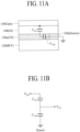
- FIG. 11B The relation between the capacitance Cap and the voltage according to FIG. 11A can be represented as shown in FIG. 11B .
- FIG. 11B due to the capacitance C CH between the channel portion 130n and the first connection portion 130a (Source), not all gate voltages V GS are effectively applied to the channel portion 130n. As a result, voltage loss can be generated.
- the third active layer 133 can include at least one of, for example, an IGZO(InGaZnO)-based oxide semiconductor material, a GZO(GaZnO)-based oxide semiconductor material, an IGO(InGaO)-based oxide semiconductor material, or a GZTO(GaZnSnO)-based oxide semiconductor material.
- an IGZO(InGaZnO)-based oxide semiconductor material a GZO(GaZnO)-based oxide semiconductor material, an IGO(InGaO)-based oxide semiconductor material, or a GZTO(GaZnSnO)-based oxide semiconductor material.
- the oxide semiconductor material constituting the third active layer 133 includes gallium (Ga) and indium (In)
- a concentration of gallium (Ga) is set to be higher than that of indium (In) based on the number of moles [Ga concentration > In concentration].
- the third active layer 133 is disposed in the first non-overlap area NOA1 and also serves as a protective layer for protecting the second active layer 132, an effect of increasing the carrier due to the third active layer 133 is not significant. Therefore, an s-factor of the thin film transistor 300 can be maintained at a high level.
- the carrier of the first non-overlap area NOA1 is not increased.
- an s-factor of the thin film transistor 400 can be maintained at a high level.
- FIG. 5A is a plan view illustrating a thin film transistor 500 according to further still another example of the present disclosure
- FIG. 5B is a cross-sectional view taken along line IV-IV' of FIG. 5A
- the thin film transistor 500 of FIG. 5A further includes a second non-overlap area NOA2 as compared with the thin film transistor 100 of FIG. 1A .
- the third active layer 133 can be disposed in the first overlap area OA1, the first non-overlap area NOA1 and the second non-overlap area NOA2.
- the third active layer 133 can also be disposed to cover the entire upper surface of the second active layer 132, but the present disclosure is not limited thereto, and the third active layer 133 can cover a portion of the upper surface of the second active layer 132.
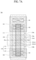
- FIG. 7A is a plan view illustrating a thin film transistor 700 according to further still another example of the present disclosure
- FIG. 7B is a cross-sectional view taken along line IVa-IVa' of FIG. 7A .
- the active layer 130 can include a third active layer 133 on the second active layer 132, and the third active layer 133 can be disposed on a portion of the upper surface of the second active layer 132.
- the third active layer 133 can be disposed in the first overlap area OA1.
- the third active layer 133 may not be disposed in the first non-overlap area NOA1.
- the third active layer 133 may not be disposed in the second non-overlap area NOA2.
- the third active layer 133 is not disposed in the second non-overlap area NOA2, so that a carrier of the second non-overlap area NOA2 may not be increased. As a result, an s-factor of the thin film transistor 700 can be maintained at a high level.
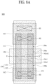
- the channel portion 130n can further include a second overlap area OA2 in which the first active layer 131 and the second active layer 132 overlap each other based on the plan view.
- the second overlap area OA2 can be spaced apart from the first overlap area OA1 and extend from the first connection portion 130a to the second connection portion 130b.
- the first overlap area OA1 and the second overlap area OA2 can be spaced apart from each other with the first non-overlap area NOA1 interposed therebetween.
- the first active layer 131 is not disposed in the first non-overlap area NOA1, and can be disposed in the first overlap area OA1 and the second overlap area OA2.
- the second overlap area OA2 includes a carrier (electron carrier) of a concentration higher than that of the first non-overlap area NOA1 in the same manner as the first overlap area OA1. Therefore, the second overlap area OA2 can serve to improve the ON-current of the thin film transistor 100 in the same manner as the first overlap area OA1.
- FIG. 9A is a plan view illustrating a thin film transistor 900 according to further still another example of the present disclosure
- FIG. 9B is a cross-sectional view taken along line Va-Va' of FIG. 9A
- the active layer 130 can further include a third active layer 133 on the second active layer 132.
- the third active layer 133 can be extended from the first connection portion 130a to the second connection portion 130b in the channel portion 130n.
- the third active layer 133 can be also disposed in the first connection portion 130a and the second connection portion 130b.
- FIG. 10A is a plan view illustrating a thin film transistor 1000 according to further still another example of the present disclosure
- FIG. 10B is a cross-sectional view taken along the line Vb-Vb' of FIG. 10A
- the active layer 130 can include a third active layer 133 on the second active layer 132, and the third active layer 133 can be disposed on a portion of the upper surface of the second active layer 132.
- the third active layer 133 can be disposed in the first overlap area OA1 and the second overlap area OA2.
- the third active layer 133 may not be disposed in the first non-overlap area NOA1.
- the carrier of the first non-overlap area NOA1 is not increased.
- an s-factor of the thin film transistor 1000 can be maintained at a high level.
- FIG. 13A is a graph illustrating a relation between an s-factor and an ON-current.
- FIG. 13B is a graph illustrating threshold voltages of thin film transistors. Referring to FIG. 13A , in the thin film transistor in which the light shielding layer 111 is disposed, when the thickness of the buffer layer BUF 120 is increased or the thickness of the gate insulating layer GI 140 is reduced, the ON-current of the thin film transistor can be increased, but the s-factor can be reduced.
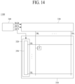
- the gate control signal GCS includes a gate start pulse GSP, a gate shift clock GSC, a gate output enable signal GOE, a start signal Vst and a gate clock GCLK. Also, control signals for controlling a shift register can be included in the gate control signal GCS.
- the data control signal DCS includes a source start pulse SSP, a source shift clock signal SSC, a source output enable signal SOE and a polarity control signal POL.
- the data driver 330 supplies a data voltage to the data lines DL of the display panel 310.
- the data driver 330 converts the image data RGB input from the controller 340 into an analog data voltage and supplies the data voltage to the data lines DL.
- the gate driver 320 may include a shift register 350.
- the shift register 350 supplies a gate-off signal capable of turning off the switching device, to the gate line GL for the other period of one frame, at which the gate pulse is not supplied.
- a gate pulse and the gate-off signal will be collectively referred to as a scan signal SS or Scan.
- the gate driver 320 can be packaged on the substrate 110.
- a structure in which the gate driver 320 is directly packaged on the substrate 110 will be referred to as a Gate In Panel (GIP) structure.
- GIP Gate In Panel
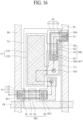
- FIG. 15 is a circuit view illustrating any one pixel P of FIG. 14
- FIG. 16 is a plan view illustrating a pixel P of FIG. 14
- FIG. 17 is a cross-sectional view taken along line VI-VI' of FIG. 16 .
- the circuit view of FIG. 15 is an equivalent circuit view for the pixel P of the display apparatus 1100 that includes an organic light emitting diode (OLED) as a display device 710.
- OLED organic light emitting diode
- the pixel P includes a display device 710 and a pixel driving circuit PDC for driving the display device 710.
- the pixel driving circuit PDC of FIG. 15 includes a first thin film transistor TR1 that is a switching transistor and a second thin film transistor TR2 that is a driving transistor.
- the thin film transistors 100, 200, 300, 400, 500, 600, 700, 800, 900 and 1000 described in the examples can be used as the second thin film transistor TR2.
- the thin film transistors 100, 200, 300, 400, 500, 600, 700, 800, 900 and 1000 described in the examples can be also used as the first thin film transistor TR1.
- the first thin film transistor TR1 is connected to the gate line GL and the data line DL, and is turned on or off by the scan signal SS supplied through the gate line GL.
- the data line DL provides a data voltage Vdata to the pixel driving circuit PDC, and the first thin film transistor TR1 controls applying of the data voltage Vdata.
- a driving power line PL provides a driving voltage Vdd to the display device 710, and the second thin film transistor TR2 controls the driving voltage Vdd.
- the driving voltage Vdd is a pixel driving voltage for driving the organic light emitting diode (OLED) that is the display device 710.
- the drain electrode D1 of the first thin film transistor TR1 and the source electrode S2 of the second thin film transistor TR2 are disposed on the interlayer insulating layer 170.
- the drain electrode D1 of the first thin film transistor TR1 can be connected to the active layer A1 of the first thin film transistor TR1 through a contact hole H12.
- the drain electrode D1 of the first thin film transistor TR1 can be connected to the first capacitor electrode CE1 through a contact hole H13.
- the data voltage can be applied to the first capacitor electrode CE1 and the gate electrode G2 of the second thin film transistor TR2.
- a bank layer 750 is disposed at an edge of the first electrode 711.
- the bank layer 750 defines a light emission area of the display device 710.
- An organic light emitting layer 712 is further disposed on the first electrode 711, and a second electrode 713 is disposed on the organic light emitting layer 712. Therefore, the display device 710 is completed.
- the display device 710 shown in FIG. 17 is an organic light emitting diode (OLED). Therefore, the display apparatus 1100 according to one example of the present disclosure is an organic light emitting display apparatus.
- the data voltage Vdata is supplied to the data line DL
- the scan signal SS is supplied to the gate line GL
- the driving voltage Vdd for driving the pixel is supplied to the driving power line PL
- a reference voltage Vref is supplied to a reference line RL
- a sensing control signal SCS is supplied to a sensing control line SCL.
- the data voltage Vdata supplied through the data line DL is supplied to the gate electrode G2 of the second thin film transistor TR2.
- the data voltage Vdata is charged in the first capacitor C1 formed between the gate electrode G2 and the source electrode S2 of the second thin film transistor TR2.
- the second thin film transistor TR2 is turned on, the current is supplied to the display device 710 through the second thin film transistor TR2 in accordance with the driving voltage Vdd for driving the pixel, whereby light is output from the display device 710.
Landscapes
- Physics & Mathematics (AREA)
- Geometry (AREA)
- Engineering & Computer Science (AREA)
- Microelectronics & Electronic Packaging (AREA)
- Thin Film Transistor (AREA)
- Devices For Indicating Variable Information By Combining Individual Elements (AREA)
- Electroluminescent Light Sources (AREA)
Abstract
Description
- This application claims the benefit of the
Korean Patent Application No. 10-2022-0184668 filed on December 26, 2022 - The present disclosure relates to a thin film transistor and a display apparatus comprising the same.
- Transistors are widely used as switching devices or driving devices in the field of electronic apparatuses. In particular, because a thin film transistor can be manufactured on a glass substrate or a plastic substrate, the thin film transistor is widely used as a switching device of a display apparatus such as a liquid crystal display apparatus or an organic light emitting apparatus.
- The display apparatus may include, for example, a switching thin film transistor and a driving thin film transistor. Generally, it is preferable that the driving thin film transistor has a large s-factor (or sub-threshold swing) to represent a gray scale. However, the thin film transistors generally have a small s-factor to ensure on-off characteristics. Thus, when thin film transistors are applied to the driving thin film transistor of the display apparatus, it is difficult to represent a gray scale of the display apparatus.
- Therefore, the thin film transistor applied to the driving thin film transistor of the display apparatus also needs to have a large s-factor to easily represent a gray scale. Also, even though the thin film transistor has a large s-factor, the thin film transistor should have excellent current characteristics in an ON-state.
- The present disclosure has been made in view of the above problems and it is an object of the present disclosure to provide a thin film transistor that has a large s-factor and has excellent current characteristics in an ON-state.
- It is another object of the present disclosure to provide a thin film transistor having a large current value in an ON-state while having a large s-factor by partially stacking two different types of oxide semiconductor layers to form a two-channel structure.
- It is still another object of the present disclosure to provide a thin film transistor designed such that an interval between a gate electrode and an active layer is not greater than necessary to have excellent ON-current characteristics as the interval between the gate electrode and the active layer does not need to be increased to increase an s-factor of the thin film transistor.
- It is further still another object of the present disclosure to provide a display apparatus including a driving thin film transistor having a large s-factor and large ON-current characteristics to have an excellent gray scale representation capability and excellent current characteristics.
- In addition to the objects of the present disclosure as mentioned above, additional objects and features of the present disclosure will be clearly understood by those skilled in the art from the following description of the present disclosure.
- In accordance with an aspect of the present disclosure, the above and other objects are accomplished by including a thin film transistor having an active layer, and a gate electrode at least partially overlapped with the active layer. Further, the active layer includes a channel portion (e.g. a channel), a first connection portion contacting one side of the channel portion, and a second connection portion contacting the other side of the channel portion, the active layer includes a first active layer and a second active layer on the first active layer, the channel portion includes a first overlap area in which the first active layer and the second active layer overlap each other based on a plan view (from above), and a first non-overlap area in which the first active layer and the second active layer do not overlap each other based on the plan view. Also, each of the first active layer and the second active layer extends from the first connection portion to the second connection portion in the channel portion. In this instance, the second active layer can have a mobility greater (electron mobility) than a mobility of the first active layer.
- In addition, the first overlap area can extend from the first connection portion to the second connection portion, and first non-overlap area can extend from the first connection portion to the second connection portion. The second active layer can cover an entire upper surface of the first active layer in the channel portion, and the second active layer can be disposed in an entire area of the channel portion based on the plan view. Also, the first active layer is not disposed in the first non-overlap area.
- The active layer may further include a third active layer on the second active layer, and the third active layer can extend from the first connection portion to the second connection portion in the channel portion. The third active layer can also have a mobility smaller than a mobility of the second active layer. Also, the third active layer can be disposed in the first overlap area and the first non-overlap area. However, the third active layer may not be disposed in the first non-overlap area.
- In addition, the channel portion can further include a second non-overlap area in which the first active layer and the second active layer do not overlap each other based on the plan view, and the second non-overlap area can be spaced apart from the first non-overlap area and may extend from the first connection portion to the second connection portion. The first active layer may not be disposed in the second non-overlap area.
- Further, the active layer can further include a third active layer on the second active layer, and the third active layer can extend from the first connection portion to the second connection portion in the channel portion. The third active layer can also have a mobility smaller than a mobility of the second active layer, and be disposed in the first overlap area, the first non-overlap area and the second non-overlap area. Also, the third active layer may not be disposed in the second non-overlap area.
- In addition, the channel portion can further include a second overlap area in which the first active layer and the second active layer overlap each other based on the plan view, and the second overlap area can be spaced apart from the first overlap area, and thus can extend from the first connection portion to the second connection portion.
- The active layer can further include a third active layer on the second active layer, and the third active layer can extend from the first connection portion to the second connection portion in the channel portion. The third active layer can also have a mobility smaller than a mobility of the second active layer, and be disposed in the first overlap area, the first non-overlap area and the second overlap area. However, the third active layer may not be disposed in the first non-overlap area.
- In addition, the first active layer can include at least one of an IGZO(InGaZnO)-based oxide semiconductor material, a GZO(GaZnO)-based oxide semiconductor material, an IGO(InGaO)-based oxide semiconductor material, or a GZTO(GaZnSnO)-based oxide semiconductor material, and when the oxide semiconductor material of the first active layer includes gallium (Ga) and indium (In), a concentration of gallium (Ga) may be higher than a concentration of indium (In) based on the number of moles [Ga concentration > In concentration].
- The second active layer may include at least one of an IGZO(InGaZnO)-based oxide semiconductor material, an IZO(InZnO)-based oxide semiconductor material, an ITZO(InSnZnO)-based oxide semiconductor material, an IGZTO(InGaZnSnO)-based oxide semiconductor material, a FIZO(FeInZnO)-based semiconductor material, a ZnO-based oxide semiconductor material, a SIZO(SiInZnO)-based oxide semiconductor material, or a ZnON(Zn-Oxynitride)-based oxide semiconductor material, and when the oxide semiconductor material of the second active layer includes gallium (Ga) and indium (In), a concentration of indium (In) may be higher than a concentration of gallium (Ga) based on the number of moles [Ga concentration < In concentration].
- In accordance with another aspect of the present disclosure, the above and other objects can be accomplished by the provision of a display apparatus comprising the above-described thin film transistor.
- The above and other objects, features and advantages of the present disclosure will be more clearly understood from the following detailed description taken in conjunction with the accompanying drawings, in which:
-
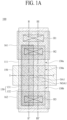
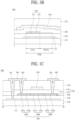
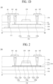
FIG. 1A is a plan view illustrating a thin film transistor according to one example of the present disclosure,FIG. 1B is a cross-sectional view taken along line I-I' ofFIG. 1A ,FIG. 1C is a cross-sectional view taken along line II-II' ofFIG. 1A , andFIG. 1D is a cross-sectional view taken along line III-III' ofFIG. 1A ; -
FIG. 2 is a cross-sectional view illustrating a thin film transistor according to another example of the present disclosure; -
FIG. 3A is a plan view illustrating a thin film transistor according to still another example of the present disclosure, and 3B is a cross-sectional view taken along line Ia-Ia' ofFIG. 3A ; -
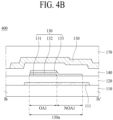
FIG. 4A is a plan view illustrating athin film transistor 400 according to still another example of the present disclosure, andFIG. 4B is a cross-sectional view taken along line Ib-Ib' ofFIG. 4A ; -
FIG. 5A is a plan view illustrating a thin film transistor according to still another example of the present disclosure, and 5B is a cross-sectional view taken along line IV-IV' ofFIG. 5A ; -
FIG. 6 is a cross-sectional view illustrating a thin film transistor according to further still another example of the present disclosure; -
FIG. 7A is a plan view illustrating athin film transistor 700 according to further still another example of the present disclosure, andFIG. 7B is a cross-sectional view taken along line IVa-IVa' ofFIG. 7A ; -
FIG. 8A is a plan view illustrating a thin film transistor according to further still another example of the present disclosure, and 8B is a cross-sectional view taken along line V-V' ofFIG. 8A ; -
FIG. 9A is a plan view illustrating athin film transistor 900 according to further still another example of the present disclosure, andFIG. 9B is a cross-sectional view taken along line Va-Va' ofFIG. 9A ; -
FIG. 10A is a plan view illustrating athin film transistor 1000 according to further still another example of the present disclosure, andFIG. 10B is a cross-sectional view taken along the line Vb-Vb' ofFIG. 10A ; -
FIGS. 11A and 11B are schematic views illustrating a gate voltage applied to a thin film transistor; -
FIGS. 12A and 12B are schematic views illustrating a gate voltage applied to a thin film transistor; -
FIG. 13A is a graph illustrating a relation between an s-factor and an ON-current, andFIG. 13B is a graph illustrating threshold voltages of thin film transistors; -
FIG. 14 is a schematic view illustrating a display apparatus according to another example of the present disclosure; -
FIG. 15 is a circuit view illustrating any one pixel ofFIG. 14 ; -
FIG. 16 is a plan view illustrating the pixel ofFIG. 14 ; -
FIG. 17 is a cross-sectional view taken along line VI-VI' ofFIG. 16 ; -
FIG. 18 is a circuit view illustrating any one pixel of a display apparatus according to still another example of the present disclosure; and -
FIG. 19 is a circuit view illustrating any one pixel of a display apparatus according to further still another example of the present disclosure. - Advantages and features of the present disclosure, and implementation methods thereof will be clarified through following examples described with reference to the accompanying drawings. The present disclosure may, however, be embodied in different forms and should not be construed as limited to the examples set forth herein. Rather, these examples are provided so that this disclosure will be thorough and complete, and will fully explain the present disclosure to those skilled in the art.
- A shape, a size, a ratio, an angle, and a number disclosed in the drawings for describing examples of the present disclosure are merely an example, and thus, the present disclosure is not limited to the illustrated details. Like reference numerals refer to like elements throughout the specification.
- When `comprise', 'have', and 'include' described in the present specification are used, another part may be added unless 'only~' is used. The terms of a singular form may include plural forms unless referred to the contrary. In construing an element, the element is construed as including an error range although there is no explicit description. In describing a position relationship, for example, when the position relationship is described as 'upon~', 'above~', 'below~', and 'next to~', one or more portions may be arranged between two other portions unless 'just' or 'direct' is used.
- Spatially relative terms such as "below", "beneath", "lower", "above", and "upper" may be used herein to easily describe a relationship of one element or elements to another element or elements as illustrated in the figures. These terms are intended to encompass different orientations of the device in addition to the orientation depicted in the figures. For example, if the device illustrated in the figure is reversed, the device described to be arranged "below," or "beneath" another device may be arranged "above" another device. Therefore, an exemplary term "below or beneath" may include "below or beneath" and "above" orientations. Likewise, an exemplary term "above" or "on" may include "above" and "below or beneath" orientations.
- In describing a temporal relationship, for example, when the temporal order is described as "after," "subsequent," "next," and "before," a case which is not continuous may be included, unless "just" or "direct" is used. Although the terms "first", "second ," etc. may be used herein to describe various elements, these elements should not be limited by these terms. These terms are only used to partition one element from another. For example, a first element could be termed a second element, and, similarly, a second element could be termed a first element, without departing from the scope of the present invention.
- The term "at least one" should be understood as including any and all combinations of one or more of the associated listed items. For example, the meaning of "at least one of a first item, a second item, and a third item" denotes the combination of all items proposed from two or more of the first item, the second item, and the third item as well as the first item, the second item, or the third item.
- Features of various examples of the present disclosure can be partially or overall coupled to or combined with each other, and be variously inter-operated with each other and driven technically as those skilled in the art can sufficiently understand. The examples of the present disclosure can be performed independently from each other, or be performed together in a co-dependent relationship.
- In the drawings, the same or similar elements are denoted by the same reference numerals even though they are depicted in different drawings. In the examples of the present disclosure, a source electrode and a drain electrode are distinguished from each other, for convenience of description. However, the source electrode and the drain electrode may be used interchangeably. Further, the source electrode can be the drain electrode, and the drain electrode can be the source electrode. Also, the source electrode in any one example of the present disclosure can be the drain electrode in another example of the present disclosure, and the drain electrode in any one example of the present disclosure can be the source electrode in another example of the present disclosure.
- In some examples of the present disclosure, for convenience of description, a source region is distinguished from a source electrode, and a drain region is distinguished from a drain electrode. However, the examples of the present disclosure are not limited to this structure. For example, a source region can be a source electrode, and a drain region can be a drain electrode. Also, a source region can be a drain electrode, and a drain region can be a source electrode. In addition, in some examples of the present disclosure, the term "channel" may mean "channel portion", and the term "channel portion" may mean "channel".
- Next,
FIG. 1A is a plan view illustrating a thin film transistor according to one example of the present disclosure,FIG. 1B is a cross-sectional view taken along line I-I' ofFIG. 1A ,FIG. 1C is a cross-sectional view taken along line II-II' ofFIG. 1A , andFIG. 1D is a cross-sectional view taken along line III-III' ofFIG. 1A . - As shown, a
thin film transistor 100 according to one example of the present disclosure includes anactive layer 130 and agate electrode 150 that at least partially overlaps theactive layer 130. Theactive layer 130 includes achannel portion 130n, afirst connection portion 130a contacting one side of thechannel portion 130n, and asecond connection portion 130b contacting the other side of thechannel portion 130n. Also, theactive layer 130 includes a firstactive layer 131 and a secondactive layer 132 on the firstactive layer 131. In the examples of the present disclosure, the channel portion can be referred to as "channel", and thechannel portion 130n may be referred to as "channel 130n". - In addition, as shown in
FIG. 1B , thechannel portion 130n includes a first overlap area OA1 in which the firstactive layer 131 and the secondactive layer 132 overlap each other based on the plan view, and a first non-overlap area NOA1 in which the firstactive layer 131 and the secondactive layer 132 do not overlap each other based on the plan view. In thechannel portion 130n, each of the firstactive layer 131 and the secondactive layer 132 is extended from thefirst connection portion 130a to thesecond connection portion 130b. - Hereinafter, the
thin film transistor 100 according to one example of the present disclosure will be described in more detail with reference toFIGS. 1A to 1D . Referring toFIGS. 1A to 1D , thethin film transistor 100 is disposed on asubstrate 110. Glass or plastic can be used as thesubstrate 110. A transparent plastic having a flexible property, for example, polyimide can be used as the plastic. When polyimide is used as thesubstrate 110, a heat-resistant polyimide capable of enduring a high temperature can be used considering that a high temperature deposition process is performed on thesubstrate 110. - Also, a
light shielding layer 111 can be disposed on thesubstrate 110. Thelight shielding layer 111 has light shielding characteristics to shield light incident from the outside, thereby protecting thechannel portion 130n. Thelight shielding layer 111 can be disposed to overlap at least thechannel portion 130n of theactive layer 130. - Further, the
light shielding layer 111 can include a metal, and have electrical conductivity. For example, thelight shielding layer 111 may include at least one of an aluminum-based metal such as aluminum (Al) or an aluminum alloy, a silver-based metal such as silver (Ag) or a silver alloy, a copper-based metal such as copper (Cu) or a copper alloy, a molybdenum-based metal such as molybdenum (Mo) or a molybdenum alloy, chromium (Cr), tantalum (Ta), neodymium (Nd), titanium (Ti), or iron (Fe). Thelight shielding layer 111 can also have a multi-layered structure that includes at least two conductive layers having different respective physical properties. - A
buffer layer 120 is also disposed on thesubstrate 110 and thelight shielding layer 111. Thebuffer layer 120 can include at least one selected from silicon oxide, silicon nitride or metal-based oxide as an insulating material. Thebuffer layer 120 can also have a single-layered structure or a multi-layered structure. - Further, the
buffer layer 120 planarizes an upper portion of thesubstrate 110. In addition, thebuffer layer 120 can have air and moisture barrier properties and insulating properties to protect thethin film transistor 100. Thebuffer layer 120 also allows thelight shielding layer 111 and thechannel portion 130n to be spaced apart from and insulated from each other. - As shown, the
active layer 130 is disposed on thebuffer layer 120. Theactive layer 130 can be formed by a semiconductor material. According to one example of the present disclosure, theactive layer 130 may include an oxide semiconductor material. - Referring to
FIGS. 1A to 1D , theactive layer 130 includes a firstactive layer 131 and a secondactive layer 132 on the firstactive layer 131. The firstactive layer 131 can be disposed to overlap the secondactive layer 132. In addition, the secondactive layer 132 can have a mobility greater than that of the firstactive layer 131. As a result, in thethin film transistor 100, the secondactive layer 132 may serve as a main layer of a current flow. According to one example of the present disclosure, the secondactive layer 132 can have a mobility that is twice or greater than that of the firstactive layer 131. The secondactive layer 132 can have a mobility of 2 to 5 times as compared with the firstactive layer 131. - For example, the first
active layer 131 can have a mobility of 5cm2/V·s to 25cm2/V·s. In more detail, the firstactive layer 131 can have a mobility of 5cm2/V·s to 15 cm2/V·s, or can have a mobility of about 10 cm2/V·s. The secondactive layer 132 can have a mobility of 20cm2/V·s or more. In more detail, the secondactive layer 132 can have a mobility of 20cm2/V·s to 50cm2/V·s. In more detail, the secondactive layer 132 can have a mobility in the range of 20cm2/V·s to 40cm2/V·s or 20cm2/V·s to 30cm2/V·s. - Further, the second
active layer 132 can have a mobility greater than that of the firstactive layer 131 as much as 10cm2/V·s to 40cm2/V·s. The secondactive layer 132 can have a mobility greater than that of the firstactive layer 131 as much as 10cm2/V·s to 30 cm2/V·s, 10cm2/V·s to 20cm2/V·s, or 20cm2/V·s to 30cm2/V·s. - The first
active layer 131 can include an oxide semiconductor material having excellent stability. In addition, the firstoxide semiconductor layer 131 supports the secondoxide semiconductor layer 132. Therefore, the firstoxide semiconductor layer 131 is also referred to as a "support layer." The firstactive layer 131 can include at least one of, for example, an IGZO(InGaZnO)-based oxide semiconductor material, a GZO(GaZnO)-based oxide semiconductor material, an IGO(InGaO)-based oxide semiconductor material, or a GZTO(GaZnSnO)-based oxide semiconductor material. When the oxide semiconductor material constituting the firstactive layer 131 includes gallium (Ga) and indium (In), a concentration of gallium (Ga) is set to be higher than that of indium (In) based on the number of moles [Ga concentration > In concentration]. - The second
active layer 132 can include an oxide semiconductor material having high mobility. The secondactive layer 132 may include at least one of, for example, an IGZO(InGaZnO)-based oxide semiconductor material, an IZO(InZnO)-based oxide semiconductor material, an ITZO(InSnZnO)-based oxide semiconductor material, an IGZTO(InGaZnSnO)-based oxide semiconductor material, a FIZO(FeInZnO)-based semiconductor material, a ZnO-based oxide semiconductor material, a SIZO(SiInZnO)-based oxide semiconductor material, or a ZnON(Zn-Oxynitride)-based oxide semiconductor material. When the oxide semiconductor material constituting the secondactive layer 132 includes gallium (Ga) and indium (In), a concentration of indium (In) is set to be higher than that of gallium (Ga) based on the number of moles [Ga concentration < In concentration]. - However, the type of the oxide semiconductor material is not limited to the above example, and the first
active layer 131 and the secondactive layer 132 can include other oxide semiconductor materials known in the art. Referring toFIGS. 1A ,1C and1D , theactive layer 130 includes achannel portion 130n, afirst connection portion 130a contacting one side of thechannel portion 130n, and asecond connection portion 130b contacting the other side of thechannel portion 130n. - The
channel portion 130n overlaps thegate electrode 150, and serves as a channel of thethin film transistor 100. One side of thechannel portion 130n contacts thefirst connection portion 130a, and the other side of thechannel portion 130n contacts thesecond connection portion 130b. - As shown, the
first connection portion 130a and thesecond connection portion 130b of theactive layer 130 do not overlap thegate electrode 150. In addition, thefirst connection portion 130a and thesecond connection portion 130b can be formed by selective conductorization of a semiconductor material. According to one example of the present disclosure, providing a conductivity to a selected portion of theactive layer 130 will be referred to as selective conductorization. The selective conductorization can be performed by doping, plasma treatment or the like. - For example, selective conductorization for the
active layer 130 can be performed by dopant doping using thegate electrode 150 or photoresist as a mask. Implantation of dopant ions into a selected area of theactive layer 130 will be referred to as dopant doping. The dopant may include at least one of, for example, boron (B), phosphorus (P), fluorine (F) or hydrogen (H). - When the selective conductorization for the
active layer 130 is performed by dopant doping or implantation, an area doped with a dopant in theactive layer 130 is selectively conductorized to become thefirst connection portion 130a or thesecond connection portion 130b. An area of theactive layer 130, which is not doped with a dopant, is not conductorized, and becomes thechannel portion 130n. - In addition, the selective conductorization for the
active layer 130 can be performed by plasma treatment applied to a process of patterning agate insulating layer 140. For example, plasma can be used in the process of patterning thegate insulating layer 140, and a portion of theactive layer 130, which is in contact with the plasma, can be selectively conductorized to become thefirst connection portion 130a or thesecond connection portion 130b. A portion of theactive layer 130, which is protected by thegate insulating layer 140 and does not contact the plasma, is not conductorized, and can become thechannel portion 130n. - The
first connection portion 130a and thesecond connection portion 130b are portions made of an oxide semiconductor material and then given conductivity. Therefore, thefirst connection portion 130a and thesecond connection portion 130b have a greater electrical conductivity than that of thechannel portion 130n. That is, by conductorization, thefirst connection portion 130a and thesecond connection portion 130b can have an electrical conductivity similar to that of a metal used as an electrical wiring. - Referring to
FIG. 1C , thechannel portion 130n may include a channel portion 131n of the firstactive layer 131 and achannel portion 132n of the secondactive layer 132. Thefirst connection portion 130a includes afirst connection portion 131a of the firstactive layer 131 and afirst connection portion 132a of the secondactive layer 132. Also, thesecond connection portion 130b includes a second connection portion 131b of the firstactive layer 131 and asecond connection portion 132b of the secondactive layer 132. - Further, the
first connection portion 130a of theactive layer 130 can be a source area, and thesecond connection portion 130b thereof can be a drain area. Therefore, thefirst connection portion 130a can serve as a source electrode, and thesecond connection portion 130b can serve as a drain electrode. However, the present disclosure is not limited to the above example, and thefirst connection portion 130a can be a drain area, and thesecond connection portion 130b can be a source area. - In addition, the
channel portion 130n includes a first overlap area OA1 in which the firstactive layer 131 and the secondactive layer 132 overlap each other based on a plan view, and a first non-overlap area NOA1 in which the firstactive layer 131 and the secondactive layer 132 do not overlap each other based on the plan view. - As shown, each of the first
active layer 131 and the secondactive layer 132 in thechannel portion 130n extends from thefirst connection portion 130a to thesecond connection portion 130b. As a result, the first overlap area OA1 can extend from thefirst connection portion 130a to thesecond connection portion 130b. In addition, the first non-overlap area NOA1 can be extend from thefirst connection portion 130a to thesecond connection portion 130b. - Because the first overlap area OA1 and the first non-overlap area NOA1 can be extended from the
first connection portion 130a to thesecond connection portion 130b, both the first overlap area OA1 and the first non-overlap area NOA1 can serve as channels of thethin film transistor 100. - Referring to
FIGS. 1A and1B , the secondactive layer 132 can be disposed in the entire area of thechannel portion 130n based on the plan view. In addition, the firstactive layer 131 can be disposed only in the first overlap area OA1 without being disposed in the first non-overlap area NOA1. According to one example of the present disclosure, in thechannel portion 130n, the secondactive layer 132 can cover an entire upper surface of the firstactive layer 131. -
FIG. 1C is a cross-sectional view illustrating a first overlap area OA1, andFIG. 1D is a cross-sectional view illustrating a first non-overlap area NOA1. As shown inFIGS. 1C and1D , the firstactive layer 131 and the secondactive layer 132 are disposed to overlap each other in the first overlap area OA1, whereas only the secondactive layer 132 is disposed in the first non-overlap area NOA1. Therefore, the first overlap area OA1 can have a carrier that is more abundant than that of the first non-overlap area NOA1. In more detail, the first overlap area OA1 can have an electron carrier that is more abundant than that of the first non-overlap area NOA1. - As a result, the ON-current of the
thin film transistor 100 can be improved by the first overlap area OA1. Therefore, thethin film transistor 100 having the first overlap area OA1 can have excellent current characteristics. - Also, the first non-overlap area NOA1 has a carrier having a concentration lower than that of the first overlap area OA1. In more detail, the first non-overlap area NOA1 can have an electron carrier of a concentration lower than that of the first overlap area OA1. Therefore, before the
thin film transistor 100 is completely turned on by applying a gate voltage, a current increase rate of the thin film transistor can be delayed. As a result, an s-factor (sub-threshold swing) of thethin film transistor 100 can be increased. - As described above, the
channel portion 130n includes the first overlap area OA1 and the first non-overlap area NOA1 together, so that the ON-current of thethin film transistor 100 can be improved and at the same time, the s-factor can be increased. - Referring to
FIGS. 1B-1D , thegate insulating layer 140 is disposed on theactive layer 130 and protects thechannel portion 130n. Thegate insulating layer 140 can include at least one of silicon oxide, silicon nitride or metal-based oxide and can have a single-layered structure or a multi-layered structure. - Referring to
FIGS. 1B to 1D , thegate insulating layer 140 can be integrally formed on the entire surface of thesubstrate 110, but the present disclosure is not limited thereto, and thegate insulating layer 140 can be patterned. For example, thegate insulating layer 140 can be patterned to have a shape corresponding to that of thegate electrode 150. - Further, the
gate electrode 150 is disposed on thegate insulating layer 140 and overlaps thechannel portion 130n of theactive layer 130. Thegate electrode 150 can include at least one of an aluminum-based metal such as aluminum (Al) or an aluminum alloy, a silver-based metal such as silver (Ag) or a silver alloy, a copper-based metal such as copper (Cu) or a copper alloy, a molybdenum-based metal such as molybdenum (Mo) or a molybdenum alloy, chromium (Cr), tantalum (Ta), neodymium (Nd), or titanium (Ti). Thegate electrode 150 can also have a multi-layered structure that includes at least two conductive layers having their respective physical properties different from each other. - An interlayer insulating
layer 170 is disposed on thegate electrode 150 and is an insulating layer made of an insulating material. The interlayer insulatinglayer 170 can be made of an organic material or an inorganic material, or can be made of a stacked body of an organic material layer and an inorganic material layer. - A
source electrode 161 and adrain electrode 162 are disposed on theinterlayer insulating layer 170. As shown, thesource electrode 161 is connected to theactive layer 130 through a contact hole H2. In more detail, thesource electrode 161 can be electrically connected to thefirst connection portion 130a of theactive layer 130 through the contact hole H2. The source electrode 161 can also be connected to thelight shielding layer 111 through a contact hole H1. As a result, thelight shielding layer 111 can be connected to thefirst connection portion 130a of theactive layer 130. - In addition, the
drain electrode 162 is spaced apart from thesource electrode 161 and is thus connected to theactive layer 130 through a contact hole H3. In more detail, thedrain electrode 162 can be electrically connected to thesecond connection portion 130b of theactive layer 130 through a contact hole H3. - Each of the
source electrode 161 and thedrain electrode 162 can include at least one of molybdenum (Mo), aluminum (Al), chromium (Cr), gold (Au), titanium (Ti), nickel (Ni), neodymium (Nd), copper (Cu) or their alloy. Each of thesource electrode 161 and thedrain electrode 162 can also be formed of a single layer made of a metal or a metal alloy, or can be formed of a multi-layer of two or more layers. - However, the present disclosure is not limited to the above example, and the
first connection portion 130a can be a source electrode and an electrode indicated by a reference numeral "161" can be a connection electrode or a bridge. Likewise, thesecond connection portion 130b can be a drain electrode and an electrode indicated by a reference numeral "162" can be a connection electrode or a bridge. - Hereinafter, the s-factor will be described in more detail. At a threshold voltage Vth of a drain-source current graph for a gate voltage of the
thin film transistor 100, the s-factor (sub-threshold swing) can be used as an index indicating a change level of the drain-source current for the gate voltage. The s-factor can be described by a current-change graph shown inFIG. 13B , for example. - In particular,
FIG. 13B illustrates a drain-source current IDS for a gate voltage VGS. At the threshold voltage Vth of thethin film transistor 100, a reciprocal of a slope in the graph of the drain-source current IDS for the gate voltage VGS can be defined as the s-factor. When the slope of the graph is steep, the s-factor is small, and when the slope of the graph is small, the s-factor is large. When the s-factor is large, a change rate of the drain-source current IDS for the gate voltage at a period of the threshold voltage Vth is slow. When the s-factor is large, since the change rate of the drain-source current IDS for the gate voltage is slow, it is easy to adjust a magnitude of the drain-source current IDS by adjusting the gate voltage VGS. - In the display apparatus driven by the current, for example, in an organic light emitting display apparatus, a gray scale of a pixel can be controlled by adjusting the magnitude of the drain-source current IDS of the driving thin film transistor. The magnitude of the drain-source current IDS of the driving thin film transistor is determined by the gate voltage. Therefore, in the organic light emitting display apparatus driven by the current, it is easy to adjust a gray scale of a pixel as the s-factor of the driving thin film transistor TR becomes large.
- As a method for adjusting the s-factor of the
thin film transistor 100 includes adjusting a thickness of thegate insulating layer 140. In more detail,FIGS. 11A and 11B are schematic views illustrating a gate voltage applied to a thin film transistor. - As shown,
FIG. 11A schematically illustrates a capacitance Cap that can be generated when a gate voltage VGS is applied to the thin film transistor. In particular,FIG. 11A schematically illustrates a relation of the capacitance Cap and a voltage before the thin film transistor is completely turned on. InFIG. 11A , the gate voltage VGS is a voltage between thesource electrode 161 and thegate electrode 150. The gate voltage VGS can be referred to as a voltage between thefirst connection portion 130a and thegate electrode 150. - As shown in
FIG. 11A , when the gate voltage VGS is applied to the thin film transistor, a capacitance CGI can be formed between thechannel portion 130n of theactive layer 130 and the gate electrode 150 (Gate), and a capacitance CCH can be also formed between thechannel portion 130n and thefirst connection portion 130a (Source). The capacitance CCH formed between thechannel portion 130n and thefirst connection portion 130a (Source) can be referred to as a capacitance formed by a voltage difference between thedrain electrode 162, which is a high voltage terminal, and thesource electrode 161, which is a low voltage terminal, in thechannel portion 130n made of an oxide semiconductor layer having N-type semiconductor characteristics. - The relation between the capacitance Cap and the voltage according to
FIG. 11A can be represented as shown inFIG. 11B . Referring toFIG. 11B , due to the capacitance CCH between thechannel portion 130n and thefirst connection portion 130a (Source), not all gate voltages VGS are effectively applied to thechannel portion 130n. As a result, voltage loss can be generated. - Referring to
FIG. 11B , when one of the gate voltages VGS, which is effectively applied to thechannel portion 130n during driving of the thin film transistor, is referred to as an effective gate voltage Veff, the effective gate voltage Veff can be obtained by the followingEquation 1.
- In order to increase the s-factor of the
thin film transistor 100, when the thickness of thegate insulating layer 140 is increased, a capacitance CGI is reduced between thechannel portion 130n of theactive layer 130 and the gate electrode 150 (Gate), so that an effective gate voltage Veff, which is effectively applied to thechannel portion 130n, among the gate voltages VGS can be reduced. As a result, the s-factor can be increased, but the effective gate voltage Veff calculated by theEquation 1 is also reduced, and the ON-Current of thethin film transistor 100 is reduced. - On the other hand, according to one example of the present disclosure, because the
channel portion 130n includes the first overlap area OA1 and the first non-overlap area NOA1 together, the s-factor of thethin film transistor 100 can be increased without reducing the ON-Current. - Next,
FIGS. 12A and 12B are schematic views illustrating a gate voltage applied to thethin film transistor 100 and describing an example that thelight shielding layer 111 is connected to thesource electrode 161. As shown inFIG. 12A , when the gate voltage VGS is applied to thethin film transistor 100, the capacitance CGI can be formed between thechannel portion 130n of theactive layer 130 and thegate electrode 150, the capacitance CCH can be formed between thechannel portion 130n and thefirst connection portion 130a (Source), and a capacitance CBUF can be additionally formed between thechannel portion 130n and thelight shielding layer 111. - The relation between the capacitance Cap and the voltage according to
FIG. 12A can be represented as shown inFIG. 12B . Referring toFIG. 12B , due to the capacitance CCH between thechannel portion 130n and thefirst connection portion 130a (Source) and the capacitance CBUF between thechannel portion 130n and thelight shielding layer 111, not all gate voltages VGS are effectively applied to thechannel portion 130n, and voltage loss can be generated. - When the
light shielding layer 111 and thesource electrode 161 are electrically connected to each other, the capacitance CBUF is additionally generated between thechannel portion 130n and thelight shielding layer 111, so that a lower capacitance CCH + CBUF causing a voltage loss is increased. In more detail, when a voltage of the gate voltages VGS, which is effectively applied to thechannel portion 130n, is referred to as the effective gate voltage Veff inFIG. 12B , the effective gate voltage Veff can be obtained by the followingEquation 2.
- Referring to the
Equation 2, a denominator value of theEquation 2 is increased due to the capacitance CBUF formed between thechannel portion 130n and thelight shielding layer 111. Therefore, when the capacitance CBUF between thechannel portion 130n and thelight shielding layer 111 is increased, the effective gate voltage Veff is reduced, whereby the increase rate of the drain-source current IDS in thethin film transistor 100 is reduced. As a result, the s-factor is increased. - Referring to the
Equation 2, the capacitance CBUF between thechannel portion 130n and thelight shielding layer 111 can be increased to increase the s-factor of thethin film transistor 100. A method for increasing the capacitance CBUF between thechannel portion 130n and thelight shielding layer 111 includes reducing a thickness of thebuffer layer 120. However, when the thickness of thebuffer layer 120 is reduced, thechannel portion 130n of thethin film transistor 100 can be damaged by hydrogen, oxygen or moisture, and the ON-current of thethin film transistor 100 is reduced. - According to one example of the present disclosure, because the
channel portion 130n includes the first overlap area OA1 and the first non-overlap area NOA1 together, the s-factor of thethin film transistor 100 can be increased even though the thickness of thebuffer layer 120 is not reduced, and at the same time the ON-current of thethin film transistor 100 can be also increased. - Next,
FIG. 2 is a cross-sectional view illustrating athin film transistor 200 according to another example of the present disclosure. In particular,FIG. 2 corresponds to a cross-section taken along line II-II' ofFIG. 1A . Referring toFIG. 2 , thegate insulating layer 140 can be patterned without being formed on the entire surface of thesubstrate 110. For example, as shown inFIG. 2 , thegate insulating layer 140 can be patterned in the same planar shape as that of thegate electrode 150. - In addition,
FIG. 3A is a plan view illustrating athin film transistor 300 according to still another example of the present disclosure, andFIG. 3B is a cross-sectional view taken along line Ia-Ia' ofFIG. 3A . Referring toFIGS. 3A and3B , theactive layer 130 can further include a thirdactive layer 133 on the secondactive layer 132. The thirdactive layer 133 can be extended from thefirst connection portion 130a to thesecond connection portion 130b in thechannel portion 130n. The thirdactive layer 133 can also be also disposed in thefirst connection portion 130a and thesecond connection portion 130b. - Further, the third
active layer 133 can protect the secondactive layer 132. To protect the secondactive layer 132, the thirdactive layer 133 can be made of an oxide semiconductor material having an excellent stability. The thirdactive layer 133 can also serve as a protective layer for protecting the secondactive layer 132. - In addition, the third
active layer 133 can have a mobility smaller than that of the thirdactive layer 133. The secondactive layer 132 can have a mobility greater than that of the thirdactive layer 133 as much as two times or more. In more detail, the secondactive layer 132 can have a mobility of 2 to 5 times as compared with the thirdactive layer 133. The thirdactive layer 133 can have a mobility of 5cm2/V·s to 25cm2/V·s. In more detail, the thirdactive layer 133 can have a mobility of 5cm2/V·s to 15cm2/V·s, or can have mobility of about 10 cm2/V·s. - Further, the second
active layer 132 can have a mobility greater than that of the thirdactive layer 133 as much as 10cm2/V·s to 40cm2/V·s. The secondactive layer 132 can also have a mobility greater than that of the thirdactive layer 133 as much as 10cm2/V·s to 30 cm2/V·s, 10cm2/V·s to 20cm2/V·s, or 20cm2/V·s to 30cm2/V·s. - The third
active layer 133 can include at least one of, for example, an IGZO(InGaZnO)-based oxide semiconductor material, a GZO(GaZnO)-based oxide semiconductor material, an IGO(InGaO)-based oxide semiconductor material, or a GZTO(GaZnSnO)-based oxide semiconductor material. When the oxide semiconductor material constituting the thirdactive layer 133 includes gallium (Ga) and indium (In), a concentration of gallium (Ga) is set to be higher than that of indium (In) based on the number of moles [Ga concentration > In concentration]. - Thus, with the third
active layer 133, the secondactive layer 132, which is an intermediate layer in the manufacturing process, can be effectively protected. For example, in the manufacturing process, the firstactive layer 131 can protect the secondactive layer 132, which is an intermediate layer, from gas, for example, hydrogen (H), moisture (H2O), oxygen (O2), etc. generated from thebuffer layer 120 therebelow or another insulating layer, and the thirdactive layer 133 can protect the secondactive layer 132, which is an intermediate layer, from an etching solution used during a patterning process or gas, for example, hydrogen (H), moisture (H2O), oxygen (O2), etc. generated from an upper insulating layer, for example, thegate insulating layer 140, theinterlayer insulating layer 170, etc. - Referring to
FIGS. 3A and3B , the thirdactive layer 133 can be disposed in the first overlap area OA1 and the first non-overlap area NOA1. The thirdactive layer 133 can be disposed to cover the entire upper surface of the secondactive layer 132, but the present disclosure is not limited thereto, and the thirdactive layer 133 can cover a portion of the upper surface of the secondactive layer 132. - Referring to
FIGS. 3A and3B , because the thirdactive layer 133 is disposed in the first non-overlap area NOA1 and also serves as a protective layer for protecting the secondactive layer 132, an effect of increasing the carrier due to the thirdactive layer 133 is not significant. Therefore, an s-factor of thethin film transistor 300 can be maintained at a high level. - Next,
FIG. 4A is a plan view illustrating athin film transistor 400 according to still another example of the present disclosure, andFIG. 4B is a cross-sectional view taken along line Ib-Ib' ofFIG. 4A . Referring toFIGS. 4A and4B , theactive layer 130 can include a thirdactive layer 133 on the secondactive layer 132, and the thirdactive layer 133 can be disposed on a portion of the upper surface of the secondactive layer 132. In more detail, the thirdactive layer 133 is not disposed in the first non-overlap area NOA1 and is disposed only in the first overlap area OA1. - The third
active layer 133 is disposed in the first overlap area OA1, so that the upper portion of the secondactive layer 132 can be effectively protected in at least the first overlap area OA1. In addition, the electron carrier of the first overlap area OA1 can be increased due to the carrier included in the thirdactive layer 133. In a structural aspect, a thickness of the first overlap area OA1 is increased due to the thirdactive layer 133, whereby the physical stability of the first overlap area OA1 can be improved. As a result, the stability of thethin film transistor 100 can be improved, and the ON-current of thethin film transistor 100 can be improved by the first overlap area OA1. On the other hand, as the thirdactive layer 133 is not disposed in the first non-overlap area NOA1, the carrier of the first non-overlap area NOA1 is not increased. As a result, an s-factor of thethin film transistor 400 can be maintained at a high level. - Next,
FIG. 5A is a plan view illustrating athin film transistor 500 according to further still another example of the present disclosure, andFIG. 5B is a cross-sectional view taken along line IV-IV' ofFIG. 5A . Thethin film transistor 500 ofFIG. 5A further includes a second non-overlap area NOA2 as compared with thethin film transistor 100 ofFIG. 1A . - Referring to
FIGS. 5A and5B , thechannel portion 130n can further include a second non-overlap area NOA in which the firstactive layer 131 and the secondactive layer 132 do not overlap each other based on the plan view. The second non-overlap area NOA2 can be spaced apart from the first non-overlap area NOA1 and extend from thefirst connection portion 130a to thesecond connection portion 130b. The first non-overlap area NOA1 and the second non-overlap area NOA2 can be disposed to be spaced apart from each other with the first overlap area OA1 interposed therebetween. - As shown, the first
active layer 131 may not be disposed in the second non-overlap area NOA2. Further, the second non-overlap area NOA2 includes a carrier (electron carrier) having a concentration lower than that of the first overlap area OA1 in the same manner as the first non-overlap area NOA1. Therefore, the second non-overlap area NOA2 can serve to increase the s-factor of thethin film transistor 100 in the same manner as the first non-overlap area NOA1. - Next,
FIG. 6 is a cross-sectional view illustrating athin film transistor 600 according to further still another example of the present disclosure. In particular,FIG. 6 is a cross-sectional view taken along line IV-IV' ofFIG. 5A . - Referring to
FIG. 6 , theactive layer 130 can further include a thirdactive layer 133 on the secondactive layer 132. The thirdactive layer 133 can be extended from thefirst connection portion 130a to thesecond connection portion 130b in thechannel portion 130n. The thirdactive layer 133 can also be disposed in thefirst connection portion 130a and thesecond connection portion 130b. - In addition, the third
active layer 133 can be disposed in the first overlap area OA1, the first non-overlap area NOA1 and the second non-overlap area NOA2. The thirdactive layer 133 can also be disposed to cover the entire upper surface of the secondactive layer 132, but the present disclosure is not limited thereto, and the thirdactive layer 133 can cover a portion of the upper surface of the secondactive layer 132. - Referring to
FIG. 6 , the thirdactive layer 133 is disposed in the first non-overlap area NOA1 and the second non-overlap area NOA2, but an effect of increasing the carrier due to the thirdactive layer 133 is not significant. Therefore, an s-factor of thethin film transistor 600 can be maintained at a high level. - Next,
FIG. 7A is a plan view illustrating athin film transistor 700 according to further still another example of the present disclosure, andFIG. 7B is a cross-sectional view taken along line IVa-IVa' ofFIG. 7A . Referring toFIGS. 7A and7B , theactive layer 130 can include a thirdactive layer 133 on the secondactive layer 132, and the thirdactive layer 133 can be disposed on a portion of the upper surface of the secondactive layer 132. - In more detail, the third
active layer 133 can be disposed in the first overlap area OA1. The thirdactive layer 133 may not be disposed in the first non-overlap area NOA1. In addition, the thirdactive layer 133 may not be disposed in the second non-overlap area NOA2. The thirdactive layer 133 is not disposed in the second non-overlap area NOA2, so that a carrier of the second non-overlap area NOA2 may not be increased. As a result, an s-factor of thethin film transistor 700 can be maintained at a high level. - Next,
FIG. 8A is a plan view illustrating athin film transistor 800 according to further still another example of the present disclosure, andFIG. 8B is a cross-sectional view taken along the line V-V' ofFIG. 8A . Thethin film transistor 800 ofFIG. 8A further includes a second overlap area OA2 as compared with thethin film transistor 100 ofFIG. 1A . - Referring to
FIGS. 8A and8B , thechannel portion 130n can further include a second overlap area OA2 in which the firstactive layer 131 and the secondactive layer 132 overlap each other based on the plan view. The second overlap area OA2 can be spaced apart from the first overlap area OA1 and extend from thefirst connection portion 130a to thesecond connection portion 130b. In addition, the first overlap area OA1 and the second overlap area OA2 can be spaced apart from each other with the first non-overlap area NOA1 interposed therebetween. - According to one example of the present disclosure, the first
active layer 131 is not disposed in the first non-overlap area NOA1, and can be disposed in the first overlap area OA1 and the second overlap area OA2. Also, the second overlap area OA2 includes a carrier (electron carrier) of a concentration higher than that of the first non-overlap area NOA1 in the same manner as the first overlap area OA1. Therefore, the second overlap area OA2 can serve to improve the ON-current of thethin film transistor 100 in the same manner as the first overlap area OA1. -
FIG. 9A is a plan view illustrating athin film transistor 900 according to further still another example of the present disclosure, andFIG. 9B is a cross-sectional view taken along line Va-Va' ofFIG. 9A . Referring toFIGS. 9A and9B , theactive layer 130 can further include a thirdactive layer 133 on the secondactive layer 132. As shown, the thirdactive layer 133 can be extended from thefirst connection portion 130a to thesecond connection portion 130b in thechannel portion 130n. The thirdactive layer 133 can be also disposed in thefirst connection portion 130a and thesecond connection portion 130b. - Further, the third
active layer 133 can be disposed in the first overlap area OA1, the first non-overlap area NOA1 and the second overlap area OA2. Also, the thirdactive layer 133 can be disposed to cover the entire upper surface of the secondactive layer 132, but the present disclosure is not limited thereto, and the thirdactive layer 133 can cover a portion of the upper surface of the secondactive layer 132. - Referring to
FIGS. 9A and9B , the thirdactive layer 133 is disposed in the first non-overlap area NOA1, but the effect of increasing the carrier due to the thirdactive layer 133 is not significant. Therefore, an s-factor of thethin film transistor 900 can be maintained at a high level. - Next,
FIG. 10A is a plan view illustrating athin film transistor 1000 according to further still another example of the present disclosure, andFIG. 10B is a cross-sectional view taken along the line Vb-Vb' ofFIG. 10A . Referring toFIGS. 10A and10B , theactive layer 130 can include a thirdactive layer 133 on the secondactive layer 132, and the thirdactive layer 133 can be disposed on a portion of the upper surface of the secondactive layer 132. In more detail, the thirdactive layer 133 can be disposed in the first overlap area OA1 and the second overlap area OA2. The thirdactive layer 133 may not be disposed in the first non-overlap area NOA1. - As the third
active layer 133 is not disposed in the first non-overlap area NOA1, the carrier of the first non-overlap area NOA1 is not increased. As a result, an s-factor of thethin film transistor 1000 can be maintained at a high level. - As described previously,
FIGS. 11A and 11B are schematic views illustrating a gate voltage applied to a thin film transistor in which thelight shielding layer 111 is not disposed, andFIGS. 12A and 12B are schematic views illustrating a gate voltage applied to a thin film transistor in which thelight shielding layer 111 is disposed. - As described previously,
FIG. 13A is a graph illustrating a relation between an s-factor and an ON-current. In addition,FIG. 13B is a graph illustrating threshold voltages of thin film transistors. Referring toFIG. 13A , in the thin film transistor in which thelight shielding layer 111 is disposed, when the thickness of thebuffer layer BUF 120 is increased or the thickness of the gate insulatinglayer GI 140 is reduced, the ON-current of the thin film transistor can be increased, but the s-factor can be reduced. - On the other hand, in the thin film transistor in which the
light shielding layer 111 is disposed, when the thickness of thebuffer layer BUF 120 is reduced or the thickness of the gate insulatinglayer GI 140 is increased, the s-factor of the thin film transistor can be increased, but the ON-current can be reduced. -
FIG. 13B illustrates threshold voltages of various thin film transistors. InFIG. 13B , "Example 1" is a threshold voltage graph for thethin film transistor 100 ofFIG. 1 , "Comparative Example 1" is a threshold voltage graph of a thin film transistor in which the thickness of thegate insulating layer 140 is reduced to improve the ON-Current, and "Comparative Example 2" is a threshold voltage graph of a thin film transistor in which the thickness of thegate insulating layer 140 is increased to improve the s-factor. - Referring to the "Comparative Example 1 ," when the thickness of the
gate insulating layer 140 is reduced, the ON-current of the thin film transistor is improved but the s-factor is reduced. In addition, referring to the "Comparative Example 2 ," when the thickness of thegate insulating layer 140 is increased, the s-factor of the thin film transistor is increased but the ON-current is reduced. On the other hand, the thin film transistor of the Example 1 according to example 1 of the present disclosure has excellent ON-current characteristics while having a large s-factor. - Hereinafter, the display apparatus comprising the above-described
thin film transistors FIG. 14 is a schematic view illustrating adisplay apparatus 1100 according to further still another example of the present disclosure. - As shown in
FIG. 14 , thedisplay apparatus 1100 according to further still another example of the present disclosure includes adisplay panel 310, agate driver 320, adata driver 330 and acontroller 340. Gate lines GL and data lines DL are disposed in thedisplay panel 310, and pixels P are disposed in intersection areas of the gate lines GL and the data lines DL. An image is displayed by driving of the pixels P. - The
controller 340 controls thegate driver 320 and thedata driver 330. In addition, thecontroller 340 outputs a gate control signal GCS for controlling thegate driver 320 and a data control signal DCS for controlling thedata driver 330 by using a signal supplied from an external system. Also, thecontroller 340 samples input image data input from the external system, realigns the sampled data and supplies the realigned digital image data RGB to thedata driver 330. - The gate control signal GCS includes a gate start pulse GSP, a gate shift clock GSC, a gate output enable signal GOE, a start signal Vst and a gate clock GCLK. Also, control signals for controlling a shift register can be included in the gate control signal GCS. The data control signal DCS includes a source start pulse SSP, a source shift clock signal SSC, a source output enable signal SOE and a polarity control signal POL.
- The
data driver 330 supplies a data voltage to the data lines DL of thedisplay panel 310. In more detail, thedata driver 330 converts the image data RGB input from thecontroller 340 into an analog data voltage and supplies the data voltage to the data lines DL. Thegate driver 320 may include ashift register 350. - In addition, the
shift register 350 sequentially supplies gate pulses to the gate lines GL for one frame by using the start signal and the gate clock, which are transmitted from thecontroller 340. In this instance, one frame means a time period at which one image is output through thedisplay panel 310. The gate pulse has a turn-on voltage capable of turning on a switching device (thin film transistor) disposed in the pixel P. - Also, the
shift register 350 supplies a gate-off signal capable of turning off the switching device, to the gate line GL for the other period of one frame, at which the gate pulse is not supplied. Hereinafter, the gate pulse and the gate-off signal will be collectively referred to as a scan signal SS or Scan. - According to one example of the present disclosure, the
gate driver 320 can be packaged on thesubstrate 110. In this way, a structure in which thegate driver 320 is directly packaged on thesubstrate 110 will be referred to as a Gate In Panel (GIP) structure. - Next,
FIG. 15 is a circuit view illustrating any one pixel P ofFIG. 14 ,FIG. 16 is a plan view illustrating a pixel P ofFIG. 14 , andFIG. 17 is a cross-sectional view taken along line VI-VI' ofFIG. 16 . The circuit view ofFIG. 15 is an equivalent circuit view for the pixel P of thedisplay apparatus 1100 that includes an organic light emitting diode (OLED) as adisplay device 710. - As shown, the pixel P includes a
display device 710 and a pixel driving circuit PDC for driving thedisplay device 710. The pixel driving circuit PDC ofFIG. 15 includes a first thin film transistor TR1 that is a switching transistor and a second thin film transistor TR2 that is a driving transistor. For example, thethin film transistors thin film transistors - As shown, the first thin film transistor TR1 is connected to the gate line GL and the data line DL, and is turned on or off by the scan signal SS supplied through the gate line GL. The data line DL provides a data voltage Vdata to the pixel driving circuit PDC, and the first thin film transistor TR1 controls applying of the data voltage Vdata.
- A driving power line PL provides a driving voltage Vdd to the
display device 710, and the second thin film transistor TR2 controls the driving voltage Vdd. In addition, the driving voltage Vdd is a pixel driving voltage for driving the organic light emitting diode (OLED) that is thedisplay device 710. - When the first thin film transistor TR1 is turned on by the scan signal SS applied from the
gate driver 320 through the gate line GL, the data voltage Vdata supplied through the data line DL is supplied to a gate electrode G2 of the second thin film transistor TR2 connected with thedisplay device 710. Further, the data voltage Vdata is charged in a first capacitor C1 formed between the gate electrode G2 and a source electrode S2 of the second thin film transistor TR2. The first capacitor C1 is a storage capacitor Cst. - The amount of a current supplied to the organic light emitting diode (OLED), which is the
display device 710, through the second thin film transistor TR2 is controlled in accordance with the data voltage Vdata, whereby a gray scale of light emitted from thedisplay device 710 can be controlled. - Referring to
FIGS. 16 and17 , the first thin film transistor TR1 and the second thin film transistor TR2 are disposed on thesubstrate 110. Thesubstrate 110 can be made of glass or plastic. Plastic having a flexible property, for example, polyimide (PI) can be used as thesubstrate 110. - The
light shielding layer 111 is disposed on thesubstrate 110. Referring toFIGS. 16 and17 , thelight shielding layer 111 is disposed only below the second thin film transistor TR2 that is a driving transistor, but the present disclosure is not limited thereto, and thelight shielding layer 111 can be also disposed below the first thin film transistor TR1. - A
buffer layer 120 is disposed on thelight shielding layer 111. Thebuffer layer 120 is made of an insulating material, and protects active layers A1 and A2 from external moisture or oxygen. The active layer A1 of the first thin film transistor TR1 and the active layer A2 of the second thin film transistor TR2 are disposed on thebuffer layer 120. The active layers A1 and A2 may include, for example, a firstactive layer 131, a secondactive layer 132 and a thirdactive layer 133. The active layers A1 and A2 can have any one of the structures ofFIGS. 3 ,4 ,6 ,7 ,9 and10 . - In addition, a
gate insulating layer 140 is disposed on the active layers A1 and A2. Thegate insulating layer 140 may cover entire upper surfaces of the active layers A1 and A2, or may cover only a portion of the active layers A1 and A2. The gate electrode G1 of the first thin film transistor TR1 and the gate electrode G2 of the second thin film transistor TR2 are disposed on thegate insulating layer 140. Also, a first capacitor electrode CE1 can be disposed on thegate insulating layer 140. The first capacitor electrode CE1 can be connected to the gate electrode G2 of the second thin film transistor TR2. - An interlayer insulating
layer 170 is disposed on the gate electrodes G1 and G2 and the first capacitor electrode CE1. The data line DL, the driving power line PL, source electrodes S1 and S2 and drain electrodes D1 and D2 are disposed on theinterlayer insulating layer 170. A portion of the data line DL can be extended to become the source electrode S1 of the first thin film transistor TR1. The source electrode S1 of the first thin film transistor TR1 can be connected to the active layer A1 of the first thin film transistor TR1 through a contact hole H11. - Referring to
FIGS. 16 and17 , the drain electrode D1 of the first thin film transistor TR1 and the source electrode S2 of the second thin film transistor TR2 are disposed on theinterlayer insulating layer 170. The drain electrode D1 of the first thin film transistor TR1 can be connected to the active layer A1 of the first thin film transistor TR1 through a contact hole H12. In addition, the drain electrode D1 of the first thin film transistor TR1 can be connected to the first capacitor electrode CE1 through a contact hole H13. As a result, the data voltage can be applied to the first capacitor electrode CE1 and the gate electrode G2 of the second thin film transistor TR2. - The source electrode S2 of the second thin film transistor TR2 can be connected to the
light shielding layer 111 through one contact hole H14, and can be connected to the active layer A2 of the second thin film transistor TR2 through another contact hole H15. As a result, thelight shielding layer 111 can be connected to the source electrode S2 of the second thin film transistor TR2. - In addition, the source electrode S2 of the second thin film transistor TR2 can be extended to become a second capacitor electrode CE2. The second capacitor electrode CE2 overlaps the first capacitor electrode CE1 to form the first capacitor C1. A portion of the driving power line PL can be extended to become the drain electrode D2 of the second thin film transistor TR2. The drain electrode D2 of the second thin film transistor TR2 can be connected to the active layer A2 of the second thin film transistor TR2 through a contact hole H16.
- A
planarization layer 180 is disposed on the data line DL, the driving power line PL, the source electrodes S1 and S2, the drain electrodes D1 and D2 and the second capacitor electrode CE2. Theplanarization layer 180 planarizes upper portions of the first thin film transistor TR1 and the second thin film transistor TR2 and protects the first thin film transistor TR1 and the second thin film transistor TR2. - Further, a
first electrode 711 of thedisplay device 710 is disposed on theplanarization layer 180. Thefirst electrode 711 of thedisplay device 710 contacts the source electrode S2 of the second thin film transistor TR2 and the second capacitor electrode CE2 through a contact hole H17 formed in theplanarization layer 180. - Also, a
bank layer 750 is disposed at an edge of thefirst electrode 711. Thebank layer 750 defines a light emission area of thedisplay device 710. An organiclight emitting layer 712 is further disposed on thefirst electrode 711, and asecond electrode 713 is disposed on the organiclight emitting layer 712. Therefore, thedisplay device 710 is completed. Thedisplay device 710 shown inFIG. 17 is an organic light emitting diode (OLED). Therefore, thedisplay apparatus 1100 according to one example of the present disclosure is an organic light emitting display apparatus. - According to another example of the present disclosure, the second thin film transistor TR2 can have a large s-factor. The second thin film transistor TR2 can be used as a driving transistor to improve a gray scale representation capability of the
display apparatus 1100. - Next,
FIG. 18 is a circuit view illustrating any one pixel P of adisplay apparatus 1200 according to further still another example of the present disclosure. In particular,FIG. 18 is an equivalent circuit view illustrating a pixel P of an organic light emitting display apparatus. - The pixel P of the
display apparatus 1200 shown inFIG. 18 includes an organic light emitting diode (OLED) that is adisplay device 710 and a pixel driving circuit PDC for driving thedisplay device 710. Thedisplay device 710 is connected with the pixel driving circuit PDC. In the pixel P, signal lines DL, GL, PL, RL and SCL for supplying a signal to the pixel driving circuit PDC are disposed. - The data voltage Vdata is supplied to the data line DL, the scan signal SS is supplied to the gate line GL, the driving voltage Vdd for driving the pixel is supplied to the driving power line PL, a reference voltage Vref is supplied to a reference line RL, and a sensing control signal SCS is supplied to a sensing control line SCL.
- Referring to
FIG. 18 , assuming that a gate line of an (n)th pixel P is "GLn ," a gate line of an (n-1)th pixel P adjacent to the (n)th pixel P is "GLn-1" and the gate line "GLn-1" of the (n-1)th pixel P serves as a sensing control line SCL of the (n)th pixel P. The pixel driving circuit PDC includes, for example, a first thin film transistor TR1 (switching transistor) connected with the gate line GL and the data line DL, a second thin film transistor TR2 (driving transistor) for controlling a magnitude of a current output to thedisplay device 710 in accordance with the data voltage Vdata transmitted through the first thin film transistor TR1, and a third thin film transistor TR3 (reference transistor) for sensing characteristics of the second thin film transistor TR2. - A first capacitor C1 is positioned between the gate electrode G2 of the second thin film transistor TR2 and the
display device 710. The first capacitor C1 is referred to as a storage capacitor Cst. The first thin film transistor TR1 is turned on by the scan signal SS supplied to the gate line GL to transmit the data voltage Vdata, which is supplied to the data line DL, to the gate electrode G2 of the second thin film transistor TR2. - The third thin film transistor TR3 is connected to a first node n1 between the second thin film transistor TR2 and the
display device 710 and the reference line RL, and thus is turned on or off by the sensing control signal SCS and senses characteristics of the second thin film transistor TR2, which is a driving transistor, for a sensing period. A second node n2 connected with the gate electrode G2 of the second thin film transistor TR2 is connected with the first thin film transistor TR1. The first capacitor C1 is formed between the second node n2 and the first node n1. - When the first thin film transistor TR1 is turned on, the data voltage Vdata supplied through the data line DL is supplied to the gate electrode G2 of the second thin film transistor TR2. The data voltage Vdata is charged in the first capacitor C1 formed between the gate electrode G2 and the source electrode S2 of the second thin film transistor TR2. When the second thin film transistor TR2 is turned on, the current is supplied to the
display device 710 through the second thin film transistor TR2 in accordance with the driving voltage Vdd for driving the pixel, whereby light is output from thedisplay device 710. - Next,
FIG. 19 is a circuit view illustrating any one pixel of adisplay apparatus 1300 according to further still another example of the present disclosure. The pixel P of thedisplay apparatus 1300 shown inFIG. 19 includes an organic light emitting diode (OLED) that is adisplay device 710 and a pixel driving circuit PDC for driving thedisplay device 710. Thedisplay device 710 is connected with the pixel driving circuit PDC. - The pixel driving circuit PDC includes thin film transistors TR1, TR2, TR3 and TR4. In the pixel P, signal lines DL, EL, GL, PL, SCL and RL for supplying a driving signal to the pixel driving circuit PDC are disposed. In comparison with the pixel P of
FIG. 18 , the pixel P ofFIG. 19 further includes an emission control line EL. An emission control signal EM is supplied to the emission control line EL. Also, the pixel driving circuit PDC ofFIG. 19 further includes a fourth thin film transistor TR4 that is an emission control transistor for controlling a light emission timing of the second thin film transistor TR2, in comparison with the pixel driving circuit PDC ofFIG. 18 . - Referring to
FIG. 19 , assuming that a gate line of an (n)th pixel P is "GLn ," a gate line of an (n-1)th pixel P adjacent to the (n)th pixel P is "GLn-1" and the gate line "GLn-1" of the (n-1)th pixel P serves as a sensing control line SCL of the (n)th pixel P. A first capacitor C1 is positioned between the gate electrode G2 of the second thin film transistor TR2 and thedisplay device 710. Also, a second capacitor C2 is positioned between one of terminals of the fourth thin film transistor TR4, to which a driving voltage Vdd is supplied, and one electrode of thedisplay device 710. - The first thin film transistor TR1 is turned on by the scan signal SS supplied to the gate line GL to transmit the data voltage Vdata, which is supplied to the data line DL, to the gate electrode G2 of the second thin film transistor TR2. The third thin film transistor TR3 is connected to the reference line RL, and thus is turned on or off by the sensing control signal SCS and senses characteristics of the second thin film transistor TR2, which is a driving transistor, for a sensing period.
- In addition, the fourth thin film transistor TR4 transfers the driving voltage Vdd to the second thin film transistor TR2 in accordance with the emission control signal EM, or shields the driving voltage Vdd. When the fourth thin film transistor TR4 is turned on, a current is supplied to the second thin film transistor TR2, whereby light is output from the
display device 710. The pixel driving circuit PDC according to further still another example of the present disclosure can be formed in various structures in addition to the above-described structure. The pixel driving circuit PDC may include, for example, five or more thin film transistors. - According to the present disclosure, the following advantages are obtained.
- The thin film transistor according to one example of the present disclosure has a large s-factor and at the same time has excellent ON-current characteristics. Therefore, when the thin film transistor is used in the display apparatus, a gray scale representation capability of the display apparatus can be improved, and current characteristics of the display apparatus can be also improved.
- Further examples are set out in the clauses below:
- 1. A thin film transistor comprising: an active layer; and a gate electrode at least partially overlapped with the active layer, wherein the active layer includes: a first active layer and a second active layer on the first active layer; a channel; a first connection portion contacting a first side of the channel; and a second connection portion contacting a second side of the channel, wherein the channel includes:
- a first overlap area in which the first active layer and the second active layer overlap each other based on a plan view; and
- a first non-overlap area in which the first active layer and the second active layer do not overlap each other based on the plan view, wherein in the channel of the active layer, each of the first active layer and the second active layer extends from the first connection portion to the second connection portion, and wherein the second active layer has a mobility greater than a mobility of the first active layer.
- 2. The thin film transistor of
clause 1, wherein the first overlap area of the channel extends from the first connection portion to the second connection portion. - 3. The thin film transistor of
clause 1 orclause 2, wherein the first non-overlap area of the channel extends from the first connection portion to the second connection portion. - 4. The thin film transistor of any one of the preceding clauses, wherein the second active layer covers an upper surface of the first active layer in the channel.
- 5. The thin film transistor of any one of the preceding clauses, wherein the second active layer is disposed in an area of the channel based on the plan view.
- 6. The thin film transistor of any one of the preceding clauses, wherein the first active layer is not disposed in the first non-overlap area of the channel.
- 7. The thin film transistor of any one of the preceding clauses, wherein the active layer further includes a third active layer on the second active layer, wherein the third active layer extends from the first connection portion to the second connection portion in the channel, and
wherein the third active layer has a mobility smaller than a mobility of the second active layer. - 8. The thin film transistor of clause 7, wherein the third active layer is disposed in the first overlap area and the first non-overlap area of the channel.
- 9. The thin film transistor of clause 7, wherein the third active layer is not disposed in the first non-overlap area of the channel.
- 10. The thin film transistor of any one of the preceding clauses, wherein the channel further includes a second non-overlap area in which the first active layer and the second active layer do not overlap each other based on the plan view, and wherein the second non-overlap area is spaced apart from the first non-overlap area and extends from the first connection portion to the second connection portion.
- 11. The thin film transistor of clause 10, wherein the first active layer is not disposed in the second non-overlap area of the channel.
- 12. The thin film transistor of clause 10, wherein the active layer further includes a third active layer on the second active layer, wherein the third active layer extends from the first connection portion to the second connection portion in the channel, and wherein the third active layer has a mobility smaller than a mobility of the second active layer.
- 13. The thin film transistor of clause 12, wherein the third active layer is disposed in the first overlap area, the first non-overlap area and the second non-overlap area of the channel.
- 14. The thin film transistor of clause 12, wherein the third active layer is not disposed in the second non-overlap area of the channel.
- 15. The thin film transistor of
clause 1, wherein the channel further includes a second overlap area in which the first active layer and the second active layer overlap each other based on the plan view, and wherein the second overlap area is spaced apart from the first overlap area, and extends from the first connection portion to the second connection portion. - 16. The thin film transistor of clause 15, wherein the active layer further includes a third active layer on the second active layer, wherein the third active layer extends from the first connection portion to the second connection portion in the channel, and wherein the third active layer has a mobility smaller than a mobility of the second active layer.
- 17. The thin film transistor of clause 16, wherein the third active layer is disposed in the first overlap area, the first non-overlap area and the second overlap area of the channel.
- 18. The thin film transistor of clause 16, wherein the third active layer is not disposed in the first non-overlap area of the channel.
- 19. The thin film transistor of any one of the preceding clauses, wherein the first active layer includes at least one of an IGZO (InGaZnO)-based oxide semiconductor material, a GZO (GaZnO)-based oxide semiconductor material, an IGO (InGaO)-based oxide semiconductor material, or a GZTO (GaZnSnO)-based oxide semiconductor material, and when the oxide semiconductor material of the first active layer includes gallium (Ga) and indium (In), a concentration of gallium (Ga) is higher than a concentration of indium (In) based on the number of moles [Ga concentration > In concentration].
- 20. The thin film transistor of any one of the preceding clauses, wherein the second active layer includes at least one of an IGZO (InGaZnO)-based oxide semiconductor material, an IZO (InZnO)-based oxide semiconductor material, an ITZO (InSnZnO)-based oxide semiconductor material, an IGZTO (InGaZnSnO)-based oxide semiconductor material, a FIZO (FeInZnO)-based semiconductor material, a ZnO-based oxide semiconductor material, a SIZO (SiInZnO)-based oxide semiconductor material, or a ZnON (Zn-Oxynitride)-based oxide semiconductor material, and when the oxide semiconductor material of the second active layer includes gallium (Ga) and indium (In), a concentration of indium (In) is higher than a concentration of gallium (Ga) based on the number of moles [Ga concentration < In concentration].
- 21. A display apparatus comprising the thin film transistor of any one of the preceding clauses.
- It will be apparent to those skilled in the art that the present disclosure described above is not limited by the above-described examples and the accompanying drawings and that various substitutions, modifications and variations can be made in the present disclosure without departing from the scope of the disclosures.
Claims (15)
- A thin film transistor comprising:an active layer; anda gate electrode at least partially overlapped with the active layer,wherein the active layer includes:a first active layer and a second active layer on the first active layer;a channel;a first connection portion contacting a first side of the channel; anda second connection portion contacting a second side of the channel,wherein the channel includes:a first overlap area in which the first active layer and the second active layer overlap each other based on a plan view; anda first non-overlap area in which the first active layer and the second active layer do not overlap each other based on the plan view,wherein in the channel of the active layer, each of the first active layer and the second active layer extends from the first connection portion to the second connection portion, andwherein the second active layer has a mobility greater than a mobility of the first active layer.
- The thin film transistor of claim 1, wherein the first overlap area of the channel extends from the first connection portion to the second connection portion.
- The thin film transistor of claim 1 or claim 2, wherein the first non-overlap area of the channel extends from the first connection portion to the second connection portion.
- The thin film transistor of any one of the preceding claims, wherein the second active layer covers an upper surface of the first active layer in the channel; or optionally
wherein the second active layer is disposed in an area of the channel based on the plan view. - The thin film transistor of any one of the preceding claims, wherein the first active layer is not disposed in the first non-overlap area of the channel.
- The thin film transistor of claim 1, wherein the active layer further includes a third active layer on the second active layer,wherein the third active layer extends from the first connection portion to the second connection portion in the channel, andwherein the third active layer has a mobility smaller than a mobility of the second active layer.
- The thin film transistor of claim 6, wherein the third active layer is disposed in the first overlap area and the first non-overlap area of the channel; or optionally wherein the third active layer is not disposed in the first non-overlap area of the channel.
- The thin film transistor of any one of the preceding claims, wherein the channel further includes a second non-overlap area in which the first active layer and the second active layer do not overlap each other based on the plan view, and
wherein the second non-overlap area is spaced apart from the first non-overlap area and extends from the first connection portion to the second connection portion. - The thin film transistor of claim 8, wherein the first active layer is not disposed in the second non-overlap area of the channel.
- The thin film transistor of claim 8, wherein the active layer further includes a third active layer on the second active layer,wherein the third active layer extends from the first connection portion to the second connection portion in the channel, andwherein the third active layer has a mobility smaller than a mobility of the second active layer.
- The thin film transistor of claim 10, wherein the third active layer is disposed in the first overlap area, the first non-overlap area and the second non-overlap area of the channel; or optionally wherein the third active layer is not disposed in the second non-overlap area of the channel.
- The thin film transistor of claim 1, wherein the channel further includes a second overlap area in which the first active layer and the second active layer overlap each other based on the plan view, and
wherein the second overlap area is spaced apart from the first overlap area, and extends from the first connection portion to the second connection portion. - The thin film transistor of claim 12, wherein the active layer further includes a third active layer on the second active layer,wherein the third active layer extends from the first connection portion to the second connection portion in the channel, andwherein the third active layer has a mobility smaller than a mobility of the second active layer; and optionallywherein the third active layer is disposed in the first overlap area, the first non-overlap area and the second overlap area of the channel; or optionallywherein the third active layer is not disposed in the first non-overlap area of the channel.
- The thin film transistor of any one of the preceding claims, wherein the first active layer includes at least one of an IGZO (InGaZnO)-based oxide semiconductor material, a GZO (GaZnO)-based oxide semiconductor material, an IGO (InGaO)-based oxide semiconductor material, or a GZTO (GaZnSnO)-based oxide semiconductor material, and when the oxide semiconductor material of the first active layer includes gallium (Ga) and indium (In), a concentration of gallium (Ga) is higher than a concentration of indium (In) based on the number of moles [Ga concentration > In concentration]; or optionally
wherein the second active layer includes at least one of an IGZO (InGaZnO)-based oxide semiconductor material, an IZO (InZnO)-based oxide semiconductor material, an ITZO (InSnZnO)-based oxide semiconductor material, an IGZTO (InGaZnSnO)-based oxide semiconductor material, a FIZO (FeInZnO)-based semiconductor material, a ZnO-based oxide semiconductor material, a SIZO (SiInZnO)-based oxide semiconductor material, or a ZnON (Zn-Oxynitride)-based oxide semiconductor material, and when the oxide semiconductor material of the second active layer includes gallium (Ga) and indium (In), a concentration of indium (In) is higher than a concentration of gallium (Ga) based on the number of moles [Ga concentration < In concentration]. - A display apparatus comprising the thin film transistor of any one of the preceding claims.
Applications Claiming Priority (1)
| Application Number | Priority Date | Filing Date | Title |
|---|---|---|---|
| KR1020220184668A KR20240102539A (en) | 2022-12-26 | 2022-12-26 | Thin film transistor and display apparatus comprising the same |
Publications (2)
| Publication Number | Publication Date |
|---|---|
| EP4394892A1 true EP4394892A1 (en) | 2024-07-03 |
| EP4394892B1 EP4394892B1 (en) | 2025-07-30 |
Family
ID=88016171
Family Applications (1)
| Application Number | Title | Priority Date | Filing Date |
|---|---|---|---|
| EP23196115.2A Active EP4394892B1 (en) | 2022-12-26 | 2023-09-07 | Thin film transistor and display apparatus comprising the same |
Country Status (6)
| Country | Link |
|---|---|
| US (1) | US20240213375A1 (en) |
| EP (1) | EP4394892B1 (en) |
| JP (1) | JP7685580B2 (en) |
| KR (1) | KR20240102539A (en) |
| CN (1) | CN118263284A (en) |
| TW (2) | TWI888317B (en) |
Cited By (2)
| Publication number | Priority date | Publication date | Assignee | Title |
|---|---|---|---|---|
| EP4686342A1 (en) * | 2024-07-24 | 2026-01-28 | LG Display Co., Ltd. | Thin film transistor, method for manufacturing the same and display apparatus comprising the same |
| EP4742230A1 (en) * | 2024-11-12 | 2026-05-13 | LG Display Co., Ltd. | Transistor and display device including the same |
Families Citing this family (1)
| Publication number | Priority date | Publication date | Assignee | Title |
|---|---|---|---|---|
| KR20260016695A (en) * | 2024-07-25 | 2026-02-04 | 삼성디스플레이 주식회사 | Transistor, display device comprising the same and manufacturing methode of the transistor |
Citations (2)
| Publication number | Priority date | Publication date | Assignee | Title |
|---|---|---|---|---|
| CN114628528A (en) * | 2020-12-14 | 2022-06-14 | 乐金显示有限公司 | Thin film transistor and display device including the same |
| KR20230067042A (en) * | 2021-11-09 | 2023-05-16 | 엘지디스플레이 주식회사 | Thin film transistor and display apparatus comprising the same |
Family Cites Families (7)
| Publication number | Priority date | Publication date | Assignee | Title |
|---|---|---|---|---|
| US9214474B2 (en) | 2011-07-08 | 2015-12-15 | Semiconductor Energy Laboratory Co., Ltd. | Semiconductor device and method for manufacturing semiconductor device |
| US9385238B2 (en) | 2011-07-08 | 2016-07-05 | Semiconductor Energy Laboratory Co., Ltd. | Transistor using oxide semiconductor |
| TWI658597B (en) | 2014-02-07 | 2019-05-01 | 日商半導體能源研究所股份有限公司 | Semiconductor device |
| TW201624708A (en) | 2014-11-21 | 2016-07-01 | 半導體能源研究所股份有限公司 | Semiconductor device and memory device |
| KR102573690B1 (en) * | 2016-09-30 | 2023-09-04 | 엘지디스플레이 주식회사 | Array Substrate for Thin Film Transistor And Display Device Of The Same |
| US11177449B2 (en) * | 2018-12-12 | 2021-11-16 | Industry-University Cooperation Foundation Hanyang University | P-type semiconductor layer, P-type multilevel element, and manufacturing method for the element |
| TWI883063B (en) * | 2019-11-08 | 2025-05-11 | 日商半導體能源研究所股份有限公司 | Display device, display module, and electronic device |
-
2022
- 2022-12-26 KR KR1020220184668A patent/KR20240102539A/en active Pending
-
2023
- 2023-08-23 TW TW113145856A patent/TWI888317B/en active
- 2023-08-23 TW TW112131723A patent/TWI868867B/en active
- 2023-08-29 US US18/457,520 patent/US20240213375A1/en active Pending
- 2023-09-07 EP EP23196115.2A patent/EP4394892B1/en active Active
- 2023-11-09 CN CN202311490266.4A patent/CN118263284A/en active Pending
- 2023-11-13 JP JP2023192686A patent/JP7685580B2/en active Active
Patent Citations (2)
| Publication number | Priority date | Publication date | Assignee | Title |
|---|---|---|---|---|
| CN114628528A (en) * | 2020-12-14 | 2022-06-14 | 乐金显示有限公司 | Thin film transistor and display device including the same |
| KR20230067042A (en) * | 2021-11-09 | 2023-05-16 | 엘지디스플레이 주식회사 | Thin film transistor and display apparatus comprising the same |
Cited By (2)
| Publication number | Priority date | Publication date | Assignee | Title |
|---|---|---|---|---|
| EP4686342A1 (en) * | 2024-07-24 | 2026-01-28 | LG Display Co., Ltd. | Thin film transistor, method for manufacturing the same and display apparatus comprising the same |
| EP4742230A1 (en) * | 2024-11-12 | 2026-05-13 | LG Display Co., Ltd. | Transistor and display device including the same |
Also Published As
| Publication number | Publication date |
|---|---|
| TWI888317B (en) | 2025-06-21 |
| CN118263284A (en) | 2024-06-28 |
| JP7685580B2 (en) | 2025-05-29 |
| KR20240102539A (en) | 2024-07-03 |
| TW202428147A (en) | 2024-07-01 |
| EP4394892B1 (en) | 2025-07-30 |
| TWI868867B (en) | 2025-01-01 |
| TW202512893A (en) | 2025-03-16 |
| JP2024092955A (en) | 2024-07-08 |
| US20240213375A1 (en) | 2024-06-27 |
Similar Documents
| Publication | Publication Date | Title |
|---|---|---|
| EP4394892B1 (en) | Thin film transistor and display apparatus comprising the same | |
| US12382667B2 (en) | Thin film transistor having dual active layers with dual channel portions and display device comprising the same | |
| KR102891376B1 (en) | Thin film transistor substrate and display apparatus comprising the same | |
| KR102940621B1 (en) | Thin film transistor and display apparatus comprising the same | |
| US20220399464A1 (en) | Thin film transistor substrate and display device comprising the same | |
| KR20210083023A (en) | Thin film transistor comprising oxide semiconductor layer and silicon semiconductor layer and display apparatus comprising the same | |
| EP4174948B1 (en) | Thin film transistor and display device comprising the same | |
| US12495678B2 (en) | Thin film transistor, thin film transistor substrate and display apparatus | |
| US12142691B2 (en) | Thin film transistor, method for manufacturing the thin film transistor and display device comprising the thin film transistor | |
| US12538526B2 (en) | Thin film transistor and display device comprising the same | |
| KR20240095915A (en) | Thin film transistor and display apparatus comprising the same | |
| CN116110974B (en) | Thin film transistor and display device including the same | |
| EP4394887B1 (en) | Thin film transistor, method for manufacturing the same and display apparatus comprising the same | |
| TWI922327B (en) | Thin film transistor, method for manufacturing the same and display apparatus comprising the same | |
| US20240204010A1 (en) | Thin Film Transistor Substrate and Display Apparatus Comprising the Same | |
| EP4572563A1 (en) | Thin film transistor, manufacturing method thereof, and display apparatus comprising the same | |
| US20240222513A1 (en) | Thin film transistor substrate and display apparatus comprising the same | |
| US20260032952A1 (en) | Thin film transistor, and display apparatus comprising the same | |
| US20250393243A1 (en) | Thin film transistor, method for manufacturing the thin film transistor and display apparatus comprising the same | |
| CN122002864A (en) | Thin film transistor, method of manufacturing the same, and display device including the same |
Legal Events
| Date | Code | Title | Description |
|---|---|---|---|
| PUAI | Public reference made under article 153(3) epc to a published international application that has entered the european phase |
Free format text: ORIGINAL CODE: 0009012 |
|
| STAA | Information on the status of an ep patent application or granted ep patent |
Free format text: STATUS: REQUEST FOR EXAMINATION WAS MADE |
|
| 17P | Request for examination filed |
Effective date: 20230907 |
|
| AK | Designated contracting states |
Kind code of ref document: A1 Designated state(s): AL AT BE BG CH CY CZ DE DK EE ES FI FR GB GR HR HU IE IS IT LI LT LU LV MC ME MK MT NL NO PL PT RO RS SE SI SK SM TR |
|
| REG | Reference to a national code |
Ref country code: DE Ref legal event code: R079 Free format text: PREVIOUS MAIN CLASS: H01L0029786000 Ipc: H10D0030670000 Ref document number: 602023005203 Country of ref document: DE |
|
| GRAP | Despatch of communication of intention to grant a patent |
Free format text: ORIGINAL CODE: EPIDOSNIGR1 |
|
| STAA | Information on the status of an ep patent application or granted ep patent |
Free format text: STATUS: GRANT OF PATENT IS INTENDED |
|
| RIC1 | Information provided on ipc code assigned before grant |
Ipc: H10D 86/60 20250101ALI20250310BHEP Ipc: H10D 86/40 20250101ALI20250310BHEP Ipc: H10D 30/67 20250101AFI20250310BHEP |
|
| INTG | Intention to grant announced |
Effective date: 20250331 |
|
| GRAS | Grant fee paid |
Free format text: ORIGINAL CODE: EPIDOSNIGR3 |
|
| GRAA | (expected) grant |
Free format text: ORIGINAL CODE: 0009210 |
|
| STAA | Information on the status of an ep patent application or granted ep patent |
Free format text: STATUS: THE PATENT HAS BEEN GRANTED |
|
| AK | Designated contracting states |
Kind code of ref document: B1 Designated state(s): AL AT BE BG CH CY CZ DE DK EE ES FI FR GB GR HR HU IE IS IT LI LT LU LV MC ME MK MT NL NO PL PT RO RS SE SI SK SM TR |
|
| REG | Reference to a national code |
Ref country code: GB Ref legal event code: FG4D |
|
| REG | Reference to a national code |
Ref country code: CH Ref legal event code: EP |
|
| REG | Reference to a national code |
Ref country code: DE Ref legal event code: R096 Ref document number: 602023005203 Country of ref document: DE |
|
| REG | Reference to a national code |
Ref country code: IE Ref legal event code: FG4D |
|
| PGFP | Annual fee paid to national office [announced via postgrant information from national office to epo] |
Ref country code: DE Payment date: 20250922 Year of fee payment: 3 |
|
| PGFP | Annual fee paid to national office [announced via postgrant information from national office to epo] |
Ref country code: AT Payment date: 20251020 Year of fee payment: 3 Ref country code: FR Payment date: 20250925 Year of fee payment: 3 |
|
| REG | Reference to a national code |
Ref country code: NL Ref legal event code: MP Effective date: 20250730 |
|
| REG | Reference to a national code |
Ref country code: AT Ref legal event code: MK05 Ref document number: 1820583 Country of ref document: AT Kind code of ref document: T Effective date: 20250730 |
|
| PG25 | Lapsed in a contracting state [announced via postgrant information from national office to epo] |
Ref country code: PT Free format text: LAPSE BECAUSE OF FAILURE TO SUBMIT A TRANSLATION OF THE DESCRIPTION OR TO PAY THE FEE WITHIN THE PRESCRIBED TIME-LIMIT Effective date: 20251202 |
|
| PG25 | Lapsed in a contracting state [announced via postgrant information from national office to epo] |
Ref country code: IS Free format text: LAPSE BECAUSE OF FAILURE TO SUBMIT A TRANSLATION OF THE DESCRIPTION OR TO PAY THE FEE WITHIN THE PRESCRIBED TIME-LIMIT Effective date: 20251130 |
|
| PG25 | Lapsed in a contracting state [announced via postgrant information from national office to epo] |
Ref country code: NO Free format text: LAPSE BECAUSE OF FAILURE TO SUBMIT A TRANSLATION OF THE DESCRIPTION OR TO PAY THE FEE WITHIN THE PRESCRIBED TIME-LIMIT Effective date: 20251030 |
|
| REG | Reference to a national code |
Ref country code: LT Ref legal event code: MG9D |
|
| PG25 | Lapsed in a contracting state [announced via postgrant information from national office to epo] |
Ref country code: AT Free format text: LAPSE BECAUSE OF FAILURE TO SUBMIT A TRANSLATION OF THE DESCRIPTION OR TO PAY THE FEE WITHIN THE PRESCRIBED TIME-LIMIT Effective date: 20250730 |
|
| PG25 | Lapsed in a contracting state [announced via postgrant information from national office to epo] |
Ref country code: FI Free format text: LAPSE BECAUSE OF FAILURE TO SUBMIT A TRANSLATION OF THE DESCRIPTION OR TO PAY THE FEE WITHIN THE PRESCRIBED TIME-LIMIT Effective date: 20250730 |
|
| PG25 | Lapsed in a contracting state [announced via postgrant information from national office to epo] |
Ref country code: HR Free format text: LAPSE BECAUSE OF FAILURE TO SUBMIT A TRANSLATION OF THE DESCRIPTION OR TO PAY THE FEE WITHIN THE PRESCRIBED TIME-LIMIT Effective date: 20250730 Ref country code: NL Free format text: LAPSE BECAUSE OF FAILURE TO SUBMIT A TRANSLATION OF THE DESCRIPTION OR TO PAY THE FEE WITHIN THE PRESCRIBED TIME-LIMIT Effective date: 20250730 |
|
| PG25 | Lapsed in a contracting state [announced via postgrant information from national office to epo] |
Ref country code: GR Free format text: LAPSE BECAUSE OF FAILURE TO SUBMIT A TRANSLATION OF THE DESCRIPTION OR TO PAY THE FEE WITHIN THE PRESCRIBED TIME-LIMIT Effective date: 20251031 |
|
| PG25 | Lapsed in a contracting state [announced via postgrant information from national office to epo] |
Ref country code: SE Free format text: LAPSE BECAUSE OF FAILURE TO SUBMIT A TRANSLATION OF THE DESCRIPTION OR TO PAY THE FEE WITHIN THE PRESCRIBED TIME-LIMIT Effective date: 20250730 |
|
| PG25 | Lapsed in a contracting state [announced via postgrant information from national office to epo] |
Ref country code: LV Free format text: LAPSE BECAUSE OF FAILURE TO SUBMIT A TRANSLATION OF THE DESCRIPTION OR TO PAY THE FEE WITHIN THE PRESCRIBED TIME-LIMIT Effective date: 20250730 |
|
| PG25 | Lapsed in a contracting state [announced via postgrant information from national office to epo] |
Ref country code: PL Free format text: LAPSE BECAUSE OF FAILURE TO SUBMIT A TRANSLATION OF THE DESCRIPTION OR TO PAY THE FEE WITHIN THE PRESCRIBED TIME-LIMIT Effective date: 20250730 Ref country code: BG Free format text: LAPSE BECAUSE OF FAILURE TO SUBMIT A TRANSLATION OF THE DESCRIPTION OR TO PAY THE FEE WITHIN THE PRESCRIBED TIME-LIMIT Effective date: 20250730 |
|
| PG25 | Lapsed in a contracting state [announced via postgrant information from national office to epo] |
Ref country code: RS Free format text: LAPSE BECAUSE OF FAILURE TO SUBMIT A TRANSLATION OF THE DESCRIPTION OR TO PAY THE FEE WITHIN THE PRESCRIBED TIME-LIMIT Effective date: 20251030 |
|
| PG25 | Lapsed in a contracting state [announced via postgrant information from national office to epo] |
Ref country code: ES Free format text: LAPSE BECAUSE OF FAILURE TO SUBMIT A TRANSLATION OF THE DESCRIPTION OR TO PAY THE FEE WITHIN THE PRESCRIBED TIME-LIMIT Effective date: 20250730 |
|
| PG25 | Lapsed in a contracting state [announced via postgrant information from national office to epo] |
Ref country code: RO Free format text: LAPSE BECAUSE OF FAILURE TO SUBMIT A TRANSLATION OF THE DESCRIPTION OR TO PAY THE FEE WITHIN THE PRESCRIBED TIME-LIMIT Effective date: 20250730 |
|
| PG25 | Lapsed in a contracting state [announced via postgrant information from national office to epo] |
Ref country code: SM Free format text: LAPSE BECAUSE OF FAILURE TO SUBMIT A TRANSLATION OF THE DESCRIPTION OR TO PAY THE FEE WITHIN THE PRESCRIBED TIME-LIMIT Effective date: 20250730 |
|
| PG25 | Lapsed in a contracting state [announced via postgrant information from national office to epo] |
Ref country code: DK Free format text: LAPSE BECAUSE OF FAILURE TO SUBMIT A TRANSLATION OF THE DESCRIPTION OR TO PAY THE FEE WITHIN THE PRESCRIBED TIME-LIMIT Effective date: 20250730 |
|
| PG25 | Lapsed in a contracting state [announced via postgrant information from national office to epo] |
Ref country code: IT Free format text: LAPSE BECAUSE OF FAILURE TO SUBMIT A TRANSLATION OF THE DESCRIPTION OR TO PAY THE FEE WITHIN THE PRESCRIBED TIME-LIMIT Effective date: 20250730 |
|
| PG25 | Lapsed in a contracting state [announced via postgrant information from national office to epo] |
Ref country code: CZ Free format text: LAPSE BECAUSE OF FAILURE TO SUBMIT A TRANSLATION OF THE DESCRIPTION OR TO PAY THE FEE WITHIN THE PRESCRIBED TIME-LIMIT Effective date: 20250730 |
|
| PG25 | Lapsed in a contracting state [announced via postgrant information from national office to epo] |
Ref country code: SK Free format text: LAPSE BECAUSE OF FAILURE TO SUBMIT A TRANSLATION OF THE DESCRIPTION OR TO PAY THE FEE WITHIN THE PRESCRIBED TIME-LIMIT Effective date: 20250730 Ref country code: EE Free format text: LAPSE BECAUSE OF FAILURE TO SUBMIT A TRANSLATION OF THE DESCRIPTION OR TO PAY THE FEE WITHIN THE PRESCRIBED TIME-LIMIT Effective date: 20250730 |