EP4394880A1 - Semiconductor device - Google Patents
Semiconductor device Download PDFInfo
- Publication number
- EP4394880A1 EP4394880A1 EP22216888.2A EP22216888A EP4394880A1 EP 4394880 A1 EP4394880 A1 EP 4394880A1 EP 22216888 A EP22216888 A EP 22216888A EP 4394880 A1 EP4394880 A1 EP 4394880A1
- Authority
- EP
- European Patent Office
- Prior art keywords
- region
- gate
- contact
- gate trench
- auxiliary
- Prior art date
- Legal status (The legal status is an assumption and is not a legal conclusion. Google has not performed a legal analysis and makes no representation as to the accuracy of the status listed.)
- Pending
Links
Images



Classifications
-
- H—ELECTRICITY
- H10—SEMICONDUCTOR DEVICES; ELECTRIC SOLID-STATE DEVICES NOT OTHERWISE PROVIDED FOR
- H10D—INORGANIC ELECTRIC SEMICONDUCTOR DEVICES
- H10D30/00—Field-effect transistors [FET]
- H10D30/60—Insulated-gate field-effect transistors [IGFET]
-
- H—ELECTRICITY
- H10—SEMICONDUCTOR DEVICES; ELECTRIC SOLID-STATE DEVICES NOT OTHERWISE PROVIDED FOR
- H10D—INORGANIC ELECTRIC SEMICONDUCTOR DEVICES
- H10D64/00—Electrodes of devices having potential barriers
- H10D64/111—Field plates
- H10D64/117—Recessed field plates, e.g. trench field plates or buried field plates
-
- H—ELECTRICITY
- H10—SEMICONDUCTOR DEVICES; ELECTRIC SOLID-STATE DEVICES NOT OTHERWISE PROVIDED FOR
- H10D—INORGANIC ELECTRIC SEMICONDUCTOR DEVICES
- H10D30/00—Field-effect transistors [FET]
- H10D30/01—Manufacture or treatment
- H10D30/021—Manufacture or treatment of FETs having insulated gates [IGFET]
-
- H—ELECTRICITY
- H10—SEMICONDUCTOR DEVICES; ELECTRIC SOLID-STATE DEVICES NOT OTHERWISE PROVIDED FOR
- H10D—INORGANIC ELECTRIC SEMICONDUCTOR DEVICES
- H10D30/00—Field-effect transistors [FET]
- H10D30/01—Manufacture or treatment
- H10D30/021—Manufacture or treatment of FETs having insulated gates [IGFET]
- H10D30/028—Manufacture or treatment of FETs having insulated gates [IGFET] of double-diffused metal oxide semiconductor [DMOS] FETs
- H10D30/0291—Manufacture or treatment of FETs having insulated gates [IGFET] of double-diffused metal oxide semiconductor [DMOS] FETs of vertical DMOS [VDMOS] FETs
-
- H—ELECTRICITY
- H10—SEMICONDUCTOR DEVICES; ELECTRIC SOLID-STATE DEVICES NOT OTHERWISE PROVIDED FOR
- H10D—INORGANIC ELECTRIC SEMICONDUCTOR DEVICES
- H10D30/00—Field-effect transistors [FET]
- H10D30/60—Insulated-gate field-effect transistors [IGFET]
- H10D30/64—Double-diffused metal-oxide semiconductor [DMOS] FETs
- H10D30/66—Vertical DMOS [VDMOS] FETs
- H10D30/668—Vertical DMOS [VDMOS] FETs having trench gate electrodes, e.g. UMOS transistors
-
- H—ELECTRICITY
- H10—SEMICONDUCTOR DEVICES; ELECTRIC SOLID-STATE DEVICES NOT OTHERWISE PROVIDED FOR
- H10D—INORGANIC ELECTRIC SEMICONDUCTOR DEVICES
- H10D62/00—Semiconductor bodies, or regions thereof, of devices having potential barriers
- H10D62/10—Shapes, relative sizes or dispositions of the regions of the semiconductor bodies; Shapes of the semiconductor bodies
- H10D62/124—Shapes, relative sizes or dispositions of the regions of semiconductor bodies or of junctions between the regions
- H10D62/126—Top-view geometrical layouts of the regions or the junctions
- H10D62/127—Top-view geometrical layouts of the regions or the junctions of cellular field-effect devices, e.g. multicellular DMOS transistors or IGBTs
-
- H—ELECTRICITY
- H10—SEMICONDUCTOR DEVICES; ELECTRIC SOLID-STATE DEVICES NOT OTHERWISE PROVIDED FOR
- H10D—INORGANIC ELECTRIC SEMICONDUCTOR DEVICES
- H10D62/00—Semiconductor bodies, or regions thereof, of devices having potential barriers
- H10D62/10—Shapes, relative sizes or dispositions of the regions of the semiconductor bodies; Shapes of the semiconductor bodies
- H10D62/17—Semiconductor regions connected to electrodes not carrying current to be rectified, amplified or switched, e.g. channel regions
- H10D62/393—Body regions of DMOS transistors or IGBTs
-
- H—ELECTRICITY
- H10—SEMICONDUCTOR DEVICES; ELECTRIC SOLID-STATE DEVICES NOT OTHERWISE PROVIDED FOR
- H10D—INORGANIC ELECTRIC SEMICONDUCTOR DEVICES
- H10D64/00—Electrodes of devices having potential barriers
- H10D64/20—Electrodes characterised by their shapes, relative sizes or dispositions
- H10D64/27—Electrodes not carrying the current to be rectified, amplified, oscillated or switched, e.g. gates
- H10D64/311—Gate electrodes for field-effect devices
- H10D64/411—Gate electrodes for field-effect devices for FETs
- H10D64/511—Gate electrodes for field-effect devices for FETs for IGFETs
- H10D64/512—Disposition of the gate electrodes, e.g. buried gates
- H10D64/513—Disposition of the gate electrodes, e.g. buried gates within recesses in the substrate, e.g. trench gates, groove gates or buried gates
-
- H—ELECTRICITY
- H10—SEMICONDUCTOR DEVICES; ELECTRIC SOLID-STATE DEVICES NOT OTHERWISE PROVIDED FOR
- H10D—INORGANIC ELECTRIC SEMICONDUCTOR DEVICES
- H10D64/00—Electrodes of devices having potential barriers
- H10D64/20—Electrodes characterised by their shapes, relative sizes or dispositions
- H10D64/27—Electrodes not carrying the current to be rectified, amplified, oscillated or switched, e.g. gates
- H10D64/311—Gate electrodes for field-effect devices
- H10D64/411—Gate electrodes for field-effect devices for FETs
- H10D64/511—Gate electrodes for field-effect devices for FETs for IGFETs
- H10D64/517—Gate electrodes for field-effect devices for FETs for IGFETs characterised by the conducting layers
- H10D64/519—Gate electrodes for field-effect devices for FETs for IGFETs characterised by the conducting layers characterised by their top-view geometrical layouts
-
- H—ELECTRICITY
- H10—SEMICONDUCTOR DEVICES; ELECTRIC SOLID-STATE DEVICES NOT OTHERWISE PROVIDED FOR
- H10D—INORGANIC ELECTRIC SEMICONDUCTOR DEVICES
- H10D64/00—Electrodes of devices having potential barriers
- H10D64/20—Electrodes characterised by their shapes, relative sizes or dispositions
- H10D64/23—Electrodes carrying the current to be rectified, amplified, oscillated or switched, e.g. sources, drains, anodes or cathodes
- H10D64/251—Source or drain electrodes for field-effect devices
- H10D64/252—Source or drain electrodes for field-effect devices for vertical or pseudo-vertical devices
- H10D64/2527—Source or drain electrodes for field-effect devices for vertical or pseudo-vertical devices for vertical devices wherein the source or drain electrodes are recessed in semiconductor bodies
Definitions
- the present disclosure relates to a trench-gate semiconductor device and a method for manufacturing trench-gate semiconductor devices. Particularly but not exclusively, the present disclosure relates to a trench-gate metal-oxide-semiconductor field-effect transistor (MOSFET) having an auxiliary gate disposed in a mesa region between two trench gates.
- MOSFET metal-oxide-semiconductor field-effect transistor
- MOSFETs Trench metal-oxide-semiconductor field-effect transistors
- Trench MOSFETs may be used for many different applications. Regardless of the application, it may be desirable for a transistor to be as efficient as possible, so that energy consumption to operate the transistor within the context of its application may be reduced. This may for example be achieved by reducing the resistance of the transistor. Elements contributing to the resistance of the transistor include (but are not limited to) the channel body region, and the drift region. As technology has advanced, scaling down of the channel body resistance has been a challenge for current trench MOSFETs. This means that the contribution of the channel body resistance may significant, especially in low voltage applications.
- a semiconductor power device comprising: a drift region of a first conductivity type; a body region of a second conductivity type disposed over the drift region, wherein the second conductivity type is opposite to the first conductivity type; at least two gate trench regions in contact with the body region and the drift region, wherein two laterally adjacent gate trench regions are separated by a mesa region; a contact region of a first conductivity type located in the mesa region and disposed over the body region, wherein the contact region has a higher doping concentration compared to the doping concentration of the drift region, and wherein the contact region is in contact with the two adjacent gate trench regions so that, in use, a channel is formed along each gate trench region and within the body region; a source contact disposed over the contact region; and an auxiliary gate region formed within the mesa region.
- the device according to the aspect of the invention may provide a reduced channel resistance, for the same threshold and breakdown voltage.
- the auxiliary gate region may extend from a surface of the contact region to a first depth within the device.
- the first depth may be substantially smaller than a total depth of the gate trench regions within the device.
- Each gate trench region may comprise a gate conductive region formed in an upper portion of each gate trench region, and a gate insulation layer formed along sidewalls and a lower surface of each gate trench region.
- Each gate trench region may further comprise a shield electrode in a lower portion of each gate trench region.
- the shield electrode may be insulated from the drift region by the gate insulation layer.
- the shield electrode may be insulated from the gate electrode by an insulation layer disposed over the shield electrode.
- the upper portion may extend to a second depth within the device.
- the second depth may be substantially equal to the depth of the body region within the device.
- the auxiliary gate region may extend from a surface of the contact region to a first depth within the device.
- the upper portion may extend to a second depth within the device.
- the first depth may be equal to or smaller than the second depth.
- the auxiliary gate region may comprise a single auxiliary trench gate.
- the auxiliary gate region may comprise a plurality of auxiliary trench gates.
- the auxiliary gate region may have a width that is equal to or greater than 40% of a width of the mesa region.
- the at least two gate trench regions may be laterally spaced in a first dimension. Current may flow in the device in a second dimension substantially transverse to the first dimension.
- the gate trench regions may extend in a third dimension of the device.
- the source contact may be spaced from the auxiliary gate region in the third dimension.
- the device may further comprise additional auxiliary gate trench regions located laterally either side of the gate trench regions.
- the device may further comprise additional source contacts located laterally either side of the gate trench regions.
- the additional auxiliary gate trench regions may be in line with the auxiliary gate trench region in the third dimension.
- the additional source contacts may be in line with the source contact in the third dimension.
- the additional auxiliary gate trench regions may be in line with the source contact in in the third dimension.
- the additional source contacts may be in line with the auxiliary gate trench region in the third dimension.
- the device may further comprise a metal gate contact layer electrically connected to the auxiliary gate trench and the additional auxiliary trench gate regions.
- the device may further comprise a metal source contact layer electrically connected to the source contact.
- the metal gate contact layer and the metal source contact layer may be formed in a same plane in the second dimension.
- the device may further comprise an insulation region located laterally in between the gate contact layer and the metal source contact layer.
- the semiconductor device may comprise a metal-oxide-semiconductor field-effect transistor (MOSFET).
- MOSFET metal-oxide-semiconductor field-effect transistor
- the semiconductor device may comprise an insulated-gate bipolar transistor.
- the semiconductor device may comprise a gated device.
- a method of manufacturing a semiconductor power device comprising forming a drift region of a first conductivity type, forming a body region of a second conductivity type over the drift region, wherein the second conductivity type is opposite to the first conductivity type, forming at least two gate trench regions in contact with the body region and the drift region, wherein two laterally adjacent gate trench regions are separated by a mesa region, forming a contact region of a first conductivity type located in the mesa region and disposed over the body region, wherein the contact region has a higher doping concentration compared to a doping concentration of the drift region, and wherein the contact region is in contact with the two adjacent gate trench regions so that, in use, a channel is formed along each gate trench region and within the body region, forming a source contact disposed over the contact region, and forming an auxiliary gate region formed within the mesa region.
- Forming an auxiliary gate region formed within the mesa region may comprise depositing a photoresist layer over a surface of the device, developing a mask in the photoresist layer, such that at least one area within the mesa region is exposed, and performing an etching process to form at least one recess defining the auxiliary gate region.
- Figure 1 shows schematically a cross-section of a semiconductor device 100, along the line A-A' shown in Figure 2 , according to an embodiment of the disclosure.
- the device is a silicon based trench-gate MOSFET.
- the device may comprise alternative semiconductor materials; for example, the device may be silicon carbide (SiC) based or Gallium Nitride (GaN) based.
- the device may be an insulated-gate bipolar transistor or a gated device.
- the device 100 includes a n-type voltage sustaining region (or n-drift region) 105.
- the n-drift region 105 is an epitaxial layer. Whilst not shown, the device may include a drain or collector region located underneath the drift region 105.
- the device 100 includes two gate trenches 120 extending downwardly into the n-drift region 105 from an upper surface of an n+ contact region 115. During operation, a conduction channel is formed between the n+ contact region 115 and the drift region 105 by application of a positive voltage to the gate.
- the p-body region 110 is a p-type doped semiconductor and generally extends to a depth in the device which generally corresponds with the depth of the gate conductive region 140.
- the depth of the p-body region 110 may be less than the depth of the gate conductive region 140 in order to ensure that the gate conductive region 140 is able to provide switching along the full depth of the p-body region 110.
- the n+ contact region 115 is formed above the p-body region 110.
- Each gate trench 120 includes an insulation layer 135 formed along the inner sidewalls and the lower surface of the gate trench 120.
- the insulation layer 135 is an oxide layer (e.g. silicon dioxide), though other insulating materials may be used.
- the insulation layer 135 is a silicon dioxide liner, the silicon dioxide liner 135 may be thermally grown.
- the gate trenches 120 include a conductive region 140 formed in an upper portion of each trench 120, and a trench shield 130 formed in a lower portion of each trench 120.
- the polysilicon region 140 and the trench shield 130 of each trench are separated by the insulation layer 135.
- the conductive region 140 and the trench shield may be formed of a conducting material, such as metal or doped polysilicon.
- Figure 2 shows schematically a top-view of the semiconductor device of Figure 1
- Figure 3 shows schematically a cross-section of the semiconductor device of Figure 1 , along the line B-B' shown in Figure 2 .
- Adjacent gate trenches 120 are separated by a mesa region 125. As shown in Figures 2 and 3 , a source contact 155 is formed within the mesa region 125 laterally between adjacent trenches 120 and extends into the p-body region 110.
- the conduction channel is formed between the n+ contact region 115 and the drift region 105; within the p-body region 110 the conduction channel is formed along the sidewalls of the gate trenches 120 and the auxiliary gates 145.
- the auxiliary gates 145 increase the area along which the conduction channel is formed within the p-body region 110 by providing multiple inversion layers and thus multiple conduction channels through the device, compared to state-of-the-art devices in which no auxiliary gates are present. This reduces both the channel resistance and the drift resistance of the device.
- the auxiliary gates ensure that more of the channel area and upper drift region is utilized, and that there is a reduced amount of unused area within the p-body region 110 and the n-drift region 105. This allows a larger current to flow through the device for given gate potential, such that drain-source on resistance (RDS(on)) is reduced.
- the device 100 may be formed as a die which measures 2mm x 2mm or more when viewed from above.
- the gate trenches 120 may for example be provided with a pitch of 0.6 microns or more.
- the gate trenches 120 may for example have a width of 0.3 microns or more, and may for example have a depth of 1.5 microns or more.
- the mesa region 123 may for example have a width of 0.3 microns or more.
- An insulating layer 165 of the auxiliary gates 145 may for example have a thickness of 30 nm or more.
- the auxiliary gates may for example have a depth of 0.5 microns or more.
- the epitaxial layer 105 may for example have a thickness of 0.6 microns or more.
- an auxiliary gate structure 150 of auxiliary gates 145 is provided laterally in between adjacent gate trenches 120, as well as being provided either side of two adjacent gate trenches 120.
- auxiliary gate structure 150a in a second region along the semiconductor device 100 in the z-direction, across the semiconductor device 100 in an x-direction there may be provided an auxiliary gate structure 150a, a gate trench 120a, an auxiliary gate structure 150b, a gate trench 120b, and a further auxiliary gate structure 150c.
- the first region along the semiconductor device 100 in the z-direction is adjacent to the second region along the semiconductor device 100 in the z-direction, such that source contacts and auxiliary gate structures are formed in an alternating pattern in the z-direction.
- the source contact 155 extends above an upper surface of the n+ contact region 115 and is electrically connected to a source contact layer 420.
- An insulation region 430 is provided in between the gate contact layer 410 and the source contact layer 420.
- the gate contact layer 410 and the source contact layer 420 may be formed of a conductive material, such as metal.
- Figure 6 shows schematically a perspective view of an alternative semiconductor device according to an embodiment of the disclosure. Many of the features are similar to those shown in Figure 5 and therefore carry the same reference numerals.
- An insulation layer 460 (which may be referred to as a dielectric layer) is disposed over the gate contact layer 410 and the insulation region 430.
- a metal layer 470 is disposed over the insulation layer 460.
- FIG. 7(b) illustrates the second step of manufacturing the semiconductor device, which is as follows: (b) Step 2
- FIG. 7(d) illustrates the fourth step of manufacturing the semiconductor device, which is as follows: (d) Step 4 The photoresist layer is removed from the upper surface of the device.
- Figure 7(f) illustrates the sixth step of manufacturing the semiconductor device, which is as follows: (f) Step 6 An insulating layer 735 is formed over the device on the exposed substrate 705, using an oxidation process.
- the insulating layer comprises silicon dioxide.
- FIG. 7(g) illustrates the seventh step of manufacturing the semiconductor device, which is as follows: (g) Step 7
Landscapes
- Electrodes Of Semiconductors (AREA)
Abstract
A semiconductor power device comprising a drift region of a first conductivity type, a body region of a second conductivity type disposed over the drift region, wherein the second conductivity type is opposite to the first conductivity type, at least two gate trench regions in contact with the body region and the drift region, wherein two laterally adjacent gate trench regions are separated by a mesa region, a contact region of a first conductivity type located in the mesa region and disposed over the body region, wherein the contact region has a higher doping concentration compared to the doping concentration of the drift region, and wherein the contact region is in contact with the two adjacent gate trench regions so that, in use, a channel is formed along each gate trench region and within the body region;
a source contact disposed over the contact region, and an auxiliary gate region formed within the mesa region.
a source contact disposed over the contact region, and an auxiliary gate region formed within the mesa region.
Description
- The present disclosure relates to a trench-gate semiconductor device and a method for manufacturing trench-gate semiconductor devices. Particularly but not exclusively, the present disclosure relates to a trench-gate metal-oxide-semiconductor field-effect transistor (MOSFET) having an auxiliary gate disposed in a mesa region between two trench gates.
- Trench metal-oxide-semiconductor field-effect transistors (MOSFETs), are widely known and used in many applications. In a trench MOSFET, current is conducted vertically from one surface of the MOSFET to the other surface of the MOSFET.
- Trench MOSFETs may be used for many different applications. Regardless of the application, it may be desirable for a transistor to be as efficient as possible, so that energy consumption to operate the transistor within the context of its application may be reduced. This may for example be achieved by reducing the resistance of the transistor. Elements contributing to the resistance of the transistor include (but are not limited to) the channel body region, and the drift region. As technology has advanced, scaling down of the channel body resistance has been a challenge for current trench MOSFETs. This means that the contribution of the channel body resistance may significant, especially in low voltage applications.
- In state-of-the-art devices, current flows along the inversion layer formed on the sidewalls of the gate trenches within the trench MOSFET. In the mesa region between adjacent gate trenches, there can be a dead zone in which no conduction channel is formed-
- Aspects and preferred features are set out in the accompanying claims.
- According to a first aspect of the invention there is provided a semiconductor power device comprising: a drift region of a first conductivity type; a body region of a second conductivity type disposed over the drift region, wherein the second conductivity type is opposite to the first conductivity type; at least two gate trench regions in contact with the body region and the drift region, wherein two laterally adjacent gate trench regions are separated by a mesa region; a contact region of a first conductivity type located in the mesa region and disposed over the body region, wherein the contact region has a higher doping concentration compared to the doping concentration of the drift region, and wherein the contact region is in contact with the two adjacent gate trench regions so that, in use, a channel is formed along each gate trench region and within the body region; a source contact disposed over the contact region; and an auxiliary gate region formed within the mesa region.
- The device according to the aspect of the invention may provide a reduced channel resistance, for the same threshold and breakdown voltage.
- The auxiliary gate region may extend from a surface of the contact region to a first depth within the device. The first depth may be substantially smaller than a total depth of the gate trench regions within the device.
- Each gate trench region may comprise a gate conductive region formed in an upper portion of each gate trench region, and a gate insulation layer formed along sidewalls and a lower surface of each gate trench region.
- Each gate trench region may further comprise a shield electrode in a lower portion of each gate trench region. The shield electrode may be insulated from the drift region by the gate insulation layer. The shield electrode may be insulated from the gate electrode by an insulation layer disposed over the shield electrode.
- The upper portion may extend to a second depth within the device. The second depth may be substantially equal to the depth of the body region within the device.
- The auxiliary gate region may extend from a surface of the contact region to a first depth within the device. The upper portion may extend to a second depth within the device. The first depth may be equal to or smaller than the second depth.
- Between two adjacent gate trench regions, the auxiliary gate region may comprise a single auxiliary trench gate.
- Between two adjacent gate trench regions, the auxiliary gate region may comprise a plurality of auxiliary trench gates.
- Between two adjacent gate trench regions, the auxiliary gate region may have a width that is equal to or greater than 40% of a width of the mesa region.
- The at least two gate trench regions may be laterally spaced in a first dimension. Current may flow in the device in a second dimension substantially transverse to the first dimension. The gate trench regions may extend in a third dimension of the device.
- The source contact may be spaced from the auxiliary gate region in the third dimension.
- The device may further comprise additional auxiliary gate trench regions located laterally either side of the gate trench regions. The device may further comprise additional source contacts located laterally either side of the gate trench regions.
- The additional auxiliary gate trench regions may be in line with the auxiliary gate trench region in the third dimension. The additional source contacts may be in line with the source contact in the third dimension.
- The additional auxiliary gate trench regions may be in line with the source contact in in the third dimension. The additional source contacts may be in line with the auxiliary gate trench region in the third dimension.
- The device may further comprise a metal gate contact layer electrically connected to the auxiliary gate trench and the additional auxiliary trench gate regions.
- The device may further comprise a metal source contact layer electrically connected to the source contact.
- The metal gate contact layer and the metal source contact layer may be formed in a same plane in the second dimension. The device may further comprise an insulation region located laterally in between the gate contact layer and the metal source contact layer.
- The semiconductor device may comprise a metal-oxide-semiconductor field-effect transistor (MOSFET). The semiconductor device may comprise an insulated-gate bipolar transistor. The semiconductor device may comprise a gated device.
- According to a second aspect of the invention there is provided a method of manufacturing a semiconductor power device, the method comprising forming a drift region of a first conductivity type, forming a body region of a second conductivity type over the drift region, wherein the second conductivity type is opposite to the first conductivity type, forming at least two gate trench regions in contact with the body region and the drift region, wherein two laterally adjacent gate trench regions are separated by a mesa region, forming a contact region of a first conductivity type located in the mesa region and disposed over the body region, wherein the contact region has a higher doping concentration compared to a doping concentration of the drift region, and wherein the contact region is in contact with the two adjacent gate trench regions so that, in use, a channel is formed along each gate trench region and within the body region, forming a source contact disposed over the contact region, and forming an auxiliary gate region formed within the mesa region.
- Forming an auxiliary gate region formed within the mesa region may comprise depositing a photoresist layer over a surface of the device, developing a mask in the photoresist layer, such that at least one area within the mesa region is exposed, and performing an etching process to form at least one recess defining the auxiliary gate region.
- Features of different aspects of the invention may be combined together.
- Some embodiments of the disclosure will now be described, by way of example only and with reference to the accompanying drawings, in which:
-
Figure 1 shows schematically a cross-section of a semiconductor device, along the line A-A' shown inFigure 2 , according to an embodiment of the disclosure; -
Figure 2 shows schematically a top-view of a semiconductor device according to an embodiment of the disclosure; -
Figure 3 shows schematically a cross-section of a semiconductor device, along the line B-B' shown inFigure 2 , according to an embodiment of the disclosure; -
Figure 4 shows schematically a top-view of an alternative semiconductor device according to an embodiment of the disclosure; -
Figure 5 shows schematically a perspective view of a semiconductor device according to an embodiment of the disclosure; -
Figure 6 shows schematically a perspective view of an alternative semiconductor device according to an embodiment of the disclosure; and -
Figures 7(a) to (g) illustrate steps of a method for manufacturing a semiconductor device according to an embodiment of the disclosure. -
Figure 1 shows schematically a cross-section of asemiconductor device 100, along the line A-A' shown inFigure 2 , according to an embodiment of the disclosure. In this example, the device is a silicon based trench-gate MOSFET. However, the skilled person would understand that the device may comprise alternative semiconductor materials; for example, the device may be silicon carbide (SiC) based or Gallium Nitride (GaN) based. The device may be an insulated-gate bipolar transistor or a gated device. - The
device 100 includes a n-type voltage sustaining region (or n-drift region) 105. In this example, the n-drift region 105 is an epitaxial layer. Whilst not shown, the device may include a drain or collector region located underneath thedrift region 105. Thedevice 100 includes twogate trenches 120 extending downwardly into the n-drift region 105 from an upper surface of ann+ contact region 115. During operation, a conduction channel is formed between then+ contact region 115 and thedrift region 105 by application of a positive voltage to the gate. - Above the n-
drift region 105, and adjacent to thegate trenches 120, there is a provided a p-body region 110. The p-body region 110 is a p-type doped semiconductor and generally extends to a depth in the device which generally corresponds with the depth of the gateconductive region 140. The depth of the p-body region 110 may be less than the depth of the gateconductive region 140 in order to ensure that the gateconductive region 140 is able to provide switching along the full depth of the p-body region 110. Then+ contact region 115 is formed above the p-body region 110. - Two
gate trenches 120 are formed, which are laterally spaced from each other in an x-dimension. Eachgate trench 120 includes aninsulation layer 135 formed along the inner sidewalls and the lower surface of thegate trench 120. In this example theinsulation layer 135 is an oxide layer (e.g. silicon dioxide), though other insulating materials may be used. In examples where theinsulation layer 135 is a silicon dioxide liner, thesilicon dioxide liner 135 may be thermally grown. - The
gate trenches 120 include aconductive region 140 formed in an upper portion of eachtrench 120, and atrench shield 130 formed in a lower portion of eachtrench 120. Thepolysilicon region 140 and thetrench shield 130 of each trench are separated by theinsulation layer 135. Theconductive region 140 and the trench shield may be formed of a conducting material, such as metal or doped polysilicon. -
Figure 2 shows schematically a top-view of the semiconductor device ofFigure 1 , andFigure 3 shows schematically a cross-section of the semiconductor device ofFigure 1 , along the line B-B' shown inFigure 2 . -
Adjacent gate trenches 120 are separated by amesa region 125. As shown inFigures 2 and3 , asource contact 155 is formed within themesa region 125 laterally betweenadjacent trenches 120 and extends into the p-body region 110. - As can be seen, the
gate trenches 120 are elongate and extend in the z-dimension.Multiple source contacts 155 may be provided between twogate trenches 120, spaced from each other in the z-direction. Betweenadjacent source contacts 155, and spaced from thesource contacts 155 in the z-direction, three auxiliary gates 145a, 145b, 145c are provided. The three auxiliary gates 145a, 145b, 145c may be referred to as anauxiliary gate structure 150. Whilst three auxiliary gates 145a, 145b, 145c are shown in eachauxiliary gate structure 150 between each set ofadjacent gate trenches 120, it will be understood that more or less auxiliary gates may be provided within each auxiliary gate structure. The number of auxiliary gates can be determined by the width of the mesa region. In the depicted example, the three auxiliary gates may be provided for a mesa region width of around 500nm. In general, one gate may be provided for each 150nm +/-50nm of the mesa region width. - Simulations were performed for a 40V device having a baseline specific total resistance (including the substrate, drift, and channel resistance) of 4.97Ωmm2. When one auxiliary gate was inserted between adjacent gate trenches, the specific total resistance was reduced to 4.35Ωmm2 for same threshold and breakdown voltage. showing a 12.5% reduction in specific resistance. When two auxiliary gates were inserted between adjacent gate trenches, the specific total resistance was reduced to 4.12Ωmm2 for same threshold and breakdown voltage, showing a 17.1% reduction in specific resistance. In general, the greater number of auxiliary gates used increases the conduction channel area within the mesa region and further reduces the channel resistance of the device.
- The
auxiliary gates 145 are each formed of aconductive region 160 surrounded by an insulatinglayer 165. The conductive region of thegate trenches 140 and thetrench shield 130 may be formed of a conducting material, such as metal or doped polysilicon Theconductive region 160 of theauxiliary gates 145 may be formed of the same material as theconductive region 140 of thegate trenches 120, and the insulatinglayer 165 of theauxiliary gates 145 may be formed of the same material as the insulatinglayer 135 of thegate trenches 120. The thickness of the insulatinglayers - During operation, the conduction channel is formed between the
n+ contact region 115 and thedrift region 105; within the p-body region 110 the conduction channel is formed along the sidewalls of thegate trenches 120 and theauxiliary gates 145. Theauxiliary gates 145 increase the area along which the conduction channel is formed within the p-body region 110 by providing multiple inversion layers and thus multiple conduction channels through the device, compared to state-of-the-art devices in which no auxiliary gates are present. This reduces both the channel resistance and the drift resistance of the device. The auxiliary gates ensure that more of the channel area and upper drift region is utilized, and that there is a reduced amount of unused area within the p-body region 110 and the n-drift region 105. This allows a larger current to flow through the device for given gate potential, such that drain-source on resistance (RDS(on)) is reduced. - In examples where the
auxiliary gates 145 occupy 50% of the width of themesa region 125 and then+ contact region 115 occupies 50% of the width of themesa region 125, the channel resistance is reduced by approximately 50%. - The
auxiliary gates 145 may extend beyond the p-body region 110. Theauxiliary gates 145 may be within the p-body region 110. - The
device 100 may be formed as a die which measures 2mm x 2mm or more when viewed from above. Thegate trenches 120 may for example be provided with a pitch of 0.6 microns or more. Thegate trenches 120 may for example have a width of 0.3 microns or more, and may for example have a depth of 1.5 microns or more. The mesa region 123 may for example have a width of 0.3 microns or more. An insulatinglayer 165 of theauxiliary gates 145 may for example have a thickness of 30 nm or more. The auxiliary gates may for example have a depth of 0.5 microns or more. Theepitaxial layer 105 may for example have a thickness of 0.6 microns or more. - In the example of
Figure 2 ,source contacts 155 are provided laterally in betweenadjacent gate trenches 120, as well as being provided either side of twoadjacent gate trenches 120. In other words, in a first region along thesemiconductor device 100 in the z-direction, across thesemiconductor device 100 in an x-direction there may be provided asource contact 155a, agate trench 120a, asource contact 155b, agate trench 120b, and afurther source contact 155c. - Similarly, an
auxiliary gate structure 150 ofauxiliary gates 145 is provided laterally in betweenadjacent gate trenches 120, as well as being provided either side of twoadjacent gate trenches 120. In other words, in a second region along thesemiconductor device 100 in the z-direction, across thesemiconductor device 100 in an x-direction there may be provided anauxiliary gate structure 150a, agate trench 120a, anauxiliary gate structure 150b, agate trench 120b, and a furtherauxiliary gate structure 150c. - In the examples shown in
Figure 2 andFigure 4 , the first region along thesemiconductor device 100 in the z-direction is adjacent to the second region along thesemiconductor device 100 in the z-direction, such that source contacts and auxiliary gate structures are formed in an alternating pattern in the z-direction. -
Figure 4 shows schematically a top-view of an alternative semiconductor device according to an embodiment of the disclosure. Many of the features are similar to those shown inFigure 2 and therefore carry the same reference numerals. A cross-section along the line C-C' shown inFigure 4 would be similar to the cross-section shown inFigure 1 , and a cross-section along the line D-D' shown inFigure 4 would be similar to the cross-section shown inFigure 3 . - As can be seen, the
gate trenches 120 are elongate and extend in the z-dimension.Multiple source contacts 155 may be provided between twogate trenches 120, spaced from each other in the z-direction. Betweenadjacent source contacts 155, and spaced from thesource contacts 155 in the z-direction,auxiliary gate structures 150 are provided. - In the example of
Figure 4 ,source contacts 155 are provided laterally in betweenadjacent gate trenches 120, as well as being provided either side of twoadjacent gate trenches 120. However, thesource contacts 155 that are located either side of twoadjacent gate trenches 120 are provided in line with theauxiliary gate structures 150 that are provided laterally in betweenadjacent gate trenches 120. Similarly,auxiliary gate structures 150 is provided laterally in betweenadjacent gate trenches 120, as well as being provided either side of twoadjacent gate trenches 120. However, theauxiliary gate structures 150 that are located either side of twoadjacent gate trenches 120 are provided in line with thesource contacts 155 that are provided laterally in betweenadjacent gate trenches 120. In other words, in a first region along thesemiconductor device 100 in the z-direction, across thesemiconductor device 100 in an x-direction there may be provided asource contact 155a, agate trench 120a, anauxiliary gate structure 150a, agate trench 120b, and afurther source contact 155b. In a second region along thesemiconductor device 100 in the z-direction, across thesemiconductor device 100 in an x-direction there may be provided anauxiliary gate structure 150b, agate trench 120a, asource contact 155c, agate trench 120b, and a furtherauxiliary gate structure 150c. -
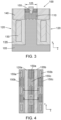
Figure 5 shows schematically a perspective view of a semiconductor device according to an embodiment of the disclosure. Many of the features are similar to those shown inFigure 1 and therefore carry the same reference numerals. Whilst the example shown infigure 1 includes three auxiliary gates within the auxiliary gate structure, the device shown inFigure 5 includes oneauxiliary gate 145 betweenadjacent gate trenches 120. - It will be understood that the additional features shown in
Figures 5 and6 can be equally applied to the embodiments shown inFigures 1 to 4 . - A
collector layer 450, also referred to as a drain or substrate, is formed under the n-drift region 105. Theconductive region 160 of theauxiliary gate 145 extends above an upper surface of then+ contact region 115 and is electrically connected to agate contact layer 410. In the example shown inFigure 5 , theconductive region 160 is electrically coupled with thegate contact layer 410 using aconductive block 490. Theauxiliary gate 145 and thegate trenches 120 may be electrically connected at an edge of the device through a conducting via, or may be electrically connected laterally by joining theauxiliary gate 145 andgate trench 120 using a conducting layer. - The
source contact 155 extends above an upper surface of then+ contact region 115 and is electrically connected to asource contact layer 420. Aninsulation region 430 is provided in between thegate contact layer 410 and thesource contact layer 420. Thegate contact layer 410 and thesource contact layer 420 may be formed of a conductive material, such as metal. - An
interlayer dielectric 440 is disposed over an upper surface of thegate trenches 120 and then+ contact region 115, is located between the upper surface of thegate trenches 120 and then+ contact region 115 and a lower surface of thegate contact layer 410 and thesource contact layer 420. -
Figure 6 shows schematically a perspective view of an alternative semiconductor device according to an embodiment of the disclosure. Many of the features are similar to those shown inFigure 5 and therefore carry the same reference numerals. - An insulation layer 460 (which may be referred to as a dielectric layer) is disposed over the
gate contact layer 410 and theinsulation region 430. Ametal layer 470 is disposed over theinsulation layer 460. -
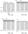
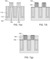
Figures 7(a) to (g) illustrate steps within a method for manufacturing a semiconductor device according to an embodiment of the disclosure. -
Figure 7(a) illustrates the first step of manufacturing the semiconductor device, which is as follows: - (a) Step 1
- A
semiconductor substrate 705 is provided. In an example, the substrate is silicon. The semiconductor substrate may be an epitaxial layer. - A plurality of trenches 720 are etched and filled with an insulating
liner 710conductive region 715. In an example, the conductive region comprises polysilicon and the insulating layer comprises silicon dioxide. - A chemical-mechanical polishing (CMP) process is performed to planarise the surface of the filled trenches 720 and the
semiconductor substrate 705. - A
nitride layer 725 is formed over the mesa region between adjacent gate trenches.
- A
-
Figure 7(b) illustrates the second step of manufacturing the semiconductor device, which is as follows:
(b) Step 2 - A
photoresist layer 730 is deposited over an upper surface of the device. - The
photoresist layer 730 is patterned and subsequently developed such that a mask covers an upper surface of the device, leaving the areas where auxiliary trenches are to be located exposed. -
Figure 7(c) illustrates the third step of manufacturing the semiconductor device, which is as follows:
(c) Step 3 An etch process is performed to remove thenitride layer 725 in regions where thephotoresist 730 is not present, and where the auxiliary trenches are to be located. The etch process stops at or just below an upper surface of thesemiconductor substrate 705. -
Figure 7(d) illustrates the fourth step of manufacturing the semiconductor device, which is as follows:
(d) Step 4 The photoresist layer is removed from the upper surface of the device. -
Figure 7(e) illustrates the fifth step of manufacturing the semiconductor device, which is as follows:
(e) Step 5 A recess etch is performed to remove an upper portion of theconductive region 715 and the insulatingliner 710 from the trenches. The recess etch process removes thesemiconductor substrate 705 in areas not covered by thenitride layer 725, to form theauxiliary trenches 745. The etchant used has an etch selectively such that thenitride layer 725 stops the etchant from removing the remainingsemiconductor substrate 705 in the mesa region. -
Figure 7(f) illustrates the sixth step of manufacturing the semiconductor device, which is as follows:
(f) Step 6 An insulatinglayer 735 is formed over the device on the exposedsubstrate 705, using an oxidation process. In an example, the insulating layer comprises silicon dioxide. -
Figure 7(g) illustrates the seventh step of manufacturing the semiconductor device, which is as follows:
(g) Step 7 - A second
conductive region 740 is deposited over the insulatinglayer 735 and within each of thetrenches 720, 745. In an example, the second conductive region comprises polysilicon. - The second
conductive region 740 is deposited such that an upper surface of the secondconductive region 740 within the gate trenches 720 is below an upper surface of thenitride layer 725. - Whilst
Figures 7(a) to 7(g) illustrate steps within a method of manufacturing a semiconductor device according to an embodiment of the disclosure, they are not exhaustive and the method of manufacturing may include further steps both before and after the steps shown inFigures 7(a) to 7(g) . - The skilled person will understand that in the preceding description and appended claims, positional terms such as 'above', 'overlap', 'under', 'lateral, etc. are made with reference to conceptual illustrations of an apparatus, such as those showing standard cross-sectional perspectives and those shown in the appended drawings. These terms
are used for ease of reference but are not intended to be of limiting nature. These terms are therefore to be understood as referring to a device when in an orientation as shown in the accompanying drawings. - It will be appreciated that all doping polarities mentioned above could be reversed, the resulting devices still being in accordance with embodiments of the present invention.
- In this document, dimensions are provided merely as indicative examples, and are not intended to be limiting.
- Although the disclosure has been described in terms of preferred embodiments as set forth above, it should be understood that these embodiments are illustrative only and that the claims are not limited to those embodiments. Those skilled in the art will be able to make modifications and alternatives in view of the disclosure, which are contemplated as falling within the scope of the appended claims. Each feature disclosed or illustrated in the present specification may be incorporated in the disclosure, whether alone or in any appropriate combination with any other feature disclosed or illustrated herein
-
- 100
- semiconductor device
- 105
- n-drift region
- 110
- p-body region
- 115
- n+ contact region
- 120
- gate trench
- 125
- mesa region
- 130
- trench shield
- 135
- insulation layer
- 140
- gate conductive region
- 145
- auxiliary gate
- 150
- auxiliary gate structure
- 155
- source contact
- 160
- conductive region
- 165
- insulation layer
- 410
- gate contact layer
- 420
- source contact layer
- 430
- insulation region
- 440
- interlayer dielectric
- 450
- collector layer
- 460
- insulation layer
- 470
- metal layer
- 480
- insulation layer
- 490
- conductive block
- 705
- semiconductor substrate
- 710
- insulating liner
- 715
- first conductive region
- 720
- gate trenches
- 725
- nitride layer
- 730
- photoresist layer
- 735
- insulating layer
- 740
- second conductive region
- 745
- auxiliary trench
Claims (20)
- A semiconductor power device comprising:a drift region of a first conductivity type;a body region of a second conductivity type disposed over the drift region, wherein the second conductivity type is opposite to the first conductivity type;at least two gate trench regions in contact with the body region and the drift region, wherein two laterally adjacent gate trench regions are separated by a mesa region;a contact region of a first conductivity type located in the mesa region and disposed over the body region, wherein the contact region has a higher doping concentration compared to the doping concentration of the drift region, and wherein the contact region is in contact with the two adjacent gate trench regions so that, in use, a channel is formed along each gate trench region and within the body region;a source contact disposed over the contact region; andan auxiliary gate region formed within the mesa region.
- The device according to claim 1, wherein the auxiliary gate region extends from a surface of the contact region to a first depth within the device, wherein the first depth is substantially smaller than a total depth of the gate trench regions within the device.
- The device according to claim 1 or 2, wherein each gate trench region comprises a gate conductive region formed in an upper portion of each gate trench region, and a gate insulation layer formed along sidewalls and a lower surface of each gate trench region.
- The device according to claim 3, wherein each gate trench region further comprises a shield electrode in a lower portion of each gate trench region, wherein the shield electrode is insulated from the drift region by the gate insulation layer, and wherein the shield electrode is insulated from the gate electrode by an insulation layer disposed over the shield electrode.
- The device of claim 3 or 4, wherein the upper portion extends to a second depth within the device, wherein the second depth is substantially equal to the depth of the body region within the device.
- The device according to any of claims 3 to 5, wherein the auxiliary gate region extends from a surface of the contact region to a first depth within the device, and wherein the upper portion extends to a second depth within the device, wherein the first depth is equal to or smaller than the second depth.
- The device according to any preceding claim, wherein between two adjacent gate trench regions, the auxiliary gate region comprises a single auxiliary trench gate.
- The device according to any preceding claim, wherein between two adjacent gate trench regions, the auxiliary gate region comprises a plurality of auxiliary trench gates.
- The device according to any preceding claim, wherein between two adjacent gate trench regions, the auxiliary gate region has a width that is equal to or greater than 40% of a width of the mesa region.
- The device according to any preceding claim, wherein the at least two gate trench regions are laterally spaced in a first dimension, wherein current flows in the device in a second dimension substantially transverse to the first dimension, and wherein the gate trench regions extend in a third dimension of the device.
- The device according to claim 10, wherein the source contact is spaced from the auxiliary gate region in the third dimension.
- The device according to claim 11, wherein the device further comprises additional auxiliary gate trench regions located laterally either side of the gate trench regions, and wherein the device further comprises additional source contacts located laterally either side of the gate trench regions.
- The device according to claim 12, wherein the additional auxiliary gate trench regions are in line with the auxiliary gate trench region in the third dimension, and wherein the additional source contacts are in line with the source contact in the third dimension.
- The device according to claim 12, wherein the additional auxiliary gate trench regions are in line with the source contact in in the third dimension, and wherein the additional source contacts are in line with the auxiliary gate trench region in the third dimension.
- The device according to any of claims 12 to 14, further comprising a metal gate contact layer electrically connected to the auxiliary gate trench and the additional auxiliary trench gate regions.
- The device according to claim 15, further comprising a metal source contact layer electrically connected to the source contact.
- The device according to claim 16, wherein the metal gate contact layer and the metal source contact layer are formed in a same plane in the second dimension, and wherein the device further comprises an insulation region located laterally in between the gate contact layer and the metal source contact layer.
- A device according to any preceding claim, wherein the semiconductor device comprises a metal-oxide-semiconductor field-effect transistor (MOSFET).
- A method of manufacturing a semiconductor power device, the method comprising:forming a drift region of a first conductivity type;forming a body region of a second conductivity type over the drift region, wherein the second conductivity type is opposite to the first conductivity type;forming at least two gate trench regions in contact with the body region and the drift region, wherein two laterally adjacent gate trench regions are separated by a mesa region;forming a contact region of a first conductivity type located in the mesa region and disposed over the body region, wherein the contact region has a higher doping concentration compared to a doping concentration of the drift region, and wherein the contact region is in contact with the two adjacent gate trench regions so that, in use, a channel is formed along each gate trench region and within the body region;forming a source contact disposed over the contact region; andforming an auxiliary gate region formed within the mesa region.
- A method of manufacturing a semiconductor device according to claim 19, wherein forming an auxiliary gate region formed within the mesa region comprises:depositing a photoresist layer over a surface of the device;developing a mask in the photoresist layer, such that at least one area within the mesa region is exposed;performing an etching process to form at least one recess defining the auxiliary gate region.
Priority Applications (3)
| Application Number | Priority Date | Filing Date | Title |
|---|---|---|---|
| EP22216888.2A EP4394880A1 (en) | 2022-12-28 | 2022-12-28 | Semiconductor device |
| CN202311819629.4A CN118263315A (en) | 2022-12-28 | 2023-12-27 | Semiconductor device |
| US18/396,934 US20240222496A1 (en) | 2022-12-28 | 2023-12-27 | Semiconductor Device |
Applications Claiming Priority (1)
| Application Number | Priority Date | Filing Date | Title |
|---|---|---|---|
| EP22216888.2A EP4394880A1 (en) | 2022-12-28 | 2022-12-28 | Semiconductor device |
Publications (1)
| Publication Number | Publication Date |
|---|---|
| EP4394880A1 true EP4394880A1 (en) | 2024-07-03 |
Family
ID=84887761
Family Applications (1)
| Application Number | Title | Priority Date | Filing Date |
|---|---|---|---|
| EP22216888.2A Pending EP4394880A1 (en) | 2022-12-28 | 2022-12-28 | Semiconductor device |
Country Status (3)
| Country | Link |
|---|---|
| US (1) | US20240222496A1 (en) |
| EP (1) | EP4394880A1 (en) |
| CN (1) | CN118263315A (en) |
Families Citing this family (1)
| Publication number | Priority date | Publication date | Assignee | Title |
|---|---|---|---|---|
| CN119451143B (en) * | 2024-10-24 | 2025-10-31 | 海信家电集团股份有限公司 | An IGBT structure and semiconductor device |
Citations (4)
| Publication number | Priority date | Publication date | Assignee | Title |
|---|---|---|---|---|
| US20120220092A1 (en) * | 2009-10-21 | 2012-08-30 | Vishay-Siliconix | Method of forming a hybrid split gate simiconductor |
| US20140284711A1 (en) * | 2013-03-22 | 2014-09-25 | Kabushiki Kaisha Toshiba | Semiconductor apparatus |
| US8884364B2 (en) * | 2010-09-09 | 2014-11-11 | Kabushiki Kaisha Toshiba | Semiconductor device with field-plate electrode |
| US20160181417A1 (en) * | 2014-12-22 | 2016-06-23 | Infineon Technologies Ag | Transistor Device with Field-Electrode |
-
2022
- 2022-12-28 EP EP22216888.2A patent/EP4394880A1/en active Pending
-
2023
- 2023-12-27 US US18/396,934 patent/US20240222496A1/en active Pending
- 2023-12-27 CN CN202311819629.4A patent/CN118263315A/en active Pending
Patent Citations (4)
| Publication number | Priority date | Publication date | Assignee | Title |
|---|---|---|---|---|
| US20120220092A1 (en) * | 2009-10-21 | 2012-08-30 | Vishay-Siliconix | Method of forming a hybrid split gate simiconductor |
| US8884364B2 (en) * | 2010-09-09 | 2014-11-11 | Kabushiki Kaisha Toshiba | Semiconductor device with field-plate electrode |
| US20140284711A1 (en) * | 2013-03-22 | 2014-09-25 | Kabushiki Kaisha Toshiba | Semiconductor apparatus |
| US20160181417A1 (en) * | 2014-12-22 | 2016-06-23 | Infineon Technologies Ag | Transistor Device with Field-Electrode |
Also Published As
| Publication number | Publication date |
|---|---|
| CN118263315A (en) | 2024-06-28 |
| US20240222496A1 (en) | 2024-07-04 |
Similar Documents
| Publication | Publication Date | Title |
|---|---|---|
| US8466513B2 (en) | Semiconductor device with enhanced mobility and method | |
| US9842925B2 (en) | Insulated gate semiconductor device having a shield electrode structure and method | |
| EP1528600B1 (en) | Vertical high-voltage transistor | |
| US7427800B2 (en) | Semiconductor device containing dielectrically isolated PN junction for enhanced breakdown characteristics | |
| EP1033759B1 (en) | MOS-gated device having a buried gate and process for forming same | |
| EP1689001B1 (en) | High-voltage field-effect transistor | |
| US8907394B2 (en) | Insulated gate semiconductor device having shield electrode structure | |
| US6798020B2 (en) | High-voltage lateral transistor with a multi-layered extended drain structure | |
| TWI591789B (en) | Method for fabricating an insulated gate semiconductor device having a shield electrode structure | |
| US8237195B2 (en) | Power MOSFET having a strained channel in a semiconductor heterostructure on metal substrate | |
| EP2270843A2 (en) | Method of making a high-voltage insulated gate transistor | |
| US20020175412A1 (en) | Process for forming MOS-gated power device having segmented trench and extended doping zone | |
| EP1054451A2 (en) | MOS-gated power device having extended trench and doping zone and process for forming same | |
| US20150318361A1 (en) | Method for Forming a Transistor Device having a Field Electrode | |
| US20240222496A1 (en) | Semiconductor Device | |
| EP4391073A1 (en) | Nonlinear gate vertical transistor |
Legal Events
| Date | Code | Title | Description |
|---|---|---|---|
| PUAI | Public reference made under article 153(3) epc to a published international application that has entered the european phase |
Free format text: ORIGINAL CODE: 0009012 |
|
| STAA | Information on the status of an ep patent application or granted ep patent |
Free format text: STATUS: THE APPLICATION HAS BEEN PUBLISHED |
|
| AK | Designated contracting states |
Kind code of ref document: A1 Designated state(s): AL AT BE BG CH CY CZ DE DK EE ES FI FR GB GR HR HU IE IS IT LI LT LU LV MC ME MK MT NL NO PL PT RO RS SE SI SK SM TR |
|
| STAA | Information on the status of an ep patent application or granted ep patent |
Free format text: STATUS: REQUEST FOR EXAMINATION WAS MADE |
|
| 17P | Request for examination filed |
Effective date: 20250103 |