EP4394840A2 - Fiber fabry-perot cavity laser phase plate for charged particle microscopy - Google Patents
Fiber fabry-perot cavity laser phase plate for charged particle microscopy Download PDFInfo
- Publication number
- EP4394840A2 EP4394840A2 EP23215453.4A EP23215453A EP4394840A2 EP 4394840 A2 EP4394840 A2 EP 4394840A2 EP 23215453 A EP23215453 A EP 23215453A EP 4394840 A2 EP4394840 A2 EP 4394840A2
- Authority
- EP
- European Patent Office
- Prior art keywords
- region
- charged particle
- fiber assembly
- fiber
- speculum
- Prior art date
- Legal status (The legal status is an assumption and is not a legal conclusion. Google has not performed a legal analysis and makes no representation as to the accuracy of the status listed.)
- Pending
Links
- 239000000835 fiber Substances 0.000 title claims abstract description 99
- 239000002245 particle Substances 0.000 title claims abstract description 76
- 238000000386 microscopy Methods 0.000 title claims abstract description 29
- 125000006850 spacer group Chemical group 0.000 claims abstract description 20
- 239000000758 substrate Substances 0.000 claims abstract description 15
- 230000003287 optical effect Effects 0.000 claims abstract description 11
- 238000004891 communication Methods 0.000 claims abstract description 5
- 238000000034 method Methods 0.000 claims description 13
- 239000011248 coating agent Substances 0.000 claims description 6
- 238000000576 coating method Methods 0.000 claims description 6
- 230000003993 interaction Effects 0.000 claims description 5
- 210000004872 soft tissue Anatomy 0.000 claims description 2
- VYPSYNLAJGMNEJ-UHFFFAOYSA-N Silicium dioxide Chemical compound O=[Si]=O VYPSYNLAJGMNEJ-UHFFFAOYSA-N 0.000 description 16
- 238000005253 cladding Methods 0.000 description 14
- 238000010894 electron beam technology Methods 0.000 description 12
- 238000003384 imaging method Methods 0.000 description 11
- 230000005540 biological transmission Effects 0.000 description 10
- 239000000463 material Substances 0.000 description 10
- 239000011521 glass Substances 0.000 description 8
- 229920001410 Microfiber Polymers 0.000 description 6
- 230000000712 assembly Effects 0.000 description 6
- 238000000429 assembly Methods 0.000 description 6
- 239000010432 diamond Substances 0.000 description 6
- 229910003460 diamond Inorganic materials 0.000 description 6
- 239000003658 microfiber Substances 0.000 description 6
- 238000004458 analytical method Methods 0.000 description 4
- 230000008878 coupling Effects 0.000 description 4
- 238000010168 coupling process Methods 0.000 description 4
- 238000005859 coupling reaction Methods 0.000 description 4
- 230000007423 decrease Effects 0.000 description 4
- 230000004907 flux Effects 0.000 description 4
- 239000007789 gas Substances 0.000 description 4
- 230000006872 improvement Effects 0.000 description 4
- 230000033001 locomotion Effects 0.000 description 4
- 229920000642 polymer Polymers 0.000 description 4
- 239000010453 quartz Substances 0.000 description 4
- 239000000377 silicon dioxide Substances 0.000 description 4
- 229910052814 silicon oxide Inorganic materials 0.000 description 4
- 239000002775 capsule Substances 0.000 description 3
- 230000006870 function Effects 0.000 description 3
- 230000005855 radiation Effects 0.000 description 3
- GWEVSGVZZGPLCZ-UHFFFAOYSA-N Titan oxide Chemical compound O=[Ti]=O GWEVSGVZZGPLCZ-UHFFFAOYSA-N 0.000 description 2
- 238000002679 ablation Methods 0.000 description 2
- 239000000853 adhesive Substances 0.000 description 2
- 230000001070 adhesive effect Effects 0.000 description 2
- 230000003247 decreasing effect Effects 0.000 description 2
- 230000001419 dependent effect Effects 0.000 description 2
- 238000002149 energy-dispersive X-ray emission spectroscopy Methods 0.000 description 2
- 238000005516 engineering process Methods 0.000 description 2
- 238000000407 epitaxy Methods 0.000 description 2
- 238000005286 illumination Methods 0.000 description 2
- 239000000203 mixture Substances 0.000 description 2
- 230000008569 process Effects 0.000 description 2
- 238000002310 reflectometry Methods 0.000 description 2
- 238000002834 transmittance Methods 0.000 description 2
- 238000010521 absorption reaction Methods 0.000 description 1
- 230000009471 action Effects 0.000 description 1
- 238000005136 cathodoluminescence Methods 0.000 description 1
- 230000008859 change Effects 0.000 description 1
- 239000002131 composite material Substances 0.000 description 1
- 238000001816 cooling Methods 0.000 description 1
- 230000000694 effects Effects 0.000 description 1
- 238000005430 electron energy loss spectroscopy Methods 0.000 description 1
- 238000001493 electron microscopy Methods 0.000 description 1
- 239000012530 fluid Substances 0.000 description 1
- 239000011261 inert gas Substances 0.000 description 1
- 150000002500 ions Chemical class 0.000 description 1
- 239000011159 matrix material Substances 0.000 description 1
- 230000007246 mechanism Effects 0.000 description 1
- 238000010248 power generation Methods 0.000 description 1
- 239000004065 semiconductor Substances 0.000 description 1
- 230000003595 spectral effect Effects 0.000 description 1
- 230000003068 static effect Effects 0.000 description 1
- 230000007704 transition Effects 0.000 description 1
- 238000004627 transmission electron microscopy Methods 0.000 description 1
Images



Classifications
-
- H—ELECTRICITY
- H01—ELECTRIC ELEMENTS
- H01J—ELECTRIC DISCHARGE TUBES OR DISCHARGE LAMPS
- H01J37/00—Discharge tubes with provision for introducing objects or material to be exposed to the discharge, e.g. for the purpose of examination or processing thereof
- H01J37/02—Details
- H01J37/22—Optical, image processing or photographic arrangements associated with the tube
- H01J37/226—Optical arrangements for illuminating the object; optical arrangements for collecting light from the object
-
- H—ELECTRICITY
- H01—ELECTRIC ELEMENTS
- H01J—ELECTRIC DISCHARGE TUBES OR DISCHARGE LAMPS
- H01J37/00—Discharge tubes with provision for introducing objects or material to be exposed to the discharge, e.g. for the purpose of examination or processing thereof
- H01J37/02—Details
- H01J37/22—Optical, image processing or photographic arrangements associated with the tube
-
- H—ELECTRICITY
- H01—ELECTRIC ELEMENTS
- H01J—ELECTRIC DISCHARGE TUBES OR DISCHARGE LAMPS
- H01J37/00—Discharge tubes with provision for introducing objects or material to be exposed to the discharge, e.g. for the purpose of examination or processing thereof
- H01J37/02—Details
- H01J37/22—Optical, image processing or photographic arrangements associated with the tube
- H01J37/222—Image processing arrangements associated with the tube
-
- G—PHYSICS
- G01—MEASURING; TESTING
- G01N—INVESTIGATING OR ANALYSING MATERIALS BY DETERMINING THEIR CHEMICAL OR PHYSICAL PROPERTIES
- G01N23/00—Investigating or analysing materials by the use of wave or particle radiation, e.g. X-rays or neutrons, not covered by groups G01N3/00 – G01N17/00, G01N21/00 or G01N22/00
- G01N23/20—Investigating or analysing materials by the use of wave or particle radiation, e.g. X-rays or neutrons, not covered by groups G01N3/00 – G01N17/00, G01N21/00 or G01N22/00 by using diffraction of the radiation by the materials, e.g. for investigating crystal structure; by using scattering of the radiation by the materials, e.g. for investigating non-crystalline materials; by using reflection of the radiation by the materials
- G01N23/203—Measuring back scattering
-
- G—PHYSICS
- G01—MEASURING; TESTING
- G01N—INVESTIGATING OR ANALYSING MATERIALS BY DETERMINING THEIR CHEMICAL OR PHYSICAL PROPERTIES
- G01N23/00—Investigating or analysing materials by the use of wave or particle radiation, e.g. X-rays or neutrons, not covered by groups G01N3/00 – G01N17/00, G01N21/00 or G01N22/00
- G01N23/22—Investigating or analysing materials by the use of wave or particle radiation, e.g. X-rays or neutrons, not covered by groups G01N3/00 – G01N17/00, G01N21/00 or G01N22/00 by measuring secondary emission from the material
- G01N23/225—Investigating or analysing materials by the use of wave or particle radiation, e.g. X-rays or neutrons, not covered by groups G01N3/00 – G01N17/00, G01N21/00 or G01N22/00 by measuring secondary emission from the material using electron or ion
-
- H—ELECTRICITY
- H01—ELECTRIC ELEMENTS
- H01J—ELECTRIC DISCHARGE TUBES OR DISCHARGE LAMPS
- H01J37/00—Discharge tubes with provision for introducing objects or material to be exposed to the discharge, e.g. for the purpose of examination or processing thereof
- H01J37/02—Details
- H01J37/04—Arrangements of electrodes and associated parts for generating or controlling the discharge, e.g. electron-optical arrangement or ion-optical arrangement
- H01J37/10—Lenses
- H01J37/14—Lenses magnetic
-
- H—ELECTRICITY
- H01—ELECTRIC ELEMENTS
- H01J—ELECTRIC DISCHARGE TUBES OR DISCHARGE LAMPS
- H01J37/00—Discharge tubes with provision for introducing objects or material to be exposed to the discharge, e.g. for the purpose of examination or processing thereof
- H01J37/02—Details
- H01J37/20—Means for supporting or positioning the object or the material; Means for adjusting diaphragms or lenses associated with the support
-
- H—ELECTRICITY
- H01—ELECTRIC ELEMENTS
- H01J—ELECTRIC DISCHARGE TUBES OR DISCHARGE LAMPS
- H01J37/00—Discharge tubes with provision for introducing objects or material to be exposed to the discharge, e.g. for the purpose of examination or processing thereof
- H01J37/26—Electron or ion microscopes; Electron or ion diffraction tubes
- H01J37/261—Details
- H01J37/263—Contrast, resolution or power of penetration
-
- H—ELECTRICITY
- H01—ELECTRIC ELEMENTS
- H01J—ELECTRIC DISCHARGE TUBES OR DISCHARGE LAMPS
- H01J37/00—Discharge tubes with provision for introducing objects or material to be exposed to the discharge, e.g. for the purpose of examination or processing thereof
- H01J37/26—Electron or ion microscopes; Electron or ion diffraction tubes
- H01J37/28—Electron or ion microscopes; Electron or ion diffraction tubes with scanning beams
-
- H—ELECTRICITY
- H01—ELECTRIC ELEMENTS
- H01S—DEVICES USING THE PROCESS OF LIGHT AMPLIFICATION BY STIMULATED EMISSION OF RADIATION [LASER] TO AMPLIFY OR GENERATE LIGHT; DEVICES USING STIMULATED EMISSION OF ELECTROMAGNETIC RADIATION IN WAVE RANGES OTHER THAN OPTICAL
- H01S3/00—Lasers, i.e. devices using stimulated emission of electromagnetic radiation in the infrared, visible or ultraviolet wave range
- H01S3/02—Constructional details
- H01S3/04—Arrangements for thermal management
- H01S3/0405—Conductive cooling, e.g. by heat sinks or thermo-electric elements
-
- H—ELECTRICITY
- H01—ELECTRIC ELEMENTS
- H01S—DEVICES USING THE PROCESS OF LIGHT AMPLIFICATION BY STIMULATED EMISSION OF RADIATION [LASER] TO AMPLIFY OR GENERATE LIGHT; DEVICES USING STIMULATED EMISSION OF ELECTROMAGNETIC RADIATION IN WAVE RANGES OTHER THAN OPTICAL
- H01S3/00—Lasers, i.e. devices using stimulated emission of electromagnetic radiation in the infrared, visible or ultraviolet wave range
- H01S3/02—Constructional details
- H01S3/04—Arrangements for thermal management
- H01S3/042—Arrangements for thermal management for solid state lasers
-
- H—ELECTRICITY
- H01—ELECTRIC ELEMENTS
- H01S—DEVICES USING THE PROCESS OF LIGHT AMPLIFICATION BY STIMULATED EMISSION OF RADIATION [LASER] TO AMPLIFY OR GENERATE LIGHT; DEVICES USING STIMULATED EMISSION OF ELECTROMAGNETIC RADIATION IN WAVE RANGES OTHER THAN OPTICAL
- H01S3/00—Lasers, i.e. devices using stimulated emission of electromagnetic radiation in the infrared, visible or ultraviolet wave range
- H01S3/05—Construction or shape of optical resonators; Accommodation of active medium therein; Shape of active medium
- H01S3/06—Construction or shape of active medium
- H01S3/063—Waveguide lasers, i.e. whereby the dimensions of the waveguide are of the order of the light wavelength
- H01S3/067—Fibre lasers
- H01S3/06708—Constructional details of the fibre, e.g. compositions, cross-section, shape or tapering
-
- H—ELECTRICITY
- H01—ELECTRIC ELEMENTS
- H01S—DEVICES USING THE PROCESS OF LIGHT AMPLIFICATION BY STIMULATED EMISSION OF RADIATION [LASER] TO AMPLIFY OR GENERATE LIGHT; DEVICES USING STIMULATED EMISSION OF ELECTROMAGNETIC RADIATION IN WAVE RANGES OTHER THAN OPTICAL
- H01S3/00—Lasers, i.e. devices using stimulated emission of electromagnetic radiation in the infrared, visible or ultraviolet wave range
- H01S3/05—Construction or shape of optical resonators; Accommodation of active medium therein; Shape of active medium
- H01S3/08—Construction or shape of optical resonators or components thereof
-
- G—PHYSICS
- G01—MEASURING; TESTING
- G01N—INVESTIGATING OR ANALYSING MATERIALS BY DETERMINING THEIR CHEMICAL OR PHYSICAL PROPERTIES
- G01N2223/00—Investigating materials by wave or particle radiation
- G01N2223/40—Imaging
- G01N2223/418—Imaging electron microscope
-
- G—PHYSICS
- G01—MEASURING; TESTING
- G01N—INVESTIGATING OR ANALYSING MATERIALS BY DETERMINING THEIR CHEMICAL OR PHYSICAL PROPERTIES
- G01N33/00—Investigating or analysing materials by specific methods not covered by groups G01N1/00 - G01N31/00
- G01N33/48—Biological material, e.g. blood, urine; Haemocytometers
- G01N33/483—Physical analysis of biological material
- G01N33/4833—Physical analysis of biological material of solid biological material, e.g. tissue samples, cell cultures
-
- H—ELECTRICITY
- H01—ELECTRIC ELEMENTS
- H01J—ELECTRIC DISCHARGE TUBES OR DISCHARGE LAMPS
- H01J2237/00—Discharge tubes exposing object to beam, e.g. for analysis treatment, etching, imaging
- H01J2237/004—Charge control of objects or beams
- H01J2237/0041—Neutralising arrangements
-
- H—ELECTRICITY
- H01—ELECTRIC ELEMENTS
- H01J—ELECTRIC DISCHARGE TUBES OR DISCHARGE LAMPS
- H01J2237/00—Discharge tubes exposing object to beam, e.g. for analysis treatment, etching, imaging
- H01J2237/26—Electron or ion microscopes
- H01J2237/2614—Holography or phase contrast, phase related imaging in general, e.g. phase plates
-
- H—ELECTRICITY
- H01—ELECTRIC ELEMENTS
- H01J—ELECTRIC DISCHARGE TUBES OR DISCHARGE LAMPS
- H01J2237/00—Discharge tubes exposing object to beam, e.g. for analysis treatment, etching, imaging
- H01J2237/26—Electron or ion microscopes
- H01J2237/262—Non-scanning techniques
-
- H—ELECTRICITY
- H01—ELECTRIC ELEMENTS
- H01J—ELECTRIC DISCHARGE TUBES OR DISCHARGE LAMPS
- H01J2237/00—Discharge tubes exposing object to beam, e.g. for analysis treatment, etching, imaging
- H01J2237/26—Electron or ion microscopes
- H01J2237/28—Scanning microscopes
- H01J2237/2802—Transmission microscopes
Definitions
- the disclosed technology relates to the field of fiber Fabry-Perot Cavity laser phase plates for charged particle microscopy systems.
- Phase plates for charged particle microscopy can boost image contrast of microscopy specimens, which can be particularly useful for specimens with low intrinsic contrasts, such as specimens typically found in cryo-electron microscopy (cryo-EM), soft matter in material sciences, and thin lamellae in semiconductors.
- Phase plates can be incorporated into the microscopy system to boost the contrast of microscopy specimens, which can lower the required dose to record an image and also mitigate potential irradiation damage to the specimen.
- the enhanced image contrast can also provide for faster image acquisition.
- Existing phase plates can have form factors and/or power consumptions that limit their usage. Accordingly, there is a long-felt need in the field for improved phase plates.
- the present disclosure provides a micro Fabry-Perot laser cavity for charged particle microscopy, comprising: a first fiber assembly and a second fiber assembly, wherein each of the first fiber and the second fiber assembly comprises: an entrance region comprising a single-mode fiber; a spacer region comprising a multimode fiber or a transparent substrate; a convergence region comprising a gradient index fiber or gradient index lens; and a speculum region comprising a multimode fiber or a transparent substrate, the entrance region, spacer region, the convergence region, and the speculum region being in optical communication with one another, and wherein a face of the speculum region of the first fiber assembly faces a face of the speculum region of the second fiber assembly, thereby defining a gap therebetween.
- a charged particle microscope comprising: a charged particle source configured to generate a charged particle beam; a beam column defining a micro Fabry-Perot cavity through which the generated particle beam travels; a magnetic lens defining an upper polepiece and a lower polepiece and housed in the beam column; and a micro Fabry-Perot laser cavity housed in the beam column and positioned at a diffraction focal plane downstream of the sample, with the first diffraction focal plane between the upper polepiece and the lower polepiece (e.g., for parallel illumination of the sample), wherein the micro Fabry-Perot laser cavity is configured to generate a laser beam that travels through the charged particle beam, and optionally the laser beam having an input power of from about 1 ⁇ W to about 1 W, or the micro Fabry-Perot laser cavity defining a gap in the range of from about 1 ⁇ m to about 1000 ⁇ m, the gap configured such that the laser beam passes therethrough.
- a laser phase plate utilizes an optical pondermotive potential to impart the required phase change to the electron beam in a diffraction plane downstream of a TEM sample. Because no material is situated in the electron beam path, which can cause absorption, scattering or energy shifts, the LPP is a nearly ideal implementation of a phase plate for TEM. In a continuous wave LPP implementation, laser light is enhanced and concentrated in an optical cavity to intensities of GW / cm 2 . Macroscopic cavity types have mirrors with radius of curvature ( ROC ) larger than 1 mm and require laser power larger than 10 W.
- ROC radius of curvature
- the present disclosure describes a Fiber Fabry-Perot Cavity (FFPC) to form a LPP that can be arranged in a charged particle microscope, such as transmission electron microscope (TEM).
- the FFPC can include cavity mirrors with a radius of curvature (ROC) smaller than 1 mm, an assembly of fiber optical components for guiding the input beam (e.g., single mode (SM fiber), a cavity mode matching region (e.g., gradient index (GRIN) fiber), and an enhancement of the circulating power between two concave mirrors (e.g., multi-mode (MM) fiber).
- SM fiber single mode
- GRIN gradient index
- MM multi-mode
- the dimensions of the FFPC fiber assembly allow it to fit in the space of a TEM back focal plane, which can be limited to several millimeters between a sample and a lower pole piece of a magnetic lens.
- the improvement of the FFPC performance with respect to macroscopic cavity types allows the use of fiber optical technology at low laser power, and which may include planar light-wave circuits and integrated photonics. Macroscopic cavity types are typically much larger than FFPCs described herein (e.g., 60 times larger in overall cavity length).
- Macroscopic cavities are thus limited in where they can be placed in charged particle microscopy systems, such as a relayed diffraction focal plane or planes downstream of the TEM in a transfer optical lens. Further, macroscopic cavities require much larger power inputs for corresponding intra-cavity laser power generation, for example, 400 times the power input compared to the FFPCs described herein.
- FFPCs described herein can combine several desirable properties in a single microscopic device, like a small mode focus radius, high finesse, efficient coupling, robust fiber assembly and open access to the cavity mode.
- FFPCs significantly improve the cavity parameters such that low power lasers can be used, integrates with fiber optical components and miniaturize dimensions to fit the space of the back focal plane of a TEM of several millimeters.
- the imaging system 160 can be used to focus the transmitted electron flux onto a fluorescent screen 175, which, if desired, can be retracted/withdrawn so as to get it out of the way of axis 130.
- An image (or diffractogram) of (part of) the sample 110 will be formed by imaging system 160 on screen 175, and this can be viewed through viewing port 180.
- spectroscopic apparatus 190 which could be an Electron Energy Loss Spectroscopy (EELS) module, for example.
- EELS Electron Energy Loss Spectroscopy
- spectroscopic apparatus 190 can also be integrated into the imaging system 160.
- the TEM system can include other type of transmission electron microscopy systems such as a scanning transmission electron microscope.
- the TEM system can include another charged particle column such as an ion column.
- FIG. 2 depicts an example microscope column configuration 200 according to the present disclosure.
- the configuration 200 can be, for example, a column of a TEM, such as system 100 as described with reference to FIG. 1 .
- the configuration 200 can be part of imaging system 160, wherein the configuration 200 begins at a plane of the sample 110 of FIG. 1 and extends along electron-optical axis 130.
- a micro FFPC 205 can be positioned in the back focal plane 210 of an objective lens 204.
- the back focal plane 210 can be a distance of a focal length away from the objective lens 204, such that emissions 220 from the charged particle beam interacting with the sample converges at the back focal plane 210.
- the micro FFPC 205 can contain a laser beam 225 which emissions 220 can pass through, which can provide phase shifting to the emissions 220 in relation to unscattered emissions 230.
- the speculum region 320-a, 320-b can define a curved face 325-a, 325-b (e.g., or a portion of the face is curved) that faces the gap.
- the curved face can direct and focus the laser beam to converge at a point in the gap.
- the point can, in some cases, overlap with the beam path of the corresponding microscopy system, for example, electron-optical axis 130 of FIG. 1 .
- the radius of curvature of the face can be dependent on the gap distance between the assemblies 305-a, and 305-b. For example, the radius of curvature can increase with a decrease in gap length between the assemblies 305-a, 305-b.
- the length of the gap can be, e.g., from 1 to 1000 ⁇ m, or from 3 to 750 ⁇ m, or from 5 to 500 ⁇ m, or from 7 to 350 ⁇ m, or from 10 to 250 ⁇ m, or from 20 to 150 ⁇ m.
- FIGs. 4A and 4B depict a micro FFPC 400 according to the present disclosure.
- the micro FFPC 400 can include a first fiber assembly 405-a and a second fiber assembly 405-b.
- Each assembly 405-a, 405-b can include an entrance region 410-a, 410-b, a spacer region 415-a, 415-b, a convergence region 420-a, 420-b, and a speculum region 425-a, 425-b, respectively.
- the spacer region 415-a, 415-b can include a multimode fiber.
- the spacer region 415-a, 415-b can be configured to receive the laser input (e.g., the single-mode input) from the corresponding entrance region 410-a, 410-b, and can generate multimode laser beams along the length of the spacer region 415-a, 415-b.
- the spacer region 415-a, 415-b can facilitate an increase in beam mode propagation through the respective assembly 405-a, 405-b.
- the speculum region 425-a, 425-b can be composed of diamond, silica, quartz, and the like.
- the mirror of the face 430-a, 430-b can include one or more layers of alternating high refractive index material and low refractive index material.
- the mirror can be composed of alternating layers of titanium oxide (TiO 2 ) and silicon oxide (SiO 2 ).
- the mirror can be coupled to the face of the speculum region 425-a, 425-b (e.g., via adhesive, epitaxy, and the like).
- FIG. 5 depicts a micro FFPC 500 according to the present disclosure.
- the micro FFPC 500 can include a first fiber assembly 505-a and a second fiber assembly 505-b.
- Each assembly 505-a, 505-b can include an entrance region 510-a, 510-b, a spacer region 515-a, 515-b, a convergence region 520-a, 520-b, and a speculum region 525-a, 525-b, respectively, which can be entrance regions, convergence regions, spacer regions, and speculum regions discussed with respect to FIGS. 3 , 4A , and 4B .
- the first fiber assembly 505-a and the second fiber assembly 505-b can also include heat sink 535-a and 535-b, respectively.
- the heat sinks 535-a and 535-b can be positioned on an exterior surface of the entrance region 510-a, 510-b, the spacer region 515-a, 515-b, the convergence region 520-a, 520-b, the speculum region 525-a, 525-b, or a combination thereof.
- the heat sinks 535-a, 535-b can circumferentially extend about the axis of propagation for the laser beam.
- An aperture holder such as aperture holder 615, can position a FFPC within the column 600.
- a distal end of the aperture holder 615 can contain a FFPC (e.g., FFPC 200-500 described herein).
- the aperture holder 615 can position the FFPC such that the FFPC is positioned along the electron-optical axis.
- the FFPC can be positioned downstream of the sample, but in some cases can also be positioned between the upper polepiece 605 and the lower polepiece 610.
- the FFPC can be positioned at a back focal plane, such as a back focal plane of a lens 620.
- a laser beam can be generated.
- the laser beam can pass through the FFPC, and cross the electron-optical axis of the microscopy system.
- an electron beam can be generated.
- the electron beam can be generated for example, by an electron source of the microscopy system.
- the electron beam can travel along the electron-optical beam, pass through a sample plane, and interact with the laser beam traveling from the FFPC.
- electron emissions can be captured.
- the electron emissions can result from the emissions interacting with the laser beam. In some cases, the electron emissions also interact with a sample of the microscopy system prior to the interaction with the laser beam.
- the emissions can be captured by a detector, such as by camera 165 of FIG. 1 , or detector 245 of FIG. 2 .
- micro Fabry-Perot laser cavity of any one of Embodiments 1 to 5, wherein the face of the speculum region of each of the first fiber assembly and the second fiber assembly comprises a mirror.
- a method comprising: generating, by a charged particle microscope, a charged electron beam, wherein the charged beam travels through a beam column of the charged particle microscope; generating, by a micro Fabry-Perot laser cavity positioned between an upper polepiece and a lower polepiece of the beam column, in the back focal plane of a sample, a laser beam, wherein a portion the charged particle beam propagates through the laser beam and interacts with the laser beam in the beam column; and capturing, by a charged particle detector of the charged particle microscope, a charged particle image resulting from the interaction.
- Embodiment 13 wherein the charged particle beam further interacts with a sample positioned in the beam column of the charged particle microscope.
- a charged particle microscope comprising: a charged particle source configured to generate a charged particle beam; a beam column defining a micro Fabry-Perot cavity through which the generated particle beam travels; a magnetic lens defining an upper polepiece and a lower polepiece and housed in the beam column; and a micro Fabry-Perot laser cavity housed in the beam column and positioned between the upper polepiece and the lower polepiece, wherein the micro Fabry-Perot laser cavity is configured to generate a laser beam that travels through the charged particle beam, and optionally the laser beam having an input power of from about 1 ⁇ W to about 1 W, or the micro Fabry-Perot laser cavity defining a gap in the range of from about 1 ⁇ m to about 1000 ⁇ m, the gap configured such that the laser beam passes therethrough, or both (a) and (b).
- the length of the gap can be, e.g., from 1 to 1000 ⁇ m, or from 3 to 750 ⁇ m, or from 5 to 500 ⁇ m, or from 7 to 350 ⁇ m, or from 10 to 250 ⁇ m, or from 20 to 150 ⁇ m.
- the charged particle microscope of Embodiment 17 further comprising a sample holder defining a speculum end, wherein the speculum end is configured to hold a sample and be positioned (i) between the upper polepiece and the lower polepiece, and (ii) in a travel path of the charged particle beam.
- micro Fabry-Perot laser cavity is further configured to be positioned between the speculum end of the sample holder and the lower polepiece.
Landscapes
- Physics & Mathematics (AREA)
- Chemical & Material Sciences (AREA)
- Analytical Chemistry (AREA)
- Electromagnetism (AREA)
- Engineering & Computer Science (AREA)
- Plasma & Fusion (AREA)
- Optics & Photonics (AREA)
- General Health & Medical Sciences (AREA)
- Health & Medical Sciences (AREA)
- Life Sciences & Earth Sciences (AREA)
- Biochemistry (AREA)
- General Physics & Mathematics (AREA)
- Immunology (AREA)
- Pathology (AREA)
- Crystallography & Structural Chemistry (AREA)
- Computer Vision & Pattern Recognition (AREA)
- Microscoopes, Condenser (AREA)
Abstract
Description
- The disclosed technology relates to the field of fiber Fabry-Perot Cavity laser phase plates for charged particle microscopy systems.
- Phase plates for charged particle microscopy can boost image contrast of microscopy specimens, which can be particularly useful for specimens with low intrinsic contrasts, such as specimens typically found in cryo-electron microscopy (cryo-EM), soft matter in material sciences, and thin lamellae in semiconductors. Phase plates can be incorporated into the microscopy system to boost the contrast of microscopy specimens, which can lower the required dose to record an image and also mitigate potential irradiation damage to the specimen. In some cases, the enhanced image contrast can also provide for faster image acquisition. Existing phase plates, however, can have form factors and/or power consumptions that limit their usage. Accordingly, there is a long-felt need in the field for improved phase plates.
- In meeting the described long-felt needs, the present disclosure provides novel and inventive Fiber Fabry-Perot Cavity laser phase plates for charged particle microscopy.
- In one aspect, the present disclosure provides a micro Fabry-Perot laser cavity for charged particle microscopy, comprising: a first fiber assembly and a second fiber assembly, wherein each of the first fiber and the second fiber assembly comprises: an entrance region comprising a single-mode fiber; a spacer region comprising a multimode fiber or a transparent substrate; a convergence region comprising a gradient index fiber or gradient index lens; and a speculum region comprising a multimode fiber or a transparent substrate, the entrance region, spacer region, the convergence region, and the speculum region being in optical communication with one another, and wherein a face of the speculum region of the first fiber assembly faces a face of the speculum region of the second fiber assembly, thereby defining a gap therebetween.
- Also provided is a method, comprising: generating, by a charged particle microscope, a charged electron beam, wherein the charged beam travels through a beam column of the charged particle microscope; generating, by a micro Fabry-Perot laser cavity positioned at a diffraction focal plane downstream of the sample, with the first diffraction plane between an upper polepiece and a lower polepiece of the beam column (e.g., for parallel illumination of the sample), in the back focal plane of a sample, a laser beam, wherein a portion the charged particle beam propagates through the laser beam and interacts with the laser beam in the beam column; and capturing, by a charged particle detector of the charged particle microscope, a charged particle image resulting from the interaction.
- Further provided is a charged particle microscope, comprising: a charged particle source configured to generate a charged particle beam; a beam column defining a micro Fabry-Perot cavity through which the generated particle beam travels; a magnetic lens defining an upper polepiece and a lower polepiece and housed in the beam column; and a micro Fabry-Perot laser cavity housed in the beam column and positioned at a diffraction focal plane downstream of the sample, with the first diffraction focal plane between the upper polepiece and the lower polepiece (e.g., for parallel illumination of the sample), wherein the micro Fabry-Perot laser cavity is configured to generate a laser beam that travels through the charged particle beam, and optionally the laser beam having an input power of from about 1 µW to about 1 W, or the micro Fabry-Perot laser cavity defining a gap in the range of from about 1 µm to about 1000 µm, the gap configured such that the laser beam passes therethrough.
Further aspects of the present disclosure as set forth in the following numbered clauses:- - Clause 1 A charged particle microscope, comprising:
- a charged particle source configured to generate a charged particle beam;
- a beam column defining a micro Fabry-Perot cavity through which the charged particle beam travels;
- a magnetic lens defining an upper polepiece and a lower polepiece and housed in the beam column; and
- a micro Fabry-Perot laser cavity housed in the beam column and positioned between the upper polepiece and the lower polepiece,
- wherein the micro Fabry-Perot laser cavity is configured to generate a laser beam that travels through the charged particle beam, and optionally
- (a) the laser beam having an input power of from about 1 µW to about 1 W, or
- (b) the micro Fabry-Perot laser cavity defining a gap in a range of from about 1 µm to about 1000 µm, the gap configured such that the laser beam passes therethrough, or
- (c) both (a) and (b).
- Clause 2. The charged particle microscope of clause 1,, further comprising a sample holder defining a speculum end, wherein the speculum end is configured to hold a sample and be positioned (i) between the upper polepiece and the lower polepiece, and (ii) in a travel path of the charged particle beam.
- Clause 3. The charged particle microscope of clause 2, wherein the micro Fabry-Perot laser cavity is further configured to be positioned between the speculum end of the sample holder and the lower polepiece.
- Clause 4. The charged particle microscope of clause 1, further comprising a laser cavity holder defining a speculum end, wherein the speculum end of the micro Fabry-Perot laser cavity is (i) configured to hold the micro Fabry-Perot laser cavity, and (ii) positioned in a travel path of the charged particle beam.
- For the purpose of illustrating the invention, there is shown in the drawings a form that is presently preferred; it being understood, however, that this invention is not limited to the precise arrangements and instrumentalities shown.
-
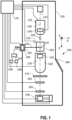
FIG. 1 depicts a microscopy system capable of incorporating micro fiber Fabry-Perot Cavity laser phase plates of the present disclosure. -
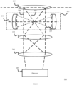
FIG. 2 depicts a microscope column configuration incorporating a micro fiber Fabry-Perot Cavity laser phase plate according to the present disclosure. -
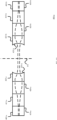
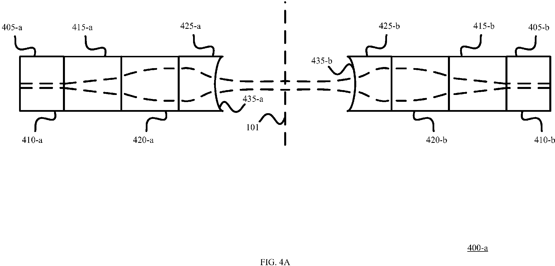
FIGs. 3 ,4A , and4B depict micro fiber Fabry-Perot Cavity laser phase plates according to the present disclosure. -
FIG. 5 depicts an assembly of cavity mirrors and heatsinks for micro fiber Fabry-Perot Cavity laser phase plates according to the present disclosure. -
FIG. 6 depicts a microscope column incorporating a micro fiber Fabry-Perot Cavity laser phase plate according to the present disclosure. -
FIG. 7 depicts a process flow for utilizing a microscopy system having a micro fiber Fabry-Perot Cavity laser phase plate according to the present disclosure. - The present disclosure may be understood more readily by reference to the following detailed description taken in connection with the accompanying figures and examples, which form a part of this disclosure. It is to be understood that this invention is not limited to the specific devices, methods, applications, conditions or parameters described and/or shown herein, and that the terminology used herein is for the purpose of describing particular embodiments by way of example only and is not intended to be limiting of the claimed invention. Also, as used in the specification including the appended claims, the singular forms "a," "an," and "the" include the plural, and reference to a particular numerical value includes at least that particular value, unless the context clearly dictates otherwise. The term "plurality," as used herein, means more than one. When a range of values is expressed, another embodiment includes from the one particular value and/or to the other particular value. Similarly, when values are expressed as approximations, by use of the antecedent "about," it will be understood that the particular value forms another embodiment. All ranges are inclusive and combinable, and it should be understood that steps can be performed in any order. Any documents cited herein are incorporated by reference in their entireties for any and all purposes.
- It is to be appreciated that certain features of the invention which are, for clarity, described herein in the context of separate embodiments, can also be provided in combination in a single embodiment. Conversely, various features of the invention that are, for brevity, described in the context of a single embodiment, can also be provided separately or in any subcombination. Further, reference to values stated in ranges include each and every value within that range. In addition, the term "comprising" should be understood as having its standard, open-ended meaning, but also as encompassing "consisting" as well. For example, a device that comprises Part A and Part B can include parts in addition to Part A and Part B, but can also be formed only from Part A and Part B.
- A laser phase plate (LPP) utilizes an optical pondermotive potential to impart the required phase change to the electron beam in a diffraction plane downstream of a TEM sample. Because no material is situated in the electron beam path, which can cause absorption, scattering or energy shifts, the LPP is a nearly ideal implementation of a phase plate for TEM. In a continuous wave LPP implementation, laser light is enhanced and concentrated in an optical cavity to intensities of GW/cm2. Macroscopic cavity types have mirrors with radius of curvature (ROC) larger than 1 mm and require laser power larger than 10 W.
- The present disclosure describes a Fiber Fabry-Perot Cavity (FFPC) to form a LPP that can be arranged in a charged particle microscope, such as transmission electron microscope (TEM). The FFPC can include cavity mirrors with a radius of curvature (ROC) smaller than 1 mm, an assembly of fiber optical components for guiding the input beam (e.g., single mode (SM fiber), a cavity mode matching region (e.g., gradient index (GRIN) fiber), and an enhancement of the circulating power between two concave mirrors (e.g., multi-mode (MM) fiber). The dimensions of the FFPC fiber assembly, e.g., a diameter of 125 µm, allow it to fit in the space of a TEM back focal plane, which can be limited to several millimeters between a sample and a lower pole piece of a magnetic lens. The improvement of the FFPC performance with respect to macroscopic cavity types allows the use of fiber optical technology at low laser power, and which may include planar light-wave circuits and integrated photonics. Macroscopic cavity types are typically much larger than FFPCs described herein (e.g., 60 times larger in overall cavity length). Macroscopic cavities are thus limited in where they can be placed in charged particle microscopy systems, such as a relayed diffraction focal plane or planes downstream of the TEM in a transfer optical lens. Further, macroscopic cavities require much larger power inputs for corresponding intra-cavity laser power generation, for example, 400 times the power input compared to the FFPCs described herein.
- Disclosed FFPCs can provide nearly three orders of improvement of the intra cavity circulating power with respect to the macroscopic cavity type. This improvement can be utilized to proportionally lower the required laser power from, for example, 20 W to 50 mW. The largest contribution to the reduced power arises from the increased reflectivity of the FFPC, which can act as a counter measure for the decreased cavity length and can positively impact the finesse and power build-up. Similarly, the decreased cavity length can allow for mirrors with smaller ROC, giving rise to a smaller mode focus radius. Such a smaller mode focus radius can also lower the cut-on frequency of the LPP. Table 1 below provides an exemplary and non-limiting comparison between parameters of macroscopic cavities and micro FFPCs described herein.
Table 1. Comparison of macroscopic and FFPC cavity parameters shows the improvement of miniaturization. Step Parameter Macroscopic Microscopic 1 Cavity length [L] 19996.35 µm 399.28 µm 2 ROC 10.00 mm 200.00 µm 3 Reflectivity [R] 138.00 ppm 2.34 ppm 4 Free spectral range [FSR] 7.50 GHz 375.67 GHz 5 Finesse [F] 2.28E + 04 1.34E + 06 6 Linewidth [Δδ] 0.33 MHz 0.28 MHz 7 Quality factor [Qm ]: 8.56E × 08 10.1 × 08 8 Power build-up [BP]: 7.25F × 03 4.27E × 05 9 Mode spacing [Δvtr ] 25.49 MHz 10,137 MHz 10 Mode coupling [ε] 0.90% 0.90% 11 Mode focus radius [w 0] 4.25 µm 1.69 µm 12 Mode mirror radius [w 0] 796.49 µm 39.96 µm 13 Divergence angle [θdiv ] 79.65 mrad 200 mrad 14 Mirror diameter [Droc ] 4141.76 µm 207.81 µm 15 Wavelength [λ] 1064.00 nm 1064.00 nm Intra cavity power [Pc] 1.28 × 10⁵ W 2.03 × 10⁴ W 16 Mode focus power [P0] 450.05 GW/cm2 450.05 GW/cm2 17 Mode mirror power [Pm] 12.83 MW/cm2 808.07 MW/cm2 18 Input power [PI] 19.6 W 52.71 mW - FFPCs described herein can combine several desirable properties in a single microscopic device, like a small mode focus radius, high finesse, efficient coupling, robust fiber assembly and open access to the cavity mode. Advantageously, FFPCs significantly improve the cavity parameters such that low power lasers can be used, integrates with fiber optical components and miniaturize dimensions to fit the space of the back focal plane of a TEM of several millimeters.
- Turning to
FIG. 1, FIG. 1 depicts amicroscopy system 100 configured to use anelectron beam 105 to observe and/or characterize asample 110.microscopy system 100 may acquire an image of thesample 110 using the emissions in the transmission region of themicroscopy system 100. Thus,system 100 can represent a Transmission Electron Microscope (TEM) or a Scanning Transmission Electron Microscope (STEM). - Within a
vacuum enclosure 120, anelectron source 125 can produce thebeam 105 of electrons that propagates along an electron-optical axis 130 and traverses an electron-optical illuminator 135, serving to direct/focus the electrons onto a chosen part of thesample 110 positioned insample chamber 194. In some examples,sample 110 can be, e.g., (locally) thinned/planarized or otherwise processed for analysis, but this is not required in all examples. - Also depicted is a
deflector 140, which can, inter alia, be used to effect scanning motion of thebeam 105. Thesample 110 can be held on asample holder 145 that can be positioned in multiple degrees of freedom by agoniometer 196. For example, thesample 110 can be positioned in a holder capsule of the sample holder that can be moved (inter alia) in the XY plane (see the depicted Cartesian coordinate system; typically, motion parallel to Z and tilt about X/Y will also be possible). Such movement allows different parts of thesample 110 to be illuminated / imaged / inspected by theelectron beam 105 traveling along axis 130 (in the Z direction) (and/or allows scanning motion to be performed, as an alternative to beam scanning). If desired, an optional cooling device (not depicted) can be brought into intimate thermal contact with thesample holder 145, so as to maintain it (and thesample 110 thereupon) at cryogenic temperatures, for example. The holder capsule of the sample holder can be sealable, so that the sample can be transferred into and out of the TEM under vacuum or inert gas. - The sample holder can be in the form of a long rod with two distal ends. The sample holder can include a holder capsule at one distal end wherein the sample, such as the TEM grid, is positioned therein. The sample can be transferred into the sample chamber by inserting one distal end of the sample holder into the TEM column via the load lock. The sample can be imaged or processed by the charged particle beam while being held by the sample holder.
- The
electron beam 105 can interact with thesample 110 in such a manner as to cause various types of stimulated radiation to emanate from thesample 110, including (for example) secondary electrons, backscattered electrons, X-rays and optical radiation (cathodoluminescence). If desired, one or more of these radiation types can be detected with the aid ofanalysis device 155, which might be a combined scintillator/photomultiplier or EDX (Energy-Dispersive X-Ray Spectroscopy) module. However, alternatively or supplementally, one can study electrons that traverse (pass through) thesample 110, exit/emanate from thesample 110, and continue to propagate (substantially, though generally with some deflection/scattering) alongaxis 130. - Such a transmitted electron flux enters an imaging system (projection lens) 160, which can comprise a variety of electrostatic / magnetic lenses, deflectors, correctors (such as stigmators), and the like. In normal (non-scanning) TEM mode, this
imaging system 160 can focus the transmitted electron flux. Various types of analysis apparatuses can be used downstream ofimaging system 160, such as aTEM camera 165. Atcamera 165, the electron flux can form a static image (or diffractogram) that can be processed by controller/processor 170 and displayed on a display device (not depicted), such as a flat panel display, for example. When not required,camera 165 can be retracted/withdrawn so as to get it out of the way ofaxis 130. Alternatively, or additionally, theimaging system 160 can be used to focus the transmitted electron flux onto afluorescent screen 175, which, if desired, can be retracted/withdrawn so as to get it out of the way ofaxis 130. An image (or diffractogram) of (part of) thesample 110 will be formed byimaging system 160 onscreen 175, and this can be viewed through viewingport 180. - An analysis apparatus can also include a
STEM camera 185. An output fromcamera 185 can be recorded as a function of (X,Y) scanning position of thebeam 105 on thesample 110, and an image can be constructed that is a "map" of output fromcamera 185 as a function of X,Y.Camera 185 can include a single pixel with a diameter of e.g. 20 mm, as opposed to the matrix of pixels characteristically present incamera 165. Moreover,camera 185 will generally have a much higher acquisition rate (e.g., 106 points per second) than camera 165 (e.g., 102 - 103 images per second). Once again, when not required,camera 185 can be retracted/withdrawn so as to get it out of the way ofaxis 130. - As an alternative to
imaging using cameras spectroscopic apparatus 190, which could be an Electron Energy Loss Spectroscopy (EELS) module, for example. It should be noted that the order/location ofitems spectroscopic apparatus 190 can also be integrated into theimaging system 160. - The
controller 170 is connected to various illustrated components via control lines (buses). The controller includes at least a processor as well as a non-transitory memory for storing computer readable instructions. By executing the computer readable instructions in the processor, thiscontroller 170 can provide a variety of functions, such as synchronizing actions, providing setpoints, processing signals, performing calculations, and displaying messages/information on a display device (not depicted). The controller can be configured to implement some or all steps of the methods described herein. Thecontroller 170 can be (partially) inside or outside theenclosure 120, and can have a unitary or composite structure, as desired. - The
goniometer 196 can position the sample under the electron beam within a vacuum chamber of the microscope. The vacuum chamber can be asample chamber 194. The sample can be imaged or processed with the charged particle beams in the sample chamber. Thegoniometer 196 can be coupled withenclosure 120. The goniometer can include one or more actuation mechanisms for tilting the sample around one or more tilt axes. - The
goniometer 196 includes aload lock 195 to facilitate the transfer ofsample 110 from external to themicroscope 100 to within the sample chamber. Theload lock 195 can include ingress/egress points for thesample 110 to transition from the external of the TEM to theload lock 195, and from theload lock 195 to the sample chamber of themicroscope system 100. For example, theload lock 195 can include an opening at one end for receiving a sample holder from the external of TEM. The load lock can be sealable from the external environment via one or more O-rings. Similarly, theload lock 195 can also include an opening on another end (e.g. opposite end) for passing the sample held by the sample holder from theload lock 195 to the sample chamber of the microscope. The opening between the load lock and the sample chamber is sealable via a valve. Thus, when thesample 110 is positioned within the load lock 195 (via the sample holder), the environment of load lock can be substantially isolated from sample chamber. - The
goniometer 196 can include agas delivery train 197 to place the chamber into interruptible fluid communication with both a protectingsource 198 and with avacuum pump 199. Theload lock 195 can be coupled with one or more gas sources and pumps via valves for controlling the gas flow into and out of theload lock 195. In one example, the load lock can be fluidically connected to avacuum pump 199 via a first valve and fluidically connected to a protectinggas source 198 via a second valve. The valves can be open or closed by actuation respective actuators controlled by thecontroller 170. - The
system 100 can also include amicro FFPC 191 according to the present disclosure. Themicro FFPC 191 can be positioned along theaxis 130. In some cases, themicro FFPC 191 can be positioned in theimaging system 160, or between theimaging system 160 and thesample 110. A laser can be coupled to themicro FFPC 191 to an external laser source (not shown), and can be configured to receive and transmit a laser emission to intersect theaxis 130. The transmitted laser emission can form a standing wave intersecting theaxis 130, which can interact with emissions generated by theelectron beam 105 along theaxis 130. - The TEM system can include other type of transmission electron microscopy systems such as a scanning transmission electron microscope. In some examples, the TEM system can include another charged particle column such as an ion column.
-
FIG. 2 depicts an examplemicroscope column configuration 200 according to the present disclosure. Theconfiguration 200 can be, for example, a column of a TEM, such assystem 100 as described with reference toFIG. 1 . For example, theconfiguration 200 can be part ofimaging system 160, wherein theconfiguration 200 begins at a plane of thesample 110 ofFIG. 1 and extends along electron-optical axis 130. - A
micro FFPC 205 can be positioned in the backfocal plane 210 of an objective lens 204. The backfocal plane 210 can be a distance of a focal length away from the objective lens 204, such thatemissions 220 from the charged particle beam interacting with the sample converges at the backfocal plane 210. Themicro FFPC 205 can contain alaser beam 225 whichemissions 220 can pass through, which can provide phase shifting to theemissions 220 in relation tounscattered emissions 230. - Due to their large size, macroscopic cavities are limited to being positioned closer to the
detector 245, such as between theprojector lens 240 and thedetector 245, or between theintermediate lens 235 and theprojector lens 240. This area of theconfiguration 200 is typically larger in size (e.g., in diameter of the column), thereby allowing for larger cavities to be present. The micro FFPC, however, is significantly smaller in size, and can therefore be positioned further up the column, and closer to the sample, such as at the back focal plane 210). -
FIG. 3 depicts amicro FFPC 300 according to the present disclosure. Themicro FFPC 300 can include a first fiber assembly 305-a and a second fiber assembly 305-b. Each assembly 305-a, 305-b can include an entrance region 310-a, 310-b, a convergence region 315-a, 315-b, and a speculum region 320-a, 320-b, respectively. - The entrance region 310-a, 310-b can include a single-mode fiber. The entrance region 310-a, 310-b can be configured to receive a laser input, and transfer the laser to the corresponding convergence region 315-a, 315-b. The entrance region 310-a, 310-b can define a core and cladding, where the cladding envelops the core. The core can include a diameter, for example, of between 5 um and 10 um (e.g., with respect to the axis of transmission for the assembly 305-a, 305-b), and the cladding can include a diameter of between 100 um and 150 um. The core can be composed of plastic or glass, and the cladding can be composed of material having an index of refraction lower than that of the core (e.g., glass, polymers, and the like).
- The convergence region 315-a, 315-b can include a gradient index fiber. The convergence region 315-a, 315-b can be configured to receive the laser input (e.g., the single-mode input) from the corresponding entrance region 310-a, 310-b, and can create mode matched laser beams along the length of the convergence region 315-a, 315-b. For example, the convergence region 315-a, 315-b can include a core and cladding. The core can include a refractive index that decreases with increasing radial distance away from the axis of transmission. The varied index of refraction can cause the laser beam to travel in a sinusoidal form along the length of the convergence region 315-a, 315-b. The core of the convergence region 315-a, 315-b can be, e.g., plastic or glass, and the cladding can be composed of material having an index of refraction lower than that of the core (e.g., glass, polymers, and the like). The core can include a diameter between 50 and 250 um, and the cladding can include a diameter between 100 and 500 um.
- The speculum region 320-a, 320-b can include, or form, or be a mirror. For example, the speculum region 320-a, 320-b can be configured to receive the mode matched laser beams, and to transmit the laser beams towards the gap defined by the assemblies 305-a, 305-b. The speculum region 320-a, 320-b can be further configured to reflect laser beams received from the other assembly. For example, speculum region 320-a can be configured to reflect laser beams received from speculum region 320-b, and vice versa. This transmittance and reflectance of laser beams can significantly reduce input power for the laser beam (See, e.g., Table 1). For example, a laser can have an input power of, e.g., about 1 µW to about 1 W, about 10 µW to 0.1 W, about 100 µW to about 0.01 W, and all intermediate values. The speculum region 320-a, 320-b can be composed of a high thermal conductive substrate. In some cases, the speculum region 320-a, 320-b, can be composed of diamond. In some cases, the speculum region 320-a, 320-b can be composed of silica, or quartz.
- The speculum region 320-a, 320-b can define a curved face 325-a, 325-b (e.g., or a portion of the face is curved) that faces the gap. The curved face can direct and focus the laser beam to converge at a point in the gap. The point can, in some cases, overlap with the beam path of the corresponding microscopy system, for example, electron-
optical axis 130 ofFIG. 1 . Further, the radius of curvature of the face can be dependent on the gap distance between the assemblies 305-a, and 305-b. For example, the radius of curvature can increase with a decrease in gap length between the assemblies 305-a, 305-b. As some examples, the length of the gap can be, e.g., from 1 to 1000 µm, or from 3 to 750 µm, or from 5 to 500 µm, or from 7 to 350 µm, or from 10 to 250 µm, or from 20 to 150 µm. - In some cases, the speculum region 320-a, 320-b can include a multimode fiber. In some cases, the curved face 325-a, 325-b can be ablated or etched, such as via thermal ablation, for forming the curved face 325-a, 325-b in the speculum region 320-a, 320-b. In some cases, the mirror can be of a different composition of the speculum region 320-a, 320-b. and can be defined in the face 325-a, 325-b. For example, the speculum region 320-a, 320-b can be composed of diamond, silica, quartz, and the like. The mirror of the face 325-a, 325-b can include one or more layers of alternating high refractive index material and low refractive index material. For example, the mirror can be composed of alternating layers of titanium oxide (TiO2) and silicon oxide (SiO2). In some cases, the speculum region 320-a, 320-b can be composed of a high thermal conductive substrate, with the alternating layers layered on the substrate. In some cases, the mirror can be coupled to the face of the speculum region 320-a, 320-b (e.g., via adhesive, epitaxy, and the like).
- In some cases, the speculum region 320-a, 320-b can include a coupling area that is flush with the corresponding convergence region 315-a, 315-b, such as those depicted in
FIG. 3 . In other cases, the speculum region 320-a, 320-b can further definewall 325 that extends distally away from the face of the speculum region 320-a, 320-b (e.g., along the axis of transmission). Thewall 325 can define a recess which the convergence region 315-a, 315-b can be inserted. An example of the walls are depicted in FIG. 8. The speculum region 320-a, 320-b can include a diameter between 300 um and 700 um. In some cases, the overall length of the micro-FFPC 300 can be between 100 and 200 µm, between 100 and 500 µm, between 50 and 1,000 µm, and the like. -
FIGs. 4A and4B depict amicro FFPC 400 according to the present disclosure. Themicro FFPC 400 can include a first fiber assembly 405-a and a second fiber assembly 405-b. Each assembly 405-a, 405-b can include an entrance region 410-a, 410-b, a spacer region 415-a, 415-b, a convergence region 420-a, 420-b, and a speculum region 425-a, 425-b, respectively. - The entrance region 410-a, 410-b can include a single-mode fiber. The entrance region 410-a, 410-b can be configured to receive a laser input, and transfer the laser to the corresponding spacer region 415-a, 415-b. The entrance region 410-a, 410-b can define a core and cladding, where the cladding envelops the core. The core can include a diameter, for example, from 1 to 1000 µm, or from 3 to 750 µm, or from 5 to 500 µm, or from 7 to 350 µm, or from 10 to 250 µm, or from 20 to 150 µm.
(e.g., with respect to the axis of transmission for the assembly 405-a, 405-b), and the cladding can include a diameter of between 100 um and 150 um. The core can be composed of plastic or glass, and the cladding can be composed of material having an index of refraction lower than that of the core (e.g., glass, polymers, and the like). - The spacer region 415-a, 415-b can include a multimode fiber. The spacer region 415-a, 415-b can be configured to receive the laser input (e.g., the single-mode input) from the corresponding entrance region 410-a, 410-b, and can generate multimode laser beams along the length of the spacer region 415-a, 415-b. The spacer region 415-a, 415-b can facilitate an increase in beam mode propagation through the respective assembly 405-a, 405-b.
- The convergence region 420-a, 420-b can include a gradient index fiber. The convergence region 420-a, 420-b can be configured to receive the laser input (e.g., the single-mode input) from the corresponding spacer region 415-a, 415-b, and can create mode matched laser beams along the length of the convergence region 420-a, 420-b. For example, the convergence region 420-a, 420-b can define a core and cladding. The core can include a refractive index that decreases with increasing radial distance away from the axis of transmission. The varied index of refraction can cause the laser beam to travel in a sinusoidal form along the length of the convergence region 420-a, 420-b. The core of the convergence region 420-a, 420-b can be plastic or glass, and the cladding can be composed of material having an index of refraction lower than that of the core (e.g., glass, polymers, and the like). The core can include a diameter between 50 and 250 um, and the cladding can include a diameter between 100 and 500 um.
- The speculum region 425-a, 425-b can include a mirror. For example, the speculum region 425-a, 425-b can be configured to receive the mode matched laser beams, and to transmit the laser beams towards the gap defined by the assemblies 405-a, 405-b. The speculum region 425-a, 425-b can be further configured to reflect laser beams received from the other assembly. For example, speculum region 425-a can be configured to reflect laser beams received from speculum region 425-b, and vice versa. This transmittance and reflectance of laser beams can significantly reduce input power for the laser beam (See, e.g., Table 1). In some cases, the speculum region 425-a, 425-b, can be composed of diamond. In some cases, the speculum region 425-a, 425-b can be composed of silica, or quartz.
- The speculum region 425-a, 425-b can define a curved face 430-a, 430-b (e.g., or a portion of the face is curved) that faces the gap. The curved face can direct and focus the laser beam to converge at a point in the gap. The point can, in some cases, overlap with the beam path of the corresponding microscopy system, for example, electron-optical axis 1030 of
FIG. 1 . Further, the radius of curvature of the face can be dependent on the gap distance between the assemblies 405-a, and 405-b. For example, the radius of curvature can increase with a decrease in gap length between the assemblies 405-a, 405-b. In some cases, the radius of curvature can be between 200 and 500 um. - The speculum region 425-a, 425-b can be composed of a mirror, or can include a mirror. In some cases, the speculum region 425-a, 425-b can include a multimode fiber. In some cases, the curved face 430-a, 430-b can be ablated or etched, such as via thermal ablation, for forming the curved face 430-a, 430-b in the speculum region 425-a, 425-b. In some cases, the mirror can be of a different composition of the speculum region 425-a, 425-b. and can be defined in the face 430-a, 430-b. For example, the speculum region 425-a, 425-b can be composed of diamond, silica, quartz, and the like. The mirror of the face 430-a, 430-b can include one or more layers of alternating high refractive index material and low refractive index material. For example, the mirror can be composed of alternating layers of titanium oxide (TiO2) and silicon oxide (SiO2). In some cases, the mirror can be coupled to the face of the speculum region 425-a, 425-b (e.g., via adhesive, epitaxy, and the like).
- In some cases, the speculum region 425-a, 425-b can include a coupling area that is flush with the corresponding convergence region 420-a, 420-b, such as those depicted in
FIG. 4 . In other cases, the speculum region 425-a, 425-b can further define a recess which the convergence region 420-a, 420-b can be inserted. An example of the recess is depicted inFIG. 4B . The speculum region 425-a, 425-b can include a diameter between 300 um and 700 um. -
FIG. 5 depicts amicro FFPC 500 according to the present disclosure. Themicro FFPC 500 can include a first fiber assembly 505-a and a second fiber assembly 505-b. Each assembly 505-a, 505-b can include an entrance region 510-a, 510-b, a spacer region 515-a, 515-b, a convergence region 520-a, 520-b, and a speculum region 525-a, 525-b, respectively, which can be entrance regions, convergence regions, spacer regions, and speculum regions discussed with respect toFIGS. 3 ,4A , and4B . - The first fiber assembly 505-a and the second fiber assembly 505-b can also include heat sink 535-a and 535-b, respectively. The heat sinks 535-a and 535-b can be positioned on an exterior surface of the entrance region 510-a, 510-b, the spacer region 515-a, 515-b, the convergence region 520-a, 520-b, the speculum region 525-a, 525-b, or a combination thereof. In some cases, the heat sinks 535-a, 535-b can circumferentially extend about the axis of propagation for the laser beam. The heat sinks 535-a, 535-b can include a section 540-a, 540-b that runs perpendicular to the electron-optical axis 130 (e.g., along the length of the assembly 505-a, 505-b respectively). The heat sinks 535-a, 535-b can also include a section 545-a, 545b that runs parallel to the electron-
optical axis 130. The parallel section 545-a, 545-b can define an edge 550-a, 550-b, for allowing laser emissions from the speculum region 525-a, 525-b to pass to the electron-optical axis 130. In some cases, the edge 550-a, 550-b can be shaped to minimize laser emissions from contacting the heat sink 535-a, 535-b. For example, the face of the speculum region 525-a, 525-b can be curved to converge the laser emissions emitted from the respective speculum region. The edge 550-a, 550-b can be angled to allow for this convergence to occur. -
FIG. 6 depicts amicroscope column 600 according to the present disclosure. Thecolumn 600 can be implemented in a microscopy system, such asmicroscopy system 100 ofFIG. 1 . In some cases, thecolumn 600 can include a part ofimaging system 160. - In some cases, the
column 600 can include magnetic lenses, which can include anupper polepiece 605 and alower polepiece 610. In some cases, a sample plane can be located between theupper polepiece 605 and the lower polepiece 610 (e.g., along the electron-optical axis). Asample holder 625 can position a sample at the sample plane (e.g., by repositioning the distal end containing the sample, of the sample holder 625). - An aperture holder, such as
aperture holder 615, can position a FFPC within thecolumn 600. For example, a distal end of theaperture holder 615 can contain a FFPC (e.g., FFPC 200-500 described herein). Theaperture holder 615 can position the FFPC such that the FFPC is positioned along the electron-optical axis. Additionally, the FFPC can be positioned downstream of the sample, but in some cases can also be positioned between theupper polepiece 605 and thelower polepiece 610. In some cases, the FFPC can be positioned at a back focal plane, such as a back focal plane of alens 620. -
FIG. 7 depicts aprocess 700 for implementing a FFPC according to the present disclosure. AtStep 705, a FFPC can be positioned within a microscopy system. The FFPC can be an example ofFFPC FIGS. 2-5 . In some cases, the FFPC can be positioned within a microscopy system, such asmicroscopy system 100 ofFIG. 1 . In some cases, the FFPC can be positioned within a microscope column, such ascolumn 600 ofFIG. 6 . In some cases, the FFPC can be positioned between upper and lower polepieces of a magnetic lens. In some cases, the FFPC can be positioned downstream of a sample, such as at a back focal plane or diffraction plane of the sample. In some cases, the FFPC can be positioned via an aperture holder of the microscopy system. - At
Step 710, a laser beam can be generated. The laser beam can pass through the FFPC, and cross the electron-optical axis of the microscopy system. AtStep 715, an electron beam can be generated. The electron beam can be generated for example, by an electron source of the microscopy system. The electron beam can travel along the electron-optical beam, pass through a sample plane, and interact with the laser beam traveling from the FFPC. AtStep 720, electron emissions can be captured. The electron emissions can result from the emissions interacting with the laser beam. In some cases, the electron emissions also interact with a sample of the microscopy system prior to the interaction with the laser beam. The emissions can be captured by a detector, such as bycamera 165 ofFIG. 1 , ordetector 245 ofFIG. 2 . - The following embodiments are exemplary only and do not serve to limit the scope of the present disclosure of the appended claims. It should be understood that any part of any one or more Embodiments can be combined with any part of any other one or more Embodiments.
- A micro Fabry-Perot laser cavity for charged particle microscopy, comprising: a first fiber assembly and a second fiber assembly, wherein each of the first fiber and the second fiber assembly comprises: an entrance region comprising a single-mode fiber; a spacer region comprising a multimode fiber or a transparent substrate; a convergence region comprising a gradient index fiber or gradient index lens; and a speculum region comprising a multimode fiber or a transparent substrate, the entrance region, spacer region, the convergence region, and the speculum region being in optical communication with one another, and wherein a face of the speculum region of the first fiber assembly faces a face of the speculum region of the second fiber assembly, thereby defining a gap therebetween.
- The micro Fabry-Perot laser cavity of Embodiment 1, wherein the gradient index fiber or gradient index lens is configured to receive a broadened laser beam diameter from the multimode fiber or transparent substrate in the spacer region and mode match the laser beam to the mirror radiance of curvature in the speculum region and the gap.
- The micro Fabry-Perot laser cavity of any one of Embodiments 1 or 2, wherein a length of the gap comprises between 1 µm and 1000 µm. As some examples, the length of the gap can be, e.g., from 1 to 1000 µm, or from 3 to 750 µm, or from 5 to 500 µm, or from 7 to 350 µm, or from 10 to 250 µm, or from 20 to 150 µm.
- The micro Fabry-Perot laser cavity of any one of Embodiments 1 to 3, wherein the each of the first fiber assembly and the second fiber assembly is configured to transport a laser beam having an input power of from about 1 µW to about 1 W. A laser can have an input power of, e.g., about 1 µW to about 1 W, about 10 µW to 0.1 W, about 100 µW to about 0.01 W, and all intermediate values.
- The micro Fabry-Perot laser cavity of any one of Embodiments 1 to 4, wherein a core diameter of each of the first fiber assembly and the second fiber assembly is in the range of from between about 1 µm and about 1000 µm. As some examples, a core diameter can be, e.g., from 1 to 1000 µm, or from 3 to 750 µm, or from 5 to 500 µm, or from 7 to 350 µm, or from 10 to 250 µm, or from 20 to 150 µm.
- The micro Fabry-Perot laser cavity of any one of Embodiments 1 to 5, wherein the face of the speculum region of each of the first fiber assembly and the second fiber assembly comprises a mirror.
- The micro Fabry-Perot laser cavity of any one of Embodiments 1 to 6, wherein the speculum region for at least one of the first fiber assembly and the second comprises diamond, the diamond optionally comprising a dielectric reflective coating, the dielectric reflective coating optionally comprising at least a first layer and a second layer, the first layer and the second layer having different reflective indices.
- The micro Fabry-Perot laser cavity of any one of Embodiments 1 to 7, wherein the micro Fabry-Perot laser cavity is configured to be positioned in a beam column of a charged particle microscope such that a portion of the charged particle beam of the charged particle microscope passes through the gap of the micro Fabry-Perot laser cavity.
- The micro Fabry-Perot laser cavity of any one of Embodiments 1 to 8, wherein the micro Fabry-Perot laser cavity is configured to be positioned between an upper polepiece of a magnetic lens of the charged particle microscope and a lower polepiece of the magnetic lens of the charged particle microscope.
- The micro Fabry-Perot laser cavity of any one of Embodiments 1 to 9, further comprising a dielectric coating covering at least a portion of the face of the first fiber assembly and the face of the second fiber assembly.
- The micro Fabry-Perot laser cavity of any one of Embodiments 1 to 10, further comprising a thermal sink in contact with the speculum region of at least one of the first fiber assembly and the second fiber assembly.
- The micro Fabry-Perot laser cavity of any one of Embodiments 1 to 11, further comprising an electrical shield positioned in the gap and configured to reduce an electrical charge buildup on the face of the first fiber assembly and the face of the second fiber assembly from a charged beam travelling through the gap.
- A method, comprising: generating, by a charged particle microscope, a charged electron beam, wherein the charged beam travels through a beam column of the charged particle microscope; generating, by a micro Fabry-Perot laser cavity positioned between an upper polepiece and a lower polepiece of the beam column, in the back focal plane of a sample, a laser beam, wherein a portion the charged particle beam propagates through the laser beam and interacts with the laser beam in the beam column; and capturing, by a charged particle detector of the charged particle microscope, a charged particle image resulting from the interaction.
- The method of Embodiment 13, wherein the charged particle beam further interacts with a sample positioned in the beam column of the charged particle microscope.
- The method of any one of Embodiments 13 or 14, wherein the sample comprises a soft tissue sample.
- A method of any one of Embodiments 13 to 15, wherein the charged particle beam is captured as an image.
- A charged particle microscope, comprising: a charged particle source configured to generate a charged particle beam; a beam column defining a micro Fabry-Perot cavity through which the generated particle beam travels; a magnetic lens defining an upper polepiece and a lower polepiece and housed in the beam column; and a micro Fabry-Perot laser cavity housed in the beam column and positioned between the upper polepiece and the lower polepiece, wherein the micro Fabry-Perot laser cavity is configured to generate a laser beam that travels through the charged particle beam, and optionally the laser beam having an input power of from about 1 µW to about 1 W, or the micro Fabry-Perot laser cavity defining a gap in the range of from about 1 µm to about 1000 µm, the gap configured such that the laser beam passes therethrough, or both (a) and (b). The length of the gap can be, e.g., from 1 to 1000 µm, or from 3 to 750 µm, or from 5 to 500 µm, or from 7 to 350 µm, or from 10 to 250 µm, or from 20 to 150 µm.
- The charged particle microscope of Embodiment 17, further comprising a sample holder defining a speculum end, wherein the speculum end is configured to hold a sample and be positioned (i) between the upper polepiece and the lower polepiece, and (ii) in a travel path of the charged particle beam.
- The charged particle microscope of any one of Embodiments 17 or 18, wherein the micro Fabry-Perot laser cavity is further configured to be positioned between the speculum end of the sample holder and the lower polepiece.
- The charged particle microscope of any one of Embodiments 17 to 19, further comprising a laser cavity holder defining a speculum end, wherein the speculum end of the micro Fabry-Perot laser cavity holder is (i) configured to hold the micro Fabry-Perot laser cavity, and (ii) positioned in a travel path of the charged particle beam.
Claims (16)
- A micro Fabry-Perot laser cavity for charged particle microscopy, comprising:
a first fiber assembly and a second fiber assembly, wherein each of the first fiber assembly and the second fiber assembly comprises:an entrance region comprising a single-mode fiber;a spacer region comprising a multimode fiber or a transparent substrate;a convergence region comprising a gradient index fiber or gradient index lens; anda speculum region comprising a multimode fiber or a transparent substrate,the entrance region, spacer region, the convergence region, and the speculum region being in optical communication with one another, andwherein a face of the speculum region of the first fiber assembly faces a face of the speculum region of the second fiber assembly, thereby defining a gap therebetween. - The micro Fabry-Perot laser cavity of claim 1, wherein the gradient index fiber or gradient index lens is configured to receive a broadened laser beam diameter of a laser beam from the multimode fiber or transparent substrate in the spacer region and mode match the laser beam to a mirror radiance of curvature in the speculum region and the gap.
- The micro Fabry-Perot laser cavity of claim 1, wherein a length of the gap comprises between 1 µm and 1000 µm.
- The micro Fabry-Perot laser cavity of claim 1, wherein the each of the first fiber assembly and the second fiber assembly is configured to transport a laser beam having an input power of from about 1 µW to about 1 W.
- The micro Fabry-Perot laser cavity of claim 1, wherein a core diameter of each of the first fiber assembly and the second fiber assembly is in a range of from between about 1 µm and about 1000 µm.
- The micro Fabry-Perot laser cavity of claim 1, wherein the face of the speculum region of each of the first fiber assembly and the second fiber assembly comprises a mirror.
- The micro Fabry-Perot laser cavity of claim 1, wherein the speculum region for at least one of the first fiber assembly and the second fiber assembly comprises a high thermal conductive substrate, the high thermal conductive substrate optionally comprising a dielectric reflective coating, the dielectric reflective coating optionally comprising at least a first layer and a second layer, the first layer and the second layer having different reflective indices.
- The micro Fabry-Perot laser cavity of claim 1, wherein the micro Fabry-Perot laser cavity is configured to be positioned in a column of a charged particle microscope such that a portion of a charged particle beam of the charged particle microscope passes through the gap.
- The micro Fabry-Perot laser cavity of claim 8, wherein the micro Fabry-Perot laser cavity is configured to be positioned at a diffraction focal plane downstream of a sample, wherein the diffraction focal plane is located between an upper polepiece of a magnetic lens of the charged particle microscope and a lower polepiece of the magnetic lens of the charged particle microscope.
- The micro Fabry-Perot laser cavity of claim 1, further comprising a dielectric coating covering at least a portion of the face of the first fiber assembly and the face of the second fiber assembly.
- The micro Fabry-Perot laser cavity of claim 1, further comprising a thermal sink in contact with the speculum region of at least one of the first fiber assembly and the second fiber assembly.
- The micro Fabry-Perot laser cavity of claim 1, further comprising an electrical shield positioned in the gap and configured to reduce an electrical charge buildup on the face of the first fiber assembly and the face of the second fiber assembly from a charged beam travelling through the gap.
- A method, comprising:generating, by a charged particle microscope, a charged particle beam, wherein the charged particle beam travels through a beam column of the charged particle microscope;generating, by a micro Fabry-Perot laser cavity positioned at a back focal plane of the charged particle microscope, a standing wave, wherein a portion of the charged particle beam propagates through the standing wave and experiences an interaction with the standing wave in the beam column; andcapturing, by a charged particle detector of the charged particle microscope, a charged particle image resulting from the interaction.
- The method of claim 13, wherein the charged particle beam further interacts with a sample positioned in the beam column of the charged particle microscope.
- The method of claim 14, wherein the sample comprises a soft tissue sample.
- The method of claim 13, wherein the charged particle beam is captured as an image.
Applications Claiming Priority (1)
| Application Number | Priority Date | Filing Date | Title |
|---|---|---|---|
| US202263436214P | 2022-12-30 | 2022-12-30 |
Publications (2)
| Publication Number | Publication Date |
|---|---|
| EP4394840A2 true EP4394840A2 (en) | 2024-07-03 |
| EP4394840A3 EP4394840A3 (en) | 2024-09-18 |
Family
ID=89167979
Family Applications (1)
| Application Number | Title | Priority Date | Filing Date |
|---|---|---|---|
| EP23215453.4A Pending EP4394840A3 (en) | 2022-12-30 | 2023-12-11 | Fiber fabry-perot cavity laser phase plate for charged particle microscopy |
Country Status (4)
| Country | Link |
|---|---|
| US (1) | US20240222066A1 (en) |
| EP (1) | EP4394840A3 (en) |
| JP (1) | JP2024096079A (en) |
| CN (1) | CN118280796A (en) |
Families Citing this family (1)
| Publication number | Priority date | Publication date | Assignee | Title |
|---|---|---|---|---|
| CN121679848B (en) * | 2026-02-12 | 2026-06-02 | 清华大学 | Open microcavity system and experimental setup under low temperature magnetic field |
Family Cites Families (5)
| Publication number | Priority date | Publication date | Assignee | Title |
|---|---|---|---|---|
| US10395888B2 (en) * | 2017-03-30 | 2019-08-27 | The Regents Of The University Of California | Optical-cavity based ponderomotive phase plate for transmission electron microscopy |
| US10348058B1 (en) * | 2018-01-22 | 2019-07-09 | National Tsing Hua University | Two-dimensional material plasmonic laser |
| WO2019213137A1 (en) * | 2018-04-30 | 2019-11-07 | President And Fellows Of Harvard College | Optical frequency comb generation in integrated lithium niobate devices |
| US11101101B2 (en) * | 2019-05-15 | 2021-08-24 | Fei Company | Laser-based phase plate image contrast manipulation |
| CN115151999B (en) * | 2019-09-16 | 2025-07-11 | 加利福尼亚大学校董会 | Using optical polarization states to control ponderodynamic phase plates |
-
2023
- 2023-12-05 US US18/529,239 patent/US20240222066A1/en active Pending
- 2023-12-11 EP EP23215453.4A patent/EP4394840A3/en active Pending
- 2023-12-28 JP JP2023222171A patent/JP2024096079A/en active Pending
- 2023-12-29 CN CN202311853436.0A patent/CN118280796A/en active Pending
Also Published As
| Publication number | Publication date |
|---|---|
| EP4394840A3 (en) | 2024-09-18 |
| US20240222066A1 (en) | 2024-07-04 |
| CN118280796A (en) | 2024-07-02 |
| JP2024096079A (en) | 2024-07-11 |
Similar Documents
| Publication | Publication Date | Title |
|---|---|---|
| JP7837591B2 (en) | Use of polarization states to control the ponderomotive phase plate | |
| Turnbaugh et al. | High-power near-concentric Fabry–Perot cavity for phase contrast electron microscopy | |
| US10395888B2 (en) | Optical-cavity based ponderomotive phase plate for transmission electron microscopy | |
| KR101470270B1 (en) | Charged particle beam device | |
| Araneda et al. | The Panopticon device: An integrated Paul-trap–hemispherical mirror system for quantum optics | |
| KR20210094118A (en) | Ion Beam Sources for Optical Device Fabrication | |
| Li et al. | Development of an x-ray eight-image Kirkpatrick–Baez diagnostic system for China’s laser fusion facility | |
| US20240222066A1 (en) | Fiber Fabry-Perot Cavity Laser Phase Plate For Charged Particle Microscopy | |
| US20230152491A1 (en) | Meta-material, devices and methods of use thereof | |
| CN114730684A (en) | Cathode ray luminescence electron microscope | |
| US20250218617A1 (en) | Optical cavity with one or more intracavity lenses, and associated methods | |
| JP2015141899A (en) | Correction optics and charged particle microscope | |
| US20130037712A1 (en) | Optical-cavity phase plate for transmission electron microscopy | |
| WO2013102771A1 (en) | Method for scanning along a continuous scanning trajectory with a scanner system | |
| WO2013101379A1 (en) | Apparatus for collection of cathodoluminescence signals | |
| Shu et al. | Trapped ion imaging with a high numerical aperture spherical mirror | |
| Fourmaux et al. | Investigation of the thermally induced laser beam distortion associated with vacuum compressor gratings in high energy and high average power femtosecond laser systems | |
| KR20240097751A (en) | Pole piece incorporating optical cavity for improved phase-contrast in electron microscope imaging | |
| Winkler | Emittance measurements at laser-wakefield accelerators | |
| Fella et al. | Laboratory x-ray microscopy on high brilliance sources equipped with waveguides | |
| Leedle | Laser acceleration and deflection of sub-100 keV electrons with silicon dielectric laser accelerator structures | |
| James et al. | A streaked parabolic crystal imaging diagnostic at the Orion laser | |
| US20240282549A1 (en) | Use of optical polarization states to control a ponderomotive phase plate | |
| Behrens et al. | XUV-beamline for photoelectron imaging spectroscopy with shaped pulses | |
| WO2025019813A1 (en) | Trojan beam generation waveguide utilizing lagrange points |
Legal Events
| Date | Code | Title | Description |
|---|---|---|---|
| PUAI | Public reference made under article 153(3) epc to a published international application that has entered the european phase |
Free format text: ORIGINAL CODE: 0009012 |
|
| STAA | Information on the status of an ep patent application or granted ep patent |
Free format text: STATUS: THE APPLICATION HAS BEEN PUBLISHED |
|
| AK | Designated contracting states |
Kind code of ref document: A2 Designated state(s): AL AT BE BG CH CY CZ DE DK EE ES FI FR GB GR HR HU IE IS IT LI LT LU LV MC ME MK MT NL NO PL PT RO RS SE SI SK SM TR |
|
| PUAL | Search report despatched |
Free format text: ORIGINAL CODE: 0009013 |
|
| AK | Designated contracting states |
Kind code of ref document: A3 Designated state(s): AL AT BE BG CH CY CZ DE DK EE ES FI FR GB GR HR HU IE IS IT LI LT LU LV MC ME MK MT NL NO PL PT RO RS SE SI SK SM TR |
|
| RIC1 | Information provided on ipc code assigned before grant |
Ipc: H01J 37/22 20060101AFI20240814BHEP |
|
| STAA | Information on the status of an ep patent application or granted ep patent |
Free format text: STATUS: REQUEST FOR EXAMINATION WAS MADE |
|
| 17P | Request for examination filed |
Effective date: 20250128 |