EP4394496A1 - Optical waveguide element, optical modulator, and optical transmission device - Google Patents
Optical waveguide element, optical modulator, and optical transmission device Download PDFInfo
- Publication number
- EP4394496A1 EP4394496A1 EP23209330.2A EP23209330A EP4394496A1 EP 4394496 A1 EP4394496 A1 EP 4394496A1 EP 23209330 A EP23209330 A EP 23209330A EP 4394496 A1 EP4394496 A1 EP 4394496A1
- Authority
- EP
- European Patent Office
- Prior art keywords
- optical
- optical waveguide
- control electrode
- substrate
- low dielectric
- Prior art date
- Legal status (The legal status is an assumption and is not a legal conclusion. Google has not performed a legal analysis and makes no representation as to the accuracy of the status listed.)
- Pending
Links
Images




Classifications
-
- G—PHYSICS
- G02—OPTICS
- G02F—OPTICAL DEVICES OR ARRANGEMENTS FOR THE CONTROL OF LIGHT BY MODIFICATION OF THE OPTICAL PROPERTIES OF THE MEDIA OF THE ELEMENTS INVOLVED THEREIN; NON-LINEAR OPTICS; FREQUENCY-CHANGING OF LIGHT; OPTICAL LOGIC ELEMENTS; OPTICAL ANALOGUE/DIGITAL CONVERTERS
- G02F1/00—Devices or arrangements for the control of the intensity, colour, phase, polarisation or direction of light arriving from an independent light source, e.g. switching, gating or modulating; Non-linear optics
- G02F1/01—Devices or arrangements for the control of the intensity, colour, phase, polarisation or direction of light arriving from an independent light source, e.g. switching, gating or modulating; Non-linear optics for the control of the intensity, phase, polarisation or colour
- G02F1/21—Devices or arrangements for the control of the intensity, colour, phase, polarisation or direction of light arriving from an independent light source, e.g. switching, gating or modulating; Non-linear optics for the control of the intensity, phase, polarisation or colour by interference
- G02F1/225—Devices or arrangements for the control of the intensity, colour, phase, polarisation or direction of light arriving from an independent light source, e.g. switching, gating or modulating; Non-linear optics for the control of the intensity, phase, polarisation or colour by interference in an optical waveguide structure
- G02F1/2255—Devices or arrangements for the control of the intensity, colour, phase, polarisation or direction of light arriving from an independent light source, e.g. switching, gating or modulating; Non-linear optics for the control of the intensity, phase, polarisation or colour by interference in an optical waveguide structure controlled by a high-frequency electromagnetic component in an electric waveguide structure
-
- G—PHYSICS
- G02—OPTICS
- G02F—OPTICAL DEVICES OR ARRANGEMENTS FOR THE CONTROL OF LIGHT BY MODIFICATION OF THE OPTICAL PROPERTIES OF THE MEDIA OF THE ELEMENTS INVOLVED THEREIN; NON-LINEAR OPTICS; FREQUENCY-CHANGING OF LIGHT; OPTICAL LOGIC ELEMENTS; OPTICAL ANALOGUE/DIGITAL CONVERTERS
- G02F1/00—Devices or arrangements for the control of the intensity, colour, phase, polarisation or direction of light arriving from an independent light source, e.g. switching, gating or modulating; Non-linear optics
- G02F1/01—Devices or arrangements for the control of the intensity, colour, phase, polarisation or direction of light arriving from an independent light source, e.g. switching, gating or modulating; Non-linear optics for the control of the intensity, phase, polarisation or colour
- G02F1/21—Devices or arrangements for the control of the intensity, colour, phase, polarisation or direction of light arriving from an independent light source, e.g. switching, gating or modulating; Non-linear optics for the control of the intensity, phase, polarisation or colour by interference
- G02F1/225—Devices or arrangements for the control of the intensity, colour, phase, polarisation or direction of light arriving from an independent light source, e.g. switching, gating or modulating; Non-linear optics for the control of the intensity, phase, polarisation or colour by interference in an optical waveguide structure
-
- G—PHYSICS
- G02—OPTICS
- G02F—OPTICAL DEVICES OR ARRANGEMENTS FOR THE CONTROL OF LIGHT BY MODIFICATION OF THE OPTICAL PROPERTIES OF THE MEDIA OF THE ELEMENTS INVOLVED THEREIN; NON-LINEAR OPTICS; FREQUENCY-CHANGING OF LIGHT; OPTICAL LOGIC ELEMENTS; OPTICAL ANALOGUE/DIGITAL CONVERTERS
- G02F1/00—Devices or arrangements for the control of the intensity, colour, phase, polarisation or direction of light arriving from an independent light source, e.g. switching, gating or modulating; Non-linear optics
- G02F1/01—Devices or arrangements for the control of the intensity, colour, phase, polarisation or direction of light arriving from an independent light source, e.g. switching, gating or modulating; Non-linear optics for the control of the intensity, phase, polarisation or colour
- G02F1/03—Devices or arrangements for the control of the intensity, colour, phase, polarisation or direction of light arriving from an independent light source, e.g. switching, gating or modulating; Non-linear optics for the control of the intensity, phase, polarisation or colour based on ceramics or electro-optical crystals, e.g. exhibiting Pockels effect or Kerr effect
- G02F1/0305—Constructional arrangements
-
- G—PHYSICS
- G02—OPTICS
- G02F—OPTICAL DEVICES OR ARRANGEMENTS FOR THE CONTROL OF LIGHT BY MODIFICATION OF THE OPTICAL PROPERTIES OF THE MEDIA OF THE ELEMENTS INVOLVED THEREIN; NON-LINEAR OPTICS; FREQUENCY-CHANGING OF LIGHT; OPTICAL LOGIC ELEMENTS; OPTICAL ANALOGUE/DIGITAL CONVERTERS
- G02F1/00—Devices or arrangements for the control of the intensity, colour, phase, polarisation or direction of light arriving from an independent light source, e.g. switching, gating or modulating; Non-linear optics
- G02F1/01—Devices or arrangements for the control of the intensity, colour, phase, polarisation or direction of light arriving from an independent light source, e.g. switching, gating or modulating; Non-linear optics for the control of the intensity, phase, polarisation or colour
- G02F1/03—Devices or arrangements for the control of the intensity, colour, phase, polarisation or direction of light arriving from an independent light source, e.g. switching, gating or modulating; Non-linear optics for the control of the intensity, phase, polarisation or colour based on ceramics or electro-optical crystals, e.g. exhibiting Pockels effect or Kerr effect
- G02F1/0305—Constructional arrangements
- G02F1/0316—Electrodes
-
- G—PHYSICS
- G02—OPTICS
- G02F—OPTICAL DEVICES OR ARRANGEMENTS FOR THE CONTROL OF LIGHT BY MODIFICATION OF THE OPTICAL PROPERTIES OF THE MEDIA OF THE ELEMENTS INVOLVED THEREIN; NON-LINEAR OPTICS; FREQUENCY-CHANGING OF LIGHT; OPTICAL LOGIC ELEMENTS; OPTICAL ANALOGUE/DIGITAL CONVERTERS
- G02F1/00—Devices or arrangements for the control of the intensity, colour, phase, polarisation or direction of light arriving from an independent light source, e.g. switching, gating or modulating; Non-linear optics
- G02F1/01—Devices or arrangements for the control of the intensity, colour, phase, polarisation or direction of light arriving from an independent light source, e.g. switching, gating or modulating; Non-linear optics for the control of the intensity, phase, polarisation or colour
- G02F1/03—Devices or arrangements for the control of the intensity, colour, phase, polarisation or direction of light arriving from an independent light source, e.g. switching, gating or modulating; Non-linear optics for the control of the intensity, phase, polarisation or colour based on ceramics or electro-optical crystals, e.g. exhibiting Pockels effect or Kerr effect
- G02F1/0327—Operation of the cell; Circuit arrangements
-
- G—PHYSICS
- G02—OPTICS
- G02F—OPTICAL DEVICES OR ARRANGEMENTS FOR THE CONTROL OF LIGHT BY MODIFICATION OF THE OPTICAL PROPERTIES OF THE MEDIA OF THE ELEMENTS INVOLVED THEREIN; NON-LINEAR OPTICS; FREQUENCY-CHANGING OF LIGHT; OPTICAL LOGIC ELEMENTS; OPTICAL ANALOGUE/DIGITAL CONVERTERS
- G02F1/00—Devices or arrangements for the control of the intensity, colour, phase, polarisation or direction of light arriving from an independent light source, e.g. switching, gating or modulating; Non-linear optics
- G02F1/01—Devices or arrangements for the control of the intensity, colour, phase, polarisation or direction of light arriving from an independent light source, e.g. switching, gating or modulating; Non-linear optics for the control of the intensity, phase, polarisation or colour
- G02F1/03—Devices or arrangements for the control of the intensity, colour, phase, polarisation or direction of light arriving from an independent light source, e.g. switching, gating or modulating; Non-linear optics for the control of the intensity, phase, polarisation or colour based on ceramics or electro-optical crystals, e.g. exhibiting Pockels effect or Kerr effect
- G02F1/035—Devices or arrangements for the control of the intensity, colour, phase, polarisation or direction of light arriving from an independent light source, e.g. switching, gating or modulating; Non-linear optics for the control of the intensity, phase, polarisation or colour based on ceramics or electro-optical crystals, e.g. exhibiting Pockels effect or Kerr effect in an optical waveguide structure
-
- G—PHYSICS
- G02—OPTICS
- G02F—OPTICAL DEVICES OR ARRANGEMENTS FOR THE CONTROL OF LIGHT BY MODIFICATION OF THE OPTICAL PROPERTIES OF THE MEDIA OF THE ELEMENTS INVOLVED THEREIN; NON-LINEAR OPTICS; FREQUENCY-CHANGING OF LIGHT; OPTICAL LOGIC ELEMENTS; OPTICAL ANALOGUE/DIGITAL CONVERTERS
- G02F1/00—Devices or arrangements for the control of the intensity, colour, phase, polarisation or direction of light arriving from an independent light source, e.g. switching, gating or modulating; Non-linear optics
- G02F1/01—Devices or arrangements for the control of the intensity, colour, phase, polarisation or direction of light arriving from an independent light source, e.g. switching, gating or modulating; Non-linear optics for the control of the intensity, phase, polarisation or colour
- G02F1/03—Devices or arrangements for the control of the intensity, colour, phase, polarisation or direction of light arriving from an independent light source, e.g. switching, gating or modulating; Non-linear optics for the control of the intensity, phase, polarisation or colour based on ceramics or electro-optical crystals, e.g. exhibiting Pockels effect or Kerr effect
- G02F1/035—Devices or arrangements for the control of the intensity, colour, phase, polarisation or direction of light arriving from an independent light source, e.g. switching, gating or modulating; Non-linear optics for the control of the intensity, phase, polarisation or colour based on ceramics or electro-optical crystals, e.g. exhibiting Pockels effect or Kerr effect in an optical waveguide structure
- G02F1/0356—Devices or arrangements for the control of the intensity, colour, phase, polarisation or direction of light arriving from an independent light source, e.g. switching, gating or modulating; Non-linear optics for the control of the intensity, phase, polarisation or colour based on ceramics or electro-optical crystals, e.g. exhibiting Pockels effect or Kerr effect in an optical waveguide structure controlled by a high-frequency electromagnetic wave component in an electric waveguide structure
-
- G—PHYSICS
- G02—OPTICS
- G02F—OPTICAL DEVICES OR ARRANGEMENTS FOR THE CONTROL OF LIGHT BY MODIFICATION OF THE OPTICAL PROPERTIES OF THE MEDIA OF THE ELEMENTS INVOLVED THEREIN; NON-LINEAR OPTICS; FREQUENCY-CHANGING OF LIGHT; OPTICAL LOGIC ELEMENTS; OPTICAL ANALOGUE/DIGITAL CONVERTERS
- G02F1/00—Devices or arrangements for the control of the intensity, colour, phase, polarisation or direction of light arriving from an independent light source, e.g. switching, gating or modulating; Non-linear optics
- G02F1/01—Devices or arrangements for the control of the intensity, colour, phase, polarisation or direction of light arriving from an independent light source, e.g. switching, gating or modulating; Non-linear optics for the control of the intensity, phase, polarisation or colour
- G02F1/21—Devices or arrangements for the control of the intensity, colour, phase, polarisation or direction of light arriving from an independent light source, e.g. switching, gating or modulating; Non-linear optics for the control of the intensity, phase, polarisation or colour by interference
- G02F1/212—Mach-Zehnder type
-
- G—PHYSICS
- G02—OPTICS
- G02F—OPTICAL DEVICES OR ARRANGEMENTS FOR THE CONTROL OF LIGHT BY MODIFICATION OF THE OPTICAL PROPERTIES OF THE MEDIA OF THE ELEMENTS INVOLVED THEREIN; NON-LINEAR OPTICS; FREQUENCY-CHANGING OF LIGHT; OPTICAL LOGIC ELEMENTS; OPTICAL ANALOGUE/DIGITAL CONVERTERS
- G02F2201/00—Constructional arrangements not provided for in groups G02F1/00 - G02F7/00
- G02F2201/12—Constructional arrangements not provided for in groups G02F1/00 - G02F7/00 electrode
- G02F2201/122—Constructional arrangements not provided for in groups G02F1/00 - G02F7/00 electrode having a particular pattern
-
- G—PHYSICS
- G02—OPTICS
- G02F—OPTICAL DEVICES OR ARRANGEMENTS FOR THE CONTROL OF LIGHT BY MODIFICATION OF THE OPTICAL PROPERTIES OF THE MEDIA OF THE ELEMENTS INVOLVED THEREIN; NON-LINEAR OPTICS; FREQUENCY-CHANGING OF LIGHT; OPTICAL LOGIC ELEMENTS; OPTICAL ANALOGUE/DIGITAL CONVERTERS
- G02F2202/00—Materials and properties
- G02F2202/20—LiNbO3, LiTaO3
Definitions
- optical modulators for optical communication have been required to have a symbol rate of 100 GBaud or more as the modulation speed. Therefore, from the viewpoint of widening the frequency characteristics of optical modulation elements, electrical-optical speed matching (that is, matching between the speed of light propagating through the optical waveguide and the propagation speed of the high frequency signal propagating through the control electrode) and impedance matching (that is, matching between the impedance of the control electrode and the output impedance of the drive circuit that outputs the high frequency signal to the control electrode) are important.
- an object of the disclosure is to achieve low voltage driving at a high operating speed in an optical waveguide element.
- the low dielectric layer includes a curved corner between a side adjacent to the optical waveguide and an upper side that is a side far from the optical substrate, in a cross section perpendicular to the extending direction of the optical waveguide.
- an other main surface of the optical substrate is in contact with a low dielectric substrate composed of a low dielectric material with a relative dielectric constant of 1 or more and 10 or less.
- a buffer layer is provided between the segment electrodes and the optical substrate.
- optical modulator that includes any of the above optical waveguide element which is an optical modulation element; a housing configured to accommodate the optical waveguide element; an optical fiber configured to input light to the optical waveguide element; and an optical fiber configured to guide light output by the optical waveguide element to outside of the housing.
- Another aspect of the disclosure is an optical transmission device that includes any of the above optical modulator; and an electronic circuit configured to generate an electrical signal for causing the optical waveguide element to perform an optical modulation operation.
- the disclosure is capable of achieving low voltage driving at a high operating speed in an optical waveguide element.
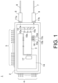
- the optical modulator 1 includes a housing 2 and an optical modulation element 3 accommodated in the housing 2 and generating an optical modulation signal by a traveling wave operation.
- the optical modulation element 3 has, for example, a nested Mach-Zehnder type coherent communication modulator configuration compatible with a polarization synthesis modulation method, and is compatible with multi-level modulation formats such as DP-QPSK and QAM modulation.
- the housing 2 complies with, for example, the HB-CDM standard (" Implementation Agreement for the High Bandwidth Coherent Driver Modulator (HB-CDM) OIF-HB-CDM-02.0" (published by OIF on July 15, 2021 )) which is the industry standard.
- a cover (not shown), which is a plate, is finally fixed to an opening of the housing 2, and the inside of the housing 2 is hermetically sealed.
- the input optical fiber 6 and the output optical fiber 7 are respectively fixed to the housing 2 via a support 8 and a support 9, which are fixing members.
- the light input from the input optical fiber 6 is collimated by a lens 11a arranged inside the support 8, and then passes through the beam shifter 12 to be input to the optical modulation element 3 via a lens 10a.
- this is merely an example, and the light may be input to the optical modulation element 3 by, for example, introducing the input optical fiber 6 into the housing 2 via the support 8 and connecting an end surface of the introduced input optical fiber 6 to an end surface of an optical substrate 30 (which will be described later) of the optical modulation element 3, according to the conventional technique.
- the drive circuit 17 may be mounted on the relay substrate 14 as shown in FIG. 1 , or may be disposed between the relay substrate 14 and the optical modulation element 3.
- the interface used for inputting the high frequency electrical signal may be an FPC (flexible printed circuit board) arranged outside the housing 2, instead of the signal pin 4.
- the optical substrate 30 is, for example, rectangular, and has two sides 32a and 32b on the left and right of the drawing that extend in the up-down direction of the drawing and face each other, and two sides 32c and 32d on the top and bottom of the drawing that extend in the left-right direction of the drawing and face each other.
- the nested Mach-Zehnder type optical waveguides 35a and 35b turn the propagation direction of the light by 180 degrees at a folding region 38 in the left part of the drawing on the optical substrate 30, and output the light from the side 32b of the optical substrate 30 to the right of the drawing by output waveguides 36a and 36b.
- a bias electrode part 40 in the upper part of the drawing of the nested Mach-Zehnder type optical waveguides 35a and 35b, which are folded back at the folding region 38 in the left part of the drawing on the optical substrate 30, is provided with, for example, bias electrodes 19 for adjusting the operating point of each of the four Mach-Zehnder type optical waveguides 37a, 37b, 37c, and 37d of the nested Mach-Zehnder type optical waveguides 35a and 35b, according to the conventional technique.
- bias electrodes 51 are formed on the optical substrate 30 to adjust the operating points of the nested Mach-Zehnder type optical waveguides 35a and 35b.
- four drive signals output from the drive circuit 17 are respectively input to the corresponding center electrodes 18 from the left side of FIG. 2 , become traveling waves and propagate through the center electrodes 18 toward the right side of the drawing, and are terminated by the corresponding terminal resistors 15 after the light waves propagating through the corresponding Mach-Zehnder type optical waveguides 37 are modulated in the RF electrode part 41.
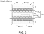
- FIG. 3 is a partial detailed view of part A in FIG. 2 , and is a view showing the electrode configuration of the Mach-Zehnder type optical waveguide 37c in the RF electrode part 41.
- the other Mach-Zehnder type optical waveguides 37a, 37b, and 37d in the RF electrode part 41 have similar electrode configurations to the Mach-Zehnder type optical waveguide 37c shown in FIG. 3 .
- light enters from the left side of the drawing and exits from the right side of the drawing.
- the optical modulation element 3 which is an optical waveguide element, includes a control electrode 42 in the RF electrode part 41 to control the light waves propagating through the Mach-Zehnder type optical waveguide 37c.
- the control electrode 42 includes one first control electrode 43 and two second control electrodes 44.
- the first control electrode 43 is a part of the center electrode 18 described above, and actually extends from left to right in the drawing to be connected to other portions of the center electrode 18.
- the two second control electrodes are ground electrodes that respectively sandwich the center electrode 18 from a certain distance apart, and are connected to a ground potential via the conductive pattern (not shown) that extends on the main surface of the optical substrate 30, according to the conventional technique.
- the first control electrode 43 which is a part of the center electrode 18, is arranged between the parallel waveguides 39a and 39b of the Mach-Zehnder type optical waveguide 37c, which is a part of the optical waveguide 31.
- the two second control electrodes 44 which are ground electrodes, are arranged at positions facing the first control electrode 43 across the parallel waveguides 39a and 39b.
- the first control electrode 43 and the second control electrodes 44 are made of, for example, gold (Au), and chromium (Cr) may be used as the base metal to improve adhesion to the optical substrate 30.
- parallel waveguides 39a and 39b will also be collectively referred to as parallel waveguides 39.
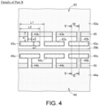
- FIG. 4 is a partial detailed view of part B of the RF electrode part 41 shown in FIG. 3 .
- FIG. 5 and FIG. 6 are cross-sectional views taken along line V-V and line VI-VI of part B shown in FIG. 4 .
- Part B shown in FIG. 4 illustrates one of the second control electrodes 44 and the first control electrode 43 that face each other across one parallel waveguide 39b of the Mach-Zehnder type optical waveguide 37c.
- the other second control electrode 44 and the first control electrode 43 that face each other across the other parallel waveguide 39a in FIG. 2 are configured similarly to the configuration shown in FIG. 4 .
- the first control electrode 43 includes a common electrode 43a and a plurality of segment electrodes 43c.
- the common electrode 43a extends along the parallel waveguide 39b and propagates a high frequency signal.
- the segment electrodes 43c are divided along the extending direction of the parallel waveguide 39b and arranged closer to the parallel waveguide 39b than the common electrode 43a.
- the first control electrode 43 further includes a plurality of connection electrodes 43b that respectively connect the plurality of segment electrodes 43c to the common electrode 43a.
- the second control electrode 44 includes a common electrode 44a and a plurality of segment electrodes 44c.
- the common electrode 44a extends along the parallel waveguide 39b and propagates a high frequency signal.
- the segment electrodes 44c are divided along the extending direction of the parallel waveguide 39b and arranged closer to the parallel waveguide 39b than the common electrode 44a.
- the second control electrode 44 further includes a plurality of connection electrodes 44b that respectively connect the plurality of segment electrodes 44c to the common electrode 44a.
- a low dielectric layer 45 that has a lower relative dielectric constant than the optical substrate is arranged between the lower portions of the common electrodes 43a and 44a and the optical substrate 30.
- the relative dielectric constant of the low dielectric layer 45 is preferably 1 or more and 10 or less.
- the low dielectric layer 45 may extend to a part of the connection electrodes 43b and 44b, as shown in FIG. 4 and FIG. 6 .
- the low dielectric layer 45 may be made of, for example, SiO 2 , low dielectric resin such as BCB (benzocyclobutene), silicon nitride, or the like.
- an optical modulation operation is performed by applying an electric field to the parallel waveguide 39 using the segment electrodes 43c and 44c provided close to the parallel waveguide 39, which may achieve low voltage driving. Furthermore, since the optical modulation element 3 has the low dielectric layer 45 between the common electrodes 43a and 44a through which the high frequency signal propagates and the optical substrate 30, the propagation speed of the high frequency signal in the common electrodes 43a and 44a (hereinafter also referred to as signal propagation speed) may be increased to improve the consistency (degree of coincidence) between the propagation speed of light waves propagating through the parallel waveguide 39b (hereinafter also referred to as waveguide speed) and the signal propagation speed. Thereby, the optical modulation element 3 is capable of achieving low voltage driving at a high modulation speed.
- the low dielectric layer 45 is configured to extend to the middle of the connection electrodes 43b and 44b in the example shown in FIG. 3 , FIG. 4 , FIG. 5 , and FIG. 6 , the low dielectric layer 45 may be configured to extend to the entire connection electrodes 43b and 44b.
- the low dielectric layer 45 is preferably configured with a thickness of 0.1 ⁇ m or more and 20 ⁇ m or less, which is appropriate for light speed matching.
- preferred sizes of the first control electrode 43 and the second control electrode 44 are as follows.
- the length a (see FIG. 4 ) of the connection electrodes 43b and 44b from the common electrodes 43a and 44a to the segment electrodes 43c and 44c, respectively, is 1 ⁇ m or more and 50 ⁇ m or less.
- the width W2 of the connection electrodes 43b and 44b measured in the extending direction of the parallel waveguide 39b is 1 ⁇ m or more and 10 ⁇ m or less.
- the width W1 of the segment electrodes 43c and 44c measured in the direction perpendicular to the extending direction of the parallel waveguide 39b is 1 ⁇ m or more and 10 ⁇ m or less.
- the pitch L1 between the segment electrodes 43c and between the segment electrodes 44c measured in the extending direction of the parallel waveguide 39b is 20 ⁇ m or more and 500 ⁇ m or less.
- the length L2 of the segment electrodes 43c and 44c measured in the extending direction of the parallel waveguide 39b is L 1/2 or more and (L1-1 ⁇ m) or less.
- the other main surface of the optical substrate 30, opposite to the main surface on which the optical waveguide 31 is arranged is joined to a low dielectric substrate 46 so as to be in contact with the low dielectric substrate 46 (see FIG. 5 and FIG. 6 ).
- the low dielectric substrate 46 is made of a material having a lower relative dielectric constant than the optical substrate, preferably, a low dielectric material having a relative dielectric constant of 1 or more and 10 or less. Thereby, it is easier to increase the propagation speed of the high frequency signal in the control electrode 42, and the degree of freedom in designing the control electrode 42 is improved.
- the low dielectric material constituting the low dielectric substrate 46 preferably has a coefficient of linear expansion of 0.5 ⁇ 10 -6 or more and 10 ⁇ 10 -6 or less from the viewpoint of reducing stress at the boundary between the optical substrate 30 and the low dielectric substrate 46 that may occur due to fluctuations in operating temperature.
- a low dielectric material may be, for example, SiO 2 .
- the thickness of the low dielectric substrate 46 is preferably 0.1 ⁇ m or more and 1000 ⁇ m or less, for example.
- a holding substrate (not shown) may be attached to the back surface of the low dielectric substrate 46 (that is, the surface opposite to the surface to be joined to the optical substrate 30) to reinforce the mechanical strength of the optical modulation element 3.
- a holding substrate may be made of, for example, Si or glass.
- optical modulation element 3 which is an optical waveguide element
- the low dielectric layer 45 may extend below the connection electrodes 43b and 44b and the segment electrodes 43c and 44c.
- FIG. 7 and FIG. 8 are views showing the configuration of the control electrode 42 of the optical modulation element 3 according to such a first modified example.
- FIG. 7 and FIG. 8 are views corresponding to the V-V cross-sectional view shown in FIG. 5 and the VI-VI cross-sectional view shown in FIG. 6 , respectively.
- the low dielectric layer 45 extends from below the common electrodes 43a and 44a to below the segment electrodes 43c and 44c, respectively.
- the portions of the first control electrode 43 and the second control electrode 44 sandwiching the parallel waveguide 39a are also configured similarly to the configuration shown in FIG. 7 and FIG. 8 .
- optical modulation element 3 it is easy to increase the propagation speed of microwaves (electrical signal) and match the speeds of light and electrical signal throughout the entire first control electrode and the entire second control electrode 44 including the segment electrodes 44c.
- the low dielectric layer 45 extends from below the common electrodes 43a and 44a to the middle below the segment electrodes 43c and 44c, respectively, in the example of FIG. 7 and FIG. 8 , the low dielectric layer 45 may extend to the entirety below the segment electrodes 43c and 44c.
- each of the segment electrodes 43c and 44c is configured so that at least the lower portion of the surface adjacent to the parallel waveguide 39b is formed on the optical substrate 30 without the low dielectric layer 45 therebetween, thereby increasing the strength of the electric field that the segment electrodes 43c and 44c give to the parallel waveguide 39b, improving the electric field efficiency in the optical modulation operation (that is, the ratio of the electric field used for the optical modulation operation to the electric field generated by the control electrode 42), and reducing the driving voltage required for operating the optical modulation element 3.
- metal materials such as nickel and titanium that are used as the electrode base film when forming electrodes of gold or the like have higher adhesion to the surface of the optical substrate 30 made of LN or the like, which has an elastic modulus equal to or higher than the elastic modulus of these metal materials and is highly hydrophilic, compared to adhesion to the surface of the low dielectric layer 45 made of resin or the like. Therefore, with the configuration as described above, the portions of the segment electrodes 43c and 44c formed on the optical substrate 30 without the low dielectric layer 45 therebetween have improved adhesion to the optical substrate 30, which may, as a result, improve the reliability of the optical modulation element 3.
- the low dielectric layer 45 in the cross section perpendicular to the extending direction of the parallel waveguide 39, preferably has a curved corner between the side adjacent to the optical waveguide and the upper side that is a side far from the substrate.
- FIG. 9 and FIG. 10 are views showing the configuration of the control electrode 42 of the optical modulation element 3 according to such a second modified example.
- FIG. 9 and FIG. 10 are views corresponding to the V-V cross-sectional view shown in FIG. 5 and the VI-VI cross-sectional view shown in FIG. 6 , respectively.
- the low dielectric layer 45 extending below the common electrodes 43a and 44a each has an R part 49 that is curved (portion within the circle indicated by the dashed line shown in FIG. 9 and FIG.
- the portions of the first control electrode 43 and the second control electrode 44 sandwiching the parallel waveguide 39a are also configured similarly to the configuration shown in FIG. 9 and FIG. 10 .
- the thickness of the conductor of the control electrode 42 at the transition portion from the conductor portion formed on top of the low dielectric layer 45 to the conductor portion formed on the optical substrate 30 without the low dielectric layer 45 therebetween changes continuously, which may reduce loss (for example, radiation loss) of the high frequency signal that propagates through the transition portion.
- loss for example, radiation loss
- stress on the connection electrodes 43b and 44b that may occur at the corner may be reduced to further improve the reliability of the optical modulation element 3, compared to a case where the corner has a bent shape.
- a buffer layer may be provided between the segment electrodes 43c and 44c and the optical substrate 30.
- FIG. 11 and FIG. 12 are views showing the configuration of the control electrode 42 of the optical modulation element 3 according to such a third modified example.
- FIG. 11 and FIG. 12 are views corresponding to the V-V cross-sectional view shown in FIG. 5 and the VI-VI cross-sectional view shown in FIG. 6 , respectively.
- a buffer layer 47 is arranged to cover the parallel waveguide 39b and extend below the segment electrodes 43c and 44c.
- the buffer layer 47 may also be arranged for the portions of the first control electrode 43 and the second control electrode 44 sandwiching the parallel waveguide 39a in the same manner as in the configuration shown in FIG. 11 and FIG. 12 .
- the buffer layer 47 extends along the length direction of the parallel waveguide 39 (the normal direction to the plane of the paper of FIG. 11 and FIG. 12 ).
- the metal (for example, Au, Cr or the like) constituting the segment electrodes 43c and 44c arranged close to the parallel waveguide 39 may prevent loss of light waves propagating through the parallel waveguide 39 (so-called light absorption loss).
- the amount of off-light in the on/off operation of output light in the optical modulation element 3 is determined by stray light propagating within the optical substrate 30, and does not depend much on the above-mentioned light absorption loss.
- the amount of on-light in the on/off operation depends on the light absorption loss and the magnitude of the driving voltage. Therefore, when the light absorption loss is large, the amount of on-light decreases even with the same driving voltage, and the extinction ratio of the modulated light output from the optical modulation element 3 deteriorates.
- the light absorption loss may be reduced to ensure a high extinction ratio, so the driving voltage required to obtain a predetermined extinction ratio may be reduced.
- the buffer layer 47 is not formed below the low dielectric layer 45 in the example shown in FIG. 10 and FIG. 11 , the buffer layer 47 may be formed over the entire optical substrate 30 including the bottom of the low dielectric layer 45.
- the low dielectric layer 45 has one or more through holes extending in the thickness direction of the low dielectric layer 45, and the control electrode 42 is configured to extend through the through hole to reach the main surface of the optical substrate.
- FIG. 13 and FIG. 14 are views showing the configuration of the control electrode 42 of the optical modulation element 3 according to such a fourth modified example.
- FIG. 13 is a view corresponding to FIG. 3 showing the configuration of the RF electrode part 41 in the Mach-Zehnder type optical waveguide 37c.
- FIG. 14 is a cross-sectional view taken along line XIV-XIV in FIG. 13 .
- a plurality of through holes 48 (circles indicated by dotted lines in the drawing), which are circular in plan view, are arranged in a matrix in the low dielectric layer 45 arranged below the first control electrode 43 and the second control electrode 44. Then, as shown in FIG.
- the common electrode 44a of the second control electrode 44 extends to the main surface of the optical substrate 30 through the through holes 48 (rectangles indicated by dotted lines in the drawing).
- the through holes 48 (rectangles indicated by dotted lines in the drawing).
- FIG. 13 only one through hole 48 is labeled with a reference numeral as an example, all the circles indicated by dotted lines in the drawing represent the through holes 48.
- control electrode 42 passes through the through holes 48 and directly comes into close contact with the optical substrate 30. Therefore, similar to the configuration of FIG. 7 and FIG. 8 described above, for example, even when the low dielectric layer 45 is made of resin, the adhesion between the control electrode 42 and the optical substrate 30 may be increased to improve the reliability of the optical modulation element 3.
- the diameter r (see FIG. 13 ) of the through hole 48 is preferably 1 ⁇ m or more and 25 ⁇ m or less, for example.
- the arrangement intervals d1 and d2 between the through holes 48 in the extending direction of the parallel waveguide 39 and the direction perpendicular thereto are preferably 50 ⁇ m or more and 500 ⁇ m or less.
- the through hole 48 is not limited to a circular shape, and may have any shape in plan view. In this case, it is desirable to configure the through hole 48 so that the opening area thereof on the side of the optical substrate 30 is approximately the same as the opening area of the circular through hole having a diameter of 1 ⁇ m or more and 25 ⁇ m or less in plan view. Furthermore, the through holes 48 are not necessarily arranged in a matrix, and may be arranged in any regular pattern or irregular pattern. Even in this case, the arrangement interval between the through holes 48 is preferably 50 ⁇ m or more and 500 ⁇ m or less.
- the through holes 48 shown in the fourth modified example described above may be formed only for the second control electrode 44 and not for the first control electrode 43.
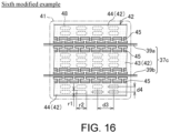
- the through hole 48 shown in the fourth modified example described above may not be circular in plan view, and may be an ellipse that extends in the extending direction of the parallel waveguides 39a and 39b.
- This configuration is capable of increasing the area of the through hole 48 to improve the adhesion between the control electrode 42 and the optical substrate 30, and preventing the propagation of the high frequency signal in the control electrode 42 from being inhibited by the through hole 48.
- the length r2 of the elliptical through hole 48 is at least twice the width r1 and at most 10 times the width r1. Further, regarding the arrangement interval between adjacent through holes 48, preferably the arrangement interval d2 in the length direction of the through holes 48 is at least twice the arrangement interval d1 in the width direction and at most 10 times.
- each portion of the optical waveguide 31, which is a convex optical waveguide may be formed by a band-shaped convex portion sandwiched between two grooves extending at a predetermined separation distance from each other on the main surface of the optical substrate 30.
- FIG. 17 , FIG. 18 , FIG. 19 , and FIG. 20 are views showing the configuration of the Mach-Zehnder type optical waveguide 37c of the optical modulation element 3 according to such a seventh modified example, and are views corresponding to FIG. 3 , FIG. 4 , FIG. 5 , and FIG. 6 .
- FIG. 18 is a partial detailed view of part C in FIG. 17 .
- FIG. 19 and FIG. 20 are a cross-sectional view taken along line XVII-XVII and a cross-sectional view taken along line XVIII-XVIII in FIG. 18 .
- each portion of the optical waveguide 31 is formed by a band-shaped convex portion sandwiched between any two of grooves 50a, 50b, and 50c extending at a predetermined separation distance on the main surface of the optical substrate 30.
- the parallel waveguide 39a is formed by a convex portion sandwiched between two grooves 50a and 50b
- the parallel waveguide 39b is formed by a convex portion sandwiched between two grooves 50a and 50c.
- FIG. 18 , FIG. 19 , and FIG. 20 are a plan view and cross-sectional views of the vicinity of the parallel waveguide 39b, and as described above, the parallel waveguide 39b is formed by a convex portion sandwiched between two grooves 50a and 50c.
- the optical waveguide 31, which is a convex waveguide, may be easily formed on the main surface of the optical substrate 30.
- segment electrodes 43c and 44c may be formed on the bottom surfaces of the grooves 50a and 50c, respectively, as shown in FIG. 19 and FIG. 20 .
- This embodiment is an optical transmission device 60 equipped with the optical modulator 1 according to the first embodiment or the modified examples thereof.
- FIG. 21 is a diagram showing the configuration of the optical transmission device 60 according to this embodiment.
- This optical transmission device 60 includes the optical modulator 1, a light source 61, and a modulation signal generator 62.
- the modulation signal generator 62 is an electronic circuit configured to generate a high frequency signal (modulation signal) for causing the optical modulator 1 to perform a modulation operation.
- the modulation signal generator 62 generates four modulation signals to be input to the optical modulation element 3 included in the optical modulator 1, based on transmission data given from the outside, and inputs the modulation signals to the signal pin 4 of the optical modulator 1.
- the optical modulator 1 modulates the light from the light source 61 that is incident from the input optical fiber 6, and outputs the modulated light through the output optical fiber 7.
- the various modified examples of the first embodiment described above may be arbitrarily combined to form one optical waveguide element (for example, the optical modulation element 3).
- the R part 49 of the low dielectric layer 45 in the second modified example (see FIG. 9 , etc.) and/or the through holes 48 of the low dielectric layer 45 in the fourth modified example may be applied in combination in all the other modified examples.
- the optical waveguide element in the disclosure is not limited to the optical modulation element 3 that performs an optical modulation operation using a nested Mach-Zehnder type optical waveguide, and may be various types of optical waveguide elements that achieve any function using optical waveguides formed in arbitrary patterns.
- the optical waveguide element may include not only a Mach-Zehnder type optical waveguide but also a directional coupler type waveguide and/or a Y-branch waveguide, and achieve a function such as optical switching.
- An optical waveguide element includes an optical waveguide arranged on a main surface of an optical substrate; and a control electrode configured to control light waves propagating through the optical waveguide.
- the control electrode includes a first control electrode and a second control electrode facing each other across the optical waveguide on the main surface of the optical substrate.
- Each of the first control electrode and the second control electrode includes a common electrode extending along the optical waveguide, a plurality of segment electrodes arranged closer to the optical waveguide than the common electrode and divided along an extending direction of the optical waveguide, and a plurality of connection electrodes connecting each of the plurality of segment electrodes to the common electrode.
- a low dielectric layer having a relative dielectric constant lower than a relative dielectric constant of the optical substrate is arranged between the common electrode and the optical substrate.
- the optical waveguide element of Configuration 1 is capable of applying an electric field to the optical waveguide using the segment electrodes arranged close to the optical waveguide while increasing the propagation speed of the high frequency signal in the common electrode, and therefore is capable of achieving low voltage driving at a high operating speed.
- the optical waveguide element of Configuration 2 is capable of reducing the waveguide loss of the high frequency signal in the control electrode and reducing the power required for the optical modulation operation.
- the optical waveguide includes a Mach-Zehnder type optical waveguide that includes two parallel waveguides.
- the control electrode includes one first control electrode arranged between the two parallel waveguides; and two second control electrodes facing the first control electrode respectively across the two parallel waveguides.
- the optical waveguide element of Configuration 3 is capable of achieving low voltage driving at a high operating speed in an optical waveguide including a Mach-Zehnder type optical waveguide.
- the optical waveguide element of Configuration 4 is capable of disposing a portion of the segment electrode adjacent to the optical waveguide on the optical substrate and close to the optical waveguide while disposing the low dielectric layer below the segment electrode. Therefore, the optical waveguide element of Configuration 3 is capable of reducing the driving voltage while increasing the adhesion between the segment electrode and the optical substrate and improving reliability.
- the low dielectric layer includes a curved corner between a side adjacent to the optical waveguide and an upper side that is a side far from the optical substrate, in a cross section perpendicular to the extending direction of the optical waveguide.
- the corner of the low dielectric layer is curved, so the conductor thickness of the control electrode at the transition portion from the conductor portion formed on the low dielectric layer to the conductor portion formed directly on the optical substrate changes continuously through the curve. Therefore, compared to a case where the corner has a bent shape, the optical modulation element of Configuration 4 is capable of reducing loss (for example, radiation loss) of the high frequency signal that propagates through the transition portion, and is capable of reducing stress that may occur in the control electrode formed on top of the corner to further improve the reliability of the optical waveguide element.
- loss for example, radiation loss
- the propagation speed of the high frequency signal in the control electrode is easily increased, and the degree of freedom in designing the control electrode is improved.
- the optical waveguide element according to any one of Configurations 1 to 6 further includes a buffer layer between the segment electrodes and the optical substrate.
- the optical waveguide element of Configuration 7 is capable of preventing light absorption loss of light waves propagating through the optical waveguide with the metal constituting the segment electrodes arranged close to the optical waveguide.
- the low dielectric layer has one or more through holes extending in a thickness direction of the low dielectric layer, and the control electrode extends through the one or more through holes to the optical substrate.
- the control electrode has a portion that passes through the through hole and comes into direct contact with the optical substrate.
- the adhesion between the control electrode and the optical substrate may be increased to improve the reliability of the optical waveguide element.
- An optical modulator includes the optical waveguide element according to any one of Configurations 1 to 8, which is an optical modulation element; a housing configured to accommodate the optical waveguide element; an optical fiber configured to input light to the optical waveguide element; and an optical fiber configured to guide light output by the optical waveguide element to outside of the housing.
- the optical modulator of Configuration 9 is capable of achieving an optical modulation operation that enables low voltage driving at a high modulation speed.
- An optical transmission device includes the optical modulator according to Configuration 9; and an electronic circuit configured to generate an electrical signal for causing the optical waveguide element to perform an optical modulation operation.
- Mach-Zehnder type optical waveguide 38... folding region; 39a, 39b... parallel waveguide; 40, 40a, 40b... bias electrode part; 41... RF electrode part; 42... control electrode; 43... first control electrode; 44... second control electrode; 43a, 44a... common electrode; 43b, 44b... connection electrode; 43c, 44c... segment electrode; 45... low dielectric layer; 46... low dielectric substrate; 47... buffer layer; 48... through hole; 49... R part; 50a, 50b, 50c... groove; 60... optical transmission device; 61... light source; 62... modulation signal generator.
Landscapes
- Physics & Mathematics (AREA)
- Nonlinear Science (AREA)
- General Physics & Mathematics (AREA)
- Optics & Photonics (AREA)
- Chemical & Material Sciences (AREA)
- Engineering & Computer Science (AREA)
- Ceramic Engineering (AREA)
- Crystallography & Structural Chemistry (AREA)
- Electromagnetism (AREA)
- Optical Modulation, Optical Deflection, Nonlinear Optics, Optical Demodulation, Optical Logic Elements (AREA)
Abstract
Description
- The disclosure relates to an optical waveguide element, an optical modulator, and an optical transmission device.
- Optical modulators incorporating an optical modulation element as an optical waveguide element, which includes an optical waveguide formed on a substrate and a control electrode for controlling light waves propagating through the optical waveguide, are often used in high-speed/high-capacity optical fiber communication systems. Semiconductor optical modulation elements using semiconductor substrates, such as InP substrates, and LiNbO3 (hereinafter also referred to as LN) optical modulation elements using LN as the substrates have been practically used as optical waveguide elements for performing an optical modulation operation.
- In recent years, optical modulators for optical communication have been required to have a symbol rate of 100 GBaud or more as the modulation speed. Therefore, from the viewpoint of widening the frequency characteristics of optical modulation elements, electrical-optical speed matching (that is, matching between the speed of light propagating through the optical waveguide and the propagation speed of the high frequency signal propagating through the control electrode) and impedance matching (that is, matching between the impedance of the control electrode and the output impedance of the drive circuit that outputs the high frequency signal to the control electrode) are important.
- Conventionally, a control electrode having a capacity loaded type traveling wave electrode structure with a high degree of freedom in impedance adjustment has been proposed as a means for achieving the impedance matching (see, for example, Patent Document 1). In this control electrode, an RF electrode for propagating a high frequency signal is arranged on a dielectric layer formed on a substrate, and a plurality of segment electrodes divided in the extending direction of the optical waveguide are arranged on the substrate. Each segment electrode is connected to the RF electrode by a conductor that penetrates the dielectric layer to apply a high frequency electric field to the optical waveguide. Thus, in the conventional control electrode described above, the propagation speed of the high frequency signal in the RF electrode portion is increased to achieve optical-electrical speed matching.
- However, there have been demands for smaller size, wider bandwidth, and lower driving voltage, and for the conventional control electrode described above, when the distance between the RF electrode on the dielectric layer and the ground electrode is reduced in order to shorten the distance between segment electrodes that sandwich the optical waveguide on the substrate, the propagation speed of the high frequency signal in the RF electrode may drop. As a result, optical-electrical speed matching may become difficult, making it difficult to achieve low voltage driving at a high modulation speed.
- [Patent Document 1]
Japanese Patent Application Laid-Open No. 2016-194544 - In view of the above background, an object of the disclosure is to achieve low voltage driving at a high operating speed in an optical waveguide element.
- One aspect of the disclosure is an optical waveguide element that includes an optical waveguide arranged on a main surface of an optical substrate; and a control electrode configured to control light waves propagating through the optical waveguide. The control electrode includes a first control electrode and a second control electrode facing each other across the optical waveguide on the main surface of the optical substrate. Each of the first control electrode and the second control electrode includes a common electrode extending along the optical waveguide, a plurality of segment electrodes arranged closer to the optical waveguide than the common electrode and divided along an extending direction of the optical waveguide, and a plurality of connection electrodes connecting each of the plurality of segment electrodes to the common electrode. A low dielectric layer having a relative dielectric constant lower than a relative dielectric constant of the optical substrate is arranged between the common electrode and the optical substrate.
- According to another aspect of the disclosure, the low dielectric layer extends to below the connection electrodes and the segment electrodes.
- According to another aspect of the disclosure, the optical waveguide includes a Mach-Zehnder type optical waveguide that includes two parallel waveguides. The control electrode includes one first control electrode arranged between the two parallel waveguides; and two second control electrodes facing the first control electrode respectively across the two parallel waveguides.
- According to another aspect of the disclosure, at least a lower portion of a surface, adjacent to the optical waveguide, of the segment electrode is formed on the optical substrate without the low dielectric layer therebetween.
- According to another aspect of the disclosure, the low dielectric layer includes a curved corner between a side adjacent to the optical waveguide and an upper side that is a side far from the optical substrate, in a cross section perpendicular to the extending direction of the optical waveguide.
- According to another aspect of the disclosure, an other main surface of the optical substrate, opposite to the main surface on which the optical waveguide is arranged, is in contact with a low dielectric substrate composed of a low dielectric material with a relative dielectric constant of 1 or more and 10 or less.
- According to another aspect of the disclosure, a buffer layer is provided between the segment electrodes and the optical substrate.
- According to another aspect of the disclosure, the low dielectric layer has one or more through holes extending in a thickness direction of the low dielectric layer, and the control electrode extends through the one or more through holes to the optical substrate.
- Another aspect of the disclosure is an optical modulator that includes any of the above optical waveguide element which is an optical modulation element; a housing configured to accommodate the optical waveguide element; an optical fiber configured to input light to the optical waveguide element; and an optical fiber configured to guide light output by the optical waveguide element to outside of the housing.
- Another aspect of the disclosure is an optical transmission device that includes any of the above optical modulator; and an electronic circuit configured to generate an electrical signal for causing the optical waveguide element to perform an optical modulation operation.
- The disclosure is capable of achieving low voltage driving at a high operating speed in an optical waveguide element.
-
-
FIG. 1 is a diagram showing the configuration of the optical modulator according to the first embodiment of the disclosure. -
FIG. 2 is a diagram showing the configuration of the optical modulation element used in the optical modulator shown inFIG. 1 . -
FIG. 3 is a partial detailed view of part A of the RF electrode part shown inFIG. 2 . -
FIG. 4 is a partial detailed view of part B of the RF electrode part shown inFIG. 3 . -
FIG. 5 is a cross-sectional view taken along line V-V of part B shown inFIG. 4 . -
FIG. 6 is a cross-sectional view taken along line VI-VI of part B shown inFIG. 4 . -
FIG. 7 is a view showing the configuration of the optical modulation element according to the first modified example. -
FIG. 8 is a view showing the configuration of the optical modulation element according to the first modified example. -
FIG. 9 is a view showing the configuration of the optical modulation element according to the second modified example. -
FIG. 10 is a view showing the configuration of the optical modulation element according to the second modified example. -
FIG. 11 is a view showing the configuration of the optical modulation element according to the third modified example. -
FIG. 12 is a view showing the configuration of the optical modulation element according to the third modified example. -
FIG. 13 is a view showing the configuration of the optical modulation element according to the fourth modified example. -
FIG. 14 is a view showing the configuration of the optical modulation element according to the fourth modified example. -
FIG. 15 is a view showing the configuration of the optical modulation element according to the fifth modified example. -
FIG. 16 is a view showing the configuration of the optical modulation element according to the sixth modified example. -
FIG. 17 is a view showing the configuration of the optical modulation element according to the seventh modified example. -
FIG. 18 is a partial detailed view of part C shown inFIG. 17 . -
FIG. 19 is a cross-sectional view taken along line XVII-XVII of part C shown inFIG. 18 . -
FIG. 20 is a cross-sectional view taken along line XVIII-XVIII of part C shown inFIG. 18 . -
FIG. 21 is a diagram showing the configuration of the optical transmission device according to the second embodiment of the disclosure. - Embodiments of the disclosure will be described hereinafter with reference to the drawings.
- First, the first embodiment of the disclosure will be described.
FIG. 1 is a diagram showing the configuration of anoptical modulator 1 using an optical modulation element, which is an optical waveguide element, according to the first embodiment of the disclosure. - The
optical modulator 1 includes ahousing 2 and anoptical modulation element 3 accommodated in thehousing 2 and generating an optical modulation signal by a traveling wave operation. Theoptical modulation element 3 has, for example, a nested Mach-Zehnder type coherent communication modulator configuration compatible with a polarization synthesis modulation method, and is compatible with multi-level modulation formats such as DP-QPSK and QAM modulation. Thehousing 2 complies with, for example, the HB-CDM standard ("Implementation Agreement for the High Bandwidth Coherent Driver Modulator (HB-CDM) OIF-HB-CDM-02.0" (published by OIF on July 15, 2021)) which is the industry standard. A cover (not shown), which is a plate, is finally fixed to an opening of thehousing 2, and the inside of thehousing 2 is hermetically sealed. - The
housing 2 is provided with a signal pin 4 for inputting a high frequency electrical signal that is used for modulating theoptical modulation element 3 to adrive circuit 17 mounted on arelay substrate 14, which will be described later. Thehousing 2 is also provided with asignal pin 5 that is for inputting an electrical signal used for adjusting an operating point of theoptical modulation element 3, inputting power supply for the operation of thedrive circuit 17, and inputting and outputting a control signal required for operating thedrive circuit 17. - The
optical modulator 1 further includes, on the same surface of thehousing 2, an inputoptical fiber 6 for inputting a light into thehousing 2 and an output optical fiber 7 for guiding the light modulated by theoptical modulation element 3 to the outside of thehousing 2. In addition, theoptical modulator 1 includes abeam shifter 12 that has both a beam shifting function and a polarization combining function. - The input
optical fiber 6 and the output optical fiber 7 are respectively fixed to thehousing 2 via asupport 8 and asupport 9, which are fixing members. The light input from the inputoptical fiber 6 is collimated by alens 11a arranged inside thesupport 8, and then passes through thebeam shifter 12 to be input to theoptical modulation element 3 via alens 10a. However, this is merely an example, and the light may be input to theoptical modulation element 3 by, for example, introducing the inputoptical fiber 6 into thehousing 2 via thesupport 8 and connecting an end surface of the introduced inputoptical fiber 6 to an end surface of an optical substrate 30 (which will be described later) of theoptical modulation element 3, according to the conventional technique. - Two modulated lights output from the
optical modulation element 3 are respectively collimated by alens 10b and alens 10c, and then combined into one beam by the polarization combining function of thebeam shifter 12. The combined beam is focused by alens 11b arranged inside thesupport 9 and coupled to the output optical fiber 7. - The
relay substrate 14 and aterminator 16, which includes fourterminal resistors housing 2 of theoptical modulator 1. Hereinafter, theterminal resistors optical modulation element 3 and the terminal resistors 15 of theterminator 16 are electrically connected by, for example, wire bonding or the like. - The
relay substrate 14 includes thedrive circuit 17. Thedrive circuit 17 amplifies the high frequency electrical signal input from the signal pin 4 and outputs a drive signal which is a high frequency electrical signal for causing theoptical modulation element 3 to perform a modulation operation. Further, therelay substrate 14 relays the electrical signal for operating point adjustment or the like, power supply, and control signal inputted from thesignal pin 5 to theoptical modulation element 3. The conductive pattern of therelay substrate 14 is respectively connected to a pad (not shown) that forms one end of the electrode of theoptical modulation element 3 by, for example, wire bonding or the like. Although therelay substrate 14 is illustrated as a single substrate inFIG. 1 , therelay substrate 14 may be divided into a plurality of substrates as required. Furthermore, thedrive circuit 17 may be mounted on therelay substrate 14 as shown inFIG. 1 , or may be disposed between therelay substrate 14 and theoptical modulation element 3. Besides, the interface used for inputting the high frequency electrical signal may be an FPC (flexible printed circuit board) arranged outside thehousing 2, instead of the signal pin 4. -
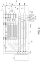
FIG. 2 is a diagram showing an example of the configuration of theoptical modulation element 3, which is a DP-QPSK modulator or the like. Theoptical modulation element 3 includes an optical waveguide 31 (the entirety thereof is indicated by thick dotted lines in the drawing) formed on one main surface (the surface shown inFIG. 2 ) of theoptical substrate 30 and performs coherent multi-level modulation exceeding 100 GBaud, for example. Theoptical substrate 30 is, for example, an X-cut LN substrate processed into a thin film having a thickness of 20 µm or less (for example, 2 µm) and having an electro-optic effect. In addition, theoptical waveguide 31 is a convex optical waveguide (for example, a rib-type optical waveguide or a ridgetype optical waveguide) formed on a surface of the thin-filmoptical substrate 30 and having a convex portion that extends in a band shape. - The
optical substrate 30 is, for example, rectangular, and has twosides sides - The
optical waveguide 31 includes an input waveguide 33 and abranch waveguide 34. The input waveguide 33 receives input light (the arrow pointing to the right of the drawing) from the inputoptical fiber 6 on the upper side of the drawing of theright side 32b of theoptical substrate 30. The branch waveguide 34 branches the input light into two lights that have the same amount of light. Theoptical waveguide 31 also includes so-called nested Mach-Zehnder typeoptical waveguides branch waveguide 34. - The nested Mach-Zehnder type
optical waveguides folding region 38 in the left part of the drawing on theoptical substrate 30, and output the light from theside 32b of theoptical substrate 30 to the right of the drawing byoutput waveguides - The nested Mach-Zehnder type
optical waveguides optical waveguides optical waveguides optical waveguides - A
bias electrode part 40 in the upper part of the drawing of the nested Mach-Zehnder typeoptical waveguides folding region 38 in the left part of the drawing on theoptical substrate 30, is provided with, for example,bias electrodes 19 for adjusting the operating point of each of the four Mach-Zehnder typeoptical waveguides optical waveguides bias electrodes 51 are formed on theoptical substrate 30 to adjust the operating points of the nested Mach-Zehnder typeoptical waveguides - Additionally, in an
RF electrode part 41 in the lower part of the drawing of the nested Mach-Zehnder typeoptical waveguides folding region 38, fourcenter electrodes 18 through which the high frequency electrical signal is propagated are respectively arranged between two parallel waveguides of the corresponding Mach-Zehnder type optical waveguide 37 so as to perform a modulation operation for each of the total four Mach-Zehnder typeoptical waveguides optical waveguides - In
FIG. 2 , each of thecenter electrodes 18 constitutes a distributed constant line having a predetermined impedance together with two ground electrodes (not shown) that are formed on the main surface of theoptical substrate 30 so as to sandwich thecenter electrode 18 from a certain distance apart, according to the conventional technique. - Thus, four drive signals output from the
drive circuit 17 are respectively input to thecorresponding center electrodes 18 from the left side ofFIG. 2 , become traveling waves and propagate through thecenter electrodes 18 toward the right side of the drawing, and are terminated by the corresponding terminal resistors 15 after the light waves propagating through the corresponding Mach-Zehnder type optical waveguides 37 are modulated in theRF electrode part 41. -
FIG. 3 is a partial detailed view of part A inFIG. 2 , and is a view showing the electrode configuration of the Mach-Zehnder typeoptical waveguide 37c in theRF electrode part 41. The other Mach-Zehnder typeoptical waveguides RF electrode part 41 have similar electrode configurations to the Mach-Zehnder typeoptical waveguide 37c shown inFIG. 3 . InFIG. 3 , light enters from the left side of the drawing and exits from the right side of the drawing. - The
optical modulation element 3, which is an optical waveguide element, includes acontrol electrode 42 in theRF electrode part 41 to control the light waves propagating through the Mach-Zehnder typeoptical waveguide 37c. Thecontrol electrode 42 includes onefirst control electrode 43 and twosecond control electrodes 44. Here, thefirst control electrode 43 is a part of thecenter electrode 18 described above, and actually extends from left to right in the drawing to be connected to other portions of thecenter electrode 18. Further, the two second control electrodes are ground electrodes that respectively sandwich thecenter electrode 18 from a certain distance apart, and are connected to a ground potential via the conductive pattern (not shown) that extends on the main surface of theoptical substrate 30, according to the conventional technique. - On the main surface of the
optical substrate 30, thefirst control electrode 43, which is a part of thecenter electrode 18, is arranged between theparallel waveguides optical waveguide 37c, which is a part of theoptical waveguide 31. The twosecond control electrodes 44, which are ground electrodes, are arranged at positions facing thefirst control electrode 43 across theparallel waveguides first control electrode 43 and thesecond control electrodes 44 are made of, for example, gold (Au), and chromium (Cr) may be used as the base metal to improve adhesion to theoptical substrate 30. - Hereinafter, the
parallel waveguides -
FIG. 4 is a partial detailed view of part B of theRF electrode part 41 shown inFIG. 3 .FIG. 5 andFIG. 6 are cross-sectional views taken along line V-V and line VI-VI of part B shown inFIG. 4 . - Part B shown in
FIG. 4 illustrates one of thesecond control electrodes 44 and thefirst control electrode 43 that face each other across oneparallel waveguide 39b of the Mach-Zehnder typeoptical waveguide 37c. The othersecond control electrode 44 and thefirst control electrode 43 that face each other across the otherparallel waveguide 39a inFIG. 2 are configured similarly to the configuration shown inFIG. 4 . - As shown in
FIG. 4 , thefirst control electrode 43 includes acommon electrode 43a and a plurality ofsegment electrodes 43c. Thecommon electrode 43a extends along theparallel waveguide 39b and propagates a high frequency signal. Thesegment electrodes 43c are divided along the extending direction of theparallel waveguide 39b and arranged closer to theparallel waveguide 39b than thecommon electrode 43a. Thefirst control electrode 43 further includes a plurality ofconnection electrodes 43b that respectively connect the plurality ofsegment electrodes 43c to thecommon electrode 43a. - Similarly, the
second control electrode 44 includes acommon electrode 44a and a plurality ofsegment electrodes 44c. Thecommon electrode 44a extends along theparallel waveguide 39b and propagates a high frequency signal. Thesegment electrodes 44c are divided along the extending direction of theparallel waveguide 39b and arranged closer to theparallel waveguide 39b than thecommon electrode 44a. Thesecond control electrode 44 further includes a plurality ofconnection electrodes 44b that respectively connect the plurality ofsegment electrodes 44c to thecommon electrode 44a. - Then, as shown in
FIG. 5 andFIG. 6 , alow dielectric layer 45 that has a lower relative dielectric constant than the optical substrate is arranged between the lower portions of thecommon electrodes optical substrate 30. The relative dielectric constant of thelow dielectric layer 45 is preferably 1 or more and 10 or less. Thelow dielectric layer 45 may extend to a part of theconnection electrodes FIG. 4 andFIG. 6 . Thelow dielectric layer 45 may be made of, for example, SiO2, low dielectric resin such as BCB (benzocyclobutene), silicon nitride, or the like. - In the
optical modulation element 3 having the above configuration, an optical modulation operation is performed by applying an electric field to the parallel waveguide 39 using thesegment electrodes optical modulation element 3 has thelow dielectric layer 45 between thecommon electrodes optical substrate 30, the propagation speed of the high frequency signal in thecommon electrodes parallel waveguide 39b (hereinafter also referred to as waveguide speed) and the signal propagation speed. Thereby, theoptical modulation element 3 is capable of achieving low voltage driving at a high modulation speed. - Although the
low dielectric layer 45 is configured to extend to the middle of theconnection electrodes FIG. 3 ,FIG. 4 ,FIG. 5 , andFIG. 6 , thelow dielectric layer 45 may be configured to extend to theentire connection electrodes - From the viewpoint of achieving high-speed modulation and low voltage driving, the
low dielectric layer 45 is preferably configured with a thickness of 0.1 µm or more and 20 µm or less, which is appropriate for light speed matching. - In addition, in this embodiment, preferred sizes of the
first control electrode 43 and thesecond control electrode 44 are as follows. The length a (seeFIG. 4 ) of theconnection electrodes common electrodes segment electrodes connection electrodes parallel waveguide 39b is 1 µm or more and 10 µm or less. Further, the width W1 of thesegment electrodes parallel waveguide 39b is 1 µm or more and 10 µm or less. - Furthermore, the pitch L1 between the
segment electrodes 43c and between thesegment electrodes 44c measured in the extending direction of theparallel waveguide 39b is 20 µm or more and 500 µm or less. Further, the length L2 of thesegment electrodes parallel waveguide 39b isL 1/2 or more and (L1-1 µm) or less. - In this embodiment, as a more preferable configuration, the other main surface of the
optical substrate 30, opposite to the main surface on which theoptical waveguide 31 is arranged, is joined to a lowdielectric substrate 46 so as to be in contact with the low dielectric substrate 46 (seeFIG. 5 andFIG. 6 ). The lowdielectric substrate 46 is made of a material having a lower relative dielectric constant than the optical substrate, preferably, a low dielectric material having a relative dielectric constant of 1 or more and 10 or less. Thereby, it is easier to increase the propagation speed of the high frequency signal in thecontrol electrode 42, and the degree of freedom in designing thecontrol electrode 42 is improved. The low dielectric material constituting the lowdielectric substrate 46 preferably has a coefficient of linear expansion of 0.5×10⁻⁶ or more and 10×10-6 or less from the viewpoint of reducing stress at the boundary between theoptical substrate 30 and the lowdielectric substrate 46 that may occur due to fluctuations in operating temperature. Such a low dielectric material may be, for example, SiO2. The thickness of the lowdielectric substrate 46 is preferably 0.1 µm or more and 1000 µm or less, for example. - In the case of using the low
dielectric substrate 46 having a thickness of 300 µm or less, a holding substrate (not shown) may be attached to the back surface of the low dielectric substrate 46 (that is, the surface opposite to the surface to be joined to the optical substrate 30) to reinforce the mechanical strength of theoptical modulation element 3. Such a holding substrate may be made of, for example, Si or glass. - Next, modified examples of the
optical modulation element 3, which is an optical waveguide element, will be described. - As the first modified example of the
optical modulation element 3, thelow dielectric layer 45 may extend below theconnection electrodes segment electrodes -
FIG. 7 andFIG. 8 are views showing the configuration of thecontrol electrode 42 of theoptical modulation element 3 according to such a first modified example. Here,FIG. 7 andFIG. 8 are views corresponding to the V-V cross-sectional view shown inFIG. 5 and the VI-VI cross-sectional view shown inFIG. 6 , respectively. In the example shown inFIG. 7 andFIG. 8 , thelow dielectric layer 45 extends from below thecommon electrodes segment electrodes first control electrode 43 and thesecond control electrode 44 sandwiching theparallel waveguide 39a are also configured similarly to the configuration shown inFIG. 7 andFIG. 8 . - Thus, with the
optical modulation element 3 according to the first modified example, it is easy to increase the propagation speed of microwaves (electrical signal) and match the speeds of light and electrical signal throughout the entire first control electrode and the entiresecond control electrode 44 including thesegment electrodes 44c. - Although the
low dielectric layer 45 extends from below thecommon electrodes segment electrodes FIG. 7 andFIG. 8 , thelow dielectric layer 45 may extend to the entirety below thesegment electrodes - However, as shown in
FIG. 7 andFIG. 8 , each of thesegment electrodes parallel waveguide 39b is formed on theoptical substrate 30 without thelow dielectric layer 45 therebetween, thereby increasing the strength of the electric field that thesegment electrodes parallel waveguide 39b, improving the electric field efficiency in the optical modulation operation (that is, the ratio of the electric field used for the optical modulation operation to the electric field generated by the control electrode 42), and reducing the driving voltage required for operating theoptical modulation element 3. - In general, metal materials such as nickel and titanium that are used as the electrode base film when forming electrodes of gold or the like have higher adhesion to the surface of the
optical substrate 30 made of LN or the like, which has an elastic modulus equal to or higher than the elastic modulus of these metal materials and is highly hydrophilic, compared to adhesion to the surface of thelow dielectric layer 45 made of resin or the like. Therefore, with the configuration as described above, the portions of thesegment electrodes optical substrate 30 without thelow dielectric layer 45 therebetween have improved adhesion to theoptical substrate 30, which may, as a result, improve the reliability of theoptical modulation element 3. - As the second modified example of the
optical modulation element 3, in the cross section perpendicular to the extending direction of the parallel waveguide 39, thelow dielectric layer 45 preferably has a curved corner between the side adjacent to the optical waveguide and the upper side that is a side far from the substrate. -
FIG. 9 andFIG. 10 are views showing the configuration of thecontrol electrode 42 of theoptical modulation element 3 according to such a second modified example. Here,FIG. 9 andFIG. 10 are views corresponding to the V-V cross-sectional view shown inFIG. 5 and the VI-VI cross-sectional view shown inFIG. 6 , respectively. As shown inFIG. 9 andFIG. 10 , thelow dielectric layer 45 extending below thecommon electrodes R part 49 that is curved (portion within the circle indicated by the dashed line shown inFIG. 9 andFIG. 10 ) at the corner between the side adjacent to theparallel waveguide 39b and the upper side that is the side far from theoptical substrate 30, in the cross section perpendicular to the extending direction of theparallel waveguide 39b (that is, in the cross section shown inFIG. 9 andFIG. 10 ). The portions of thefirst control electrode 43 and thesecond control electrode 44 sandwiching theparallel waveguide 39a are also configured similarly to the configuration shown inFIG. 9 andFIG. 10 . - Thus, in the
optical modulation element 3 according to the second modified example, the thickness of the conductor of thecontrol electrode 42 at the transition portion from the conductor portion formed on top of thelow dielectric layer 45 to the conductor portion formed on theoptical substrate 30 without thelow dielectric layer 45 therebetween changes continuously, which may reduce loss (for example, radiation loss) of the high frequency signal that propagates through the transition portion. Particularly, in the case where a corner having theR part 49 is provided at the lower part of theconnection electrodes connection electrodes optical modulation element 3, compared to a case where the corner has a bent shape. - As the third modified example of the
optical modulation element 3, a buffer layer may be provided between thesegment electrodes optical substrate 30. -
FIG. 11 andFIG. 12 are views showing the configuration of thecontrol electrode 42 of theoptical modulation element 3 according to such a third modified example. Here,FIG. 11 andFIG. 12 are views corresponding to the V-V cross-sectional view shown inFIG. 5 and the VI-VI cross-sectional view shown inFIG. 6 , respectively. In the illustrated example, abuffer layer 47 is arranged to cover theparallel waveguide 39b and extend below thesegment electrodes buffer layer 47 may also be arranged for the portions of thefirst control electrode 43 and thesecond control electrode 44 sandwiching theparallel waveguide 39a in the same manner as in the configuration shown inFIG. 11 andFIG. 12 . Thebuffer layer 47 extends along the length direction of the parallel waveguide 39 (the normal direction to the plane of the paper ofFIG. 11 andFIG. 12 ). - Thus, the metal (for example, Au, Cr or the like) constituting the
segment electrodes - Generally, the amount of off-light in the on/off operation of output light in the
optical modulation element 3 is determined by stray light propagating within theoptical substrate 30, and does not depend much on the above-mentioned light absorption loss. On the other hand, the amount of on-light in the on/off operation depends on the light absorption loss and the magnitude of the driving voltage. Therefore, when the light absorption loss is large, the amount of on-light decreases even with the same driving voltage, and the extinction ratio of the modulated light output from theoptical modulation element 3 deteriorates. - In contrast thereto, in the configuration that includes the buffer layer as described above, the light absorption loss may be reduced to ensure a high extinction ratio, so the driving voltage required to obtain a predetermined extinction ratio may be reduced.
- Although the
buffer layer 47 is not formed below thelow dielectric layer 45 in the example shown inFIG. 10 andFIG. 11 , thebuffer layer 47 may be formed over the entireoptical substrate 30 including the bottom of thelow dielectric layer 45. - As the fourth modified example of the
optical modulation element 3, thelow dielectric layer 45 has one or more through holes extending in the thickness direction of thelow dielectric layer 45, and thecontrol electrode 42 is configured to extend through the through hole to reach the main surface of the optical substrate. -
FIG. 13 andFIG. 14 are views showing the configuration of thecontrol electrode 42 of theoptical modulation element 3 according to such a fourth modified example. Here,FIG. 13 is a view corresponding toFIG. 3 showing the configuration of theRF electrode part 41 in the Mach-Zehnder typeoptical waveguide 37c. Further,FIG. 14 is a cross-sectional view taken along line XIV-XIV inFIG. 13 . In the example shown inFIG. 13 , a plurality of through holes 48 (circles indicated by dotted lines in the drawing), which are circular in plan view, are arranged in a matrix in thelow dielectric layer 45 arranged below thefirst control electrode 43 and thesecond control electrode 44. Then, as shown inFIG. 14 , for example, thecommon electrode 44a of thesecond control electrode 44 extends to the main surface of theoptical substrate 30 through the through holes 48 (rectangles indicated by dotted lines in the drawing). Although inFIG. 13 , only one throughhole 48 is labeled with a reference numeral as an example, all the circles indicated by dotted lines in the drawing represent the through holes 48. - As a result, the
control electrode 42 passes through the throughholes 48 and directly comes into close contact with theoptical substrate 30. Therefore, similar to the configuration ofFIG. 7 andFIG. 8 described above, for example, even when thelow dielectric layer 45 is made of resin, the adhesion between thecontrol electrode 42 and theoptical substrate 30 may be increased to improve the reliability of theoptical modulation element 3. - From the viewpoint of ensuring adhesion between the
control electrode 42 and theoptical substrate 30, the diameter r (seeFIG. 13 ) of the throughhole 48 is preferably 1 µm or more and 25 µm or less, for example. In addition, from a similar viewpoint, the arrangement intervals d1 and d2 between the throughholes 48 in the extending direction of the parallel waveguide 39 and the direction perpendicular thereto are preferably 50 µm or more and 500 µm or less. - Nevertheless, the through
hole 48 is not limited to a circular shape, and may have any shape in plan view. In this case, it is desirable to configure the throughhole 48 so that the opening area thereof on the side of theoptical substrate 30 is approximately the same as the opening area of the circular through hole having a diameter of 1 µm or more and 25 µm or less in plan view. Furthermore, the throughholes 48 are not necessarily arranged in a matrix, and may be arranged in any regular pattern or irregular pattern. Even in this case, the arrangement interval between the throughholes 48 is preferably 50 µm or more and 500 µm or less. - As the fifth modified example of the
optical modulation element 3, the throughholes 48 shown in the fourth modified example described above may be formed only for thesecond control electrode 44 and not for thefirst control electrode 43. - As the sixth modified example of the
optical modulation element 3, as shown inFIG. 16 , the throughhole 48 shown in the fourth modified example described above may not be circular in plan view, and may be an ellipse that extends in the extending direction of theparallel waveguides - This configuration is capable of increasing the area of the through
hole 48 to improve the adhesion between thecontrol electrode 42 and theoptical substrate 30, and preventing the propagation of the high frequency signal in thecontrol electrode 42 from being inhibited by the throughhole 48. - In
FIG. 16 , preferably the length r2 of the elliptical throughhole 48 is at least twice the width r1 and at most 10 times the width r1. Further, regarding the arrangement interval between adjacent throughholes 48, preferably the arrangement interval d2 in the length direction of the throughholes 48 is at least twice the arrangement interval d1 in the width direction and at most 10 times. - As the seventh modified example of the
optical modulation element 3, each portion of theoptical waveguide 31, which is a convex optical waveguide, may be formed by a band-shaped convex portion sandwiched between two grooves extending at a predetermined separation distance from each other on the main surface of theoptical substrate 30. -
FIG. 17 ,FIG. 18 ,FIG. 19 , andFIG. 20 are views showing the configuration of the Mach-Zehnder typeoptical waveguide 37c of theoptical modulation element 3 according to such a seventh modified example, and are views corresponding toFIG. 3 ,FIG. 4 ,FIG. 5 , andFIG. 6 . Here,FIG. 18 is a partial detailed view of part C inFIG. 17 . In addition,FIG. 19 andFIG. 20 are a cross-sectional view taken along line XVII-XVII and a cross-sectional view taken along line XVIII-XVIII inFIG. 18 . - As shown in
FIG. 17 , in this modified example, each portion of theoptical waveguide 31 is formed by a band-shaped convex portion sandwiched between any two ofgrooves optical substrate 30. Specifically, theparallel waveguide 39a is formed by a convex portion sandwiched between twogrooves parallel waveguide 39b is formed by a convex portion sandwiched between twogrooves -
FIG. 18 ,FIG. 19 , andFIG. 20 are a plan view and cross-sectional views of the vicinity of theparallel waveguide 39b, and as described above, theparallel waveguide 39b is formed by a convex portion sandwiched between twogrooves - Thereby, the
optical waveguide 31, which is a convex waveguide, may be easily formed on the main surface of theoptical substrate 30. - Moreover, the
segment electrodes grooves FIG. 19 andFIG. 20 . - Next, the second embodiment of the disclosure will be described. This embodiment is an
optical transmission device 60 equipped with theoptical modulator 1 according to the first embodiment or the modified examples thereof.FIG. 21 is a diagram showing the configuration of theoptical transmission device 60 according to this embodiment. Thisoptical transmission device 60 includes theoptical modulator 1, alight source 61, and amodulation signal generator 62. Themodulation signal generator 62 is an electronic circuit configured to generate a high frequency signal (modulation signal) for causing theoptical modulator 1 to perform a modulation operation. For example, themodulation signal generator 62 generates four modulation signals to be input to theoptical modulation element 3 included in theoptical modulator 1, based on transmission data given from the outside, and inputs the modulation signals to the signal pin 4 of theoptical modulator 1. Thereby, theoptical modulator 1 modulates the light from thelight source 61 that is incident from the inputoptical fiber 6, and outputs the modulated light through the output optical fiber 7. - Since the
optical transmission device 60 having the above configuration uses theoptical modulator 1 described above, low voltage driving at a high modulation speed becomes possible, achieving reduction in power consumption and size. - The various modified examples of the first embodiment described above may be arbitrarily combined to form one optical waveguide element (for example, the optical modulation element 3). For example, the
R part 49 of thelow dielectric layer 45 in the second modified example (seeFIG. 9 , etc.) and/or the throughholes 48 of thelow dielectric layer 45 in the fourth modified example (seeFIG. 13 , etc.) may be applied in combination in all the other modified examples. - Furthermore, the optical waveguide element in the disclosure is not limited to the
optical modulation element 3 that performs an optical modulation operation using a nested Mach-Zehnder type optical waveguide, and may be various types of optical waveguide elements that achieve any function using optical waveguides formed in arbitrary patterns. For example, the optical waveguide element may include not only a Mach-Zehnder type optical waveguide but also a directional coupler type waveguide and/or a Y-branch waveguide, and achieve a function such as optical switching. - It should be noted that the disclosure is not limited to the configurations of the above embodiments and alternative configurations thereof, and may be implemented in various forms without departing from the spirit thereof.
- The embodiments and modified examples described above support the following configurations.
- (Configuration 1) An optical waveguide element includes an optical waveguide arranged on a main surface of an optical substrate; and a control electrode configured to control light waves propagating through the optical waveguide. The control electrode includes a first control electrode and a second control electrode facing each other across the optical waveguide on the main surface of the optical substrate. Each of the first control electrode and the second control electrode includes a common electrode extending along the optical waveguide, a plurality of segment electrodes arranged closer to the optical waveguide than the common electrode and divided along an extending direction of the optical waveguide, and a plurality of connection electrodes connecting each of the plurality of segment electrodes to the common electrode. A low dielectric layer having a relative dielectric constant lower than a relative dielectric constant of the optical substrate is arranged between the common electrode and the optical substrate.
- The optical waveguide element of
Configuration 1 is capable of applying an electric field to the optical waveguide using the segment electrodes arranged close to the optical waveguide while increasing the propagation speed of the high frequency signal in the common electrode, and therefore is capable of achieving low voltage driving at a high operating speed. - (Configuration 2) In the optical waveguide element according to
Configuration 1, the low dielectric layer extends to below the connection electrodes and the segment electrodes. - The optical waveguide element of
Configuration 2 is capable of reducing the waveguide loss of the high frequency signal in the control electrode and reducing the power required for the optical modulation operation. - (Configuration 3) In the optical waveguide element according to
Configuration - The optical waveguide element of
Configuration 3 is capable of achieving low voltage driving at a high operating speed in an optical waveguide including a Mach-Zehnder type optical waveguide. - (Configuration 4) In the optical waveguide element according to any one of
Configurations 1 to 3, at least a lower portion of a surface, adjacent to the optical waveguide, of the segment electrode is formed on the optical substrate without the low dielectric layer therebetween. - The optical waveguide element of Configuration 4 is capable of disposing a portion of the segment electrode adjacent to the optical waveguide on the optical substrate and close to the optical waveguide while disposing the low dielectric layer below the segment electrode. Therefore, the optical waveguide element of
Configuration 3 is capable of reducing the driving voltage while increasing the adhesion between the segment electrode and the optical substrate and improving reliability. - (Configuration 5) In the optical waveguide element according to any one of
Configurations 1 to 4, the low dielectric layer includes a curved corner between a side adjacent to the optical waveguide and an upper side that is a side far from the optical substrate, in a cross section perpendicular to the extending direction of the optical waveguide. - According to the optical waveguide element of
Configuration 5, the corner of the low dielectric layer is curved, so the conductor thickness of the control electrode at the transition portion from the conductor portion formed on the low dielectric layer to the conductor portion formed directly on the optical substrate changes continuously through the curve. Therefore, compared to a case where the corner has a bent shape, the optical modulation element of Configuration 4 is capable of reducing loss (for example, radiation loss) of the high frequency signal that propagates through the transition portion, and is capable of reducing stress that may occur in the control electrode formed on top of the corner to further improve the reliability of the optical waveguide element. - (Configuration 6) In the optical waveguide element according to any one of
Configurations 1 to 5, an other main surface of the optical substrate, opposite to the main surface on which the optical waveguide is arranged, is in contact with a low dielectric substrate composed of a low dielectric material with a relative dielectric constant of 1 or more and 10 or less. - According to the optical waveguide element of
Configuration 6, the propagation speed of the high frequency signal in the control electrode is easily increased, and the degree of freedom in designing the control electrode is improved. - (Configuration 7) The optical waveguide element according to any one of
Configurations 1 to 6 further includes a buffer layer between the segment electrodes and the optical substrate. - The optical waveguide element of Configuration 7 is capable of preventing light absorption loss of light waves propagating through the optical waveguide with the metal constituting the segment electrodes arranged close to the optical waveguide.
- (Configuration 8) In the optical waveguide element according to any one of
Configurations 1 to 7, the low dielectric layer has one or more through holes extending in a thickness direction of the low dielectric layer, and the control electrode extends through the one or more through holes to the optical substrate. - According to the optical waveguide element of
Configuration 8, the control electrode has a portion that passes through the through hole and comes into direct contact with the optical substrate. Thus, for example, even when the low dielectric layer is made of resin, the adhesion between the control electrode and the optical substrate may be increased to improve the reliability of the optical waveguide element. - (Configuration 9) An optical modulator includes the optical waveguide element according to any one of
Configurations 1 to 8, which is an optical modulation element; a housing configured to accommodate the optical waveguide element; an optical fiber configured to input light to the optical waveguide element; and an optical fiber configured to guide light output by the optical waveguide element to outside of the housing. - The optical modulator of
Configuration 9 is capable of achieving an optical modulation operation that enables low voltage driving at a high modulation speed. - (Configuration 10) An optical transmission device includes the optical modulator according to
Configuration 9; and an electronic circuit configured to generate an electrical signal for causing the optical waveguide element to perform an optical modulation operation. - According to the optical transmission device of Configuration 10, low voltage driving at a high modulation speed becomes possible, achieving reduction in power consumption and size.
- 1... optical modulator; 2... housing; 3... optical modulation element; 4, 5... signal pin; 6... input optical fiber; 7... output optical fiber; 8, 9... support; 10a, 10b, 10c, 11a, 11b... lens; 12... beam shifter; 14... relay substrate; 15, 15a, 15b, 15c, 15d... terminal resistor; 16... terminator; 17... drive circuit; 18... center electrode; 19, 51... bias electrode; 30... optical substrate; 31... optical waveguide; 32a, 32b, 32c, 32d... side; 33... input waveguide; 34... branch waveguide; 35, 35a, 35b... nested Mach-Zehnder type optical waveguide; 36a, 36b... output waveguide; 37a, 37b, 37c, 37d... Mach-Zehnder type optical waveguide; 38... folding region; 39a, 39b... parallel waveguide; 40, 40a, 40b... bias electrode part; 41... RF electrode part; 42... control electrode; 43... first control electrode; 44... second control electrode; 43a, 44a... common electrode; 43b, 44b... connection electrode; 43c, 44c... segment electrode; 45... low dielectric layer; 46... low dielectric substrate; 47... buffer layer; 48... through hole; 49... R part; 50a, 50b, 50c... groove; 60... optical transmission device; 61... light source; 62... modulation signal generator.
Claims (10)
- An optical waveguide element (3), comprising:an optical waveguide (31) arranged on a main surface of an optical substrate (30); anda control electrode (42) configured to control light waves propagating through the optical waveguide,wherein the control electrode comprises a first control electrode (43) and a second control electrode (44) facing each other across the optical waveguide on the main surface of the optical substrate,each of the first control electrode and the second control electrode comprises a common electrode (43 a, 44a) extending along the optical waveguide, a plurality of segment electrodes (43 c, 44c) arranged closer to the optical waveguide than the common electrode and divided along an extending direction of the optical waveguide, and a plurality of connection electrodes (43b, 44b) connecting each of the plurality of segment electrodes to the common electrode, anda low dielectric layer (45) having a relative dielectric constant lower than a relative dielectric constant of the optical substrate is arranged between the common electrode and the optical substrate.
- The optical waveguide element according to claim 1, wherein the low dielectric layer extends to below the connection electrodes and the segment electrodes.
- The optical waveguide element according to claim 1, wherein the optical waveguide comprises a Mach-Zehnder type optical waveguide (37a, 37b, 37c, 37d) that comprises two parallel waveguides, and
the control electrode comprises:one first control electrode arranged between the two parallel waveguides; andtwo second control electrodes facing the first control electrode respectively across the two parallel waveguides. - The optical waveguide element according to claim 1, wherein at least a lower portion of a surface, adjacent to the optical waveguide, of the segment electrode is formed on the optical substrate without the low dielectric layer therebetween.
- The optical waveguide element according to claim 1, wherein the low dielectric layer comprises a curved corner (49) between a side adjacent to the optical waveguide and an upper side that is a side far from the optical substrate, in a cross section perpendicular to the extending direction of the optical waveguide.
- The optical waveguide element according to claim 1, wherein an other main surface of the optical substrate, opposite to the main surface on which the optical waveguide is arranged, is in contact with a low dielectric substrate (46) composed of a low dielectric material with a relative dielectric constant of 1 or more and 10 or less.
- The optical waveguide element according to claim 1, further comprising a buffer layer (47) between the segment electrodes and the optical substrate.
- The optical waveguide element according to claim 1, wherein the low dielectric layer has one or more through holes (48) extending in a thickness direction of the low dielectric layer, and
the control electrode extends through the one or more through holes to the optical substrate. - An optical modulator (1), comprising:the optical waveguide element (3) according to any one of claims 1 to 8, which is an optical modulation element;a housing (2) configured to accommodate the optical waveguide element;an optical fiber (6) configured to input light to the optical waveguide element; andan optical fiber (7) configured to guide light output by the optical waveguide element to outside of the housing.
- An optical transmission device (60), comprising:the optical modulator (1) according to claim 9; andan electronic circuit (62) configured to generate an electrical signal for causing the optical waveguide element to perform an optical modulation operation.
Applications Claiming Priority (1)
| Application Number | Priority Date | Filing Date | Title |
|---|---|---|---|
| JP2022208979A JP2024092804A (en) | 2022-12-26 | 2022-12-26 | Optical waveguide element, optical modulator, and optical transmitter |
Publications (1)
| Publication Number | Publication Date |
|---|---|
| EP4394496A1 true EP4394496A1 (en) | 2024-07-03 |
Family
ID=88833894
Family Applications (1)
| Application Number | Title | Priority Date | Filing Date |
|---|---|---|---|
| EP23209330.2A Pending EP4394496A1 (en) | 2022-12-26 | 2023-11-13 | Optical waveguide element, optical modulator, and optical transmission device |
Country Status (4)
| Country | Link |
|---|---|
| US (1) | US20240210784A1 (en) |
| EP (1) | EP4394496A1 (en) |
| JP (1) | JP2024092804A (en) |
| CN (2) | CN118259488A (en) |
Families Citing this family (3)
| Publication number | Priority date | Publication date | Assignee | Title |
|---|---|---|---|---|
| US20250231434A1 (en) * | 2022-09-30 | 2025-07-17 | Sumitomo Osaka Cement Co., Ltd. | Optical waveguide device, and optical modulation device and optical transmission apparatus using same |
| CN118057747A (en) * | 2022-11-18 | 2024-05-21 | 宁波环球广电科技有限公司 | Light transmission device based on lithium niobate modulation mode |
| CN118057748A (en) * | 2022-11-18 | 2024-05-21 | 宁波环球广电科技有限公司 | Optical transmission device based on lithium niobate modulation integrated with multiple signals and control method thereof |
Citations (6)
| Publication number | Priority date | Publication date | Assignee | Title |
|---|---|---|---|---|
| US20140355926A1 (en) * | 2012-01-12 | 2014-12-04 | Fraunhofer-Gesellschaft Zur Fordering Der Angewandten Forschung E.V. | Mach-zehnder modulator arrangement and method for operating a mach-zehnder modulator arrangement |
| US20150043865A1 (en) * | 2012-01-12 | 2015-02-12 | Fraunhofer-Gesellschaft zur Förderung der angewandten Forschung e.V. | Mach-zehnder modulator arrangement and method for operating a mach-zehnder modulator arrangement |
| JP2016194544A (en) | 2015-03-31 | 2016-11-17 | 住友大阪セメント株式会社 | Broad band waveguide type optical element |
| US20220100010A1 (en) * | 2020-09-30 | 2022-03-31 | Sumitomo Osaka Cement Co., Ltd. | Optical Waveguide Element, and Optical Modulation Device and Optical Transmission Apparatus Using Optical Waveguide Element |
| WO2022202225A1 (en) * | 2021-03-24 | 2022-09-29 | 住友大阪セメント株式会社 | Optical waveguide element, optical modulator, optical modulation module, and optical transmission device |
| US20220390777A1 (en) * | 2019-11-27 | 2022-12-08 | HyperLight Corporation | Electro-optic devices having engineered electrodes |
Family Cites Families (1)
| Publication number | Priority date | Publication date | Assignee | Title |
|---|---|---|---|---|
| US20240008271A1 (en) * | 2022-06-29 | 2024-01-04 | GenXComm, Inc. | Solid-state optical storage device |
-
2022
- 2022-12-26 JP JP2022208979A patent/JP2024092804A/en active Pending
-
2023
- 2023-11-13 US US18/508,170 patent/US20240210784A1/en active Pending
- 2023-11-13 EP EP23209330.2A patent/EP4394496A1/en active Pending
- 2023-11-16 CN CN202311527890.7A patent/CN118259488A/en active Pending
- 2023-11-16 CN CN202323093856.1U patent/CN221303740U/en active Active
Patent Citations (6)
| Publication number | Priority date | Publication date | Assignee | Title |
|---|---|---|---|---|
| US20140355926A1 (en) * | 2012-01-12 | 2014-12-04 | Fraunhofer-Gesellschaft Zur Fordering Der Angewandten Forschung E.V. | Mach-zehnder modulator arrangement and method for operating a mach-zehnder modulator arrangement |
| US20150043865A1 (en) * | 2012-01-12 | 2015-02-12 | Fraunhofer-Gesellschaft zur Förderung der angewandten Forschung e.V. | Mach-zehnder modulator arrangement and method for operating a mach-zehnder modulator arrangement |
| JP2016194544A (en) | 2015-03-31 | 2016-11-17 | 住友大阪セメント株式会社 | Broad band waveguide type optical element |
| US20220390777A1 (en) * | 2019-11-27 | 2022-12-08 | HyperLight Corporation | Electro-optic devices having engineered electrodes |
| US20220100010A1 (en) * | 2020-09-30 | 2022-03-31 | Sumitomo Osaka Cement Co., Ltd. | Optical Waveguide Element, and Optical Modulation Device and Optical Transmission Apparatus Using Optical Waveguide Element |
| WO2022202225A1 (en) * | 2021-03-24 | 2022-09-29 | 住友大阪セメント株式会社 | Optical waveguide element, optical modulator, optical modulation module, and optical transmission device |
Non-Patent Citations (1)
| Title |
|---|
| "Implementation Agreement for the High Bandwidth Coherent Driver Modulator (HB-CDM) OIF-HB-CDM-02.0", 15 July 2021, OIF |
Also Published As
| Publication number | Publication date |
|---|---|
| CN221303740U (en) | 2024-07-09 |
| US20240210784A1 (en) | 2024-06-27 |
| JP2024092804A (en) | 2024-07-08 |
| CN118259488A (en) | 2024-06-28 |
Similar Documents
| Publication | Publication Date | Title |
|---|---|---|
| US20240210784A1 (en) | Optical waveguide element, optical modulator, and optical transmission device | |
| US20230367169A1 (en) | Optical waveguide element, optical modulator, optical modulation module, and optical transmission device | |
| US20230367147A1 (en) | Optical waveguide element, optical modulator, optical modulation module, and optical transmission device | |
| US12607897B2 (en) | Optical waveguide element, optical modulator, optical modulation module, and optical transmission device | |
| US20240319558A1 (en) | Optical waveguide element, optical modulator, optical modulation module, and optical transmission device | |
| CN217404665U (en) | Optical waveguide element, optical modulator, optical modulation module, and optical transmission device | |
| US11442329B2 (en) | Optical waveguide element, optical modulator, optical modulation module, and optical transmission apparatus | |
| JP4899730B2 (en) | Light modulator | |
| JP2016194544A (en) | Broad band waveguide type optical element | |
| US12306478B2 (en) | Optical modulator and optical transmitter | |
| US8606053B2 (en) | Optical modulator | |
| US12517384B2 (en) | Optical waveguide device, optical modulator, optical modulation module, and optical transmission apparatus | |
| JP7619060B2 (en) | Optical modulator and optical transmitter using same | |
| US20220197103A1 (en) | Optical modulation element and optical modulation module | |
| JP7739782B2 (en) | Optical waveguide element, optical modulator, optical modulation module, and optical transmitter | |
| WO2024142183A1 (en) | Optical waveguide element, optical modulator, and optical transmission device | |
| EP4603896A1 (en) | Optical modulation device, optical modulator, optical modulation module, optical transmission apparatus, and optical transmission system | |
| US20260036866A1 (en) | Optical waveguide element, optical modulator, optical modulation module, and optical transmission device | |
| CN117950212A (en) | Optical modulator and optical transmitting device |
Legal Events
| Date | Code | Title | Description |
|---|---|---|---|
| PUAI | Public reference made under article 153(3) epc to a published international application that has entered the european phase |
Free format text: ORIGINAL CODE: 0009012 |
|
| STAA | Information on the status of an ep patent application or granted ep patent |
Free format text: STATUS: THE APPLICATION HAS BEEN PUBLISHED |
|
| AK | Designated contracting states |
Kind code of ref document: A1 Designated state(s): AL AT BE BG CH CY CZ DE DK EE ES FI FR GB GR HR HU IE IS IT LI LT LU LV MC ME MK MT NL NO PL PT RO RS SE SI SK SM TR |
|
| STAA | Information on the status of an ep patent application or granted ep patent |
Free format text: STATUS: REQUEST FOR EXAMINATION WAS MADE |
|
| 17P | Request for examination filed |
Effective date: 20240909 |
|
| RBV | Designated contracting states (corrected) |
Designated state(s): AL AT BE BG CH CY CZ DE DK EE ES FI FR GB GR HR HU IE IS IT LI LT LU LV MC ME MK MT NL NO PL PT RO RS SE SI SK SM TR |
|
| STAA | Information on the status of an ep patent application or granted ep patent |
Free format text: STATUS: EXAMINATION IS IN PROGRESS |
|
| 17Q | First examination report despatched |
Effective date: 20251014 |