EP4394456A2 - Improved detectors for microscopy - Google Patents
Improved detectors for microscopy Download PDFInfo
- Publication number
- EP4394456A2 EP4394456A2 EP23216423.6A EP23216423A EP4394456A2 EP 4394456 A2 EP4394456 A2 EP 4394456A2 EP 23216423 A EP23216423 A EP 23216423A EP 4394456 A2 EP4394456 A2 EP 4394456A2
- Authority
- EP
- European Patent Office
- Prior art keywords
- pixels
- sensing
- electronic
- pixel
- layer
- Prior art date
- Legal status (The legal status is an assumption and is not a legal conclusion. Google has not performed a legal analysis and makes no representation as to the accuracy of the status listed.)
- Pending
Links
Images









Classifications
-
- G—PHYSICS
- G01—MEASURING; TESTING
- G01T—MEASUREMENT OF NUCLEAR OR X-RADIATION
- G01T1/00—Measuring X-radiation, gamma radiation, corpuscular radiation, or cosmic radiation
- G01T1/29—Measurement performed on radiation beams, e.g. position or section of the beam; Measurement of spatial distribution of radiation
- G01T1/2914—Measurement of spatial distribution of radiation
- G01T1/2921—Static instruments for imaging the distribution of radioactivity in one or two dimensions; Radio-isotope cameras
- G01T1/2928—Static instruments for imaging the distribution of radioactivity in one or two dimensions; Radio-isotope cameras using solid state detectors
-
- H—ELECTRICITY
- H01—ELECTRIC ELEMENTS
- H01J—ELECTRIC DISCHARGE TUBES OR DISCHARGE LAMPS
- H01J37/00—Discharge tubes with provision for introducing objects or material to be exposed to the discharge, e.g. for the purpose of examination or processing thereof
- H01J37/02—Details
- H01J37/244—Detectors; Associated components or circuits therefor
-
- G—PHYSICS
- G01—MEASURING; TESTING
- G01N—INVESTIGATING OR ANALYSING MATERIALS BY DETERMINING THEIR CHEMICAL OR PHYSICAL PROPERTIES
- G01N23/00—Investigating or analysing materials by the use of wave or particle radiation, e.g. X-rays or neutrons, not covered by groups G01N3/00 – G01N17/00, G01N21/00 or G01N22/00
- G01N23/02—Investigating or analysing materials by the use of wave or particle radiation, e.g. X-rays or neutrons, not covered by groups G01N3/00 – G01N17/00, G01N21/00 or G01N22/00 by transmitting the radiation through the material
- G01N23/06—Investigating or analysing materials by the use of wave or particle radiation, e.g. X-rays or neutrons, not covered by groups G01N3/00 – G01N17/00, G01N21/00 or G01N22/00 by transmitting the radiation through the material and measuring the absorption
-
- G—PHYSICS
- G01—MEASURING; TESTING
- G01T—MEASUREMENT OF NUCLEAR OR X-RADIATION
- G01T1/00—Measuring X-radiation, gamma radiation, corpuscular radiation, or cosmic radiation
- G01T1/16—Measuring radiation intensity
- G01T1/24—Measuring radiation intensity with semiconductor detectors
-
- H—ELECTRICITY
- H10—SEMICONDUCTOR DEVICES; ELECTRIC SOLID-STATE DEVICES NOT OTHERWISE PROVIDED FOR
- H10F—INORGANIC SEMICONDUCTOR DEVICES SENSITIVE TO INFRARED RADIATION, LIGHT, ELECTROMAGNETIC RADIATION OF SHORTER WAVELENGTH OR CORPUSCULAR RADIATION
- H10F39/00—Integrated devices, or assemblies of multiple devices, comprising at least one element covered by group H10F30/00, e.g. radiation detectors comprising photodiode arrays
- H10F39/10—Integrated devices
- H10F39/12—Image sensors
- H10F39/18—Complementary metal-oxide-semiconductor [CMOS] image sensors; Photodiode array image sensors
- H10F39/189—X-ray, gamma-ray or corpuscular radiation imagers
- H10F39/1892—Direct radiation image sensors
-
- H—ELECTRICITY
- H10—SEMICONDUCTOR DEVICES; ELECTRIC SOLID-STATE DEVICES NOT OTHERWISE PROVIDED FOR
- H10F—INORGANIC SEMICONDUCTOR DEVICES SENSITIVE TO INFRARED RADIATION, LIGHT, ELECTROMAGNETIC RADIATION OF SHORTER WAVELENGTH OR CORPUSCULAR RADIATION
- H10F39/00—Integrated devices, or assemblies of multiple devices, comprising at least one element covered by group H10F30/00, e.g. radiation detectors comprising photodiode arrays
- H10F39/10—Integrated devices
- H10F39/12—Image sensors
- H10F39/18—Complementary metal-oxide-semiconductor [CMOS] image sensors; Photodiode array image sensors
- H10F39/189—X-ray, gamma-ray or corpuscular radiation imagers
- H10F39/1895—X-ray, gamma-ray or corpuscular radiation imagers of the hybrid type
-
- H—ELECTRICITY
- H01—ELECTRIC ELEMENTS
- H01J—ELECTRIC DISCHARGE TUBES OR DISCHARGE LAMPS
- H01J2237/00—Discharge tubes exposing object to beam, e.g. for analysis treatment, etching, imaging
- H01J2237/244—Detection characterized by the detecting means
- H01J2237/2441—Semiconductor detectors, e.g. diodes
-
- H—ELECTRICITY
- H01—ELECTRIC ELEMENTS
- H01J—ELECTRIC DISCHARGE TUBES OR DISCHARGE LAMPS
- H01J37/00—Discharge tubes with provision for introducing objects or material to be exposed to the discharge, e.g. for the purpose of examination or processing thereof
- H01J37/26—Electron or ion microscopes; Electron or ion diffraction tubes
Definitions
- the disclosed technology relates to the fields of detectors for charged particle microscopy systems.
- Detectors for charged particle microscopy typically include a sensing layer comprised of a plurality of sensing pixels, where charged particles originating from a charged particle generator interact with a sample, and subsequently contact the sensing layer; and an electronic layer comprised of a plurality of electronic units that receive an electronic signal originating with the charged particles and is transported via the sensing layer.
- the electronic layer can be more time- and cost-intensive to reconfigure compared to the sensing layer, such that reconfiguring a detector for a particular use case can be hindered due to the costs involved with reconfiguring the electronic layer.
- Charged particle microscopy detectors also face inherent limitations on the compositions and sizes included in the sensing layer.
- the composition of the sensing layer is chosen for a particular energy range the detector is expected to collect (e.g., which can be dependent on the particular sample of the microscopy system).
- a silicon (Si) composition for the sensing layer can be utilized for collecting charged particle with energy levels below 100 keV.
- the Si composition may produce relatively less favorable results when collecting charged particles above 200 keV.
- the sensing layer is typically sized to better capture charged particles of a given energy range.
- a composition e.g., Si
- a charged particle energy range e.g., less than 100 keV
- particular set of dimensions e.g., 50 ⁇ m width
- another set of dimensions e.g., 150 ⁇ m width
- compositions and dimensions variations can create issues with detector selections.
- a microscopy system incorporates a single detector, which is limited to a single sensor configuration. This situation forces users to rely on a single sensor configuration for the entire range of energy levels.
- Some microscopy systems allow for two detectors, that are individually retractable. However, this inclusion of multiple detectors can be unduly expensive. Accordingly, there is a long-felt need in the field for improved charged particle microscopy detectors.
- the sensing layer and the electronic unit can be coupled to one another via an extension extending perpendicular to the planes defined by the sensing layer and the electronic unit.
- the sensing layer can be coupled to an electronic unit, even if a center point (or other coupling point) of the sensing layer is not adjacent to a center point (or other coupling point) of the electronic unit.
- a coupling between the electronic layer and the sensing layer comprises a portion that extends in parallel with the electronic layer plane and the sensing layer plane.
- each pixel of the first subset of pixels has a different size than its associated electronic unit.
- each pixel of the first subset of pixels extends across multiple electronic units in at least one direction.
- An apparatus comprising: a plurality of electronic units arranged in an array; a plurality of pixels, each pixel of the plurality of pixels coupled to an associated electronic unit of the plurality of electronic units, wherein each pixel of a first subset of pixels of the plurality of pixels defines a shape that is different than a shape of the associated electronic units; wherein the first subset of pixels of the plurality of pixels is formed from a first material, and wherein a second subset of pixels of the plurality of pixels is formed from a second material, the first material being different than the first material, and a plurality of electrical connections disposed between the plurality of electronic units and the plurality of pixels, where each electrical connection connects respective electronic units with an associated pixel.
- each pixel of the first subset of pixels has a different size than their associated electronic unit.
- each pixel of the first subset of pixels extends across multiple electronic units in at least one direction.
Landscapes
- Analytical Chemistry (AREA)
- Chemical & Material Sciences (AREA)
- General Physics & Mathematics (AREA)
- Physics & Mathematics (AREA)
- Health & Medical Sciences (AREA)
- Life Sciences & Earth Sciences (AREA)
- Spectroscopy & Molecular Physics (AREA)
- High Energy & Nuclear Physics (AREA)
- Molecular Biology (AREA)
- General Health & Medical Sciences (AREA)
- Immunology (AREA)
- Pathology (AREA)
- Biochemistry (AREA)
- Analysing Materials By The Use Of Radiation (AREA)
- Measurement Of Radiation (AREA)
- Investigating Or Analyzing Materials By The Use Of Electric Means (AREA)
Abstract
Description
- The disclosed technology relates to the fields of detectors for charged particle microscopy systems.
- Detectors for charged particle microscopy typically include a sensing layer comprised of a plurality of sensing pixels, where charged particles originating from a charged particle generator interact with a sample, and subsequently contact the sensing layer; and an electronic layer comprised of a plurality of electronic units that receive an electronic signal originating with the charged particles and is transported via the sensing layer. The electronic layer can be more time- and cost-intensive to reconfigure compared to the sensing layer, such that reconfiguring a detector for a particular use case can be hindered due to the costs involved with reconfiguring the electronic layer.
- Charged particle microscopy detectors also face inherent limitations on the compositions and sizes included in the sensing layer. Typically, the composition of the sensing layer is chosen for a particular energy range the detector is expected to collect (e.g., which can be dependent on the particular sample of the microscopy system). For example, a silicon (Si) composition for the sensing layer can be utilized for collecting charged particle with energy levels below 100 keV. The Si composition, however, may produce relatively less favorable results when collecting charged particles above 200 keV. Further, the sensing layer is typically sized to better capture charged particles of a given energy range. For example, a composition (e.g., Si) can be more effective for capturing a charged particle energy range (e.g., less than 100 keV) at particular set of dimensions (e.g., 50 µm width), than compared to another set of dimensions (e.g., 150 µm width) of the same composition.
- These compositions and dimensions variations can create issues with detector selections. For example, typically, a microscopy system incorporates a single detector, which is limited to a single sensor configuration. This situation forces users to rely on a single sensor configuration for the entire range of energy levels. Some microscopy systems allow for two detectors, that are individually retractable. However, this inclusion of multiple detectors can be unduly expensive. Accordingly, there is a long-felt need in the field for improved charged particle microscopy detectors.
- Improved charged particle microscopy detectors are described herein. In one aspect, a detector for charged particle microscopy can include a sensing layer and a detection layer. The sensing layer can include dimensions different from the electronic unit. For example, the sensing layer can include a larger width, or a larger length, or both, compared to the width and/or length of the respective electronic unit. This change of dimensions at the sensing layer can reconfigure the detector for particular uses. For example, a detector can include an aggregation of electronic units and sensing layers (e.g., a 384 x 128 aggregated ASIC and corresponding sensing pixels, with three 128 x 128 sensors positioned side-by-side). Although a traditional format for the detector is for the sensing layer dimensions to match the electronic unit dimensions (e.g., a 384 x 128 ASIC and 384 x 128 sensing pixels), by reconfiguring the dimensions of the sensing layer, the format for the detector can change (e.g., 1152 x 42 sensing pixels). This can be beneficial for particular uses for the detector, such as for direct electron (DE) detection, while maintaining the electronic unit whose dimensions can be ill-suited for the particular use case.
- In another aspect, multiple compositions of the sensing layer can be implemented for the detector, which can utilize the different beneficial characteristics for each composition in the detector. In some cases, various rows of sensing layers can be of a different composition compared to other sensor rows of the detector. For example, different sensing layer compositions can be more effective at capturing charged particles within a given energy range compared to other compositions. By combining these different compositions on a particular detector, the detector can be implemented to more effectively capture charged particles of various energy ranges compared to a single composition sensing layer.
- Further, the sensing layer and the electronic unit can be coupled to one another via an extension extending perpendicular to the planes defined by the sensing layer and the electronic unit. Thus, the sensing layer can be coupled to an electronic unit, even if a center point (or other coupling point) of the sensing layer is not adjacent to a center point (or other coupling point) of the electronic unit.
Further aspects of the present disclosure as set forth in the following numbered clauses:- -
Clause 1. An apparatus comprising:- a plurality of electronic units arranged in an array;
- a plurality of pixels, each pixel of the plurality of pixels coupled to an associated electronic unit of the plurality of electronic units;
- wherein each pixel of a first subset of pixels of the plurality of pixels defines a shape that is different than a shape of an associated electronic unit; and
- a plurality of electrical connections disposed between the plurality of electronic units and the plurality of pixels, wherein each electrical connection connects a respective electronic unit with an associated pixel.
- Clause 2. The apparatus of
clause 1, wherein the shape of the first subset of pixels comprises a rectangle, and the shape of the associated electronic unit comprises a square. -
Clause 3. The apparatus ofclause 1, wherein the first subset of pixels is a first material and a second subset of pixels is a second material that is different than the first material. - Clause 4. The apparatus of
clause 3, wherein the first material is silicon (Si), and the second material is cadmium telluride (CdTe). - Clause 5. The apparatus of
clause 1, wherein each pixel of the first subset of pixels has a different size than its associated electronic unit. - Clause 6. The apparatus of
clause 1, wherein each pixel of the first subset of pixels extends across multiple electronic units in at least one direction. - Clause 7. The apparatus of
clause 1, wherein the first subset of pixels is configured to convert a charged particle of a first energy level range to an electronic signal; and wherein a second subset of pixels of the plurality of pixels is configured to convert a charged particle of a second energy level range to an electronic signal, wherein the first energy level range and the second energy level range are different. - Clause 8. An apparatus comprising:
- a plurality of electronic units arranged in an array;
- a plurality of pixels, each pixel of the plurality of pixels coupled to an associated electronic unit of the plurality of electronic units;
- wherein each pixel of a first subset of pixels of the plurality of pixels defines a shape that is different than a shape of the associated electronic units;
- wherein the first subset of pixels of the plurality of pixels is formed from a first material, and wherein a second subset of pixels of the plurality of pixels is formed from a second material, the second material being different than the first material; and
- a plurality of electrical connections disposed between the plurality of electronic units and the plurality of pixels, where each electrical connection connects a respective electronic unit with an associated pixel.
- Clause 9. The apparatus of clause 8, wherein the first material is silicon (Si), and the second material is cadmium telluride (CdTe).
- Clause 10. The apparatus of clause 8, wherein at least one of the first material and the second material is formed from stacking a plurality of layers.
- Clause 11. The apparatus of clause 8, wherein the shape of each pixel of the first subset of pixels is different than a shape defined by each pixel of the second subset of pixels.
- Clause 12. The apparatus of clause 8, wherein each pixel of the first subset of pixels has a different size than their associated electronic unit.
- Clause 13. The apparatus of clause 8, wherein each pixel of the first subset of pixels extends across multiple electronic units in at least one direction.
- For the purpose of illustrating the invention, there is shown in the drawings a form that is presently preferred; it being understood, however, that this invention is not limited to the precise arrangements and instrumentalities shown.
-
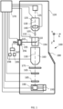
FIG. 1 depicts a microscopy system that can incorporate detectors of the present disclosure. -
FIG. 2 depicts a cross section of a detector for microscopy. -
FIG. 3 depicts a cross section of a detector incorporating an extension according to the present disclosure. -
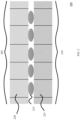
FIGS. 4A and4B depict top perspective views of a detector according to the present disclosure. -
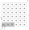
FIG. 5 depicts a top perspective view of a detector. -
FIG. 6 depicts a top perspective view of a detector according to the present disclosure. -
FIG. 7 depicts a top perspective view of a detector according to the present disclosure. -
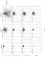
FIG. 8 depicts interaction volume graphs for various compositions. -
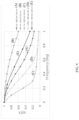
FIG. 9 depicts a graph for exemplary, non-limiting MTF and DQE(0) values for various compositions. -
FIG. 10 depicts interaction volume graphs for various compositions. -
FIG. 11 depicts a top perspective view of a detector. -
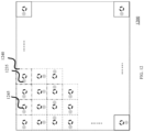
FIGS. 12-16 depict a detector with various numbers of sensing pixels incorporated onto an electronic layer, according to the present disclosure. -
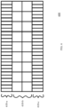
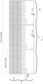
FIG. 17 depicts a sensor array according to the present disclosure. -
FIG. 18 depicts a sensor array according to the present disclosure. - The present disclosure may be understood more readily by reference to the following detailed description taken in connection with the accompanying figures and examples, which form a part of this disclosure. It is to be understood that this invention is not limited to the specific devices, methods, applications, conditions or parameters described and/or shown herein, and that the terminology used herein is for the purpose of describing particular embodiments by way of example only and is not intended to be limiting of the claimed invention. Also, as used in the specification including the appended claims, the singular forms "a," "an," and "the" include the plural, and reference to a particular numerical value includes at least that particular value, unless the context clearly dictates otherwise. The term "plurality", as used herein, means more than one. When a range of values is expressed, another embodiment includes from the one particular value and/or to the other particular value. Similarly, when values are expressed as approximations, by use of the antecedent "about," it will be understood that the particular value forms another embodiment. All ranges are inclusive and combinable, and it should be understood that steps can be performed in any order. Any documents cited herein are incorporated by reference in their entireties for any and all purposes.
- It is to be appreciated that certain features of the invention which are, for clarity, described herein in the context of separate embodiments, can also be provided in combination in a single embodiment. Conversely, various features of the invention that are, for brevity, described in the context of a single embodiment, can also be provided separately or in any subcombination. Further, reference to values stated in ranges include each and every value within that range. In addition, the term "comprising" should be understood as having its standard, open-ended meaning, but also as encompassing "consisting" as well. For example, a device that comprises Part A and Part B can include parts in addition to Part A and Part B, but can also be formed only from Part A and Part B.
- Turning to
FIG. 1, FIG. 1 depicts amicroscopy system 100, particularly a transmission electron microscopy (TEM)system 100 configured to use anelectron beam 105 to observe and/or characterize asample 110.Microscopy system 100 can acquire an image of thesample 110 using the emissions in the transmission region of themicroscopy system 100. Thus,system 100 can represent a Transmission Electron Microscope (TEM) or a Scanning Transmission Electron Microscope (STEM). - Within a
vacuum enclosure 120, anelectron source 125 can produce thebeam 105 of electrons that propagates along an electron-optical axis 130 and traverses an electron-optical illuminator 135, serving to direct/focus the electrons onto a chosen part of thesample 110 positioned insample chamber 194.Sample 110 can be, e.g., be (locally) thinned/planarized or otherwise processed for analysis. - Also depicted is a
deflector 140, which can, inter alia, be used to effect scanning motion of thebeam 105. Thesample 110 can be held on asample holder 145 that can be positioned in multiple degrees of freedom by agoniometer 196. For example, thesample 110 can be positioned in a holder capsule of the sample holder that can be moved (inter alia) in the XY plane (see the depicted Cartesian coordinate system; typically, motion parallel to Z and tilt about X/Y will also be possible). Such movement allows different parts of thesample 110 to be illuminated / imaged / inspected by theelectron beam 105 traveling along axis 130 (in the Z direction) (and/or allows scanning motion to be performed, as an alternative to beam scanning). If desired, an optional cooling device (not depicted) can be brought into intimate thermal contact with thesample holder 145, so as to maintain it (and thesample 110 thereupon) at cryogenic temperatures, for example. The holder capsule of the sample holder can be sealable, so that the sample can be transferred into and out of the TEM under vacuum or inert gas. - The
electron beam 105 can interact with thesample 110 in such a manner as to cause various types of "stimulated" radiation to emanate from thesample 110, including (for example) secondary electrons, backscattered electrons, X-rays and optical radiation (cathodoluminescence). If desired, one or more of these radiation types can be detected with the aid ofanalysis device 155, which might be a combined scintillator/photomultiplier or EDX (Energy-Dispersive X-Ray Spectroscopy) module. However, alternatively or supplementally, one can study electrons that traverse (pass through) thesample 110, exit/emanate from thesample 110, and continue to propagate (substantially, though generally with some deflection/scattering) alongaxis 130. - Such a transmitted electron flux enters an imaging system (projection lens) 160, which can comprise a variety of electrostatic / magnetic lenses, deflectors, correctors (such as stigmators), and the like. In normal (non-scanning) TEM mode, this
imaging system 160 can focus the transmitted electron flux. Various types of analysis apparatus can be used downstream ofimaging system 160, such as aTEM camera 165. Atcamera 165, the electron flux can form a static image (or diffractogram) that can be processed by controller/processor 170 and displayed on a display device (not depicted), such as a flat panel display, for example. When not required,camera 165 can be retracted/withdrawn so as to get it out of the way ofaxis 130. Alternatively, or additionally, theimaging system 160 can be used to focus the transmitted electron flux onto afluorescent screen 175, which, if desired, can be retracted/withdrawn so as to get it out of the way ofaxis 130. An image (or diffractogram) of (part of) thesample 110 will be formed byimaging system 160 onscreen 175, and this can be viewed through viewingport 180. - An analysis apparatus can also include a
STEM camera 185. An output fromcamera 185 can be recorded as a function of (X,Y) scanning position of thebeam 105 on thesample 110, and an image can be constructed that is a "map" of output fromcamera 185 as a function of X,Y.Camera 185 can include a single pixel with a diameter of e.g. 20 mm, as opposed to the matrix of pixels characteristically present incamera 165. Moreover,camera 185 will generally have a much higher acquisition rate (e.g., 106 points per second) than camera 165 (e.g., 102 - 103 images per second). Once again, when not required,camera 185 can be retracted/withdrawn so as to get it out of the way ofaxis 130. - As an alternative to
imaging using cameras spectroscopic apparatus 190, which could be an Electron Energy Loss Spectroscopy (EELS) module, for example. Theapparatus 190 can include adetector 193, which can be an EELS sensor array. A sensor array can include a sensing layer and an electronic layer, which is described in more detail below. It should be noted that the order/location ofitems spectroscopic apparatus 190 can also be integrated into theimaging system 160. - The
controller 170 is connected to various illustrated components via control lines (buses). The controller includes at least a processor as well as a non-transitory memory for storing computer readable instructions. By executing the computer readable instructions in the processor, thiscontroller 170 can provide a variety of functions, such as synchronizing actions, providing setpoints, processing signals, performing calculations, and displaying messages/information on a display device (not depicted). The controller can be configured to implement some or all steps of the methods described herein. Thecontroller 170 can be (partially) inside or outside theenclosure 120, and can have a unitary or composite structure, as desired. - The
goniometer 196 can position the sample under the electron beam within a vacuum chamber of the microscope. The vacuum chamber can be asample chamber 194. The sample can be imaged or processed with the charged particle beams in the sample chamber. Thegoniometer 196 can be coupled withenclosure 120. The goniometer can include one or more actuation mechanisms for tilting the sample around one or more tilt axes. - The
goniometer 196 includes aload lock 195 to facilitate the transfer ofsample 110 from external to themicroscopy system 100 to within the sample chamber. Theload lock 195 can include ingress/egress points for thesample 110 to transition from the external of the TEM to theload lock 195, and from theload lock 195 to the sample chamber of the microscope column. For example, theload lock 195 can include an opening at one end for receiving a sample holder from the external of TEM. The load lock can be sealable from the external environment via one or more O-rings. Similarly, theload lock 195 can also include an opening on another end (e.g. opposite end) for passing the sample held by the sample holder from theload lock 195 to the sample chamber of the microscope. The opening between the load lock and the sample chamber is sealable via a valve. Thus, when thesample 110 is positioned within the load lock 195 (via the sample holder), the environment of load lock can be substantially isolated from sample chamber. - The
goniometer 196 can include agas delivery train 197 to place the chamber into interruptible fluid communication with both a protectingsource 198 and with avacuum pump 199. Theload lock 195 can be coupled with one or more gas sources and pumps via valves for controlling the gas flow into and out of theload lock 195. In one example, the load lock can be fluidically connected to avacuum pump 199 via a first valve and fluidically connected to a protectinggas source 198 via a second valve. The valves can be open or closed by actuation respective actuators controlled by thecontroller 170. - Any or all of the sensors discussed with regards to
FIG. 1 , such asTEM camera 165,STEM camera 185, and/ordetector 193, may be formed from a sensing layer electrically coupled to a readout/control layer via respective contacts. In such examples, the sensing layer may have a plurality of pixels coupled to respective electronics in the readout/control layer. Such electrical connection(s) can connect pixels having a different shape and/or orientation than the associated electronics. In some examples, the pixels may extend across multiple areas of un-associated electronics. Additionally, some examples may have different sensors formed from different materials, where the different materials are tuned to different electron energies. - The TEM system can include other type of transmission electron microscopy system such as a scanning transmission electron microscope. In some examples, the TEM system can include another charged particle column such as an ion column.
-
FIG. 2 depicts a cross-sectional view of asensor 200 that can be implemented in a charged particle microscopy system, such asmicroscopy system 100 ofFIG. 1 (e.g., detector 193). Thesensor 200 can include asensing layer 205 and anelectronic layer 210. Thesensing layer 205 can include a plurality of sensingpixels 220, which can be oriented in a plane. Theelectronic layer 210 can include a pluralityelectronic units 225, which can be oriented in a plane parallel to the plane of thesensing layer 205. The planes of thesensing layer 205 and theelectronic layer 210 can define width and length directions. - The
sensor layer 205 can include a composition capable of transporting captured charged particles through the thickness of thesensing pixel 220. For example, compositions can include silicon (Si), cadmium telluride (CdTe), cadmium zinc telluride (CdZnTe), and gallium arsenide (GaAs). A given composition can be more effective at transporting captured charged particles based on a particular energy range of the charged particles. For example,FIG. 10 depicts interaction volume graphs for various compositions. The graphs depict emission interactions, such as electron emissions from the TEM, with various substrates. The first row of graphs depicts interaction volumes for 150 µm Si layered on a CdTe substrate. The second row of graphs depicts interaction volumes for 20 µm Si and 100 µm of CdTe. The third row of graphs depicts interactions volumes for 55 µm Si layered on 100 µm of CdTe. The fourth row of graphs depicts interactions volumes for 150 µm of CdTe. - The
electronic layer 210 can include electronics capable of receiving an electronic signal from thesensing layer 205, and to relay the electronic signal to other electronic components to the microscopy system, such as a processor or memory of the microscopy system. For example, eachelectronic unit 225 can include a readout cell that is electrically coupled to one of the sensingpixels 220. While thesensing layer 205 andelectronic layer 210 can provide for a 1:1 ratio between respective sensingpixels 220 and electronic units 225 (e.g., where eachsensing pixel 220 is electrically coupled to a respectiveelectronic unit 225, or where each sensing pixel profile is equivalent to, and centered on, a respective electronic unit profile), the disclosure provided herein can allow for differences in profiles between a sensing pixel and respective electronic unit, an offset between sensing pixel profile and respective electronic unit profile, and the like, which will be discussed in more detail below. - In some cases, the
electronic layer 210 can form an application-specific integrated circuit (ASIC), or can be a part of an ASIC. Theelectronic layer 210 can define a plane along a width and length dimension of the layer., such that the plane of theelectronic layer 210 is substantially parallel to the plane defined by thesensing layer 205. - The
sensor 200 can also include a bump bonds 215. The bump bond can provide an electrical contact between thesensing layer 205 and theelectronic layer 210. Thebump bond 215 can be composed of a composition having high electrical conductivity, such as a metal. Typically, a bump bond contacts a center portion of asensing pixel 220 and a center portion of an associatedelectronic unit 225, though this is not a requirement. -
FIG. 3 depicts a cross-sectional view of asensor 300 according to the present disclosure. The sensor can be implemented in a microscopy system, such asmicroscopy system 100 ofFIG. 1 . Thesensor 300 includes asensing layer 205 having one ormore sensing pixels 220, anelectronic layer 210 having one or moreelectronic units 225, abump bond 215, and may further include anextension 320. Theextension 320 can extend parallel to the planes defined by thesensing layer 205 and theelectronic layer 210. In general, theextension 320 provides an electrical path that couples thebump bond 215 to thesensing pixel 220 that allows thesensing pixel 220 and theelectronic unit 225 to be offset from one another in one or more dimensions. Additionally,extension 320 also allows for a shape and size of asensing pixel 220 to be different than a shape and size of the associatedelectronic unit 225. In some examples, amember 325 can connectsensing pixel 220 toextension 320. Theextension 320 andmember 325 can also be composed of an electrically conductive material, such as a metal. Theextension 320, throughmember 325, can couple thesensing pixel 220 with the electronic unit 225 (via the bump bond 215) when their respective geometries and locations are not similar. For example, where the center portion of thesensing pixel 220 and the center portion of theelectronic unit 225 are adjacent to each other (e.g., along the center axis), theextension 320 can couple a region apart from the center portion of thesensing pixel 220 with the center portion of theelectronic unit 225. In cases where thesensing pixel 220 does not align with the electronic unit 225 (e.g., along the center axis), theextension 320 can allow for the center portion of thesensing pixel 220 to be coupled to the center portion of theelectronic unit 225. -
FIG. 4A and4B depicts a detector 400-a, 400-b that can be implemented in a charged particle microscopy system, such asmicroscopy system 100 ofFIG. 1 (e.g., detector 193). The detector 400-a, 400-b can include a plurality ofelectronic units 225, and a configuration of sensingpixels 220 coupled toelectronic units 225 viabump bonds 215,extensions 320, andmembers 325. As shown inFIG. 4A and4B , a sensing pixel (220) can be elongate in configuration, as opposed to a square pixel. In this way, the disclosed technology allows one to construct a device in which a pixel need not be the same size/shape as an associated electronic unit, which capability allows a user to utilize differently-shaped pixels depending on the user's needs. WhileFIG. 4A and4B show three sensing pixels extending across three electronic units, such number and relationship is not limiting. For example, in some examples, 4 or more pixels may extend across 4 or more electronic units with similar connections as shown where a size of the sensors in one direction is reduced to accommodate the additional sensing pixels. Likewise, the angle and direction in which theextension 320 extends from thebump bond 215 can vary as well. For example,FIG. 4A depictsextensions 320 extending away from acorresponding bump bond 215 such that a length of theextension 320 is aligned with a width or length dimension of the detector 400-a. As another example,FIG. 4B depicts someextensions 320 extending away from acorresponding bump bond 215 offset from either the length or width dimensions of the detector 400-b (e.g., 45 degrees from the detector width/length dimension). - As mentioned, sensing pixels for the sensors described herein can be of different shapes, sizes, and the like, compared to the corresponding electronic unit to which the sensing pixel is electrically coupled to. For example, an electronic unit can be generally square in shape. A corresponding sensing pixel coupled to the electronic unit can be rectangular in shape (as depicted in
FIG. 4A ,4B ). However, the shape of the sensing pixel can be a variety of shapes. For example, the sensing pixel can be a square, a rectangle, a circle or oval, a polygon, an ellipse, a crescent, a polyomino, and the like. Likewise, the shape of the corresponding electronic unit can vary as well, and is not limited to the square shapes depicted inFIG. 4A ,4B . - In some cases, the dimensions of the sensing pixel can differ from that of the corresponding electronic unit. For example, a sensing pixel can define length and width dimensions, which can form a profile of the sensing pixel. Likewise, the corresponding electronic unit can define length and width dimensions, which can form a profile of the electronic unit. In some cases, the profile of the sensing pixel can differ from that of the corresponding electronic unit. For example the length or width, or both, of the sensing pixel can be different than the length or width of the corresponding electronic unit. Thus, in some cases, the sensing pixel can include a shape similar to that of the electronic unit; however, the size of the sensing pixel can be different than the corresponding electronic unit (due to the differences in dimensions). In some cases, the area of the sensing pixel can be equivalent to the area defined by the corresponding electronic unit. In some other cases, the area of the sensing pixel can differ than the area defined by the corresponding electronic unit.
- In some cases, the profile of a sensing pixel can be offset from the profile of the corresponding electronic unit. For example, a sensing pixel can be oriented such that a profile does not entirely match the profile of the corresponding electronic unit. For example, when viewed in the thickness direction (such as in
FIG. 4A ,4B ), the profile of a sensing pixel does not entirely cover the profile of the corresponding electronic unit, or that a portion of the profile of the sensing pixel does not overlap with the profile of the corresponding electronic unit in the thickness direction (or vice versa). In some cases, edges or corners of a sensing pixel can be non-adjacent to respective edges or corners of a corresponding electronic unit when viewed in the thickness direction (e.g., a sensing pixel rotated 45 degrees with respect to the corresponding electronic unit). -
FIG. 5 depicts anelectronic layer 500 for a sensor according to the present disclosure.FIG. 5 depicts a top view of theelectronic layer 500 which can include a plurality ofelectronic units 225. Theelectronic units 225 can generally be 2-dimensional, such that theelectronic unit 225 can define a length and width, and the thickness is substantially smaller than the length and width. Theelectronic units 225 can be arranged such that a side of an electronic unit can be adjacent to, or contact a side of another electronic unit. In this fashion, theelectronic layer 500 can define a 2-dimensional plane. Theelectronic units 225 can be generally uniform in nature, such that a profile of an electronic unit can equate to other electronic units of theelectronic layer 500. In some cases, theelectronic units 225 can be dimensioned as a square. Theelectronic units 225 can be arranged such that the electronic units form theprofile 505 outlined inFIG. 5 . - For electron energy loss spectroscopy (EELS), the dimensions and composition of the sensing layer can affect how well the sensing layer captures charged particles within a given energy range. For electron energies below 100 keV, Si with small dimensions (e.g., pixel size) can be effective (e.g., having high detective quantum efficiency (DQR) and modular transfer function (MTF) values). While CdTe and GaAs can also be used at small dimensions, those material systems can have lower DQE values with respect to Si. At electron energies greater than 200 keV, CdTe at smaller dimensions can be effective. Electron energies between 100 and 200 keV, Si having large dimensions can be effective (See, e.g.,
FIG. 9 for example MTF values for different sensing layer sizes and compositions). Further, Si can include DQE(0) values above 0.9. For GaAs, CdTe, and CdZnTe the DQE(0) can be between 0.6 and 0.8 at 300 keV, and between 0/4 and 0.7 at 100 keV. For MTF values, at pixel size of 50 µm, Si can be 0.1 at 100 keV, and 0.3 for CdTe at 100 keV. - Thus, to capture charged particles across a wide range of energies, such as from 0 to 300 keV, different compositions and different dimensions of sensing pixels can be included in the sensing layer, while keeping conventional electronic unit dimensions of a corresponding electronic layer the same.
FIG. 6 depicts asensor array 600 for microscopy systems according to the present disclosure. Thesensor array 600 can be a sensor, such assensor 200 ofFIG. 2 . In some cases, thesensor array 600 can be an aggregation of sensors, such as threesensors 200 disposed side-by-side to form the sensor array. Thesensor array 600 can include a sensing layer including a plurality of sensing pixels, and having sensing layer rows 610-a. 610-b, and 610-c. Row 610-a can include a first composition, row 610-b can include a second composition, and row 610-c can include a third composition. In some cases, the compositions can include Si, CdTe, or GaAs, respectively. In some cases, the dimensions for the sensing pixels of the rows 610-a-c can vary and need not be the same as the underlying electronic readout unit. For example, the width of a sensing pixel in row 610-a can be smaller than the width of a sensing pixel in row 610-b. Thus, for the width of thesensor array 600, there can be more sensing layers (e.g., pixels) in a given row (e.g., row 610-a) compared to another row (e.g., 610-b). Thesensor array 600 can thus include different sensing pixel types, which can increase the effectiveness of thesensor array 600 in capturing charged particles across a wider range of energies. - The
sensor array 600 can also include an electronic layer (not shown). The electronic layer can include a plurality of electronic units such as those described above with reference toFIG. 2 , where for example, each electronic unit includes a chip readout for receiving electrical measurements from a corresponding sensing pixel. The dimensions of each electronic unit can be uniform throughout, such that an electronic unit corresponding to a sensing layer of row 610-a can include the same dimensions as an electronic unit corresponding to row 610-b. For example, the dimensions of an electronic unit can match the dimensions of a sensing pixel in row 610-b (e.g., such that a sensing pixel of row 610-b sits on top of the corresponding electronic unit, and a center portion of the sensing pixel is coupled to a center portion of the electronic unit). In cases where a sensing pixel is offset from the corresponding electronic unit, a bump bond and extension can electrically couple the layers. -
FIG. 7 depicts asensor array 700 for microscopy according to the present disclosure. Thesensor array 700 can include an aggregated sensing layer having sensing layer row 710-a and sensing layer rows 710-b. Row 710-a can include a first composition, and rows 710-b can include a second composition (e.g., Si). In some cases, the first composition can include layered compositions, such as Si layered on top of, or the bottom of, CdTe. This layered composition can utilize the benefits of the variety of compositions included therein. For example, a layered composition can include a 50 µm thick layer of Si positioned on top of a layer of CdTe. The Si can absorb energy below 100 keV, and the CdTe can reduce interaction volume for charged particles with energy between 200-300 keV. This layered composition can thus reduce backscattering, which can provide a higher DQE value compared to a layer of CdTe.FIG. 8 depicts interaction volumes for various sensing pixel configurations according to the present disclosure.FIG. 8 depicts a 50 µm layer of Si interacting with electron emissions having less than 100 keV of energy; a 50 µm layer of Si on top of a CdTE substrate interacting with electron emissions having 300 keV of energy; and a 50 µm layer of Si on top of a Si substrate interacting with electron emissions having 300 keV of energy. As shown inFIG. 8 , the CdTe substrate composition reduces backscattering of electron emissions at 300 keV compared to the backscattering experienced by the Si-only pixel composition at 300 keV energy. An example of this layered sensor array can be found inFIG. 18 , where a first sensing layer is layered on a second sensing layer, second layer is layered on a third sensing layer, third sensing layer is layered on fourth sensing layer, and fourth sensing layer is layered on an electronic unit layer (e.g., which can include a number of ASICs). -
FIG. 11 depicts a top view of asensor array 1100 for microscopy systems.FIG. 11 illustrates acontact region 1135 for eachsensing pixel 1110, where eachsensing pixel 1110 is electrically coupled to a corresponding electronic unit. In this configuration, thecontact region 1135 can be adjacent to a contact region of a corresponding electronic unit (e.g., thecontact region 1135 aligns with the contact region of the corresponding electronic unit positioned below the sensing pixel). In short,Fig. 11 shows a 1 to 1 relationship in terms of shape and size between the sensing pixels and associated electronic units. -
FIG. 12 depicts a top view of asensor array 1200.FIG. 12 illustratescontact regions 1235 of a sensing layer of sensing pixels with respect to a corresponding electronic unit (as shown with dashed lines 1240). As can be seen, thecontact regions 1235 do not align with a contact region of a corresponding electronic unit. Thus, in cases where the contact region of the sensing layer is electrically coupled to thecontact region 1245 of the electronic unit, an extension (e.g., extension 320) can be utilized between the sensing layer and electronic unit. -
FIGS. 13-16 illustrate thesensor array 1200 with additional sensing pixels incorporated. For example,FIG. 13 illustrates a sensing pixel 1310-a positioned with respect to the electronic layer. The sensing pixel 1310-a can be coupled at contact region 1335-a, to electronic unit 1305-a. The contact region for the electronic unit 1310-a can be within a center area of the electronic unit 1310-a and thus the contact region 1335-a and the contact region for the electronic unit 1310-a are not aligned. Thus, an extension (e.g.,extension 320 ofFIG. 3 ) can electrically couple the sensing pixel 1305-a to the electronic unit 1310-a (e.g., via a bump bond) by extending between contacts of the pixel 1305-a and the electronic unit 1310-a. In some cases, a member (e.g.,member 325 ofFIG. 3 ) can also be utilized to couple the extension to the sensing pixel). As can be seen, the dimensions of the sensing pixel 1305-a can be different than the dimensions of the electronic unit 1310-a. For example, the sensing pixel 1305-a can be three times smaller in the width dimension compared to the width of the electronic unit 1310-a, whereas the sensing pixel 1305-a can be three times as large in the length dimension compared to the length of the electronic unit 1310-a.FIG. 14 illustrates a second sensing pixel 1305-b coupled to an electronic unit 1310-b, andFIG. 15 illustrates a third sensing layer 1305-c coupled to an electronic unit 1310-c. As can be seen, the contact region 1035-a-c for each sensing layer 1305-a-c can differ with respect to a contact region for a corresponding electronic unit 1310-a-c. For example, the positioning of the contact region 1335-a can be a 90 degree clockwise shifted with respect to the contact region 1335-b (with respect to the contact region of the corresponding electronic unit 1310-a and b). Thus, the positioning of the contact regions with respect to the corresponding electronic unit can form a pattern (e.g., 90 degree clockwise shifted, 90 degree counter-clockwise shifted, 180 degree shifted, and the like), along a given dimension of the sensor array 1200 (e.g., length or width). This pattern can be further seen inFIG. 15 . - Thus sensing layers having different dimensions compared to their respective electronic units can be implemented. By altering the dimensions of the sensing layer (e.g., the sensing pixel shapes and sizes) with respect to the electronic unit, a number of sensing pixels along a given sensor array dimension can be increased or decreased. For example,
FIG. 17 depicts asensor array 1700 according to the present disclosure. Thesensor array 1700 can include an electronic layer, which can include, for example, one or more ASICs (e.g., ASICS 1710-a-c). The electronic layer can include a number of electronic units along the width dimension, such as 384 electronic units, and a number of electronic units along the length dimension, such as 128 electronic units. Thesensor array 1700 can also include an aggregated sensing layer, which can include a number of sensing pixels along thewidth dimension 1740, such as 1,152 sensing pixels, and a number of sensing pixels along thelength dimension 1745, such as 14. Thesensor array 1700 can thus be configured for particular EELS detections while maintaining an electronic layer that can be configured for different detections. - As a particular non-limiting example, an Electron Microscope Pixel Array Detector (EMPAD) can include a 150 µm electronic unit (e.g., ASIC) can be utilized, along with a differently dimensioned sensing pixel layer. The sensing pixel dimensions can be include 450 µm in length and 50 µm in width. Thus, on a 150 µm x 150 µm electronic unit, 384 sensing pixels can be positioned in the width dimension. By tiling 3 electronic units together (e.g., side by side), 1,152 pixels can be positioned in the width direction, and 14 pixels in the length direction. With a frame rate of 10,000 frames per second, this configuration can enable the capturing of 100,000 spectra per second.
- The following embodiments are exemplary only and do not serve to limit the scope of the present disclosure of the appended claims. It should be understood that any part of any one or more Embodiments can be combined with any part of any other one or more Embodiments.
- A sensor, comprising: an electronic layer configured to receive and send electronic signals, the electronic layer defining a first dimension measured along a first direction and a second dimension measured along a second direction; and a sensing layer coupled to the electronic layer, the sensing layer defining a first dimension measured along the first direction and a second dimension measured along the second direction, and (a) the first dimension of the electronic layer differing from the first dimension of the sensing layer, (b) the second dimension of the electronic layer differing from the second dimension of the sensing layer, or both (a) and (b).
- The sensor of
Embodiment 1, wherein at least one of the first dimension and the second dimension comprises a length or a width. - The sensor of any one of
Embodiments 1 through 2, wherein the electronic layer comprises an ASIC. - The sensor of any one of
Embodiments 1 through 3, wherein the sensing layer is configured to: receive a charged particle, convert the charged particle to an electronic signal; and send the electronic signal to the electronic layer via a coupling between the electronic layer and the sensing layer. - The sensor of any one of
Embodiments 1 through 4, wherein a coupling between the sensing layer and the electronic layer comprises a bump bond, the coupling optionally comprising at least one via placing the bump bond in electronic communication with the sensing layer. - The sensor of any one of
Embodiments 1 through 5, wherein each of the sensing layer and the electronic layer define a center point, and wherein (a) a portion of the sensing layer other than the center point is coupled to the center point of the electronic layer or (b) a portion of the electronic layer other than the center point is coupled to the center point of the sensing layer. - The sensor of any one of
Embodiments 1 through 6, wherein the sensing layer and the electronic layer each define a plane, wherein each plane is parallel with the other. - The sensor of any one of
Embodiments 1 through 7, wherein a coupling between the electronic layer and the sensing layer comprises a portion that extends in parallel with the electronic layer plane and the sensing layer plane. - The sensor of any one of
Embodiments 1 through 8, wherein a perimeter profile of the sensing layer is different than a perimeter profile of the electronic layer. - The sensor of any one of
Embodiments 1 through 9, wherein the perimeter profile of the electronic layer comprises a square. - The sensor of any one of
Embodiments 1 through 10, wherein the perimeter of the sensing layer comprises a rectangle or a polyomino. - The sensor of any one of
Embodiments 1 through 11, wherein the sensor is configured for electron energy loss spectroscopy (EELS). - The sensor of any one of
Embodiments 1 through 12, wherein the electronic layer is 150µm x 150µm, and wherein the sensing layer has a width of 50 µm. - A sensor array for spectroscopy, comprising: a plurality of the sensor of any of Embodiments 1-13, wherein the plurality of the sensing layers defines an aggregated sensing layer, and the plurality of the electronic layers defines an aggregated electronic layer, the sensor array defining a plane.
- A sensor array of
Embodiment 14, wherein the aggregated electronic layer further comprises at least one electronic layer free of coupling to a sensing layer. - A sensor array of any of
Embodiments 14 through 15, wherein the aggregated sensing layer comprises 128 sensing layers arranged along a first direction in the plane of the aggregated sensing layer. - A sensor array of any of
Embodiments 14 through 16, wherein the aggregated sensing layer comprises at least two sensing layers arranged along a second direction in the plane of the aggregated sensing layer. - A sensor array of any of
Embodiments 14 through 17, wherein the plurality of couplings comprises a coupling pattern defining a plurality of coupling locations, and (i) wherein within the coupling pattern a first coupling of the plurality of couplings is coupled to a first sensing layer at a first location located at a first distance measured along a direction parallel to the plane, (ii) wherein a second coupling is coupled to a second sensing layer at a location located at a second distance measured along the direction, and (iii) wherein the first distance differs from the second distance. - A sensor array of any of
Embodiments 14 through 18, wherein a first coupler of the plurality of couplings extends in a first direction parallel to the plane, wherein a second coupler of the plurality of couplings extends in a second direction parallel to the plane, and wherein the first direction differs from the second direction. - A sensor array of any of
Embodiments 14 through 19, wherein the coupling locations of a plurality of the electronic layers are arranged in a substantially periodic manner. - A sensor array, comprising: an electronic layer comprising a plurality of electronic units configured to receive and send electronic signals, the electronic layer optionally comprising an ASIC, the electronic layer defining a first dimension measured along a first direction and a second dimension measured along a second direction, wherein the electronic layer further defines a plurality of rows of the electronic units, and wherein each row of the plurality of rows optionally spans either the first dimension or the second dimension; a first sensing layer comprising a plurality of first sensing pixels composed of a first material, wherein a first sensing pixel is coupled to a respective electronic unit of the plurality of electronic units; and a second sensing layer comprising a plurality of second sensing pixels composed of a second material that differs from the first material, and wherein each of the second sensing pixels is coupled to a respective electronic unit of the plurality of electronic units.
- A sensor array of Embodiment 21, wherein a first sensing pixel or a second sensing pixel is composed of silicon (Si).
- A sensor array of any of Embodiments 21 through 22, wherein a first sensing pixel or a second sensing pixel is composed of cadmium telluride (CdTe) or gallium arsenide (GaAs).
- A sensor array of any of Embodiments 21 through 23, wherein a first subset of the plurality of rows is comprised of the first sensing layer, and wherein a second subset of the plurality of rows is comprised of the second sensing layer.
- A sensor array of any of Embodiments 21 through 24, wherein each of the first sensing pixels and the second sensing pixels are configured to: receive a charged particle, convert the charged particle to an electronic signal; and send the electronic signal to the electronic layer via a coupling between (i) a respective sensing pixel of either the plurality of first sensing pixels or of the plurality of second sensing pixels, and (ii) a corresponding electronic unit of the plurality of electronic units.
- A sensor array of any of Embodiments 21 through 25, wherein the first sensing layer is configured to convert a charged particle of a first energy level range to an electronic signal; and wherein the second sensing layer is configured to convert a charged particle of a second energy level range to an electronic signal, wherein the first energy level range and the second energy level range are different.
- A sensor array of any of Embodiments 21 through 26, wherein the first energy level range comprises less than 100 keV, between 100keV and 200 keV, and greater than 200 keV.
- A sensor array of any of Embodiments 21 through 27, wherein a first sensing pixel defines a different perimeter shape than a perimeter shape of a second sensing pixel.
- A sensor array of any of Embodiments 21 through 28, wherein the plurality of first sensing pixels defines a total number of first sensing pixels, wherein the plurality of second sensing pixels defines a total number of second sensing pixels, and wherein the first number differs from the second number.
- A sensor array of any of Embodiments 21 through 29, wherein each of a first sensing pixel of the plurality of first sensing pixels and each of an electronic unit of the plurality of electronic units define a third dimension measured along the first direction and a fourth dimension measured along the second direction, and (a) the third dimension of the electronic unit is the same as the third dimension of the first sensing pixel, (b) the third dimension of the electronic unit differs from the third dimension of the first sensing pixel, (c) the fourth dimension of the electronic unit is the same as the fourth dimension of the first sensing pixel (d) the fourth dimension of the electronic unit differs from the fourth dimension of the first sensing pixel, or a combination thereof.
- A sensor array of any of Embodiments 21 through 30, further comprising a third sensing layer composed of the first material, and comprising a plurality of third sensing pixels, wherein each of the third sensing pixels is coupled to a respective electronic unit; and wherein a perimeter profile shape of a first sensing pixel differs from a perimeter profile shape of a third sensing pixel.
- A sensor array of any of Embodiments 21 through 31, wherein the electronic layer lies in a plane and a line extending orthogonally from the plane passes through a first sensing pixel and through a second sensing pixel, and wherein the first sensing pixel is coupled to the second sensing pixel, the second sensing pixel being coupled to an electronic unit of the electronic layer.
- A sensor array of any of Embodiments 21 through 32, wherein the first sensing layer is configured to convert a charged particle of a first energy level range to an electronic signal; and wherein the third sensing layer is configured to convert a charged particle of a second energy level range to an electronic signal, wherein the first energy level range and the second energy level range are different.
- A sensor array of any of Embodiments 21 through 33, wherein the perimeter profile shape of each of the first sensing pixels is a rectangle, and wherein the perimeter profile shape of each of the third sensing layers is a square.
- A sensor array of any of Embodiments 21 through 34, wherein the sensor array is configured for electron energy loss spectroscopy (EELS).
- A sensor array of any of Embodiments 21 through 35, wherein the electronic layer lies in a plane and a first line extending orthogonally from the plane passes through a first sensing pixel without passing through a second sensing pixel, and wherein a second line extending orthogonally from the plane passes through a second sensing pixel without passing through a first sensing pixel.
- A sensor array of any of Embodiments 21 through 36, wherein a coupling between a respective first sensing pixel of the plurality of first sensing pixels, and a corresponding electronic unit of the plurality of electronic units comprises a bump bond, the coupling optionally comprising at least one via placing the bump bond in electronic communication with the first sensing layer.
- A sensor array of any of Embodiments 21 through 37, wherein each a first sensing pixel of the plurality of first sensing pixels and an electronic unit of the plurality of electronic units define a center point, and wherein (a) a portion of the first sensing pixel other than the center point is coupled to the center point of the electronic layer or (b) a portion of the electronic unit other than the center point is coupled to the center point of the first sensing pixel.
- A sensor array of any of Embodiments 21 through 38, wherein the first sensing layer and the second sensing layer define a first plane, and the electronic layer defines a second plane, wherein the first plane and the second plane are parallel with each other.
- A sensor array of any of Embodiments 21 through 39, wherein a coupling between a first sensing pixel and the corresponding electronic unit comprises a portion that extends in parallel with the first plane and the second plane.
- An apparatus comprising: a plurality of electronic units arranged in an array; a plurality of pixels, each pixel of the plurality of pixels coupled to an associated electronic unit of the plurality of electronic units, wherein a first subset of pixels of the plurality of pixels is formed from a first material, and wherein a second subset of pixels of the plurality of pixels is formed from a second material, the first material being different than the first material, and a plurality of electrical connections disposed between the plurality of electronic units and the plurality of pixels, where each electrical connection connects its respective electronic units with an associated pixel.
- The apparatus of Embodiment 41, wherein the first material is silicon (Si), and the second material is cadmium telluride (CdTe).
- The apparatus of any of Embodiments 41 through 42, wherein at least one of the first material and the second material is formed from stacking a plurality of layers.
- The apparatus of any of Embodiments 41 through 43, wherein each pixel of the first subset of pixels has a different shape than its associated electronic unit.
- The apparatus of any of Embodiments 41 through 44, wherein each pixel of the first subset of pixels has a different size than it associated electronic unit.
- The apparatus of any of Embodiments 41 through 45, wherein each pixel of the first subset of pixels extends across multiple electronic units in at least one direction.
- The apparatus of any of Embodiments 41 through 46, wherein each pixel of the first subset of pixels has a different shape than each pixel of the second subset of pixels.
- An apparatus comprising: a plurality of electronic units arranged in an array; a plurality of pixels, each pixel of the plurality of pixels coupled to an associated electronic unit of the plurality of electronic units, wherein each pixel of a first subset of pixels of the plurality of pixels defines a shape that is different than a shape of an associated electronic unit, and a plurality of electrical connections disposed between the plurality of electronic units and the plurality of pixels, wherein each electrical connection connects respective electronic units with an associated pixel.
- The apparatus of Embodiment 48, wherein the shape of the first subset of pixels comprises a rectangle, and the shape of the associated electronic units comprises a square.
- The apparatus of any of Embodiments 48 through 49, wherein the first subset of pixels is a first material and a second subset of pixels is a second material that is different than the first material.
- The apparatus of any of Embodiments 48 through 50, wherein the first material is silicon (Si), and the second material is cadmium telluride (CdTe).
- The apparatus of any of Embodiments 48 through 51, wherein each pixel of the first subset of pixels has a different size than its associated electronic unit.
- The apparatus of any of Embodiments 48 through 52, wherein each pixel of the first subset of pixels extends across multiple electronic units in at least one direction.
- The apparatus of any of Embodiments 48 through 53, wherein the first subset of pixels is configured to convert a charged particle of a first energy level range to an electronic signal; and wherein a second subset of pixels of the plurality of pixels is configured to convert a charged particle of a second energy level range to an electronic signal, wherein the first energy level range and the second energy level range are different.
- An apparatus comprising: a plurality of electronic units arranged in an array; a plurality of pixels, each pixel of the plurality of pixels coupled to an associated electronic unit of the plurality of electronic units, wherein each pixel of a first subset of pixels of the plurality of pixels defines a shape that is different than a shape of the associated electronic units; wherein the first subset of pixels of the plurality of pixels is formed from a first material, and wherein a second subset of pixels of the plurality of pixels is formed from a second material, the first material being different than the first material, and a plurality of electrical connections disposed between the plurality of electronic units and the plurality of pixels, where each electrical connection connects respective electronic units with an associated pixel.
- The apparatus of Embodiment 55, wherein the first material is silicon (Si), and the second material is cadmium telluride (CdTe).
- The apparatus of any of Embodiment 55 through 56, wherein at least one of the first material and the second material is formed from stacking a plurality of layers.
- The apparatus of any of Embodiment 55 through 57, wherein the shape of each pixel of the first subset of pixels is different than a shape defined by each pixel of the second subset of pixels.
- The apparatus of any of Embodiment 55 through 58, wherein each pixel of the first subset of pixels has a different size than their associated electronic unit.
- The apparatus of any of Embodiment 55 through 59, wherein each pixel of the first subset of pixels extends across multiple electronic units in at least one direction.
Claims (7)
- An apparatus comprising:a plurality of electronic units arranged in an array;a plurality of pixels, each pixel of the plurality of pixels coupled to an associated electronic unit of the plurality of electronic units;wherein a first subset of pixels of the plurality of pixels is formed from a first material, and wherein a second subset of pixels of the plurality of pixels is formed from a second material, the second material being different than the first material; anda plurality of electrical connections disposed between the plurality of electronic units and the plurality of pixels, where each electrical connection connects a respective electronic unit with an associated pixel.
- The apparatus of claim 1, wherein the first material is silicon (Si), and the second material is cadmium telluride (CdTe).
- The apparatus of claim 1, wherein at least one of the first material and the second material is formed from stacking a plurality of layers.
- The apparatus of claim 1, wherein each pixel of the first subset of pixels has a different shape than its associated electronic unit.
- The apparatus of claim 1, wherein each pixel of the first subset of pixels has a different size than its associated electronic unit.
- The apparatus of claim 5, wherein each pixel of the first subset of pixels extends across multiple electronic units in at least one direction.
- The apparatus of claim 5, wherein each pixel of the first subset of pixels has a different shape than each pixel of the second subset of pixels.
Applications Claiming Priority (1)
| Application Number | Priority Date | Filing Date | Title |
|---|---|---|---|
| US202263477579P | 2022-12-29 | 2022-12-29 |
Publications (2)
| Publication Number | Publication Date |
|---|---|
| EP4394456A2 true EP4394456A2 (en) | 2024-07-03 |
| EP4394456A3 EP4394456A3 (en) | 2024-07-10 |
Family
ID=89222763
Family Applications (1)
| Application Number | Title | Priority Date | Filing Date |
|---|---|---|---|
| EP23216423.6A Pending EP4394456A3 (en) | 2022-12-29 | 2023-12-13 | Improved detectors for microscopy |
Country Status (4)
| Country | Link |
|---|---|
| US (1) | US20240242929A1 (en) |
| EP (1) | EP4394456A3 (en) |
| JP (1) | JP2024096076A (en) |
| CN (1) | CN118280797A (en) |
Family Cites Families (8)
| Publication number | Priority date | Publication date | Assignee | Title |
|---|---|---|---|---|
| US8513613B2 (en) * | 2007-09-07 | 2013-08-20 | Koninklijke Philips N.V. | Radiation detector with several conversion layers |
| EP2088451B1 (en) * | 2008-02-05 | 2016-01-06 | PANalytical B.V. | Imaging detector |
| EP3516426B1 (en) * | 2016-09-23 | 2021-04-28 | Shenzhen Xpectvision Technology Co., Ltd. | Systems with multiple layers of semiconductor x-ray detectors |
| US11147522B2 (en) * | 2018-08-31 | 2021-10-19 | Canon Medical Systems Corporation | Photon counting detector and x-ray computed tomography apparatus |
| EP3620826A1 (en) * | 2018-09-10 | 2020-03-11 | Koninklijke Philips N.V. | Multi-piece mono-layer radiation detector |
| JP7626784B2 (en) * | 2020-05-13 | 2025-02-04 | デクトリス アクチェンゲゼルシャフト | Radiation detector |
| WO2022184279A1 (en) * | 2021-03-05 | 2022-09-09 | Dectris Ag | Fast framing electron detector for 4d-stem |
| CN118235248A (en) * | 2021-12-23 | 2024-06-21 | 德克特里斯股份公司 | Radiation detector for position-resolved detection of radiation |
-
2023
- 2023-12-13 EP EP23216423.6A patent/EP4394456A3/en active Pending
- 2023-12-21 US US18/392,097 patent/US20240242929A1/en active Pending
- 2023-12-28 JP JP2023222152A patent/JP2024096076A/en active Pending
- 2023-12-29 CN CN202311847483.4A patent/CN118280797A/en active Pending
Also Published As
| Publication number | Publication date |
|---|---|
| EP4394456A3 (en) | 2024-07-10 |
| JP2024096076A (en) | 2024-07-11 |
| US20240242929A1 (en) | 2024-07-18 |
| CN118280797A (en) | 2024-07-02 |
Similar Documents
| Publication | Publication Date | Title |
|---|---|---|
| Ryll et al. | A pnCCD-based, fast direct single electron imaging camera for TEM and STEM | |
| Scheinfein et al. | Scanning electron microscopy with polarization analysis (SEMPA) | |
| US9767986B2 (en) | Scanning electron microscope and methods of inspecting and reviewing samples | |
| EP2423943B1 (en) | Detector system for use with transmission electron microscope spectroscopy | |
| US11942304B2 (en) | Field programmable detector array | |
| US11784024B2 (en) | Multi-cell detector for charged particles | |
| Pennicard et al. | The LAMBDA photon-counting pixel detector | |
| US11476085B2 (en) | Switch matrix design for beam image system | |
| US10665419B2 (en) | Intelligent pre-scan in scanning transmission charged particle microscopy | |
| Gimenez et al. | Study of charge-sharing in MEDIPIX3 using a micro-focused synchrotron beam | |
| US20210020400A1 (en) | Method of manufacturing a charged particle detector | |
| US10825648B2 (en) | Studying dynamic specimens in a transmission charged particle microscope | |
| TW202213419A (en) | Enhanced architecture for high-performance detection device technical field | |
| Goodge et al. | Atomic-resolution elemental mapping at cryogenic temperatures enabled by direct electron detection | |
| US11024483B2 (en) | Transmission charged particle microscope with adjustable beam energy spread | |
| US20240242929A1 (en) | Detectors For Microscopy | |
| US20060118728A1 (en) | Wafer bonded silicon radiation detectors | |
| WO2010008307A2 (en) | Electron detection unit and a scanning electron microscope | |
| CN120391096A (en) | Detector and method of manufacturing a sensing element | |
| Ponchut et al. | X-ray imaging characterization of active edge silicon pixel sensors | |
| Moldovan et al. | Can direct electron detectors outperform phosphor-CCD systems for TEM? | |
| Ishida et al. | Low-dose Imaging Using Single-electron Detection with an Integration-type SOI Pixel Detector in Transmission Electron Microscopy | |
| Wyrsch et al. | Micro-channel plate detectors based on hydrogenated amorphous silicon | |
| WO2026006804A1 (en) | Scanning transmission electron microscope resolution and contrast improvement | |
| Rynne | A Compact Field Emission SEM for Low Voltage Imaging |
Legal Events
| Date | Code | Title | Description |
|---|---|---|---|
| PUAI | Public reference made under article 153(3) epc to a published international application that has entered the european phase |
Free format text: ORIGINAL CODE: 0009012 |
|
| STAA | Information on the status of an ep patent application or granted ep patent |
Free format text: STATUS: THE APPLICATION HAS BEEN PUBLISHED |
|
| PUAL | Search report despatched |
Free format text: ORIGINAL CODE: 0009013 |
|
| AK | Designated contracting states |
Kind code of ref document: A2 Designated state(s): AL AT BE BG CH CY CZ DE DK EE ES FI FR GB GR HR HU IE IS IT LI LT LU LV MC ME MK MT NL NO PL PT RO RS SE SI SK SM TR |
|
| AK | Designated contracting states |
Kind code of ref document: A3 Designated state(s): AL AT BE BG CH CY CZ DE DK EE ES FI FR GB GR HR HU IE IS IT LI LT LU LV MC ME MK MT NL NO PL PT RO RS SE SI SK SM TR |
|
| RIC1 | Information provided on ipc code assigned before grant |
Ipc: G01T 1/29 20060101ALI20240603BHEP Ipc: G01T 1/24 20060101AFI20240603BHEP |
|
| STAA | Information on the status of an ep patent application or granted ep patent |
Free format text: STATUS: REQUEST FOR EXAMINATION WAS MADE |
|
| 17P | Request for examination filed |
Effective date: 20250109 |
|
| STAA | Information on the status of an ep patent application or granted ep patent |
Free format text: STATUS: EXAMINATION IS IN PROGRESS |
|
| 17Q | First examination report despatched |
Effective date: 20260112 |