EP4393869A1 - Method for welding substrates and welded substrates - Google Patents

Method for welding substrates and welded substrates Download PDF

Info

Publication number
EP4393869A1
EP4393869A1 EP22216975.7A EP22216975A EP4393869A1 EP 4393869 A1 EP4393869 A1 EP 4393869A1 EP 22216975 A EP22216975 A EP 22216975A EP 4393869 A1 EP4393869 A1 EP 4393869A1
Authority
EP
European Patent Office
Prior art keywords
substrates
weld lines
substrate
dicing
area
Prior art date
Legal status (The legal status is an assumption and is not a legal conclusion. Google has not performed a legal analysis and makes no representation as to the accuracy of the status listed.)
Pending
Application number
EP22216975.7A
Other languages
German (de)
French (fr)
Inventor
Jens Ulrich Thomas
Antti Määttänen
Ville POLOJÄRVI
Ossi LAHTINEN
Current Assignee (The listed assignees may be inaccurate. Google has not performed a legal analysis and makes no representation or warranty as to the accuracy of the list.)
Schott AG
Schott Primoceler Oy
Original Assignee
Schott AG
Schott Primoceler Oy
Priority date (The priority date is an assumption and is not a legal conclusion. Google has not performed a legal analysis and makes no representation as to the accuracy of the date listed.)
Filing date
Publication date
Application filed by Schott AG, Schott Primoceler Oy filed Critical Schott AG
Priority to EP22216975.7A priority Critical patent/EP4393869A1/en
Priority to PCT/EP2023/086263 priority patent/WO2024141298A1/en
Priority to JP2025538350A priority patent/JP2026501017A/en
Priority to CN202380089961.1A priority patent/CN120390721A/en
Priority to AU2023414425A priority patent/AU2023414425A1/en
Publication of EP4393869A1 publication Critical patent/EP4393869A1/en
Pending legal-status Critical Current

Links

Images

Classifications

    • CCHEMISTRY; METALLURGY
    • C03GLASS; MINERAL OR SLAG WOOL
    • C03BMANUFACTURE, SHAPING, OR SUPPLEMENTARY PROCESSES
    • C03B23/00Re-forming shaped glass
    • C03B23/20Uniting glass pieces by fusing without substantial reshaping
    • C03B23/24Making hollow glass sheets or bricks
    • C03B23/245Hollow glass sheets
    • BPERFORMING OPERATIONS; TRANSPORTING
    • B23MACHINE TOOLS; METAL-WORKING NOT OTHERWISE PROVIDED FOR
    • B23KSOLDERING OR UNSOLDERING; WELDING; CLADDING OR PLATING BY SOLDERING OR WELDING; CUTTING BY APPLYING HEAT LOCALLY, e.g. FLAME CUTTING; WORKING BY LASER BEAM
    • B23K26/00Working by laser beam, e.g. welding, cutting or boring
    • B23K26/20Bonding
    • B23K26/21Bonding by welding
    • BPERFORMING OPERATIONS; TRANSPORTING
    • B23MACHINE TOOLS; METAL-WORKING NOT OTHERWISE PROVIDED FOR
    • B23KSOLDERING OR UNSOLDERING; WELDING; CLADDING OR PLATING BY SOLDERING OR WELDING; CUTTING BY APPLYING HEAT LOCALLY, e.g. FLAME CUTTING; WORKING BY LASER BEAM
    • B23K26/00Working by laser beam, e.g. welding, cutting or boring
    • B23K26/50Working by transmitting the laser beam through or within the workpiece
    • B23K26/53Working by transmitting the laser beam through or within the workpiece for modifying or reforming the material inside the workpiece, e.g. for producing break initiation cracks
    • BPERFORMING OPERATIONS; TRANSPORTING
    • B81MICROSTRUCTURAL TECHNOLOGY
    • B81CPROCESSES OR APPARATUS SPECIALLY ADAPTED FOR THE MANUFACTURE OR TREATMENT OF MICROSTRUCTURAL DEVICES OR SYSTEMS
    • B81C1/00Manufacture or treatment of devices or systems in or on a substrate
    • B81C1/00349Creating layers of material on a substrate
    • B81C1/00357Creating layers of material on a substrate involving bonding one or several substrates on a non-temporary support, e.g. another substrate
    • BPERFORMING OPERATIONS; TRANSPORTING
    • B81MICROSTRUCTURAL TECHNOLOGY
    • B81CPROCESSES OR APPARATUS SPECIALLY ADAPTED FOR THE MANUFACTURE OR TREATMENT OF MICROSTRUCTURAL DEVICES OR SYSTEMS
    • B81C1/00Manufacture or treatment of devices or systems in or on a substrate
    • B81C1/00865Multistep processes for the separation of wafers into individual elements
    • B81C1/00904Multistep processes for the separation of wafers into individual elements not provided for in groups B81C1/00873 - B81C1/00896
    • BPERFORMING OPERATIONS; TRANSPORTING
    • B23MACHINE TOOLS; METAL-WORKING NOT OTHERWISE PROVIDED FOR
    • B23KSOLDERING OR UNSOLDERING; WELDING; CLADDING OR PLATING BY SOLDERING OR WELDING; CUTTING BY APPLYING HEAT LOCALLY, e.g. FLAME CUTTING; WORKING BY LASER BEAM
    • B23K2103/00Materials to be soldered, welded or cut
    • B23K2103/50Inorganic materials other than metals or composite materials
    • B23K2103/54Glass
    • BPERFORMING OPERATIONS; TRANSPORTING
    • B23MACHINE TOOLS; METAL-WORKING NOT OTHERWISE PROVIDED FOR
    • B23KSOLDERING OR UNSOLDERING; WELDING; CLADDING OR PLATING BY SOLDERING OR WELDING; CUTTING BY APPLYING HEAT LOCALLY, e.g. FLAME CUTTING; WORKING BY LASER BEAM
    • B23K2103/00Materials to be soldered, welded or cut
    • B23K2103/50Inorganic materials other than metals or composite materials
    • B23K2103/56Inorganic materials other than metals or composite materials being semiconducting
    • BPERFORMING OPERATIONS; TRANSPORTING
    • B81MICROSTRUCTURAL TECHNOLOGY
    • B81CPROCESSES OR APPARATUS SPECIALLY ADAPTED FOR THE MANUFACTURE OR TREATMENT OF MICROSTRUCTURAL DEVICES OR SYSTEMS
    • B81C2203/00Forming microstructural systems
    • B81C2203/01Packaging MEMS
    • B81C2203/0118Bonding a wafer on the substrate, i.e. where the cap consists of another wafer

Definitions

  • the invention relates to a method for welding substrates, for example glass substrates, by introducing weld lines into the substrates in contact.
  • the invention further relates to welded substrates and to singulated chips, in particular hermetically sealed enclosures.
  • Singulated chips which are designed as hermetically sealed enclosures may be manufactured in larger numbers in multistep procedures. For example, two substrates in the form of larger wafers may be brought in contact, wherein functional areas and intermediate areas in between these functional areas are defined. Typically, the stacked substrates are in contact at least in the intermediate areas.
  • the functional areas may for example be designed as cavities holding functional elements or as certain surface regions of the wafers or the like.
  • pairs of adjacent weld lines may be introduced within the intermediate areas, each weld line forming a hermetic bond between the two substrates. Dicing of the substrate stack into singulated chips may then take place in between each pair of adjacent weld lines, so that each singulated chip finally retains one surrounding weld line hermetically sealing the functional area of the singulated chip.
  • Various methods may be used to carry out the dicing of such substrate stack.
  • the first and a second substrates which are brought in contact with each other may be two individual substrates, for example a top substrate of a substrate stack to be formed and another substrate of the substrate stack to be formed, such as a bottom substrate in case the substrate stack consists of only two substrates, or an inner substrate such as a spacer substrate in case the substrate stack comprises more than two substrates.
  • the first substrate is an integrally formed individual substrate.
  • the second substrate may be an integrally formed individual substrate or an outer substrate of an assembled substrate stack which comprises one or more substrates.
  • the cutting of the welded substrates may be carried out by means of a sawing blade, wherein preferably the sawing blade seizes at least one of the inner weld lines extending within the dicing area.
  • the sawing blade may wear more evenly.
  • a reason is that not only the outer edges of the sawing blade may come in sporadic contact with the outer weld lines, but due to the presence of inner weld lines, a more uniform wear over the entire width of the sawing blade may result.
  • hardened material within the melting region of the weld line may increase the wear of the blade.
  • such increased wear of the sawing blade may result in an increased lifetime of the sawing blade because inner weld lines may lead to a more uniform wear of the sawing blade allowing for consistent dicing.
  • due to inner weld lines the sawing blade need not be positioned so accurately in order to keep the separation quality on level.
  • the cutting of the welded substrates may be carried out by scribing and subsequent breaking.
  • the inner weld lines in the dicing area may involve heating regions surrounding the melting regions of the weld lines, which enables more precise breaking and prevents chipping.
  • the cutting of the welded substrates may be carried out by laser perforation in which adjacent perforations are introduced into the substrates and subsequent etching in which an etching fluid is used to connect the adjacent perforations and/or by subsequent application of stress.
  • the latter can be achieved mechanically and/or thermally (e.g. by a CO 2 laser or a gas flame).
  • the contact area has a width of more than 0.1 mm, preferably of more than 0.4, more preferably of more than 0.6 mm.
  • the dicing area is defined.
  • the dicing area has a width of more than 0.05 mm, preferably of more than 0.1 mm, more preferably of more than 0.2 mm.
  • At least 2 inner weld lines are introduced, preferably at least 4 inner weld lines are introduced, more preferably at least 8 inner weld lines are introduced.
  • the method for welding substrates may comprise defining a minimum shear force F min that the welding of the first and second substrates needs to withstand, and introducing a number of outer and/or inner weld lines such as to achieve the defined minimum shear force F min .
  • At least 2 outer weld line may be introduced on each side of the dicing area, preferably at least 3 outer weld lines may be introduced on each side of the dicing area, more preferably at least 4 outer weld lines may be introduced on each side of the dicing area.
  • the invention relates to a method for welding two substrates, wherein, preferably, at least one of the two substrates may be transparent.
  • such plurality of dicing areas may define a grid, wherein dicing areas may preferably extend orthogonal with respect to each other.
  • At least two outer weld lines extend next to each other within the contact area within the first and second substrates such that the first and second substrates are welded together by each of the outer weld lines and such that a dicing area is defined between the two outer weld lines.
  • one or more cavities are defined which each are hermetically enclosed by the dicing areas.
  • such cavities may be laterally enclosed by a spacer substrate comprising one or more cavities extending over the entire thickness of the spacer substrate.
  • a cavity may be defined which is hermetically enclosed by weld lines. These weld lines weld together the substrates.
  • These functional areas 400 can be singulated by dicing the welded substrates 10, 20 between the functional areas 400 within dicing areas 200 extending between outer weld lines 110. Dicing the welded substrates 10, 20 into multiple singulated chips 1 can be carried out by different cutting methods such as by means of a sawing blade, scribing and subsequent breaking, laser perforation and subsequent etching or subsequent breaking or the like. When cutting the welded substrates along a cutting trench, at least one of the inner weld lines 210 extending within the dicing area 200 may be seized by the cutting method.
  • FIGS. 10 and 11 show contact areas 100 between two substrates and pairs of outer weld lines 110 introduced within these contact areas 100, wherein the outer weld lines 110 are the outermost weld lines 110 adjacent to the two edges of the contact area 100.
  • the contact area has a width v.
  • a dicing area 200 is defined which is intended for cutting and dicing the welded substrates, preferably without impairing the outer weld lines 110.
  • one or more inner weld lines 210 is introduced, for example one inner weld lines 210 ( FIG. 10 ) or four inner weld lines 210 ( FIG.
  • FIG. 13 shows an embodiment of two welded substrates 10, 20, wherein a single outer weld line 110 is introduced on each side of the dicing area 200 and multiple inner weld lines 210 are introduced within the dicing area 200.
  • inner weld lines 210 have a greater distance to the outer weld lines 110 than inner weld lines 210 have with respect to each other.
  • inner weld lines are positioned within the volume of one of the substrates, in this case the lower substrate 20.
  • inner weld lines are not contributing to welding together the two substrates 10, 20.
  • An advantage may be that material in the separation zone is easier to separate from singulated chips, since it falls apart.
  • FIG. 14 shows an embodiment of two welded substrates 10, 20, with outer weld lines 110 and inner weld lines 210 introduced in the two substrates.
  • the inner weld lines preferably are introduced such that the fraction d/w is smaller than 3, preferably smaller than 2, wherein d is the distance between adjacent inner weld lines 210 and w is the width of the dicing area 200.
  • d is the distance between adjacent inner weld lines 210 and w is the width of the dicing area 200.
  • at least one or some of the inner weld lines may be in the plane of the outer weld lines and/or may be entirely in the volume of one of the substrates.
  • FIG 16 shows an image of a first exemplary embodiment of welded substrates defining functional areas 400 and/or cavities 500 between contact areas 100 and comprising several weld lines forming an orthogonal grid.
  • the weld line pitch is in a range of 20 ⁇ m to 60 pm, for example 40 ⁇ m.
  • the width of the weld zone is between 250 ⁇ m and 450 pm, for example 360 ⁇ m.
  • FIG 17 shows an image of a second exemplary embodiment of welded substrates defining functional areas 400 and/or cavities 500 between contact areas 100 and comprising several weld lines forming an orthogonal grid.
  • the weld line pitch is in a range of 20 ⁇ m to 200 pm, for example 100 ⁇ m.
  • the width of the weld zone is between 50 ⁇ m and 5000 pm, for example 3000 ⁇ m.
  • the width of a dicing trench 250 is between 150 ⁇ m and 450 pm, for example 310 ⁇ m.
  • FIG 18 shows embodiments of a singulated glass enclosure 1. It has been cut in half and polished at the cutting side in order to show the weld lines in the microscope pictures. It is comprised of three substrates 10, 20, 30 welded together by weld lines 110, 210, 310.
  • the substrates in this case, are made of Borofloat33 TM glass with thicknesses of 320 pm, 500 ⁇ m and 320 ⁇ m respectively, that enclose a cavity 500.
  • the weld line pitch is in a range of 20 ⁇ m to 60 pm, for example 40 ⁇ m.
  • the width of the weld zone is between 250 ⁇ m and 450 pm, for example 360 ⁇ m.
  • the singulation has been done with a dicing saw.

Landscapes

  • Engineering & Computer Science (AREA)
  • Physics & Mathematics (AREA)
  • Optics & Photonics (AREA)
  • Chemical & Material Sciences (AREA)
  • Mechanical Engineering (AREA)
  • Microelectronics & Electronic Packaging (AREA)
  • Manufacturing & Machinery (AREA)
  • Plasma & Fusion (AREA)
  • General Chemical & Material Sciences (AREA)
  • Oil, Petroleum & Natural Gas (AREA)
  • Chemical Kinetics & Catalysis (AREA)
  • Materials Engineering (AREA)
  • Organic Chemistry (AREA)
  • Re-Forming, After-Treatment, Cutting And Transporting Of Glass Products (AREA)
  • Wire Bonding (AREA)
  • Dicing (AREA)
  • Laser Beam Processing (AREA)
  • Surface Treatment Of Glass (AREA)

Abstract

The invention relates to a method for welding substrates comprising: bringing a first substrate and a second substrate in contact with each other such that a contact area between the two substrates is formed; introducing at least two outer weld lines extending next to each other within the contact area into the first and second substrates such that the first and second substrates are welded together by each of the outer weld lines and such that a dicing area is defined between the two outer weld lines; and introducing one or more inner weld lines extending between the two outer weld lines within the dicing area into at least one of the two substrates. The invention further relates to welded substrates and to singulated chips, in particular hermetically sealed enclosures.

Description

  • The invention relates to a method for welding substrates, for example glass substrates, by introducing weld lines into the substrates in contact. The invention further relates to welded substrates and to singulated chips, in particular hermetically sealed enclosures.
  • Singulated chips which are designed as hermetically sealed enclosures may be manufactured in larger numbers in multistep procedures. For example, two substrates in the form of larger wafers may be brought in contact, wherein functional areas and intermediate areas in between these functional areas are defined. Typically, the stacked substrates are in contact at least in the intermediate areas. The functional areas may for example be designed as cavities holding functional elements or as certain surface regions of the wafers or the like.
  • Before the stacked substrates are diced into multiple singulated chips, pairs of adjacent weld lines may be introduced within the intermediate areas, each weld line forming a hermetic bond between the two substrates. Dicing of the substrate stack into singulated chips may then take place in between each pair of adjacent weld lines, so that each singulated chip finally retains one surrounding weld line hermetically sealing the functional area of the singulated chip. Various methods may be used to carry out the dicing of such substrate stack.
  • For example, the substrates may be cut by means of a sawing blade. However, when the sawing blade runs in between the pairs of adjacent weld lines it may happen that the sawing blade occasionally comes into contact with the weld lines which may lead to the impaired hermeticity of the chips and to uneven wear of the sawing blade.
  • Another exemplary method of dicing may be scribing and subsequent breaking in between the pairs of adjacent weld lines. In this case, however, unclean breaking edges and chipping may occur.
  • Yet another exemplary method of dicing may be first preseparating the substrates by introducing laser perforations into the substrate and then etching apart the substrates along the pre-separation lines. In this case, however, etching rates may be irregular or etching fluid may reach the bonding interface. Instead of etching, pre-separation lines may also be separated by breaking which, however, again may lead to unclean breaking edges or chipping.
  • An object of the invention is to improve the process of welding substrates and/or processing into singulated chips and the singulated chips themselves, in particular to reduce or avoid the aforementioned problems. An aspect of the object is to achieve improved edges of the singulated chips, in particular improved edge-strength. Another aspect of the object is, when dicing is carried out using a sawing blade, to prevent uneven wear of the sawing blade to extend its lifetime. Another aspect of the object is, when dicing is carried out by mechanical means, to achieve more precise breaking edges and avoid chipping. Another aspect of the object is, when dicing is carried out by etching, to avoid etching fluid reaching the bonding interface and to achieve more uniform etching rates.
  • To solve this object, the invention discloses a method for welding substrates wherein a first and a second substrate are brought in contact with each other such that a contact area between the two substrates is formed.
  • Furthermore, at least two outer weld lines extending next to each other within the contact area are introduced into the first and second substrates such that the first and second substrates are welded together by each of the outer weld lines and such that a dicing area is defined between the two outer weld lines.
  • Furthermore, one or more inner weld lines are introduced into at least one of the two substrates extending between the two outer weld lines within the dicing area.
  • The one or more inner weld lines need not necessarily weld together the first and second substrates but may also run within a volume of the substrates. However, it may be preferred that the inner weld lines or at least one or some of them also weld together the first and second substrates as will be explained in more detail later.
  • The first and a second substrates which are brought in contact with each other may be two individual substrates, for example a top substrate of a substrate stack to be formed and another substrate of the substrate stack to be formed, such as a bottom substrate in case the substrate stack consists of only two substrates, or an inner substrate such as a spacer substrate in case the substrate stack comprises more than two substrates.
  • The first and a second substrates which are brought in contact may also be an individual substrate and an outer substrate of an already existing substrate stack. It may also be the case that both first and a second substrates which are brought in contact are outer substrates of an already existing substrate stack.
  • Preferably, the first substrate is an integrally formed individual substrate. The second substrate may be an integrally formed individual substrate or an outer substrate of an assembled substrate stack which comprises one or more substrates.
  • In some embodiments of the invention, the method may further comprise dicing the welded substrates into multiple singulated chips by cutting the welded substrates within the dicing area. Preferably, the cutting may be performed on at least one of the inner weld lines extending within the dicing area.
  • The inner weld lines within the dicing area have several advantages, which is counterintuitive, because contact or imminent contact with weld lines during dicing is usually not desired. It is particularly surprising that the presence of inner weld lines is beneficial for different processes of dicing, so that the welding of the substrates may even be optimized in view of a later dicing but independent of the specific dicing method that will be used at a later stage. Furthermore, surprisingly, the presence of inner weld lines within the dicing zone is not detrimental for separation, thus the increased processing actually reduces the structural difference of nonintersecting and intersecting zones.
  • According to one exemplary dicing method, the cutting of the welded substrates may be carried out by means of a sawing blade, wherein preferably the sawing blade seizes at least one of the inner weld lines extending within the dicing area.
  • In this case, due to the inner weld lines in the dicing area, the sawing blade may wear more evenly. A reason is that not only the outer edges of the sawing blade may come in sporadic contact with the outer weld lines, but due to the presence of inner weld lines, a more uniform wear over the entire width of the sawing blade may result. As will be explained in more detail below, hardened material within the melting region of the weld line may increase the wear of the blade. Counterintuitively, such increased wear of the sawing blade may result in an increased lifetime of the sawing blade because inner weld lines may lead to a more uniform wear of the sawing blade allowing for consistent dicing. Moreover, due to inner weld lines, the sawing blade need not be positioned so accurately in order to keep the separation quality on level.
  • According to another exemplary dicing method, the cutting of the welded substrates may be carried out by scribing and subsequent breaking.
  • In this case, as will be explained in more detail below, the inner weld lines in the dicing area may involve heating regions surrounding the melting regions of the weld lines, which enables more precise breaking and prevents chipping.
  • According to another exemplary dicing method, the cutting of the welded substrates may be carried out by laser perforation in which adjacent perforations are introduced into the substrates and subsequent etching in which an etching fluid is used to connect the adjacent perforations and/or by subsequent application of stress. The latter can be achieved mechanically and/or thermally (e.g. by a CO2 laser or a gas flame).
  • In this case, the inner weld lines in the dicing area may again involve heating regions surrounding the melting regions of the weld lines, which leads to more uniform etching rates and/or enables more precise breaking and prevents chipping. Moreover, the inner weld lines may prevent etching fluid reaching the bonding interface.
  • Generally, irrespective of the dicing method, the presence of inner weld lines in the dicing area may lead to remaining partial weld lines at the separation edge and/or remaining parts of heating or melting regions of weld lines at the separation edge, which may result in increased edge-strength of singulated chips and improved hermeticity.
  • The cross-section of an outer and/or inner weld line may preferably be characterized by an area of nonlinear absorption, an elongated bubble, preferably starting from the area of nonlinear absorption, a melting region, preferably surrounding the elongated bubble, and/or a heating region, preferably surrounding the elongated bubble and/or the melting region.
  • As described above, the invention comprises that a first and a second substrate are brought in contact such that a contact area between these substrates is formed.
  • Preferably, the contact area has a width of less than 5 mm, preferably of less than 2 mm, more preferably of less than 1 mm most preferably less than 0.6 mm.
  • Preferably, the contact area has a width of more than 0.1 mm, preferably of more than 0.4, more preferably of more than 0.6 mm.
  • For example, the width of the contact area may be in the range of 0.1 mm to 5 mm or in the range of 0.4mm to 2 mm or in the range of 0.6 mm to 1 mm.
  • As described above, between the at least two outer weld lines, in particular the two innermost outer weld lines, the dicing area is defined.
  • Preferably, the dicing area has a width of less than 2 mm, preferably of less than 1 mm, more preferably of less than 0.3 mm.
  • Preferably, the dicing area has a width of more than 0.05 mm, preferably of more than 0.1 mm, more preferably of more than 0.2 mm.
  • For example, the width of the dicing area may be in the range of 0.05 mm to 2 mm or in the range of 0.1 mm to 1 mm or in the range of 0.2 mm to 0.3 mm.
  • As described above, at least one inner weld line is introduced extending along the dicing area and between the two outer weld lines. In some embodiments, more than one inner weld line may be beneficial.
  • Preferably, at least 2 inner weld lines are introduced, preferably at least 4 inner weld lines are introduced, more preferably at least 8 inner weld lines are introduced.
  • A distance d between two adjacent inner weld lines may be smaller than 0.3 mm, preferably smaller than 0.15 mm, more preferably smaller than 0.05 mm.
  • In some embodiments, the inner weld lines may be introduced such that the fraction d/w is smaller than 3, preferably smaller than 2, wherein d is the distance between adjacent inner weld lines and w is the width of the dicing area. The distance d may preferably be the average distance between inner weld lines.
  • In some embodiments, the method for welding substrates may comprise defining a minimum shear force Fmin that the welding of the first and second substrates needs to withstand, and introducing a number of outer and/or inner weld lines such as to achieve the defined minimum shear force Fmin.
  • As described above, at least two outer weld lines extending along the contact area are introduced into the first and second substrates to weld them together. In other words, at least one outer weld line extends on each side of the dicing area. In some embodiments, more than one outer weld line on each side of the dicing area may be beneficial.
  • Preferably, at least 2 outer weld line may be introduced on each side of the dicing area, preferably at least 3 outer weld lines may be introduced on each side of the dicing area, more preferably at least 4 outer weld lines may be introduced on each side of the dicing area.
  • A distance d between two adjacent outer weld lines on one side of the dicing area may be smaller than 0.3 mm, preferably smaller than 0.15 mm, more preferably smaller than 0.05 mm.
  • Generally, the invention relates to a method for welding two substrates, wherein, preferably, at least one of the two substrates may be transparent.
  • In some embodiments, the first substrate, in particular the individual substrate, may comprise at least one of the following materials: glass, glass ceramic, borosilicate glass, crystal, sapphire, diamond.
  • In some embodiments, the second substrate may comprise at least one of the following materials: glass, glass ceramic, borosilicate glass, crystal, sapphire, diamond, silicon, metal.
  • The two substrates which are brought into contact may for example be in the form of larger wafers which may be diced into a plurality of singulated chips. For example, wafers may be employed which have a thickness in the range of 0.3 mm to 1 mm and a lateral dimension in the range of 150 mm to 250 mm, wherein such wafers may be round.
  • In some embodiments, the first and/or second substrate may have a thickness in the range of 0.03 mm to 20 mm, preferably in the range of 0.1 mm to 4 mm, more preferably in the range of 0.2 mm to 2 mm.
  • In some embodiments, the first and/or second substrate may have a lateral dimension in the range of 30 mm to 1000 mm, preferably in the range of 50 mm to 500 mm.
  • In some embodiments, a plurality of dicing areas may be introduced into the two substrates. In such cases, the welded substrates may be diced into a plurality of singulated chips.
  • Preferably, such plurality of dicing areas may define a grid, wherein dicing areas may preferably extend orthogonal with respect to each other.
  • The invention further discloses a welded substrate comprising at least a first substrate and a second substrate, wherein the first and second substrates are in contact with each other such that a contact area between the two substrates is formed.
  • At least two outer weld lines extend next to each other within the contact area within the first and second substrates such that the first and second substrates are welded together by each of the outer weld lines and such that a dicing area is defined between the two outer weld lines.
  • One or more inner weld lines extend between the two outer weld lines within the dicing area within at least one of the two substrates.
  • Preferably, one or more functional areas are defined which each are hermetically enclosed by the dicing areas.
  • The first and a second substrates being in contact may be two individual substrates or may be an individual substrate and an outer substrate of a substrate stack or may be two outer substrates of two substrate stacks. Thus, the welded substrates as described may comprise further substrates.
  • For example, the welded substrates may comprise a third substrate, wherein the second and third substrates are in contact with each other such that a contact area between these two substrates is formed.
  • At least two outer weld lines may extend next to each other within the contact area within the second and third substrates such that the second and third substrates are welded together by each of the outer weld lines and such that a dicing area is defined between the two outer weld lines.
  • One or more inner weld lines may extend between the two outer weld lines within this dicing area within at least one of the two substrates.
  • Preferably, one or more cavities are defined which each are hermetically enclosed by the dicing areas.
  • Preferably, such cavities may be laterally enclosed by a spacer substrate comprising one or more cavities extending over the entire thickness of the spacer substrate.
  • The invention further discloses a singulated chip, in particular a hermetically sealed enclosure, comprising at least a first substrate and a second substrate, wherein the first and second substrates are in contact with each other and are welded together by weld lines.
  • A functional area is defined which is hermetically enclosed by weld lines. These weld lines weld together first and second substrates.
  • At least one weld line or a partial weld line may be positioned at the lateral edge of at least one substrate. Such weld line or partial weld line may be the result of previously introduced inner weld lines and need not necessarily weld together the first and second substrates but may also run within a volume of the substrates.
  • The singulated chip may comprise further substrates. For example, a third substrate, wherein the second and third substrates are in contact with each other and are welded together by weld lines.
  • A cavity may be defined which is hermetically enclosed by weld lines. These weld lines weld together the substrates.
  • Preferably, such cavity may be laterally enclosed by a spacer substrate comprising a cavity extending over the entire thickness of the spacer substrate.
  • At least one weld line or a partial weld line may be positioned at the lateral edge of at least one substrate. Such weld line or partial weld line may be the result of previously introduced inner weld lines and need not necessarily weld together the substrates but may also run within a volume of the substrates.
  • In what follows, the invention is described in further detail with respect to the figures to illustrate, by way of example, features and advantages of some embodiments of the invention.
  • FIG. 1:
    shows a perspective view of a two-wafer stack, wherein pairs of outer weld lines are introduced to weld together the two wafers, and wherein inner weld lines are introduced extending between the pairs of outer weld lines,
    FIG. 2:
    shows an exploded view of a singulated chip manufactured by dicing the welded two wafers shown in FIG. 1,
    FIG. 3:
    shows a partial sectional view of a singulated chip manufactured by dicing the welded two wafers shown in FIG. 1,
    FIG. 4:
    shows a perspective view of a three-wafer stack, wherein pairs of outer weld lines are introduced to weld together the upper two wafers, and wherein inner weld lines are introduced extending between the pairs of outer weld lines,
    FIG. 5:
    shows an exploded view of a singulated chip manufactured by dicing the welded three wafers shown in FIG. 4,
    FIG. 6:
    shows a partial sectional view of a singulated chip manufactured by dicing the welded two wafers shown in FIG. 4,
    FIG. 7:
    shows a perspective view of a singulated chip manufactured by dicing the welded three wafers shown in FIG. 4,
    FIG. 8:
    shows a sectional view of a singulated chip manufactured by dicing the welded two wafers shown in FIG. 4,
    FIG. 9:
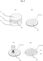
    shows several perspective views to illustrate exemplary steps (a), (b), (c), (d) for the fabrication of singulated chips from initial wafers,
    FIG. 10:
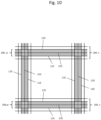
    shows a schematic view of pairs of outer weld lines defining dicing areas, wherein a single inner weld line extends within a dicing area,
    FIG. 11:
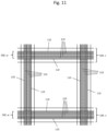
    shows a schematic view of pairs of outer weld lines defining dicing areas, wherein multiple inner weld line extend within a dicing area,
    FIG. 12:
    shows a sectional view of two welded substrates, wherein inner weld lines extend over both substrates,
    FIG. 13:
    shows a sectional view of two welded substrates, wherein inner weld lines extend within the volume of a single substrate,
    FIG. 14:
    shows a sectional view of two welded substrates, wherein the distance between inner weld lines is adjusted to the width of the dicing area,
    FIG. 15:
    shows a sectional view of a weld line,
    FIG. 16:
    shows an image of a first exemplary embodiment of welded substrates,
    FIG. 17:
    shows an image of a second exemplary embodiment of welded substrates,
    FIG. 18:
    shows two images (a), (b) of third exemplary embodiments of welded substrates.
  • FIG. 1 shows a first substrate 10 in the form of a wafer and a second substrate 20 in the form of a wafer, wherein the substrates 10, 20 are stacked on top of each other. By means of a laser 600, pairs of outer weld lines 110 are introduced into the first and second substrates 10, 20 such that the first and second substrates 10, 20 are welded together. Again, by means of a laser 600, inner weld lines 210 extending between a pair of outer weld lines 110 are introduced into at least one of the two substrates 10, 20. In areas closed all around by weld lines, functional areas 400 are defined.
  • These functional areas 400 can be singulated by dicing the welded substrates 10, 20 between the functional areas 400 within dicing areas 200 extending between outer weld lines 110. Dicing the welded substrates 10, 20 into multiple singulated chips 1 can be carried out by different cutting methods such as by means of a sawing blade, scribing and subsequent breaking, laser perforation and subsequent etching or subsequent breaking or the like. When cutting the welded substrates along a cutting trench, at least one of the inner weld lines 210 extending within the dicing area 200 may be seized by the cutting method.
  • FIGS. 2 and 3 show a singulated chip 1 manufactured by dicing the welded two wafers 10, 20. The singulated chip 1 comprises a first substrate 10, a second substrate 20 and a functional area 400 which is hermetically enclosed by surrounding weld lines 110, 310, one of which being a partial weld line 310 directly positioned at the lateral edge of the singulated chip 1.
  • FIG. 4 shows three wafers 10, 20, 30, wherein the lower two wafers 20, 30 are already an assembled wafer stack of two substrates being welded together. The upper wafer 10 is an individual wafer which is brought in contact with the outer wafer 20 of the lower wafer stack. By means of a laser 600, outer weld lines 110 are introduced into the upper individual wafer 10 and the outer wafer 20 of the lower wafer stack so as to weld together the two wafers 10, 20. Again, by means of a laser 600, inner weld lines 210 extending between a pair of outer weld lines 110 are introduced into at least one of the two substrates 10, 20.
  • FIGS. 5 to 8 show a singulated chip 1 manufactured by dicing the welded wafer stack 10, 20, 30. The singulated chip 1 comprises an upper first substrate 10, an intermediate second substrate 20 and a lower third substrate 30, wherein the intermediate second substrate 20 is a spacer substrate comprising a cavity 500 extending through the entire thickness of the spacer substrate. The cavity 500 may house a functional element 510, e.g. a microchip. The cavity 500 is hermetically sealed by surrounding weld lines 110, 310 bonding the first and second substrates 10, 20 as well as the second and third substrates 20, 30. At the lateral edge, the singulated chip 1 comprises several partial weld lines 310.
  • FIG. 9 shows several exemplary steps for the fabrication of singulated chips from initial wafers, in this case three wafers 10, 20, 30. In step (a) some or all of the wafers are aligned with respect to each other and/or with respect to components to be sealed. For example, spacer wafer 20 comprising cavities 500 may be aligned with respect to functional components attached on lower wafer 30 and upper wafer 10 may be aligned with respect to spacer wafer 20 and/or lower wafer 30. In step (b) the wafers 10, 20, 30 are brought into contact such that contact areas are defined between adjacent wafers, in this case between wafers 10, 20 and between wafers 20, 30. In step (c) adjacent wafers 10, 20 and 20, 30 are welded together by means of a laser 600, wherein weld lines are introduced in the contact area as described further above. In step (d) welded wafer stack 10, 20, 30 may be diced into multiple singulated chips, wherein dicing may be carried out along dicing trenches 250 extending along the contact areas comprising the weld lines.
  • FIGS. 10 and 11 show contact areas 100 between two substrates and pairs of outer weld lines 110 introduced within these contact areas 100, wherein the outer weld lines 110 are the outermost weld lines 110 adjacent to the two edges of the contact area 100. The contact area has a width v. In between these outer weld lines 110 a dicing area 200 is defined which is intended for cutting and dicing the welded substrates, preferably without impairing the outer weld lines 110. The dicing area has a width w, wherein w<=v, preferably w<v. Within the dicing area 200, one or more inner weld lines 210 is introduced, for example one inner weld lines 210 (FIG. 10) or four inner weld lines 210 (FIG. 11). An advantage of less weld lines may be a shorter production time. Preferably, cutting the welded substrates is carried out on one or more inner weld lines 210, so that partial weld lines 310 remain at the edges of the singulated chips 1.
  • FIG. 12 shows an embodiment of two welded substrates 10, 20, wherein two outer weld lines 110 are introduced on each side of the dicing area 200 and multiple inner weld lines 210 are introduced within the dicing area 200. In this case, inner weld lines 210 are positioned at equal distances and at equal focal positions, i.e., at equal depths within the substrates, relative to the outer weld lines 110. In this case, both the outer weld lines 110 and the inner weld lines 210 are positioned at the interface of the two substrates 10, 20 and thus weld together the two substrates 10, 20.
  • FIG. 13 shows an embodiment of two welded substrates 10, 20, wherein a single outer weld line 110 is introduced on each side of the dicing area 200 and multiple inner weld lines 210 are introduced within the dicing area 200. In this case, inner weld lines 210 have a greater distance to the outer weld lines 110 than inner weld lines 210 have with respect to each other. Furthermore, inner weld lines are positioned within the volume of one of the substrates, in this case the lower substrate 20. Thus, inner weld lines are not contributing to welding together the two substrates 10, 20. An advantage may be that material in the separation zone is easier to separate from singulated chips, since it falls apart.
  • FIG. 14 shows an embodiment of two welded substrates 10, 20, with outer weld lines 110 and inner weld lines 210 introduced in the two substrates. The inner weld lines preferably are introduced such that the fraction d/w is smaller than 3, preferably smaller than 2, wherein d is the distance between adjacent inner weld lines 210 and w is the width of the dicing area 200. As described above, at least one or some of the inner weld lines may be in the plane of the outer weld lines and/or may be entirely in the volume of one of the substrates.
  • FIG 15 shows a weld line, wherein the weld line comprises several regions or areas such an area of nonlinear absorption 350, an elongated bubble 360, preferably starting from the area of nonlinear absorption, a melting region 370, preferably surrounding the elongated bubble, and/or a heating region 380, preferably surrounding the elongated bubble and/or the melting region.
  • FIG 16 shows an image of a first exemplary embodiment of welded substrates defining functional areas 400 and/or cavities 500 between contact areas 100 and comprising several weld lines forming an orthogonal grid. In this case, the weld line pitch is in a range of 20 µm to 60 pm, for example 40 µm. The width of the weld zone is between 250 µm and 450 pm, for example 360 µm.
  • FIG 17 shows an image of a second exemplary embodiment of welded substrates defining functional areas 400 and/or cavities 500 between contact areas 100 and comprising several weld lines forming an orthogonal grid. In this case, the weld line pitch is in a range of 20 µm to 200 pm, for example 100 µm. The width of the weld zone is between 50 µm and 5000 pm, for example 3000 µm. The width of a dicing trench 250 is between 150 µm and 450 pm, for example 310 µm.
  • FIG 18 shows embodiments of a singulated glass enclosure 1. It has been cut in half and polished at the cutting side in order to show the weld lines in the microscope pictures. It is comprised of three substrates 10, 20, 30 welded together by weld lines 110, 210, 310. The substrates, in this case, are made of Borofloat33 glass with thicknesses of 320 pm, 500 µm and 320 µm respectively, that enclose a cavity 500. In this case, as in FIG 16, the weld line pitch is in a range of 20 µm to 60 pm, for example 40 µm. The width of the weld zone is between 250 µm and 450 pm, for example 360 µm. The singulation has been done with a dicing saw.
  • List of reference signs
  • 1
    Singulated chip
    10
    First substrate
    20
    Second substrate
    30
    Third substrate
    100
    Contact area of width v
    110
    Outer weld line
    200
    Dicing area of width w
    210
    Inner weld line
    250
    Dicing trench
    310
    Partial weld line
    350
    Area of nonlinear absorption
    360
    Elongated bubble
    370
    Melting region
    380
    Heating region
    400
    Functional area
    500
    Cavity
    510
    Functional element
    600
    Laser

Claims (19)

  1. Method for welding substrates comprising:
    Bringing a first substrate (10) and a second substrate (20) in contact with each other such that a contact area (100) between the two substrates is formed,
    Introducing at least two outer weld lines (110) extending next to each other within the contact area (100) into the first and second substrates (10, 20) such that the first and second substrates (10, 20) are welded together by each of the outer weld lines (110) and such that a dicing area (200) is defined between the two outer weld lines (110),
    Introducing one or more inner weld lines (210) extending between the two outer weld lines (110) within the dicing area into at least one of the two substrates.
  2. Method according to the preceding claim,
    wherein the first substrate is an integrally formed individual substrate,
    wherein the second substrate is an integrally formed individual substrate or an outer substrate of an assembled substrate stack comprising one or more substrates.
  3. Method according to any one of the preceding claims, further comprising:
    Dicing the welded substrates into multiple singulated chips by cutting the welded substrates within the dicing area,
    wherein preferably the cutting is performed on at least one of the inner weld lines extending within the dicing area.
  4. Method according to any one of the preceding claims, in particular according to claim 1 or 2,
    wherein the cutting of the welded substrates is carried out by means of a sawing blade,
    wherein preferably the sawing blade seizes at least one of the inner weld lines extending within the dicing area.
  5. Method according to any one of the preceding claims, in particular according to claim 1 or 2,
    wherein the cutting of the welded substrates is carried out by scribing and subsequent breaking.
  6. Method according to any one of the preceding claims, in particular according to claim 1 or 2,
    wherein the cutting of the welded substrates is carried out by laser perforation in which adjacent perforations are introduced into the substrates and subsequent etching in which an etching fluid is used to connect the adjacent perforations and/or by subsequent application of stress, e.g. mechanical stress and/or thermal stress.
  7. Method according to any one of the preceding claims,
    wherein the cross-section of an outer and/or inner weld line is characterized by at least one of the following features:
    an area of nonlinear absorption (350),
    an elongated bubble (360), preferably starting from the area of nonlinear absorption,
    a melting region (370), preferably surrounding the elongated bubble,
    a heating region (380), preferably surrounding the elongated bubble and/or the melting region.
  8. Method according to any one of the preceding claims,
    wherein the contact area has a width of less than 5 mm, preferably of less than 2 mm, more preferably of less than 1 mm most preferably less than 0.6 mm and/or
    wherein the contact area has a width of more than 0.1 mm, preferably of more than 0.4, more preferably of more than 0.6 mm.
  9. Method according to any one of the preceding claims,
    wherein the dicing area has a width of less than 2 mm, preferably of less than 1 mm, more preferably of less than 0.3 mm and/or
    wherein the dicing area has a width of more than 0.05 mm, preferably of more than 0.1 mm, more preferably of more than 0.2 mm.
  10. Method according to any one of the preceding claims,
    wherein at least 2 inner weld lines are introduced, preferably at least 4 inner weld lines are introduced, more preferably at least 8 inner weld lines are introduced, and/or
    wherein two adjacent inner weld lines have a distance d to each other which is smaller than 0.3 mm, preferably smaller than 0.15 mm, more preferably smaller than 0.05 mm, and/or
    wherein the inner weld lines are introduced such that the fraction d/w is smaller than 3, preferably smaller than 2, wherein d is the distance between adjacent inner weld lines and w is the width of the dicing area.
  11. Method according to any one of the preceding claims, further comprising:
    defining a minimum shear force Fmin that the welding of the first and second substrates needs to withstand, and
    introducing a number of outer and/or inner weld lines such as to achieve the defined minimum shear force Fmin.
  12. Method according to any one of the preceding claims,
    wherein at least 2 outer weld line is introduced on each side of the dicing area, preferably at least 3 outer weld lines are introduced on each side of the dicing area, more preferably at least 4 outer weld lines are introduced on each side of the dicing area, and/or
    wherein two adjacent outer weld lines have a distance d to each other which is smaller than 0.3 mm, preferably smaller than 0.15 mm, more preferably smaller than 0.05 mm.
  13. Method according to any one of the preceding claims,
    wherein the first substrate, in particular the individual substrate, comprises one of the following materials: glass, glass ceramic, borosilicate glass, crystal, sapphire, diamond and/or
    wherein the second substrate comprises one of the following materials: glass, glass ceramic, borosilicate glass, crystal, sapphire, diamond, silicon, metal.
  14. Method according to any one of the preceding claims,
    wherein the first and/or second substrate has a thickness in the range of 0.03 mm to 20 mm, preferably in the range of 0.1 mm to 4 mm, more preferably in the range of 0.2 mm to 2 mm and/or
    wherein the first and/or second substrate have a lateral dimension in the range of 30 mm to 1000 mm, preferably in the range of 50 mm to 500 mm.
  15. Method according to any one of the preceding claims,
    wherein a plurality of dicing areas are introduced into the two substrates,
    wherein preferably the plurality of dicing areas defines a grid.
  16. Welded substrates comprising:
    at least a first substrate (10) and a second substrate (20),
    wherein the first and second substrates (10, 20) are in contact with each other such that a contact area (100) between the two substrates is formed,
    at least two outer weld lines (110) extending next to each other within the contact area (100) within the first and second substrates (10, 20) such that the first and second substrates (10, 20) are welded together by each of the outer weld lines and such that a dicing area (200) is defined between the two outer weld lines,
    one or more inner weld lines (210) extending
    between the two outer weld lines (110) within the dicing area (200) within at least one of the two substrates (10, 20),
    wherein preferably one or more functional areas (400) are defined which each are hermetically enclosed by the dicing areas.
  17. Welded substrates according to the preceding claim further comprising:
    a third substrate (30),
    wherein the second and third substrates (20, 30) are in contact with each other such that a contact area (200) between the two substrates is formed,
    at least two outer weld lines (110) extending next to each other within the contact area (200) within the second and third substrates (20, 30) such that the second and third substrates (20, 30) are welded together by each of the outer weld lines and such that a dicing area (200) is defined between the two outer weld lines,
    one or more inner weld lines (210) extending
    between the two outer weld lines (110) within the dicing area 200) within at least one of the two substrates (20, 30),
    wherein preferably one or more cavities (500) are defined which each are hermetically enclosed by the dicing areas.
  18. Singulated chip (1), in particular hermetically sealed enclosure, comprising
    at least a first substrate (10) and a second substrate (20),
    wherein the first and second substrates (10, 20) are in contact with each other and are welded together by weld lines,
    wherein a functional area (400) is defined which is hermetically enclosed by weld lines, and wherein at least one weld line or a partial weld line (310) is positioned at the lateral edge of at least one substrate.
  19. Singulated chip (1) according to the preceding claim further comprising:
    a third substrate (30),
    wherein the second and third substrates (20, 30) are in contact with each other and are welded together by weld lines,
    wherein a cavity (500) is defined which is hermetically enclosed by weld lines, and wherein at least one weld line or a partial weld line (310) is positioned at the lateral edge of at least one substrate.
EP22216975.7A 2022-12-28 2022-12-28 Method for welding substrates and welded substrates Pending EP4393869A1 (en)

Priority Applications (5)

Application Number Priority Date Filing Date Title
EP22216975.7A EP4393869A1 (en) 2022-12-28 2022-12-28 Method for welding substrates and welded substrates
PCT/EP2023/086263 WO2024141298A1 (en) 2022-12-28 2023-12-18 Method for welding substrates and welded substrates
JP2025538350A JP2026501017A (en) 2022-12-28 2023-12-18 Substrate welding method and welded substrate
CN202380089961.1A CN120390721A (en) 2022-12-28 2023-12-18 Method for welding substrate and welded substrate
AU2023414425A AU2023414425A1 (en) 2022-12-28 2023-12-18 Method for welding substrates and welded substrates

Applications Claiming Priority (1)

Application Number Priority Date Filing Date Title
EP22216975.7A EP4393869A1 (en) 2022-12-28 2022-12-28 Method for welding substrates and welded substrates

Publications (1)

Publication Number Publication Date
EP4393869A1 true EP4393869A1 (en) 2024-07-03

Family

ID=84688320

Family Applications (1)

Application Number Title Priority Date Filing Date
EP22216975.7A Pending EP4393869A1 (en) 2022-12-28 2022-12-28 Method for welding substrates and welded substrates

Country Status (5)

Country Link
EP (1) EP4393869A1 (en)
JP (1) JP2026501017A (en)
CN (1) CN120390721A (en)
AU (1) AU2023414425A1 (en)
WO (1) WO2024141298A1 (en)

Citations (4)

* Cited by examiner, † Cited by third party
Publication number Priority date Publication date Assignee Title
US20170279247A1 (en) * 2014-08-25 2017-09-28 Corning Incorporated Sealed device and methods for making the same
EP3012059B1 (en) * 2014-09-26 2017-10-18 Primoceler Oy Method to produce a transparent piece to be used to protect an optical component
US20220219972A1 (en) * 2019-09-26 2022-07-14 Schott Ag Hermetically sealed glass package
US20220241897A1 (en) * 2019-10-24 2022-08-04 Schott Primoceler Oy Glass compound arrangement

Patent Citations (4)

* Cited by examiner, † Cited by third party
Publication number Priority date Publication date Assignee Title
US20170279247A1 (en) * 2014-08-25 2017-09-28 Corning Incorporated Sealed device and methods for making the same
EP3012059B1 (en) * 2014-09-26 2017-10-18 Primoceler Oy Method to produce a transparent piece to be used to protect an optical component
US20220219972A1 (en) * 2019-09-26 2022-07-14 Schott Ag Hermetically sealed glass package
US20220241897A1 (en) * 2019-10-24 2022-08-04 Schott Primoceler Oy Glass compound arrangement

Also Published As

Publication number Publication date
JP2026501017A (en) 2026-01-13
AU2023414425A1 (en) 2025-06-05
WO2024141298A1 (en) 2024-07-04
CN120390721A (en) 2025-07-29

Similar Documents

Publication Publication Date Title
US7808059B2 (en) Semiconductor substrate, and semiconductor device and method of manufacturing the semiconductor device
CN102903745B (en) Semiconductor device and manufacture method thereof
US8609512B2 (en) Method for laser singulation of chip scale packages on glass substrates
TW559876B (en) Method and apparatus for dicing a semiconductor wafer
US8148240B2 (en) Method of manufacturing semiconductor chips
JP2005167190A (en) Semiconductor wafer dicing method
US8212180B2 (en) Method for severing brittle flat materials by laser beam with previously produced traces
CN108682648B (en) Method for cutting wafer and semiconductor chip
US6777311B2 (en) Thick wafer processing and resultant products
CN108231658A (en) Substrate processing method using same
KR20160026860A (en) Semiconductor piece manufacturing method, circuit board including semiconductor piece, and image forming apparatus
US20080233714A1 (en) Method for fabricating semiconductor device
US8030180B2 (en) Method of manufacturing a semiconductor device
JP2010232378A (en) Manufacturing method of semiconductor device
WO2007005823A2 (en) Semiconductor wafer cutting blade and method
JP2012186309A (en) Manufacturing method of wafer level package, and wafer level package
JP5127669B2 (en) Semiconductor wafer
JP2007165371A (en) Manufacturing method of semiconductor device
EP4393869A1 (en) Method for welding substrates and welded substrates
CN115871116A (en) Slicing of silicon carbide semiconductor wafers
US7179720B2 (en) Pre-fabrication scribing
JPH1070094A (en) Semiconductor sensor wafer cutting method
JPH04251960A (en) Manufacture of semiconductor wafer and semiconductor device
KR20240177934A (en) Semiconductor device and method for manufacturing the same
CN121728991A (en) Method for manufacturing semiconductor device and semiconductor device

Legal Events

Date Code Title Description
STAA Information on the status of an ep patent application or granted ep patent

Free format text: STATUS: EXAMINATION IS IN PROGRESS

PUAI Public reference made under article 153(3) epc to a published international application that has entered the european phase

Free format text: ORIGINAL CODE: 0009012

17P Request for examination filed

Effective date: 20221228

AK Designated contracting states

Kind code of ref document: A1

Designated state(s): AL AT BE BG CH CY CZ DE DK EE ES FI FR GB GR HR HU IE IS IT LI LT LU LV MC ME MK MT NL NO PL PT RO RS SE SI SK SM TR

RBV Designated contracting states (corrected)

Designated state(s): AL AT BE BG CH CY CZ DE DK EE ES FI FR GB GR HR HU IE IS IT LI LT LU LV MC ME MK MT NL NO PL PT RO RS SE SI SK SM TR

P01 Opt-out of the competence of the unified patent court (upc) registered

Free format text: CASE NUMBER: APP_56266/2024

Effective date: 20241015