EP4391385A1 - Direct digital synthesizer module, measurement system, and method of operating a direct digital synthesizer module - Google Patents
Direct digital synthesizer module, measurement system, and method of operating a direct digital synthesizer module Download PDFInfo
- Publication number
- EP4391385A1 EP4391385A1 EP22216129.1A EP22216129A EP4391385A1 EP 4391385 A1 EP4391385 A1 EP 4391385A1 EP 22216129 A EP22216129 A EP 22216129A EP 4391385 A1 EP4391385 A1 EP 4391385A1
- Authority
- EP
- European Patent Office
- Prior art keywords
- module
- phase
- signal
- sub
- dds
- Prior art date
- Legal status (The legal status is an assumption and is not a legal conclusion. Google has not performed a legal analysis and makes no representation as to the accuracy of the status listed.)
- Pending
Links
Images


Classifications
-
- H—ELECTRICITY
- H03—ELECTRONIC CIRCUITRY
- H03L—AUTOMATIC CONTROL, STARTING, SYNCHRONISATION OR STABILISATION OF GENERATORS OF ELECTRONIC OSCILLATIONS OR PULSES
- H03L7/00—Automatic control of frequency or phase; Synchronisation
- H03L7/06—Automatic control of frequency or phase; Synchronisation using a reference signal applied to a frequency- or phase-locked loop
- H03L7/08—Details of the phase-locked loop
- H03L7/099—Details of the phase-locked loop concerning mainly the controlled oscillator of the loop
- H03L7/0991—Details of the phase-locked loop concerning mainly the controlled oscillator of the loop the oscillator being a digital oscillator, e.g. composed of a fixed oscillator followed by a variable frequency divider
- H03L7/0994—Details of the phase-locked loop concerning mainly the controlled oscillator of the loop the oscillator being a digital oscillator, e.g. composed of a fixed oscillator followed by a variable frequency divider comprising an accumulator
-
- G—PHYSICS
- G06—COMPUTING OR CALCULATING; COUNTING
- G06F—ELECTRIC DIGITAL DATA PROCESSING
- G06F1/00—Details not covered by groups G06F3/00 - G06F13/00 and G06F21/00
- G06F1/02—Digital function generators
- G06F1/03—Digital function generators working, at least partly, by table look-up
- G06F1/0321—Waveform generators, i.e. devices for generating periodical functions of time, e.g. direct digital synthesizers
- G06F1/0328—Waveform generators, i.e. devices for generating periodical functions of time, e.g. direct digital synthesizers in which the phase increment is adjustable, e.g. by using an adder-accumulator
-
- G—PHYSICS
- G01—MEASURING; TESTING
- G01R—MEASURING ELECTRIC VARIABLES; MEASURING MAGNETIC VARIABLES
- G01R31/00—Arrangements for testing electric properties; Arrangements for locating electric faults; Arrangements for electrical testing characterised by what is being tested not provided for elsewhere
- G01R31/28—Testing of electronic circuits, e.g. by signal tracer
- G01R31/2832—Specific tests of electronic circuits not provided for elsewhere
- G01R31/2836—Fault-finding or characterising
- G01R31/2839—Fault-finding or characterising using signal generators, power supplies or circuit analysers
- G01R31/2841—Signal generators
-
- G—PHYSICS
- G06—COMPUTING OR CALCULATING; COUNTING
- G06F—ELECTRIC DIGITAL DATA PROCESSING
- G06F1/00—Details not covered by groups G06F3/00 - G06F13/00 and G06F21/00
- G06F1/02—Digital function generators
- G06F1/022—Waveform generators, i.e. devices for generating periodical functions of time, e.g. direct digital synthesizers
-
- G—PHYSICS
- G06—COMPUTING OR CALCULATING; COUNTING
- G06F—ELECTRIC DIGITAL DATA PROCESSING
- G06F1/00—Details not covered by groups G06F3/00 - G06F13/00 and G06F21/00
- G06F1/02—Digital function generators
- G06F1/03—Digital function generators working, at least partly, by table look-up
- G06F1/0321—Waveform generators, i.e. devices for generating periodical functions of time, e.g. direct digital synthesizers
- G06F1/0328—Waveform generators, i.e. devices for generating periodical functions of time, e.g. direct digital synthesizers in which the phase increment is adjustable, e.g. by using an adder-accumulator
- G06F1/0335—Waveform generators, i.e. devices for generating periodical functions of time, e.g. direct digital synthesizers in which the phase increment is adjustable, e.g. by using an adder-accumulator the phase increment itself being a composed function of two or more variables, e.g. frequency and phase
-
- G—PHYSICS
- G06—COMPUTING OR CALCULATING; COUNTING
- G06F—ELECTRIC DIGITAL DATA PROCESSING
- G06F1/00—Details not covered by groups G06F3/00 - G06F13/00 and G06F21/00
- G06F1/04—Generating or distributing clock signals or signals derived directly therefrom
- G06F1/08—Clock generators with changeable or programmable clock frequency
Definitions
- the invention generally relates to a direct digital synthesizer module.
- the invention further relates to a measurement system and to a method of operating a direct digital synthesizer module.
- Direct digital synthesizers are, referred to the CLK of the phase accumulator, highly phase stable. Modern direct digital synthesizers enable the user to set the frequency and initial phase via dedicated registers, namely via an FTW (frequency tuning word) and an initial phase.
- FTW frequency tuning word
- phase relation is usually achieved by setting the respective initial phase values of the direct digital synthesizers, wherein the initial phase values of all direct digital synthesizers have to be set simultaneously within a single clock cycle.
- the object of the present invention is to provide a direct signal synthesizer module that allows for a less time-critical setting of the phase relation.
- the DDS module comprises a phase accumulator module.
- the phase accumulator module comprises a clock input being configured to receive a clock signal.
- the phase accumulator module further comprises a frequency tuning register being configured to receive a frequency tuning word (FTW).
- the phase accumulator module further comprises a phase shift register being configured to receive a phase shift word (PSW).
- the phase accumulator module further comprises a phase increment sub-module being configured to increment a phase signal output by the phase accumulator module by a predetermined phase increment based on the clock signal and/or based on the FTW.
- the phase accumulator module further comprises a feedback path being configured to feed back the phase signal to the phase increment sub-module.
- the phase accumulator module further comprises a phase correction sub-module, wherein the phase correction sub-module is configured to adapt the phase signal fed back to the phase increment sub-module based on the phase shift word.
- module is understood to describe suitable hardware, suitable software, or a combination of hardware and software that is configured to have a certain functionality.
- the hardware may, inter alia, comprise a CPU, a GPU, an FPGA, an ASIC, or other types of electronic circuitry.
- the phase signal fed back to the phase increment sub-module is adapted based on the PSW in order to obtain a desired phase signal that is output by the phase accumulator module.
- phase of an output signal of the DDS module is adapted by adapting the phase signal fed back to the phase increment sub-module based on the PSW.
- a desired phase relation between an output signal of the DDS module and another signal can be obtained by providing the PSW to the DDS module.
- phase signal fed back to the phase increment sub-module can be adapted in an arbitrary clock cycle of the phase accumulator module.
- phase correction is applied to the phase signal fed back to the phase increment sub-module, which is not time-critical and does not require a precise coordination of multiple different DDS modules.
- the DDS module may comprise a converter module downstream of the phase accumulator module, wherein the converter module is configured to convert the phase signal output by the phase accumulator module into an amplitude signal.
- the converter module is configured to map the phase of the phase signal to a corresponding amplitude of the amplitude signal, such that signals having arbitrary shape can be generated, e.g. sine-shaped amplitude signals, sawtooth-shaped amplitude signals, etc.
- the DDS module may comprises a digital-to-analog converter (DAC) downstream of the phase accumulator module, particularly downstream of the converter module.
- the DAC is configured to convert a digital output signal of the DDS module, particularly the amplitude signal, into an analog output signal of the DDS module.
- the DDS module may be integrated on a chip.
- the chip may be a dedicated DDS chip.
- the DDS module may also be integrated on a chip together with other electronic components.
- the phase correction sub-module is configured to receive a phase shift trigger signal, wherein the phase correction sub-module is configured to adapt the phase signal fed back to the phase increment sub-module upon receiving the phase shift trigger signal.
- the timing of adapting the phase signal fed back to the phase increment sub-module can be controlled by providing the phase shift trigger signal to the phase correction sub-module.
- the phase correction sub-module is configured to replace the phase signal fed back to the phase increment sub-module with a corrected phase signal.
- the phase correction sub-module comprises a multiplexer sub-module, wherein the multiplexer sub-module is configured to selectively forward the phase signal or the corrected phase signal to the phase increment sub-module. In other words, instead of feeding back an actual phase signal output by the phase increment sub-module, the corrected phase signal is fed back or rather forwarded to the phase increment sub-module. This way, an arbitrary phase signal can be set.
- the corrected phase signal may correspond to the desired phase signal that should be output by the phase accumulator module in the current clock cycle.
- the multiplexer sub-module may be configured or rather controlled to feed back the phase signal output by the phase increment sub-module to the phase increment sub-module.
- the multiplexer sub-module is controlled to forward the corrected phase signal to the phase increment sub-module instead of the actual phase signal output by the phase increment sub-module for a predetermined time interval, e.g. for one clock cycle.
- the multiplexer sub-module may be controlled by means of the phase shift trigger signal described above, such that the multiplexer sub-module forwards the corrected phase signal to the phase increment sub-module upon receiving the phase shift trigger signal.
- the phase correction sub-module is configured to replace the phase signal fed back to the phase increment sub-module with a corrected phase signal during a single clock cycle of the clock signal. Accordingly, during a certain clock cycle, the phase correction sub-module receives the corrected phase signal instead of the phase signal output by the phase correction sub-module. During the next clock cycle, the phase correction sub-module receives the phase signal output by the phase correction sub-module via the feedback path, which corresponds to the corrected phase signal incremented by the predetermined phase increment.
- the correction or rather adaptation of the phase of the output signal of the DDS module can be performed within a single clock cycle.
- phase correction sub-module is configured to add a phase correction signal to the phase signal fed back to the phase increment sub-module.
- the phase correction sub-module comprises an adder sub-module, wherein the adder sub-module is configured to add the phase correction signal to the phase signal fed back to the phase increment sub-module.
- the phase signal output by the phase increment sub-module is corrected by adding the phase correction signal, such that a desired phase signal is obtained.
- the phase correction signal may correspond to the difference between the desired phase signal and the actual phase signal output by the phase accumulator module in the current clock cycle.
- the phase correction sub-module may comprise a multiplexer sub-module, wherein the multiplexer sub-module is configured to selectively forward the phase correction signal to the adder sub-module. More precisely, the multiplexer sub-module is configured to selectively forward the phase correction signal or a zero-signal to the adder sub-module, wherein the zero-signal does not alter the phase signal when added to the phase signal.
- the multiplexer sub-module may be configured or rather controlled to forward the zero-signal to the adder sub-module or to forward no signal at all.
- the multiplexer sub-module is controlled to forward the phase correction signal to the adder sub-module for a predetermined time interval, e.g. for one clock cycle.
- the multiplexer sub-module may be controlled by means of the phase shift trigger signal described above, such that the multiplexer sub-module forwards the phase correction signal to the adder sub-module upon receiving the phase shift trigger signal.
- the phase correction sub-module is configured to add the phase correction signal to the phase signal fed back to the phase increment sub-module during a single clock cycle of the clock signal.
- the correction or rather adaptation of the phase of the output signal of the DDS module can be performed within a single clock cycle.
- the problem further is solved by a measurement system.
- the measurement system comprises at least one DDS module described above.
- the measurement system may comprise a measurement instrument, wherein the at least one DDS module is integrated into the measurement instrument.
- the measurement instrument may be an oscilloscope, particularly a digital oscilloscope, a vector network analyzer, a spectrum analyzer, a standalone signal generator, etc.
- the measurement system comprises an analysis module, wherein the analysis module is configured to receive an analog output signal of the at least one DDS module, wherein the analysis module is further configured to receive a phase reference signal, and wherein the analysis module is configured to determine the PSW based on the analog output signal of the at least one DDS module and based on the phase reference signal.
- the analysis module may be configured to determine a phase difference between the analog output signal of the at least one DDS module and the phase reference signal.
- the analysis module may further be configured to determine the PSW based on the determined phase difference.
- the analysis module may further be configured to forward the determined PSW to the at least one DDS module, or more precisely to the phase shift register of the at least one DDS module.
- the analysis module may be integrated into the measurement instrument described above.
- the analysis module is integrated into another electronic device.
- the measurement system comprises at least one further DDS module, wherein the phase reference signal is an analog output signal of the at least one further DDS module.
- the at least one further DDS module may be configured like the DDS module described above, but this is not necessary.
- N-1) PSWs have to be determined by means of the analysis module.
- the phases of the analog output signals of (N-1) DDS modules may be adapted relative to the phase of the analog output signal of the remaining DDS module based on the (N-1) determined PSWs.
- the analysis module is configured to repeatedly determine the PSW in predefined time intervals.
- the phase relation between the analog output signal of the at least one DDS module and the phase reference signal may be monitored continuously, and the phase of the analog output signal of the at least one DDS module may be corrected by providing an appropriate PSW to the at least one DDS module if necessary.
- the analysis module may be configured to determine the PSW after the FTW of the at least one DDS module has been updated. Thus, it is ensured that a desired phase relation between the analog output signal of the at least one DDS module and the phase reference signal is obtained after the FTW has been updated.
- the measurement system comprises a directional coupler, wherein the directional coupler is configured to forward the analog output signal of the at least one DDS module to the analysis module.
- the directional coupler may further be configured to forward the analog output signal of the at least one DDS module to a measurement port, to another electronic component, or to another signal path.
- the directional coupler is established as a 3-port coupler.
- the measurement system may comprise at least one further directional coupler, wherein the at least one further directional coupler is configured to forward the phase reference signal the analysis module.
- the at least one further directional coupler may further be configured to forward the phase reference signal to a measurement port, to another electronic component, or to another signal path.
- the at least one further directional coupler is established as a 3-port coupler.
- the measurement system may comprise at least one further DDS module, wherein the measurement system comprises a common clock source for the at least one DDS module and for the at least one further DDS module.
- the problem further is solved by a method of operating a direct digital synthesizer (DDS) module, wherein the DDS module is established as described above.
- the method comprises the steps of:
- the phrase "at least one of A, B, and C", for example, means (A), (B), (C), (A and B), (A and C), (B and C), or (A, B, and C), including all further possible permutations when more than three elements are listed.
- the term “at least one of A and B” generally means “A and/or B", namely "A” alone, “B” alone or "A and B”.
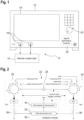
- Figure 1 schematically shows a measurement system 10 comprising a measurement instrument 12 and a device under test 14.
- the measurement instrument 12 may be established as any type of measurement instrument being suitable to perform measurements on the electronic device under test 14.
- the measurement instrument 12 may be established as an oscilloscope, particularly as a digital oscilloscope, as a vector network analyzer, as a spectrum analyzer, as a signal generator, etc.
- the measurement instrument 12 comprises two measurement ports 16, wherein measurements can be conducted on the device under test 14 via the measurement ports 16.
- signals can be received from the device under test 14 and/or forwarded to the device under test 14 via the measurement ports 16 in order to perform the measurements on the device under test 14.
- the measurement instrument 12 may comprise an arbitrary number of measurement ports 16 other than two.
- the measurement instrument 12 may further comprise a display 18 and/or control means 20, wherein settings of the measurement instrument 12 may be adaptable by a user via the control means 20.
- the measurement instrument 12 further comprises a signal generator module 22 that is shown in more detail in Figure 2 .
- the signal generator module 22 comprises a first direct digital synthesizer (DDS) module 24 and a second DDS module 26.
- DDS direct digital synthesizer
- the first DDS module 24 and the second DDS module 26 are configured to generate an analog output signal, respectively.
- the signal generator module 22 is configured to generate two analog outputs signals that may be employed in order to conduct measurements on the device under test 14.
- the measurement system 10, particularly the signal generator module 22, may comprise an arbitrary number of DDS modules.
- the analog output signals may be used as reference signals for conducting the measurements.
- the analog output signals may be forwarded to different ports of the device under test 14, particularly wherein the analog output signals may correspond to a differential signal.
- the analog output signals may be processed by the device under test 14 and/or partially reflected at input ports of the device under test 14, and the corresponding processed and/or reflected signals may be measured by means of the measurement instrument 12.
- the signal generator module 22 further comprises a clock source 28 that is configured to provide a clock signal to the first DDS module 24 and to the second DDS module 26.
- the signal generator module 22 comprises a dedicated clock source for each DDS module 24, 26.
- the signal generator module 22 further comprises an analysis module 30 that comprises a phase determination unit 32 and a phase adjustment processing unit 34, the functionality of which will be described in more detail below.
- the signal generator module 22 further comprises a first directional coupler 36 that is configured to forward the analog output signal of the first DDS module 24 to the analysis module 30.
- the first directional coupler 36 is further configured to forward the analog output signal of the first DDS module 24 to one of the measurement ports 16 or to another electronic component of the measurement instrument 12.
- the first directional coupler 36 is established as a 3-port coupler.
- the signal generator module 22 further comprises a second directional coupler 38 that is configured to forward the analog output signal of the second DDS module 26 to the analysis module 30.
- the second directional coupler 38 is further configured to forward the analog output signal of the second DDS module 26 to one of the measurement ports 16 or to another electronic component of the measurement instrument 12.
- the second directional coupler 38 is established as a 3-port coupler.
- the signal generator module 22 further comprises a control- and trigger module 39, the functionality of which will be described in more detail below.
- Figure 3 schematically shows a first variant of the first DDS module 24.
- the first DDS module 24 may be integrated on a dedicated DDS chip.
- the first DDS module 24 may be integrated on a chip together with other electronic components of the measurement instrument 12.
- the DDS module 24 comprises a phase accumulator module 40.
- the phase accumulator module 40 comprises a clock input 42 that is configured to receive a clock signal having a predefined frequency, namely the clock signal generated by the clock source 28.
- the phase accumulator module 40 further comprises a frequency tuning register 44 that is configured to receive and save a frequency tuning word (FTW), particularly from the control- and trigger module 39.
- FW frequency tuning word
- the FTW determines a frequency of an output signal of the DDS module 24 in relation to the frequency of the clock signal, as is well-known in the state of the art related to direct digital synthesizers.
- the phase accumulator module 40 further comprises an initial phase register 46 being configured to receive and save an initial phase for the phase accumulator module 40.
- frequency tuning register 44 and the initial phase register 46 may also be integrated into a single register.
- the phase accumulator module 40 further comprises a phase shift register 48 being configured to receive and save a phase shift word (PSW), particularly from the control- and trigger module 39 and/or from the analysis module 30.
- PSW phase shift word
- phase accumulator module 40 comprises an FTW trigger input 50 and a phase shift trigger input 52.
- the FTW trigger input 50 is configured to receive an FTW trigger signal, particularly from the control- and trigger module 39.
- the phase shift trigger input 52 is configured to receive a phase shift trigger signal, particularly from the control- and trigger module 39.
- the phase accumulator module 40 further comprises a phase increment sub-module 54 and a feedback path 56.
- the phase increment sub-module 54 is configured to increment a phase signal output by the phase accumulator module 40 by a predetermined phase increment based on the clock signal and/or based on the FTW.
- the feedback path 56 is configured to feed back the phase signal to the phase increment sub-module 54.
- the phase accumulator module 40 further comprises a phase correction sub-module 58.
- the phase correction sub-module 58 is configured to adapt the phase signal fed back to the phase increment sub-module 54 based on the PSW, as will be described in more detail below.
- the first DDS module 24 further comprises a converter module 60 and a digital-to-analog converter (DAC) 62.
- DAC digital-to-analog converter
- the converter module 60 is provided downstream of the phase accumulator module 40, and is configured to convert the phase signal output by the phase accumulator module 40 into an amplitude signal.
- the converter module 60 is configured to map the phase of the phase signal to a corresponding amplitude of the amplitude signal, such that signals having arbitrary shape can be generated, e.g. sine-shaped amplitude signals, sawtooth-shaped amplitude signals, etc.
- the second DDS module 26 may be established identically to the first DDS module 24 described above and hereinafter.
- the second DDS module 26 may be established without the phase shift register 48, the phase shift trigger input 52, and the phase correction sub-module 58.
- Figure 4 shows a first variant of the first DDS module 24 described above or rather of the phase correction sub-module 58 of the first DDS module 24 described above.
- the phase correction sub-module 58 comprises a multiplexer sub-module 64 that is connected with the phase increment sub-module 54 via the feedback path 56.
- the multiplexer sub-module 64 is connected with the phase shift register 48 and with the phase shift trigger input 52.
- the multiplexer sub-module 64 is configured to selectively forward the phase signal output by the phase increment sub-module 54 or a corrected phase signal to the phase increment sub-module 54.
- the PSW saved in the phase shift register 48 corresponds to the corrected phase signal, i.e. a desired phase signal that should be output by the phase accumulator module 40 in the current clock cycle.
- the multiplexer sub-module 64 is controlled by the control- and trigger module 39 to feed back the phase signal output by the phase increment sub-module 54 to the phase increment sub-module 54.
- the multiplexer sub-module 64 is controlled by the control- and trigger module 39 to forward the corrected phase signal saved in the phase shift register 48 to the phase increment sub-module 54 for exactly one clock cycle of the clock signal.
- phase signal output by the phase increment sub-module 54 is replaced by the corrected phase signal for one clock cycle.
- control- and trigger module 39 generates a phase shift trigger signal that is forwarded to the multiplexer sub-module 64 via the phase shift trigger input 52.
- the multiplexer sub-module 64 Upon receiving the phase shift trigger signal, forwards the corrected phase signal saved in the phase shift register 48 to the phase increment sub-module 54 for exactly one clock cycle.
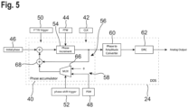
- Figure 5 shows a second variant of the first DDS module 24 described above or rather a second variant of the phase correction sub-module 58 of the first DDS module 24 described above.
- the phase correction sub-module 58 comprises a multiplexer sub-module 66 that is connected with the phase shift register 48 and with the phase shift trigger input 52.
- the phase correction sub-module 58 further comprises an adder sub-module 68 that is provided downstream of the multiplexer sub-module 66.
- the multiplexer sub-module 58 is configured to selectively forward a phase correction signal stored in the phase shift register 48 or a zero-signal to the adder sub-module 66, wherein the zero-signal does not alter the phase signal when added to the phase signal.
- the PSW saved in the phase shift register 48 corresponds to the phase correction signal, i.e. a difference between the desired phase signal and the actual phase signal output by the phase accumulator module 40 in the current clock cycle.
- the multiplexer sub-module 66 is controlled by the control- and trigger module 39 to forward the zero-signal to the adder sub-module 68 or to forward no signal at all.
- the multiplexer sub-module 66 is controlled to forward the phase correction signal to the adder sub-module 68 for exactly one clock cycle.
- phase correction signal is added to the phase signal fed back to the phase increment sub-module 54 by means of the adder sub-module 68, such that the phase signal fed back to the phase increment sub-module 54 is adapted for one clock cycle.
- phase correction signal may have positive or negative sign, i.e. the adder sub-module 68 may in fact add or subtract a certain phase value to or from the phase signal fed back to the phase increment sub-module 54.
- the measurement system 10 described above is configured to perform a method of operating the first DDS module 24. The method is described in the following with reference to Figure 6 .
- An analog output signal is generated by means of the first DDS module 24 and by means of the second DDS module 26, respectively (step S1).
- the control- and trigger module 39 may initialize the DDS modules 24, 26 by providing initial phase values to the initial phase registers 46 of the DDS modules 24, 26, and by providing FTWs to the frequency tuning registers 44 of the DDS modules 24, 26.
- the initial phase values are written into the initial phase registers 46, and the FTWs are written into the frequency tuning registers 44 of the DDS modules 24, 26.
- the control- and trigger module 39 may then control the DDS modules 24, 26 to start generating the analog outputs signals by generating an FTW trigger signal and by providing the FTW trigger signal to the FTW trigger inputs 50 of the DDS modules 24, 26. Upon receiving the FTW trigger signal, the DDS modules 24, 26 start generating the analog output signals.
- the analog output signals are forwarded to the analysis module 30 by means of the first directional coupler 36 and by means of the second directional coupler 38 (step S2).
- the phase determination unit 32 may determine the phase difference between the output signals with respect to certain measurement planes of the measurement system 10 based on calibration data, wherein the calibration data takes phase differences between the phase determination unit 32 and the measurement planes into account.
- the determined phase difference may correspond to the phase difference between the output signal of the first DDS module 24 at a first measurement plane and the output signal of the second DDS module at a second measurement plane.
- the measurement planes may be adaptable by a user, e.g. via the control means 20 of the measurement instrument 12.
- the determined phase difference is forwarded to the phase adjustment processing unit 34.
- a PSW is determined for the first DDS module 24 by means of the phase adjustment processing unit 34 based on the determined phase difference (step S4).
- control- and trigger module 39 may comprise a memory with a data set, wherein the data set comprises FTWs being compatible with the first DDS module 24 and corresponding PSWs.
- the PSW may be determined based on the data set, namely based on the FTW of the first DDS module 24, particularly based on the FTW provided to the frequency tuning registers 44 of the first DDS module 24 by means of the control- and trigger module 39.
- the PSW is forwarded to the phase shift register 48 of the first DDS module 24, and the PSW is written into the phase shift register 48 (step S5).
- the PSW may be forwarded to the phase shift register 48 of the first DDS module 24 directly or via the control- and trigger module 39.
- the phase of the output signal of the first DDS module 24 (at the respective measurement plane) is adapted by means of the phase correction sub-module 58 of the first DDS module 24 (step S6).
- a desired phase relation between the output signals of the DDS modules 24, 26 is obtained by adapting the phase of the output signal of the first DDS module 24.
- Steps S3 to S6 may be repeated in predefined time intervals.
- the phase relation between the analog output signals of the DDS modules 24, 26 may be monitored continuously, and the phase of the analog output signal of the first DDS module 24 may be corrected by providing an appropriate PSW to the first DDS module 24 if necessary.
- steps S1 to S6 described above may be performed after the FTW of at least one of the DDS modules 24, 26 has been updated.
- steps S1 to S6 described above may be performed after the FTW of at least one of the DDS modules 24, 26 has been updated.
- circuitry e.g., one or more circuits
- circuitry operably couple two or more components, generate information, process information, analyze information, generate signals, encode/decode signals, convert signals, transmit and/or receive signals, control other devices, etc.
- Circuitry of any type can be used.
- circuitry includes, among other things, one or more computing devices such as a processor (e.g., a microprocessor), a central processing unit (CPU), a digital signal processor (DSP), an application-specific integrated circuit (ASIC), a field-programmable gate array (FPGA), a system on a chip (SoC), or the like, or any combinations thereof, and can include discrete digital or analog circuit elements or electronics, or combinations thereof.
- a processor e.g., a microprocessor
- CPU central processing unit
- DSP digital signal processor
- ASIC application-specific integrated circuit
- FPGA field-programmable gate array
- SoC system on a chip
- circuitry includes hardware circuit implementations (e.g., implementations in analog circuitry, implementations in digital circuitry, and the like, and combinations thereof).
- circuitry includes combinations of circuits and computer program products having software or firmware instructions stored on one or more computer readable memories that work together to cause a device to perform one or more protocols, methodologies or technologies described herein.
- circuitry includes circuits, such as, for example, microprocessors or portions of microprocessor, that require software, firmware, and the like for operation.
- circuitry includes one or more processors or portions thereof and accompanying software, firmware, hardware, and the like.
- the present application may reference quantities and numbers. Unless specifically stated, such quantities and numbers are not to be considered restrictive, but exemplary of the possible quantities or numbers associated with the present application. Also in this regard, the present application may use the term “plurality” to reference a quantity or number. In this regard, the term “plurality” is meant to be any number that is more than one, for example, two, three, four, five, etc. The terms “about”, “approximately”, “near” etc., mean plus or minus 5% of the stated value.
Landscapes
- Engineering & Computer Science (AREA)
- Theoretical Computer Science (AREA)
- Physics & Mathematics (AREA)
- General Engineering & Computer Science (AREA)
- General Physics & Mathematics (AREA)
- Manipulation Of Pulses (AREA)
- Tests Of Electronic Circuits (AREA)
Abstract
A direct digital synthesizer (DDS) module (24) is described. The DDS module (24) comprises a phase accumulator module. The phase accumulator module comprises a clock input being configured to receive a clock signal. The phase accumulator module further comprises a frequency tuning register being configured to receive a frequency tuning word (FTW). The phase accumulator module further comprises a phase shift register being configured to receive a phase shift word (PSW). The phase accumulator module further comprises a phase increment sub-module being configured to increment a phase signal output by the phase accumulator module by a predetermined phase increment based on the clock signal and/or based on the FTW. The phase accumulator module further comprises a feedback path being configured to feed back the phase signal to the phase increment sub-module. The phase accumulator module further comprises a phase correction sub-module, wherein the phase correction sub-module is configured to adapt the phase signal fed back to the phase increment sub-module based on the phase shift word. Further, a measurement system (10) and a method of operating a direct digital synthesizer module (24) are described.
Description
- The invention generally relates to a direct digital synthesizer module. The invention further relates to a measurement system and to a method of operating a direct digital synthesizer module.
- Direct digital synthesizers are, referred to the CLK of the phase accumulator, highly phase stable. Modern direct digital synthesizers enable the user to set the frequency and initial phase via dedicated registers, namely via an FTW (frequency tuning word) and an initial phase.
- Certain measurement setups require two or more direct digital synthesizers having a predefined phase relation to each other. In the state of the art, this phase relation is usually achieved by setting the respective initial phase values of the direct digital synthesizers, wherein the initial phase values of all direct digital synthesizers have to be set simultaneously within a single clock cycle.
- Thus, setting the initial phase values of the direct digital synthesizers has to be timed in a very precise manner in order to set a desire phase relation between the direct digital synthesizers.
- The object of the present invention is to provide a direct signal synthesizer module that allows for a less time-critical setting of the phase relation.
- According to the present invention, the problem is solved by a direct digital synthesizer (DDS) module. The DDS module comprises a phase accumulator module. The phase accumulator module comprises a clock input being configured to receive a clock signal. The phase accumulator module further comprises a frequency tuning register being configured to receive a frequency tuning word (FTW). The phase accumulator module further comprises a phase shift register being configured to receive a phase shift word (PSW). The phase accumulator module further comprises a phase increment sub-module being configured to increment a phase signal output by the phase accumulator module by a predetermined phase increment based on the clock signal and/or based on the FTW. The phase accumulator module further comprises a feedback path being configured to feed back the phase signal to the phase increment sub-module. The phase accumulator module further comprises a phase correction sub-module, wherein the phase correction sub-module is configured to adapt the phase signal fed back to the phase increment sub-module based on the phase shift word.
- Therein and in the following, the term "module" is understood to describe suitable hardware, suitable software, or a combination of hardware and software that is configured to have a certain functionality.
- The hardware may, inter alia, comprise a CPU, a GPU, an FPGA, an ASIC, or other types of electronic circuitry.
- According to the present invention, the phase signal fed back to the phase increment sub-module is adapted based on the PSW in order to obtain a desired phase signal that is output by the phase accumulator module.
- In other words, the phase of an output signal of the DDS module is adapted by adapting the phase signal fed back to the phase increment sub-module based on the PSW.
- Thus, a desired phase relation between an output signal of the DDS module and another signal, e.g. another output signal of another DDS module, can be obtained by providing the PSW to the DDS module.
- In fact, the phase signal fed back to the phase increment sub-module can be adapted in an arbitrary clock cycle of the phase accumulator module.
- Thus, instead of initializing multiple DDS modules simultaneously, a phase correction is applied to the phase signal fed back to the phase increment sub-module, which is not time-critical and does not require a precise coordination of multiple different DDS modules.
- The DDS module may comprise a converter module downstream of the phase accumulator module, wherein the converter module is configured to convert the phase signal output by the phase accumulator module into an amplitude signal. In general, the converter module is configured to map the phase of the phase signal to a corresponding amplitude of the amplitude signal, such that signals having arbitrary shape can be generated, e.g. sine-shaped amplitude signals, sawtooth-shaped amplitude signals, etc.
- The DDS module may comprises a digital-to-analog converter (DAC) downstream of the phase accumulator module, particularly downstream of the converter module. The DAC is configured to convert a digital output signal of the DDS module, particularly the amplitude signal, into an analog output signal of the DDS module.
- The DDS module may be integrated on a chip. For example, the chip may be a dedicated DDS chip. However, it is to be understood that the DDS module may also be integrated on a chip together with other electronic components.
- According to an aspect of the present invention, the phase correction sub-module is configured to receive a phase shift trigger signal, wherein the phase correction sub-module is configured to adapt the phase signal fed back to the phase increment sub-module upon receiving the phase shift trigger signal. In other words, the timing of adapting the phase signal fed back to the phase increment sub-module can be controlled by providing the phase shift trigger signal to the phase correction sub-module.
- In an embodiment of the present invention, the phase correction sub-module is configured to replace the phase signal fed back to the phase increment sub-module with a corrected phase signal. Particularly, the phase correction sub-module comprises a multiplexer sub-module, wherein the multiplexer sub-module is configured to selectively forward the phase signal or the corrected phase signal to the phase increment sub-module. In other words, instead of feeding back an actual phase signal output by the phase increment sub-module, the corrected phase signal is fed back or rather forwarded to the phase increment sub-module. This way, an arbitrary phase signal can be set.
- Therein, the corrected phase signal may correspond to the desired phase signal that should be output by the phase accumulator module in the current clock cycle.
- During normal operation, the multiplexer sub-module may be configured or rather controlled to feed back the phase signal output by the phase increment sub-module to the phase increment sub-module.
- In order to adapt the phase of the (analog) output signal of the DDS module, the multiplexer sub-module is controlled to forward the corrected phase signal to the phase increment sub-module instead of the actual phase signal output by the phase increment sub-module for a predetermined time interval, e.g. for one clock cycle.
- For example, the multiplexer sub-module may be controlled by means of the phase shift trigger signal described above, such that the multiplexer sub-module forwards the corrected phase signal to the phase increment sub-module upon receiving the phase shift trigger signal.
- According to another aspect of the present invention, the phase correction sub-module is configured to replace the phase signal fed back to the phase increment sub-module with a corrected phase signal during a single clock cycle of the clock signal. Accordingly, during a certain clock cycle, the phase correction sub-module receives the corrected phase signal instead of the phase signal output by the phase correction sub-module. During the next clock cycle, the phase correction sub-module receives the phase signal output by the phase correction sub-module via the feedback path, which corresponds to the corrected phase signal incremented by the predetermined phase increment. Thus, the correction or rather adaptation of the phase of the output signal of the DDS module can be performed within a single clock cycle.
- A further aspect of the present invention provides that the phase correction sub-module is configured to add a phase correction signal to the phase signal fed back to the phase increment sub-module. Particularly, the phase correction sub-module comprises an adder sub-module, wherein the adder sub-module is configured to add the phase correction signal to the phase signal fed back to the phase increment sub-module. In other words, the phase signal output by the phase increment sub-module is corrected by adding the phase correction signal, such that a desired phase signal is obtained.
- Accordingly, the phase correction signal may correspond to the difference between the desired phase signal and the actual phase signal output by the phase accumulator module in the current clock cycle.
- The phase correction sub-module may comprise a multiplexer sub-module, wherein the multiplexer sub-module is configured to selectively forward the phase correction signal to the adder sub-module. More precisely, the multiplexer sub-module is configured to selectively forward the phase correction signal or a zero-signal to the adder sub-module, wherein the zero-signal does not alter the phase signal when added to the phase signal.
- During normal operation, the multiplexer sub-module may be configured or rather controlled to forward the zero-signal to the adder sub-module or to forward no signal at all.
- In order to adapt the phase of the (analog) output signal of the DDS module, the multiplexer sub-module is controlled to forward the phase correction signal to the adder sub-module for a predetermined time interval, e.g. for one clock cycle.
- For example, the multiplexer sub-module may be controlled by means of the phase shift trigger signal described above, such that the multiplexer sub-module forwards the phase correction signal to the adder sub-module upon receiving the phase shift trigger signal.
- Particularly, the phase correction sub-module is configured to add the phase correction signal to the phase signal fed back to the phase increment sub-module during a single clock cycle of the clock signal. Thus, the correction or rather adaptation of the phase of the output signal of the DDS module can be performed within a single clock cycle.
- According to the invention, the problem further is solved by a measurement system. The measurement system comprises at least one DDS module described above.
- Regarding the advantages and further properties of the measurement system, reference is made to the explanations given above with respect to the DDS module, which also hold for the measurement system and vice versa.
- The measurement system may comprise a measurement instrument, wherein the at least one DDS module is integrated into the measurement instrument. For example, the measurement instrument may be an oscilloscope, particularly a digital oscilloscope, a vector network analyzer, a spectrum analyzer, a standalone signal generator, etc.
- According to an aspect of the present invention, the measurement system comprises an analysis module, wherein the analysis module is configured to receive an analog output signal of the at least one DDS module, wherein the analysis module is further configured to receive a phase reference signal, and wherein the analysis module is configured to determine the PSW based on the analog output signal of the at least one DDS module and based on the phase reference signal.
- Particularly, the analysis module may be configured to determine a phase difference between the analog output signal of the at least one DDS module and the phase reference signal. The analysis module may further be configured to determine the PSW based on the determined phase difference.
- The analysis module may further be configured to forward the determined PSW to the at least one DDS module, or more precisely to the phase shift register of the at least one DDS module.
- The analysis module may be integrated into the measurement instrument described above.
- However, it is also conceivable that the analysis module is integrated into another electronic device.
- According to another aspect of the present invention, the measurement system comprises at least one further DDS module, wherein the phase reference signal is an analog output signal of the at least one further DDS module.
- The at least one further DDS module may be configured like the DDS module described above, but this is not necessary.
- In fact, in order to set a particular phase relation of analog outputs signals of two DDS modules, only a single PSW has to be determined for one of the two DDS modules.
- If a total number of N DDS modules is provided, and phase relations between the N DDS modules are to be set, (N-1) PSWs have to be determined by means of the analysis module.
- In fact, the phases of the analog output signals of (N-1) DDS modules may be adapted relative to the phase of the analog output signal of the remaining DDS module based on the (N-1) determined PSWs.
- Particularly, the analysis module is configured to repeatedly determine the PSW in predefined time intervals. In other words, the phase relation between the analog output signal of the at least one DDS module and the phase reference signal may be monitored continuously, and the phase of the analog output signal of the at least one DDS module may be corrected by providing an appropriate PSW to the at least one DDS module if necessary.
- Alternatively or additionally, the analysis module may be configured to determine the PSW after the FTW of the at least one DDS module has been updated. Thus, it is ensured that a desired phase relation between the analog output signal of the at least one DDS module and the phase reference signal is obtained after the FTW has been updated.
- In an embodiment of the present invention, the measurement system comprises a directional coupler, wherein the directional coupler is configured to forward the analog output signal of the at least one DDS module to the analysis module. The directional coupler may further be configured to forward the analog output signal of the at least one DDS module to a measurement port, to another electronic component, or to another signal path.
- Particularly, the directional coupler is established as a 3-port coupler.
- The measurement system may comprise at least one further directional coupler, wherein the at least one further directional coupler is configured to forward the phase reference signal the analysis module. The at least one further directional coupler may further be configured to forward the phase reference signal to a measurement port, to another electronic component, or to another signal path.
- Particularly, the at least one further directional coupler is established as a 3-port coupler.
- The measurement system may comprise at least one further DDS module, wherein the measurement system comprises a common clock source for the at least one DDS module and for the at least one further DDS module.
- However, it is also conceivable that different clock sources are provided for the at least one DDS module and for the at least one further DDS module.
- According to the invention, the problem further is solved by a method of operating a direct digital synthesizer (DDS) module, wherein the DDS module is established as described above. The method comprises the steps of:
- generating, by means of the DDS module, an analog output signal;
- receiving, by means of an analysis module, the analog output signal and a phase reference signal;
- determining, by means of the analysis module, a PSW based on the analog output signal and based on the phase reference signal; and
- adapting, by means of the phase correction sub-module of the DDS module, the phase signal output by the phase accumulator module based on the PSW.
- Regarding the further advantages and properties of the method, reference is made to the explanations given above with respect to the DDS module and the measurement system, which also hold for the method and vice versa.
- The foregoing aspects and many of the attendant advantages of the claimed subject matter will become more readily appreciated as the same become better understood by reference to the following detailed description, when taken in conjunction with the accompanying drawings, wherein:
-
Figure 1 schematically shows a measurement system according to the present invention; -
Figure 2 schematically shows a signal generator module of the measurement system ofFigure 1 in more detail; -
Figure 3 schematically shows a DDS module according to the present invention; -
Figure 4 schematically shows a first variant of the DDS module ofFigure 3 -
Figure 5 schematically shows a second variant of the DDS module ofFigure 3 ; and -
Figure 6 shows a flow chart of a method of operating a DDS module according to the present invention. - The detailed description set forth below in connection with the appended drawings, where like numerals reference like elements, is intended as a description of various embodiments of the disclosed subject matter and is not intended to represent the only embodiments. Each embodiment described in this disclosure is provided merely as an example or illustration and should not be construed as preferred or advantageous over other embodiments. The illustrative examples provided herein are not intended to be exhaustive or to limit the claimed subject matter to the precise forms disclosed.
- For the purposes of the present disclosure, the phrase "at least one of A, B, and C", for example, means (A), (B), (C), (A and B), (A and C), (B and C), or (A, B, and C), including all further possible permutations when more than three elements are listed. In other words, the term "at least one of A and B" generally means "A and/or B", namely "A" alone, "B" alone or "A and B".
-
Figure 1 schematically shows ameasurement system 10 comprising ameasurement instrument 12 and a device undertest 14. - In general, the
measurement instrument 12 may be established as any type of measurement instrument being suitable to perform measurements on the electronic device undertest 14. - For example, the
measurement instrument 12 may be established as an oscilloscope, particularly as a digital oscilloscope, as a vector network analyzer, as a spectrum analyzer, as a signal generator, etc. - The
measurement instrument 12 comprises twomeasurement ports 16, wherein measurements can be conducted on the device undertest 14 via themeasurement ports 16. - In general, signals can be received from the device under
test 14 and/or forwarded to the device undertest 14 via themeasurement ports 16 in order to perform the measurements on the device undertest 14. - It is to be understood that the
measurement instrument 12 may comprise an arbitrary number ofmeasurement ports 16 other than two. - The
measurement instrument 12 may further comprise adisplay 18 and/or control means 20, wherein settings of themeasurement instrument 12 may be adaptable by a user via the control means 20. - The
measurement instrument 12 further comprises asignal generator module 22 that is shown in more detail inFigure 2 . - In the exemplary embodiment shown in
Figure 2 , thesignal generator module 22 comprises a first direct digital synthesizer (DDS)module 24 and asecond DDS module 26. - The
first DDS module 24 and thesecond DDS module 26 are configured to generate an analog output signal, respectively. - Accordingly, the
signal generator module 22 is configured to generate two analog outputs signals that may be employed in order to conduct measurements on the device undertest 14. - However, it is to be understood that the
measurement system 10, particularly thesignal generator module 22, may comprise an arbitrary number of DDS modules. - For example, the analog output signals may be used as reference signals for conducting the measurements.
- As another example, the analog output signals may be forwarded to different ports of the device under
test 14, particularly wherein the analog output signals may correspond to a differential signal. The analog output signals may be processed by the device undertest 14 and/or partially reflected at input ports of the device undertest 14, and the corresponding processed and/or reflected signals may be measured by means of themeasurement instrument 12. - In the exemplary embodiment shown in
Figure 2 , thesignal generator module 22 further comprises aclock source 28 that is configured to provide a clock signal to thefirst DDS module 24 and to thesecond DDS module 26. - However, it is also conceivable that the
signal generator module 22 comprises a dedicated clock source for eachDDS module - The
signal generator module 22 further comprises ananalysis module 30 that comprises aphase determination unit 32 and a phaseadjustment processing unit 34, the functionality of which will be described in more detail below. - The
signal generator module 22 further comprises a firstdirectional coupler 36 that is configured to forward the analog output signal of thefirst DDS module 24 to theanalysis module 30. The firstdirectional coupler 36 is further configured to forward the analog output signal of thefirst DDS module 24 to one of themeasurement ports 16 or to another electronic component of themeasurement instrument 12. - In fact, the first
directional coupler 36 is established as a 3-port coupler. - The
signal generator module 22 further comprises a seconddirectional coupler 38 that is configured to forward the analog output signal of thesecond DDS module 26 to theanalysis module 30. The seconddirectional coupler 38 is further configured to forward the analog output signal of thesecond DDS module 26 to one of themeasurement ports 16 or to another electronic component of themeasurement instrument 12. - The second
directional coupler 38 is established as a 3-port coupler. - The
signal generator module 22 further comprises a control- and trigger module 39, the functionality of which will be described in more detail below. -
Figure 3 schematically shows a first variant of thefirst DDS module 24. - For example, the
first DDS module 24 may be integrated on a dedicated DDS chip. Alternatively, thefirst DDS module 24 may be integrated on a chip together with other electronic components of themeasurement instrument 12. - The
DDS module 24 comprises aphase accumulator module 40. - The
phase accumulator module 40 comprises aclock input 42 that is configured to receive a clock signal having a predefined frequency, namely the clock signal generated by theclock source 28. - The
phase accumulator module 40 further comprises afrequency tuning register 44 that is configured to receive and save a frequency tuning word (FTW), particularly from the control- and trigger module 39. - In general, the FTW determines a frequency of an output signal of the
DDS module 24 in relation to the frequency of the clock signal, as is well-known in the state of the art related to direct digital synthesizers. - The
phase accumulator module 40 further comprises an initial phase register 46 being configured to receive and save an initial phase for thephase accumulator module 40. - It is noted that the
frequency tuning register 44 and theinitial phase register 46 may also be integrated into a single register. - The
phase accumulator module 40 further comprises aphase shift register 48 being configured to receive and save a phase shift word (PSW), particularly from the control- and trigger module 39 and/or from theanalysis module 30. - Moreover, the
phase accumulator module 40 comprises anFTW trigger input 50 and a phaseshift trigger input 52. - The FTW trigger
input 50 is configured to receive an FTW trigger signal, particularly from the control- and trigger module 39. - The phase
shift trigger input 52 is configured to receive a phase shift trigger signal, particularly from the control- and trigger module 39. - The
phase accumulator module 40 further comprises aphase increment sub-module 54 and afeedback path 56. - The
phase increment sub-module 54 is configured to increment a phase signal output by thephase accumulator module 40 by a predetermined phase increment based on the clock signal and/or based on the FTW. - The
feedback path 56 is configured to feed back the phase signal to thephase increment sub-module 54. - The
phase accumulator module 40 further comprises aphase correction sub-module 58. In general, thephase correction sub-module 58 is configured to adapt the phase signal fed back to thephase increment sub-module 54 based on the PSW, as will be described in more detail below. - In the embodiment shown in
Figure 3 , thefirst DDS module 24 further comprises aconverter module 60 and a digital-to-analog converter (DAC) 62. - The
converter module 60 is provided downstream of thephase accumulator module 40, and is configured to convert the phase signal output by thephase accumulator module 40 into an amplitude signal. - In general, the
converter module 60 is configured to map the phase of the phase signal to a corresponding amplitude of the amplitude signal, such that signals having arbitrary shape can be generated, e.g. sine-shaped amplitude signals, sawtooth-shaped amplitude signals, etc. - The
DAC 62 is provided downstream of theconverter module 60. TheDAC 62 is configured to convert a digital output signal of thefirst DDS module 24, namely the amplitude signal output by theconverter module 60, into an analog output signal of thefirst DDS module 24. - The
second DDS module 26 may be established identically to thefirst DDS module 24 described above and hereinafter. - However, in principle the
second DDS module 26 may be established without thephase shift register 48, the phaseshift trigger input 52, and thephase correction sub-module 58. -
Figure 4 shows a first variant of thefirst DDS module 24 described above or rather of thephase correction sub-module 58 of thefirst DDS module 24 described above. - The
phase correction sub-module 58 comprises amultiplexer sub-module 64 that is connected with thephase increment sub-module 54 via thefeedback path 56. - Moreover, the
multiplexer sub-module 64 is connected with thephase shift register 48 and with the phaseshift trigger input 52. - The
multiplexer sub-module 64 is configured to selectively forward the phase signal output by thephase increment sub-module 54 or a corrected phase signal to thephase increment sub-module 54. - Thus, in this case, the PSW saved in the
phase shift register 48 corresponds to the corrected phase signal, i.e. a desired phase signal that should be output by thephase accumulator module 40 in the current clock cycle. - During normal operation, the
multiplexer sub-module 64 is controlled by the control- and trigger module 39 to feed back the phase signal output by thephase increment sub-module 54 to thephase increment sub-module 54. - In order to adapt the phase of the (analog) output signal of the
first DDS module 24, themultiplexer sub-module 64 is controlled by the control- and trigger module 39 to forward the corrected phase signal saved in thephase shift register 48 to the phase increment sub-module 54 for exactly one clock cycle of the clock signal. - In other words, the phase signal output by the
phase increment sub-module 54 is replaced by the corrected phase signal for one clock cycle. - In fact, the control- and trigger module 39 generates a phase shift trigger signal that is forwarded to the
multiplexer sub-module 64 via the phaseshift trigger input 52. Upon receiving the phase shift trigger signal, themultiplexer sub-module 64 forwards the corrected phase signal saved in thephase shift register 48 to the phase increment sub-module 54 for exactly one clock cycle. -
Figure 5 shows a second variant of thefirst DDS module 24 described above or rather a second variant of thephase correction sub-module 58 of thefirst DDS module 24 described above. - The
phase correction sub-module 58 comprises amultiplexer sub-module 66 that is connected with thephase shift register 48 and with the phaseshift trigger input 52. - The
phase correction sub-module 58 further comprises anadder sub-module 68 that is provided downstream of themultiplexer sub-module 66. - The
multiplexer sub-module 58 is configured to selectively forward a phase correction signal stored in thephase shift register 48 or a zero-signal to theadder sub-module 66, wherein the zero-signal does not alter the phase signal when added to the phase signal. - Thus, in this case, the PSW saved in the
phase shift register 48 corresponds to the phase correction signal, i.e. a difference between the desired phase signal and the actual phase signal output by thephase accumulator module 40 in the current clock cycle. - During normal operation, the
multiplexer sub-module 66 is controlled by the control- and trigger module 39 to forward the zero-signal to theadder sub-module 68 or to forward no signal at all. - In order to adapt the phase of the (analog) output signal of the
first DDS module 24, themultiplexer sub-module 66 is controlled to forward the phase correction signal to the adder sub-module 68 for exactly one clock cycle. - The phase correction signal is added to the phase signal fed back to the
phase increment sub-module 54 by means of theadder sub-module 68, such that the phase signal fed back to thephase increment sub-module 54 is adapted for one clock cycle. - Therein, it is to be understood that the phase correction signal may have positive or negative sign, i.e. the
adder sub-module 68 may in fact add or subtract a certain phase value to or from the phase signal fed back to thephase increment sub-module 54. - The
measurement system 10 described above is configured to perform a method of operating thefirst DDS module 24. The method is described in the following with reference toFigure 6 . - An analog output signal is generated by means of the
first DDS module 24 and by means of thesecond DDS module 26, respectively (step S1). - The control- and trigger module 39 may initialize the
DDS modules DDS modules DDS modules - The initial phase values are written into the initial phase registers 46, and the FTWs are written into the frequency tuning registers 44 of the
DDS modules - The control- and trigger module 39 may then control the
DDS modules FTW trigger inputs 50 of theDDS modules DDS modules - The analog output signals are forwarded to the
analysis module 30 by means of the firstdirectional coupler 36 and by means of the second directional coupler 38 (step S2). - A phase difference between the output signals of the
DDS modules - Therein, the
phase determination unit 32 may determine the phase difference between the output signals with respect to certain measurement planes of themeasurement system 10 based on calibration data, wherein the calibration data takes phase differences between thephase determination unit 32 and the measurement planes into account. - Accordingly, the determined phase difference may correspond to the phase difference between the output signal of the
first DDS module 24 at a first measurement plane and the output signal of the second DDS module at a second measurement plane. - For example, the measurement planes may be adaptable by a user, e.g. via the control means 20 of the
measurement instrument 12. - The determined phase difference is forwarded to the phase
adjustment processing unit 34. - A PSW is determined for the
first DDS module 24 by means of the phaseadjustment processing unit 34 based on the determined phase difference (step S4). - Alternatively or additionally to steps S3 and S4 described above, the control- and trigger module 39 may comprise a memory with a data set, wherein the data set comprises FTWs being compatible with the
first DDS module 24 and corresponding PSWs. - Accordingly, the PSW may be determined based on the data set, namely based on the FTW of the
first DDS module 24, particularly based on the FTW provided to the frequency tuning registers 44 of thefirst DDS module 24 by means of the control- and trigger module 39. - The PSW is forwarded to the
phase shift register 48 of thefirst DDS module 24, and the PSW is written into the phase shift register 48 (step S5). - The PSW may be forwarded to the
phase shift register 48 of thefirst DDS module 24 directly or via the control- and trigger module 39. - The phase of the output signal of the first DDS module 24 (at the respective measurement plane) is adapted by means of the
phase correction sub-module 58 of the first DDS module 24 (step S6). - Accordingly, a desired phase relation between the output signals of the
DDS modules first DDS module 24. - More precisely, as described above, the control- and trigger module 39 generates a phase shift trigger signal that causes the
phase correction sub-module 58 to adapt the phase of the phase signal fed back to the phase-increment sub-module 54 during a single clock cycle. Thereby, the phase of the output signal of thefirst DDS module 24 is adapted, particularly in the next clock cycle. - Steps S3 to S6 may be repeated in predefined time intervals. Thus, the phase relation between the analog output signals of the
DDS modules first DDS module 24 may be corrected by providing an appropriate PSW to thefirst DDS module 24 if necessary. - Alternatively or additionally, steps S1 to S6 described above may be performed after the FTW of at least one of the
DDS modules DDS modules - Certain embodiments disclosed herein, particularly the respective module(s) and/or unit(s), utilize circuitry (e.g., one or more circuits) in order to implement standards, protocols, methodologies or technologies disclosed herein, operably couple two or more components, generate information, process information, analyze information, generate signals, encode/decode signals, convert signals, transmit and/or receive signals, control other devices, etc. Circuitry of any type can be used.
- In an embodiment, circuitry includes, among other things, one or more computing devices such as a processor (e.g., a microprocessor), a central processing unit (CPU), a digital signal processor (DSP), an application-specific integrated circuit (ASIC), a field-programmable gate array (FPGA), a system on a chip (SoC), or the like, or any combinations thereof, and can include discrete digital or analog circuit elements or electronics, or combinations thereof. In an embodiment, circuitry includes hardware circuit implementations (e.g., implementations in analog circuitry, implementations in digital circuitry, and the like, and combinations thereof).
- In an embodiment, circuitry includes combinations of circuits and computer program products having software or firmware instructions stored on one or more computer readable memories that work together to cause a device to perform one or more protocols, methodologies or technologies described herein. In an embodiment, circuitry includes circuits, such as, for example, microprocessors or portions of microprocessor, that require software, firmware, and the like for operation. In an embodiment, circuitry includes one or more processors or portions thereof and accompanying software, firmware, hardware, and the like.
- The present application may reference quantities and numbers. Unless specifically stated, such quantities and numbers are not to be considered restrictive, but exemplary of the possible quantities or numbers associated with the present application. Also in this regard, the present application may use the term "plurality" to reference a quantity or number. In this regard, the term "plurality" is meant to be any number that is more than one, for example, two, three, four, five, etc. The terms "about", "approximately", "near" etc., mean plus or minus 5% of the stated value.
Claims (15)
- A direct digital synthesizer (DDS) module, the DDS module (24) comprising a phase accumulator module (40),wherein the phase accumulator module (40) comprises a clock input (42) being configured to receive a clock signal,wherein the phase accumulator module (40) further comprises a frequency tuning register (44) being configured to receive a frequency tuning word (FTW),wherein the phase accumulator module (40) further comprises a phase shift register (48) being configured to receive a phase shift word (PSW),wherein the phase accumulator module (40) further comprises a phase increment sub-module (54) being configured to increment a phase signal output by the phase accumulator module (40) by a predetermined phase increment based on the clock signal and/or based on the FTW,wherein the phase accumulator module (40) further comprises a feedback path (56) being configured to feed back the phase signal to the phase increment sub-module (54), andwherein the phase accumulator module (40) further comprises a phase correction sub-module (58), wherein the phase correction sub-module (58) is configured to adapt the phase signal fed back to the phase increment sub-module (54) based on the phase shift word.
- The DDS module of claim 1, wherein the phase correction sub-module (58) is configured to receive a phase shift trigger signal, and wherein the phase correction sub-module (58) is configured to adapt the phase signal fed back to the phase increment sub-module (54) upon receiving the phase shift trigger signal.
- The DDS module according to any one of the preceding claims, wherein the phase correction sub-module (58) is configured to replace the phase signal fed back to the phase increment sub-module (54) with a corrected phase signal, particularly wherein the phase correction sub-module (58) comprises a multiplexer sub-module (64), wherein the multiplexer sub-module (64) is configured to selectively forward the phase signal or the corrected phase signal to the phase increment sub-module.
- The DDS module of claim 3, wherein the phase correction sub-module (58) is configured to replace the phase signal fed back to the phase increment sub-module (54) with a corrected phase signal during a single clock cycle of the clock signal.
- The DDS module according to any one of the preceding claims, wherein the phase correction sub-module (58) is configured to add a phase correction signal to the phase signal fed back to the phase increment sub-module (54), particularly wherein the phase correction sub-module (58) comprises an adder sub-module (68), wherein the adder sub-module (68) is configured to add the phase correction signal to the phase signal fed back to the phase increment sub-module (54).
- The DDS module of claim 5, wherein the phase correction sub-module (58) comprises a multiplexer sub-module (66), wherein the multiplexer sub-module (68) is configured to selectively forward the phase correction signal to the adder sub-module (68).
- The DDS module of claim 5 or 6, wherein the phase correction sub-module (58) is configured to add the phase correction signal to the phase signal fed back to the phase increment sub-module (54) during a single clock cycle of the clock signal.
- A measurement system, comprising at least one DDS module (24) according to any one of claims 1 to 7.
- The measurement system of claim 8, comprising a measurement instrument (12), wherein the at least one DDS module (24) is integrated into the measurement instrument (12).
- The measurement system of claim 8 or 9, further comprising an analysis module (30), wherein the analysis module (30) is configured to receive an analog output signal of the at least one DDS module (24), wherein the analysis module (30) is further configured to receive a phase reference signal, and wherein the analysis module (30) is configured to determine the PSW based on the analog output signal of the at least one DDS module (24) and based on the phase reference signal.
- The measurement system of claim 10, wherein the measurement system (10) comprises at least one further DDS module (26), and wherein the phase reference signal is an analog output signal of the at least one further DDS module (26).
- The measurement system according to any one of claims 10 to 11, wherein the analysis module (30) is configured to repeatedly determine the PSW in predefined time intervals.
- The measurement system according to any one of claims 8 to 12, wherein the measurement system (10) comprises a directional coupler (36), and wherein the directional coupler (36) is configured to forward the analog output signal of the at least one DDS module (24) to the analysis module (30).
- The measurement system according to any one of claims 8 to 13, wherein the measurement system (10) comprises at least one further DDS module (26), and wherein the measurement system (10) comprises a common clock source (28) for the at least one DDS module (24) and for the at least one further DDS module (26).
- A method of operating a direct digital synthesizer (DDS) module (24), wherein the DDS module (24) is established according to any one of claims 1 to 7, the method comprising the steps of:- generating, by means of the DDS module (24), an analog output signal;- receiving, by means of an analysis module (30), the analog output signal and a phase reference signal;- determining, by means of the analysis module (30), a PSW based on the analog output signal and based on the phase reference signal; and- adapting, by means of the phase correction sub-module (58) of the DDS module (24), the phase signal output by the phase accumulator module (40) based on the PSW.
Priority Applications (2)
| Application Number | Priority Date | Filing Date | Title |
|---|---|---|---|
| EP22216129.1A EP4391385A1 (en) | 2022-12-22 | 2022-12-22 | Direct digital synthesizer module, measurement system, and method of operating a direct digital synthesizer module |
| US18/543,676 US12608036B2 (en) | 2022-12-22 | 2023-12-18 | Direct digital synthesizer circuit, measurement system, and method of operating a direct digital synthesizer circuit |
Applications Claiming Priority (1)
| Application Number | Priority Date | Filing Date | Title |
|---|---|---|---|
| EP22216129.1A EP4391385A1 (en) | 2022-12-22 | 2022-12-22 | Direct digital synthesizer module, measurement system, and method of operating a direct digital synthesizer module |
Publications (1)
| Publication Number | Publication Date |
|---|---|
| EP4391385A1 true EP4391385A1 (en) | 2024-06-26 |
Family
ID=84799715
Family Applications (1)
| Application Number | Title | Priority Date | Filing Date |
|---|---|---|---|
| EP22216129.1A Pending EP4391385A1 (en) | 2022-12-22 | 2022-12-22 | Direct digital synthesizer module, measurement system, and method of operating a direct digital synthesizer module |
Country Status (2)
| Country | Link |
|---|---|
| US (1) | US12608036B2 (en) |
| EP (1) | EP4391385A1 (en) |
Citations (3)
| Publication number | Priority date | Publication date | Assignee | Title |
|---|---|---|---|---|
| GB2352346A (en) * | 1999-07-22 | 2001-01-24 | Wavetek Ltd | Direct digital synthesis of variable frequency waveforms |
| US9244885B1 (en) * | 2013-03-15 | 2016-01-26 | Xilinx, Inc. | Pipelined phase accumulator |
| US20160164531A1 (en) * | 2013-11-28 | 2016-06-09 | Smart Energy Instrumetns Inc. | Methods and devices for error correction of a signal using delta sigma modulation |
Family Cites Families (7)
| Publication number | Priority date | Publication date | Assignee | Title |
|---|---|---|---|---|
| JP2861542B2 (en) | 1991-10-25 | 1999-02-24 | 日本電気株式会社 | Phase locked loop synthesizer |
| US6236267B1 (en) * | 1998-12-29 | 2001-05-22 | International Business Machines Corporation | Linearization for power amplifiers using feed-forward and feedback control |
| JP2008079261A (en) * | 2006-09-25 | 2008-04-03 | Yokogawa Electric Corp | Standard signal generator and standard signal generation system |
| US7714623B2 (en) | 2008-04-09 | 2010-05-11 | Ut-Battelle, Llc | Agile high resolution arbitrary waveform generator with jitterless frequency stepping |
| MY186548A (en) * | 2012-11-28 | 2021-07-26 | Agensi Remote Sensing Malaysia | Reconfigurable real-time synthetic aperture radar signal generator and method of providing the same |
| US9520831B1 (en) | 2014-06-26 | 2016-12-13 | Keysight Technologies, Inc. | Method and apparatus for synthesizing signals with phase continuous and phase coherent transitions |
| US10705556B2 (en) | 2017-09-29 | 2020-07-07 | International Business Machines Corporation | Phase continuous signal generation using direct digital synthesis |
-
2022
- 2022-12-22 EP EP22216129.1A patent/EP4391385A1/en active Pending
-
2023
- 2023-12-18 US US18/543,676 patent/US12608036B2/en active Active
Patent Citations (3)
| Publication number | Priority date | Publication date | Assignee | Title |
|---|---|---|---|---|
| GB2352346A (en) * | 1999-07-22 | 2001-01-24 | Wavetek Ltd | Direct digital synthesis of variable frequency waveforms |
| US9244885B1 (en) * | 2013-03-15 | 2016-01-26 | Xilinx, Inc. | Pipelined phase accumulator |
| US20160164531A1 (en) * | 2013-11-28 | 2016-06-09 | Smart Energy Instrumetns Inc. | Methods and devices for error correction of a signal using delta sigma modulation |
Non-Patent Citations (1)
| Title |
|---|
| BOZIC M ET AL: "Elimination of non-harmonic spurious in direct digital synthesis", 19930101, 1 January 1993 (1993-01-01), pages 6/1 - 6/8, XP006520835 * |
Also Published As
| Publication number | Publication date |
|---|---|
| US20240210985A1 (en) | 2024-06-27 |
| US12608036B2 (en) | 2026-04-21 |
Similar Documents
| Publication | Publication Date | Title |
|---|---|---|
| US9397670B2 (en) | Edge generator-based phase locked loop reference clock generator for automated test system | |
| EP0380979A2 (en) | Phased locked loop to provide precise frequency and phase tracking of two signals | |
| US5566188A (en) | Low cost timing generator for automatic test equipment operating at high data rates | |
| JP4565992B2 (en) | DDS circuit with arbitrary frequency control clock | |
| US5013944A (en) | Programmable delay line utilizing measured actual delays to provide a highly accurate delay | |
| KR20010006867A (en) | A-d converting apparatus, and calibration unit and method therefor | |
| CN110830034A (en) | Apparatus and method for radar chip synchronization | |
| JP2000293259A (en) | Delay clock generating device and delay time measuring instrument | |
| US6557133B1 (en) | Scaling logic for event based test system | |
| EP0322308A2 (en) | Delay line control system for automatic test equipment | |
| CN116744180A (en) | Signal processing method and signal processing system | |
| EP4478056A1 (en) | Signal processing method and measurement system | |
| CN114253346B (en) | Timing signal generator and calibration system and method thereof | |
| JP6651697B2 (en) | Electronic circuit, power supply circuit, method for measuring circuit characteristics, and program for calculating amplitude and phase characteristics | |
| US9292035B2 (en) | Packet based DDS minimizing mathematical and DAC noise | |
| US12608036B2 (en) | Direct digital synthesizer circuit, measurement system, and method of operating a direct digital synthesizer circuit | |
| US5964894A (en) | IC test equipment, measurement method in the IC test equipment, and storage medium of the same | |
| US6842055B1 (en) | Clock adjustment | |
| US11187736B2 (en) | Method of setting an analyzer for testing a device under test | |
| Patel et al. | Serialized control interface asic for distributed controllers of space-borne radar | |
| EP4575709B1 (en) | Synchronization method and measurement system | |
| EP4641242A1 (en) | Signal generator system and method for calibrating a signal generator system | |
| US12613275B2 (en) | Test and/or measurement system | |
| JP2002267725A (en) | Digital circuit device and semiconductor device testing method | |
| JPH026769A (en) | Timing signal generating circuit for tester |
Legal Events
| Date | Code | Title | Description |
|---|---|---|---|
| PUAI | Public reference made under article 153(3) epc to a published international application that has entered the european phase |
Free format text: ORIGINAL CODE: 0009012 |
|
| STAA | Information on the status of an ep patent application or granted ep patent |
Free format text: STATUS: REQUEST FOR EXAMINATION WAS MADE |
|
| 17P | Request for examination filed |
Effective date: 20231215 |
|
| AK | Designated contracting states |
Kind code of ref document: A1 Designated state(s): AL AT BE BG CH CY CZ DE DK EE ES FI FR GB GR HR HU IE IS IT LI LT LU LV MC ME MK MT NL NO PL PT RO RS SE SI SK SM TR |